LY2886721_1262036-50-9_DataSheet_MedChemExpress
IT-158BS TC 中等热转变温度(Tg)多功能填充环氧树脂和酚醛固化无铅层压板和预浸料说明书

IT-158BS/IT-158TCMultifunctional Filled Epoxy Resin and Phenolic-Cured Lead Free Laminate & PrepregIT-158 is a medium Tg (>150℃ by DSC) multifunctional filled epoxy with high thermal reliability and CAF resistance. It’s suitable for industrial PCB, automobile and can pass 260℃ Lead free assembly.Key Features =============================== Advanced Resin TechnologyIndustrial standard material with medium Tg (150℃ by DSC) multifunctional filled epoxy resin and excellent thermal reliability.Lead-Free Assembly CompatibleRoHS compliant and suitable for high thermal reliability needs, and Lead free assemblies with a maximum reflow temperature of 260℃. Friendly Processing and CAF ResistanceFriendly to PCB process that users can easily handle the process by current equipment and chemical.CAF ResistanceExcellent thermal reliability and CAF resistance providing long-term reliability for industrial boards and automobile application.Available in Variety of ConstructionsAvailable in a various of constructions, copper weights and glass styles, including standard(HTE), RTF and VLP copper foil. ApplicationsPC and Notebook Memory ModuleGame PlayerMultilayer PCB AutomobileServers and Networking Telecommunications Heavy Copper ApplicationIndustrial Approval UL 94 V-0IPC-4101C Spec / 99 RoHS CompliantREV 09-14ITEQ Laminate/ Prepreg : IT-158TC / IT-158BSIPC-4101C Spec /99LAMINATE (IT-158TC)Thickness<0.50 mm[0.0197 in] Thickness≧0.50 mm[0.0197 in] Units T est MethodPropertyTypical Value Spec Typical Value SpecMetric(English)IPC-TM-650(or as noted)Peel Strength, minimumA. Low profile copper foil and very low profile copperfoil - all copper weights > 17µm [0.669 mil]B. Standard profile copper foil1.After Thermal Stress2.At 125°C [257 F]3.After Process Solutions 0.88 (5.0)1.58 (9.0)1.31 (7.5)1.14 (6.5)0.70 (4.00)0.80 (4.57)0.70 (4.00)0.55 (3.14)0.88 (5.0)1.66 (9.5)1.40 (8.0)1.23 (7.0)0.70 (4.00)1.05 (6.00)0.70 (4.00)0.80 (4.57)N/mm(lb/inch)2.4.82.4.8.22.4.8.3Volume Resistivity, minimumA. C-96/35/90B. After moisture resistanceC. At elevated temperature E-24/125 3.0x10¹⁰--5.0x1010106--103--5.0x10101.0x1010--104103MΩ-cm 2.5.17.1Surface Resistivity, minimumA. C-96/35/90B. After moisture resistanceC. At elevated temperature E-24/125 1.0x10¹⁰--5.0x1010104--103--1.0x10103.0x1010--104103MΩ 2.5.17.1Moisture Absorption, maximum -- -- 0.08 0.5 % 2.6.2.1 Dielectric Breakdown, minimum -- -- 60 40 kV 2.5.6 Permittivity (Dk, 50% resin content)(Laminate & Laminated Prepreg)A. 1MHzB. 1GHzC. 2GHzD. 5GHzE. 10GHz 4.34.34.24.14.05.44.44.34.24.14.05.4 --2.5.5.92.5.5.13Loss Tangent (Df, 50% resin content) (Laminate & Laminated Prepreg)A. 1MHzB. 1GHzC. 2GHzD. 5GHzE. 10GHz 0.0160.0160.0170.0180.0190.0350.0160.0160.0170.0180.0180.035 --2.5.5.92.5.5.13Flexural Strength, minimumA. Length directionB. Cross direction ----------------450-480(65,250-69,600)370-400(53,650-62,350)415(60,190)345(50,140)N/mm2(lb/in2)2.4.4Arc Resistance, minimum 125 60 125 60 s 2.5.1 Thermal Stress 10 s at 288°C [550.4F],minimumA. UnetchedB. Etched PassPassPass VisualPass VisualPassPassPass VisualPass VisualRating 2.4.13.1Electric Strength, minimum(Laminate & Laminated Prepreg)45 30 -- -- kV/mm 2.5.6.2 Flammability,(Laminate & Laminated Prepreg)V-0 V-0 V-0 V-0 Rating UL94 Glass Transition Temperature(DSC) 155 150 minimum 155 150 minimum ˚C 2.4.25Decomposition Temperature-- -- 345 325 minimum ˚C2.4.24.6 (5% wt loss)X/Y Axis CTE (40℃ to 125℃) -- -- 11-13 -- ppm/˚C 2.4.24 Z-Axis CTEA. Alpha 1B. Alpha 2C. 50 to 260 Degrees C ------------402403.360 maximum300 maximum3.5 maximumppm/˚Cppm/˚C%2.4.24Thermal ResistanceA. T260B. T288 -------->60>3030 minimum5 minimumMinutesMinutes2.4.24.1CAF Resistance -- -- Pass AABUS Pass/Fail 2.6.25The above data and fabrication guide provide designers and PCB shop for their reference. We believe that these information are accurate, however, the data may vary depend on the test methods and specification used. The actual sales of the product should be according to specification in the agreement between ITEQ and its customer. ITEQ reserves the right to revise its data at any time without notice and maintain the best information available to users.REV 09-14。
28986;中文规格书,Datasheet资料

Web Site: Forums: Sales: sales@ Technical: support@
Office: (916) 624-8333 Fax: (916) 624-8003 Sales: (888) 512-1024 Tech Support: (888) 997-8267
Features PCB-mounted cell holders with on-board charging circuitry Multiple power input/output options On-board output fuse protection Nominal 7.4 VDC output; 8.2 VDC maximum Standard 3” x 4” PCB footprint integrates well with the Board of Education
ly62256_datasheet
Rev. 2.6 32K X 8 BIT LOW POWER CMOS SRAMLyontek Inc. reserves the rights to change the specifications and products without notice.REVISION HISTORYRevision Description Issue Date Rev. 1.0. Initial Issue Jul.25.2004 Rev. 2.0. Revised Vcc Range(Vcc=4.5~5.5V => 2.7~5.5V) May.4.2005 Rev. 2.1. Revised I SB1 May.13.2005 Rev. 2.2 Adding PKG type : skinny P-DIP Aug.29.2005 Rev. 2.3 Revised V IH (min)=2.4V, V IL (max)=0.6V Feb.24.2006 Rev. 2.4 Revised V IH (min)=2.4V, V IL (max)=0.6V (V CC =2.7~3.6V) V IH (min)=2.4V, V IL (max)=0.8V (V CC =4.5~5.5V)Jul.31.2006Rev. 2.5 Revised STSOP Package Outline Dimension Mar.26.2008Rev. 2.6 Added SL gradeAdded I SB1/I DR values when T A = 25℃ and T A = 40℃Revised FEATURES & ORDERING INFORMATION Lead free and green package available to Green package availableAdded packing type in ORDERING INFORMATION Revised I SB1(MAX)Revised V TERM to V T1 and V T2Revised Test Condition of I SB1/I DRDeleted T SOLDER in ABSOLUTE MAXIMUN RATINGSMar.30.2009Rev. 2.6 32K X 8 BIT LOW POWER CMOS SRAMLyontek Inc. reserves the rights to change the specifications and products without notice. FEATURESFast access time : 35/55/70ns Low power consumption:Operating current : 20/15/10mA (TYP .) Standby current : 1μA (TYP .) Single 2.7~5.5V power supplyAll inputs and outputs TTL compatible Fully static operationTri-stateoutput Data retention voltage : 1.5V (MIN.) Green package available Package : 28-pin 600 mil PDIP 28-pin 330 mil SOP28-pin 8mm x 13.4mm STSOP28-pin 300 mil Skinny P-DIPGENERAL DESCRIPTIONThe LY62256 is a 262,144-bit low power CMOS static random access memory organized as 32,768 words by 8 bits. It is fabricated using very high performance, high reliability CMOS technology. Its standby current is stable within the range of operating temperature.The LY62256 is well designed for low power application, and particularly well suited for battery back-up nonvolatile memory application.The LY62256 operates from a single power supply of 2.7~5.5V and all inputs and outputs are fully TTL compatiblePRODUCT FAMILYPower DissipationProduct Family Operating Temperature Vcc Range Speed Standby(I SB1,TYP .) Operating(Icc,TYP .)LY62256 0 ~ 70℃ 2.7 ~ 5.5V 35/55/70ns 1µA20/15/10mA LY62256(E) -20 ~ 80℃ 2.7 ~ 5.5V 35/55/70ns 1µA 20/15/10mA LY62256(I) -40 ~ 85℃2.7 ~ 5.5V35/55/70ns1µA 20/15/10mAFUNCTIONAL BLOCK DIAGRAMVcc VssCE#WE#OE#PIN DESCRIPTIONSYMBOL DESCRIPTION A0 - A14 Address Inputs DQ0 – DQ7 Data Inputs/Outputs CE# Chip Enable Input WE# Write Enable Input OE#Output Enable InputV CC Power Supply V SS GroundRev. 2.6 32K X 8 BIT LOW POWER CMOS SRAMLyontek Inc. reserves the rights to change the specifications and products without notice.PIN CONFIGURATIONA12A7A6A5A4A3A2A1A0DQ0DQ1DQ2VssA14Vcc A8A9A11A10DQ7DQ6DQ5DQ4DQ3Skinny P-DIP/P-DIP/SOPA13CE#OE#WE#STSOPDQ3A11A9A8A13DQ2A10A14A12A7A6A5Vcc DQ7DQ6DQ5DQ4Vss DQ1DQ0A0A1A2A4A3OE#WE#CE#ABSOLUTE MAXIMUN RATINGS*PARAMETER SYMBOL RATING UNITVoltage on V CC relative to V SS V T1 -0.5 to 6.5 V Voltage on any other pin relative to V SS V T2 -0.5 to V CC +0.5 V0 to 70(C grade)-20 to 80(E grade) Operating Temperature T A -40 to 85(I grade)℃ Storage TemperatureT STG -65 to 150℃ Power Dissipation P D 1 W DC Output CurrentI OUT 50 mA*Stresses greater than those listed under “Absolute Maximum Ratings” may cause permanent damage to the device. This is a stress rating only and functional operation of the device or any other conditions above those indicated in the operational sections of this specification is not implied. Exposure to the absolute maximum rating conditions for extended period may affect device reliability.TRUTH TABLEMODE CE# OE# WE# I/O OPERATIONSUPPLY CURRENT Standby H X X High-Z I SB ,I SB1 Output Disable L H H High-Z I CC ,I CC1 Read L L H D OUT I CC ,I CC1 Write L X L D IN I CC ,I CC1IH ILRev. 2.6 32K X 8 BIT LOW POWER CMOS SRAMLyontek Inc. reserves the rights to change the specifications and products without notice.DC ELECTRICAL CHARACTERISTICSPARAMETERSYMBOL TEST CONDITION MIN. TYP . *4MAX. UNIT Supply Voltage V CC 2.7 3.3 5.5 V Input High VoltageV IH *1 2.4 - V CC +0.5 VV CC = 2.7~3.6V - 0.5 - 0.6 V Input Low Voltage V IL *2V CC = 4.5~5.5V -0.5 - 0.8 V Input Leakage Current I LI V CC ≧ V IN ≧ V SS - 1 - 1 µAOutput Leakage Current I LO V CC ≧ V OUT ≧ V SS ,Output Disabled- 1 - 1 µA Output High Voltage V OH I OH = -1mA 2.4 3.0 - V Output Low Voltage V OL I OL = 2mA - - 0.4 V-35 - 20 50 mA -55 - 15 45 mAI CC Cycle time = Min.CE# = V IL , I I/O = 0mA Other pins at V IL or V IH -70 - 10 40 mAAverage Operating Power supply Current I CC1 Cycle time = 1µsCE#≦0.2V and I I/O = 0mA other pins at 0.2V or V CC -0.2V - 3 10 mAI SB CE# = V IH, other pins at V IL or V IH - 1 3 mALL - 1 20 µA LLE/LLI - 1 30 µA25℃- 1 3 µA SL *5SLE *5SLI *540℃- 1.5 4 µA SL - 1 10 µA Standby Power Supply Current I SB1 CE# V ≧CC -0.2V Others at 0.2V orV CC - 0.2V SLE/SLI - 1 20 µA1. V IH (max) = V CC + 3.0V for pulse width less than 10ns.2. V IL (min) = V SS -3.0V for pulse width less than 10ns.3. Over/Undershoot specifications are characterized, not 100% tested.4. Typical values are included for reference only and are not guaranteed or tested. Typical valued are measured at V CC = V CC (TYP .) and T A = 25℃5. This parameter is measured at V CC = 3.0VCAPACITANCE (T A = 25, f ℃ = 1.0MHz)PARAMETER SYMBOL MIN. MAX UNITInput Capacitance C IN - 6 pF Input/Output Capacitance C I/O -8 pFAC TEST CONDITIONSInput Pulse Levels0.2V to V CC - 0.2V Input Rise and Fall Times3ns Input and Output Timing Reference Levels 1.5VOutput Load C L = 50pF + 1TTL, I OH /I OL = -1mA/2mARev. 2.6 32K X 8 BIT LOW POWER CMOS SRAMLyontek Inc. reserves the rights to change the specifications and products without notice.AC ELECTRICAL CHARACTERISTICS(1) READ CYCLELY62256-35 LY62256-55 LY62256-70PARAMETERSYM.MIN.MAX.MIN.MAX.MIN. MAX.UNIT Read Cycle Time t RC 35 - 55 - 70 - ns Address Access Time t AA - 35 - 55 - 70 ns Chip Enable Access Time t ACE - 35 - 55 - 70 ns Output Enable Access Time t OE - 25 - 30 - 35 ns Chip Enable to Output in Low-Z t CLZ * 10 - 10 - 10 - ns Output Enable to Output in Low-Z t OLZ * 5 - 5 - 5 - ns Chip Disable to Output in High-Z t CHZ * - 15 - 20 - 25 ns Output Disable to Output in High-Z t OHZ * - 15 - 20 - 25 ns Output Hold from Address Change t OH 10 - 10 - 10 - ns (2) WRITE CYCLELY62256-35 LY62256-55 LY62256-70PARAMETER SYM.MIN.MAX.MIN.MAX.MIN. MAX.UNIT Write Cycle Timet WC 35 - 55 - 70 - ns Address Valid to End of Write t AW 30 - 50 - 60 - ns Chip Enable to End of Write t CW 30 - 50 - 60 - ns Address Set-up Time t AS 0 - 0 - 0 - ns Write Pulse Width t WP 25 - 45 - 55 - ns Write Recovery Timet WR 0 - 0 - 0 - ns Data to Write Time Overlapt DW 20 - 25 - 30 - ns Data Hold from End of Write Time t DH 0 - 0 - 0 - ns Output Active from End of Write t OW * 5 - 5 - 5 - ns Write to Output in High-Z t WHZ * - 15 - 20 - 25 nsRev. 2.6 32K X 8 BIT LOW POWER CMOS SRAMLyontek Inc. reserves the rights to change the specifications and products without notice.TIMING WAVEFORMSREAD CYCLE 1 (Address Controlled) (1,2)DoutAddressREAD CYCLE 2 (CE# and OE# Controlled) (1,3,4,5)DoutOE#CE#AddressNotes :1.WE# is high for read cycle.2.Device is continuously selected OE# = low, CE# = low .3.Address must be valid prior to or coincident with CE# = low ,; otherwise t AA is the limiting parameter.4.t CLZ , t OLZ , t CHZ and t OHZ are specified with C L = 5pF. Transition is measured ±500mV from steady state.5.At any given temperature and voltage condition, t CHZ is less than t CLZ , t OHZ is less than t OLZ.Rev. 2.6 32K X 8 BIT LOW POWER CMOS SRAMLyontek Inc. reserves the rights to change the specifications and products without notice.WRITE CYCLE 1 (WE# Controlled) (1,2,3,5,6)DoutDinWE#CE#AddressWRITE CYCLE 2 (CE# Controlled) (1,2,5,6)DoutDinWE#CE#AddressNotes :1.WE#, CE# must be high during all address transitions.2.A write occurs during the overlap of a low CE#, low WE#.3.During a WE# controlled write cycle with OE# low, t WP must be greater than t WHZ + t DW to allow the drivers to turn off and data to be placed on the bus.4.During this period, I/O pins are in the output state, and input signals must not be applied.5.If the CE# low transition occurs simultaneously with or after WE# low transition, the outputs remain in a high impedance state.6.t OW and t WHZ are specified with C L = 5pF. Transition is measured ±500mV from steady state.Rev. 2.6 32K X 8 BIT LOW POWER CMOS SRAMLyontek Inc. reserves the rights to change the specifications and products without notice.DATA RETENTION CHARACTERISTICSPARAMETER SYMBOL TEST CONDITION MIN. TYP . MAX.UNIT V CC for Data Retention V DR CE# V ≧CC - 0.2V 1.5 - 5.5VLL/LLE/LLI - 0.5 20 µA 25℃- 0.5 2 µA SL SLESLI 40℃- 1 3 µA SL - 0.5 8 µA Data Retention Current I DR V CC = 1.5VCE# V ≧CC - 0.2V Others at 0.2V or V CC -0.2VSLE/SLI - 0.5 15 µAChip Disable to Data Retention Time t CDR See Data RetentionWaveforms (below)0 - - nsRecovery Time t R t RC * - - ns RC * = Read Cycle TimeDATA RETENTION WAVEFORMVccCE#Rev. 2.6 32K X 8 BIT LOW POWER CMOS SRAMLyontek Inc. reserves the rights to change the specifications and products without notice.PACKAGE OUTLINE DIMENSION28 pin 600 mil PDIP Package Outline DimensionRev. 2.6 32K X 8 BIT LOW POWER CMOS SRAMLyontek Inc. reserves the rights to change the specifications and products without notice.28 pin 330 mil SOP Package Outline DimensionRev. 2.6 32K X 8 BIT LOW POWER CMOS SRAMLyontek Inc. reserves the rights to change the specifications and products without notice.28 pin 8x13.4mm STSOP Package Outline DimensionDIMENSIONS IN MILLIMETERS DIMENSIONS IN INCHESSYMBOLSMIN NOM MAX MIN NOM MAXA 1.00 1.10 1.20 0.040 0.043 0.047 A1 0.05 - 0.15 0.002 - 0.006 A2 0.91 1.00 1.05 0.036 0.039 0.041 b 0.17 0.22 0.27 0.007 0.009 0.011 c 0.10 0.15 0.20 0.004 0.006 0.008 HD 13.20 13.40 13.60 0.520 0.528 0.535 D 11.70 11.80 11.90 0.461 0.465 0.469 E 7.90 8.00 8.10 0.311 0.315 0.319 e - 0.55 - - 0.0216 - L 0.30 0.50 0.70 0.012 0.020 0.028 L1 0.675 - - 0.027 - - Y 0.00 - 0.076 0.000 - 0.003Θ0° 3° 5° 0° 3° 5°Rev. 2.6 32K X 8 BIT LOW POWER CMOS SRAMLyontek Inc. reserves the rights to change the specificationsand products without notice.28 pin 300 mil PDIP Package Outline DimensionRev. 2.632K X 8 BIT LOW POWER CMOS SRAM ORDERING INFORMATIONLY62256 U V - WW XX Y ZZ : Packing TypeBlank : Tube or TrayT : Tape ReelY : Temperature RangeBlank : (Commercial) 0°C ~ 70°CE : (Extended) -20°C ~ +80°CI : (Industrial) -40°C ~ +85°CXX : Power TypeLL : Ultra Low PowerSL : Special Ultra Low PowerWW : Access Time(Speed)V : Lead InformationL : Green PackageU : Package TypeP : 28-pin 600 mil P-DIPS : 28-pin 330 mil SOPR : 28-pin 8 mm x 13.4 mm STSOPD : 28-pin 300 mil P-DIPLyontek Inc.reserves the rights to change the specifications and products without notice.Rev. 2.632K X 8 BIT LOW POWER CMOS SRAM THIS PAGE IS LEFT BLANK INTENTIONALLY.Lyontek Inc.reserves the rights to change the specifications and products without notice.。
碧云天生物技术 Beyotime Biotechnology 生物素标记EMSA探针说明书
碧云天生物技术/Beyotime Biotechnology订货热线:400-168-3301或800-8283301订货e-mail:******************技术咨询:*****************网址:碧云天网站微信公众号生物素标记EMSA探针-β-Catenin/TCF (0.2μM)产品编号产品名称包装GS018B 生物素标记EMSA探针-β-Catenin/TCF (0.2µM) 200µl产品简介:生物素标记EMSA探针-β-Catenin/TCF是用于EMSA(也称gel shift)研究的生物素(Biotin)标记的β-Catenin/TCF consensus oligonucleotide。
这个生物素标记的双链寡核苷酸含有公认的β-Catenin/TCF结合位点,可以用作EMSA研究时的探针。
β-Catenin/TCF consensus oligo的序列如下:5'-CCC TTT GAT CTT ACC-3'3'-GGG AAA CTA GAA TGG-5'本生物素标记EMSA探针已经过纯化,可以直接用于EMSA结合反应。
本生物素标记EMSA探针可以和碧云天的化学发光法EMSA试剂盒(GS009)配套使用。
一个包装的生物素标记探针可以进行约200-400个样品的EMSA检测。
包装清单:产品编号产品名称包装GS018B 生物素标记EMSA探针-β-Catenin/TCF (0.2µM) 200µl—说明书1份保存条件:-20ºC保存,一年有效。
注意事项:避免加热到40ºC以上,温度过高会导致双链DNA探针解聚成单链。
而单链无法用于EMSA研究。
对于基于生物素标记的EMSA检测的详细操作可以参考碧云天的化学发光法EMSA试剂盒(GS009)的使用说明。
本产品仅限于专业人员的科学研究用,不得用于临床诊断或治疗,不得用于食品或药品,不得存放于普通住宅内。
Eaton MMX34AA7D6F0-0变频驱动器说明书

IPE
Apparent power
Apparent power at rated operation 400 V
S
Apparent power at rated operation 480 V
S
Assigned motor rating
at 400 V, 50 Hz
P
at 460 V, 60 Hz
P
No
Supporting protocol for MODBUS
Yes
Supporting protocol for Data-Highway
No
Supporting protocol for DeviceNet
No
Supporting protocol for SUCONET
No
Supporting protocol for LON
3
With control unit
Yes
Application in industrial area permitted
Yes
Application in domestic- and commercial area permitted
Yes
Supporting protocol for TCP/IP
No
Supporting protocol for PROFINET IO
No
Supporting protocol for PROFINET CBA
No
Supporting protocol for SERCOS
No
Supporting protocol for Foundation Fieldbus
0
Number of HW-interfaces PROFINET
海馬生物能量測定儀 XF24 實驗手冊

可以注意到,設定畫面中分為數個獨立的子頁 面,每個頁面分別用於紀錄實驗中各類參數的細 節,這些資訊用意在協助研究人員追蹤實驗的流 程,除了protocol此項之外其餘的內容均不會直 接影響實驗的結果,不過強烈建議使用者確實的 紀錄實驗的細節,以便後續的追蹤。
已編寫的流程一覽,執行指令時會由上向下執行,每當使用者新增指令 的時候,指令會新增在圖中藍色光棒的上方。
OCR (pmol/min) 25-50 50-100 100-200 200-400 400-800 800+
Mix Time 2 min. 2 min. 3 min. 4 min. 5 min. 5 min.
Wait 2 2 2 2 2 2 min. min. min. min. min. min.
探針校正
樣本分析
Day 2
結果輸出 最佳解決方案
實驗第一天 準備實驗分析所需要的細胞
XF生物能量測定儀專用培養盤 XF測定儀所使用的細胞培養盤與一般所使用的二 十四孔培養盤略有不同,原則上同樣具有4乘6的 格式,但是每個孔都具有類似漏斗的構造,底部 平坦的部分才是實際用於細胞培養的區域,其面 積與一般常用的九十六孔盤底面積相當。
預祝各位研究工作順利
David Li
尚博生物科技
海馬生物能量測定儀中文手冊
海馬生物能量測定儀實驗流程 貼附型細胞
Cell
Day 1
XF Analyzer
開機
訂定細胞數
分析培養基
背景校正設定 製備培養基 暖機
探針組
兩段式細胞培養 更換培養基 37 C無CO2 培養一小時
o
調整pH值
實驗流程設計
XL2576中文datasheet
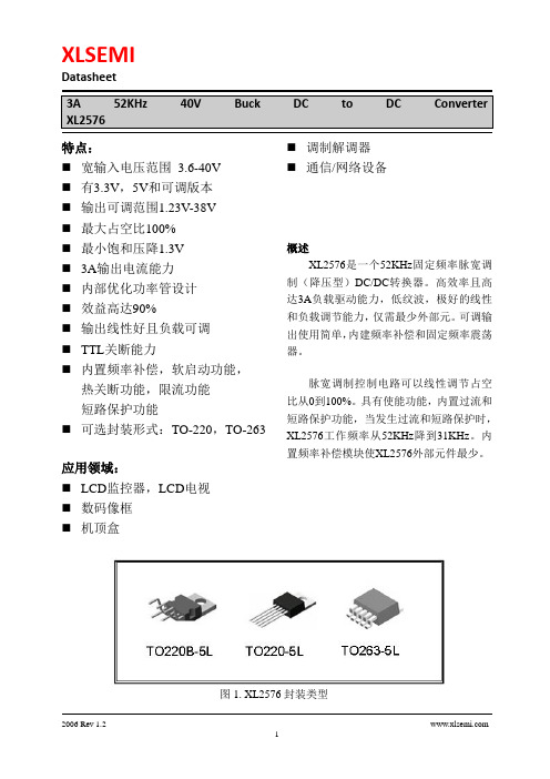
3A 52KHz 40V Buck DC to DC Converter XL2576特点:⏹宽输入电压范围3.6-40V⏹有3.3V,5V和可调版本⏹输出可调范围1.23V-38V⏹最大占空比100%⏹最小饱和压降1.3V⏹3A输出电流能力⏹内部优化功率管设计⏹效益高达90%⏹输出线性好且负载可调⏹TTL关断能力⏹内置频率补偿,软启动功能,热关断功能,限流功能短路保护功能⏹可选封装形式:TO-220,TO-263应用领域:⏹LCD监控器,LCD电视⏹数码像框⏹机顶盒⏹调制解调器⏹通信/网络设备概述XL2576是一个52KHz固定频率脉宽调制(降压型)DC/DC转换器。
高效率且高达3A负载驱动能力,低纹波,极好的线性和负载调节能力,仅需最少外部元。
可调输出使用简单,内建频率补偿和固定频率震荡器。
脉宽调制控制电路可以线性调节占空比从0到100%。
具有使能功能,内置过流和短路保护功能,当发生过流和短路保护时,XL2576工作频率从52KHz降到31KHz。
内置频率补偿模块使XL2576外部元件最少。
图1. XL2576封装类型3A 52KHz 40V Buck DC to DC Converter XL2576引脚设置图2. XL2576引脚结构(顶视图)表格1引脚描述引脚数引脚名描述1 输入电压输入引脚,XL2576工作在直流电压3.6V到40V,外接适合大的旁路电容到地来消除输入噪声。
2 输出功率开关输出引脚(SW).输出端是提供功率输出的开关结点。
3 GND 接地引脚,做版图时必须小心。
此引脚必须放置在硝特基二极管和输出电容到地的外面,来阻止电感电压噪声引起的开关电流毛刺输入到XL2576。
4 反馈反馈引脚(FB),通过外部电阻来分割回路,反馈是来检测和调节输出电压,反馈端电压是1.23V。
5 ON/OFF 使能引脚。
驱动ON/OFF 引脚为低电平则开启设备,驱动此引脚为高电平则关断设备,悬空默认为低电平。
关于MAX6675的说明书
General DescriptionThe MAX6675 performs cold-junction compensation and digitizes the signal from a type-K thermocouple. The data is output in a 12-bit resolution, SPI-compatible, read-only format.This converter resolves temperatures to 0.25°C, allows readings as high as +1024°C, and exhibits thermocouple accuracy of 8 LSBs for temperatures ranging from 0°C to +700°C.The MAX6675 is available in a small, 8-pin SO package.Applications●Industrial ●Appliances ●HVACFeatures●Direct Digital Conversion of Type -K ThermocoupleOutput ●Cold-Junction Compensation●Simple SPI-Compatible Serial Interface ●12-Bit, 0.25°C Resolution ●Open Thermocouple DetectionPART TEMP RANGE PIN-PACKAGE MAX6675ISA-20°C to +85°C8 SOMAX6675Cold-Junction-Compensated K-Thermocouple-to-Digital Converter (0°C to +1024°C)19-2235; Rev 3; 6/21Ordering InformationEVALUATION KIT AVAILABLEClick here to ask about the production status of specific part numbers.Supply Voltage (V CC to GND) ............................... -0.3V to +6V SO, SCK, CS , T-, T+ to GND .....................-0.3V to V CC + 0.3V SO Current ....................................................................... 50mA ESD Protection (Human Body Model) .......................... ±2000V Continuous Power Dissipation (T A = +70°C)8-Pin SO (derate 5.88mW/°C above +70°C) ............. 471mW Operating Temperature Range ..........................-20°C to +85°CStorage Temperature Range ...........................-65°C to +150°C Junction Temperature .................................................... +150°C SO PackageVapor Phase (60s) . .....................................................+215°C Infrared (15s) ..............................................................+220°C Lead Temperature (soldering, 10s) ............................... +300°C(V CC = +3.0V to +5.5V, T A = -20°C to +85°C, unless otherwise noted. Typical values specified at +25°C.) (Note 1)PARAMETERSYMBOLCONDITIONSMINTYP MAX UNITSTemperature ErrorT THERMOCOUPLE = +700°C,T A = +25°C (Note 2)V CC = +3.3V -5+5LSBV CC = +5V -6+6T THERMOCOUPLE = 0°C to +700°C, T A = +25°C (Note 2)V CC = +3.3V -8+8V CC = +5V -9+9T THERMOCOUPLE = +700°Cto +1000°C, T A = +25°C (Note 2)V CC = +3.3V -17+17V CC = +5V-19+19Thermocouple Conversion Constant10.25µV/LSB Cold-JunctionCompensation Error T A = -20°C t o +85°C (Note 2)V CC = +3.3V -3.0+3.0°C V CC= +5V-3.0+3.0Resolution0.25°C Thermocouple Input Impedance 60k W Supply Voltage V CC 3.05.5V Supply CurrentI CC0.7 1.5mA Power-On Reset Threshold V CC rising12 2.5V Power-On Reset Hysteresis 50mV Conversion Time (Note 2)0.170.22sSERIAL INTERFACE Input Low Voltage V IL 0.3 x V CCV Input High Voltage V IH 0.7 x V CCV Input Leakage Current I LEAK V IN = GND or V CC±5µA Input CapacitanceC IN5pFto-Digital Converter (0°C to +1024°C)Electrical CharacteristicsStresses beyond those listed under “Absolute Maximum Ratings” may cause permanent damage to the device. These are stress ratings only, and functional operation of the device at these or any other conditions beyond those indicated in the operational sections of the specifications is not implied. Exposure to absolute maximum rating conditions for extended periods may affect device reliability.Absolute Maximum RatingsNote 1: All specifications are 100% tested at T A = +25°C. Specification limits over temperature (T A = T MIN to T MAX ) are guaranteedby design and characterization, not production tested.Note 2: Guaranteed by design. Not production tested.(V CC = +3.3V, T A = +25°C, unless otherwise noted.)(V CC = +3.0V to +5.5V, T A = -20°C to +85°C, unless otherwise noted. Typical values specified at +25°C.) (Note 1)PARAMETERSYMBOL CONDITIONSMIN TYPMAXUNITS Output High Voltage V OH I SOURCE = 1.6mA V CC - 0.4V Output Low Voltage V OLI SINK = 1.6mA0.4VTIMINGSerial Clock Frequency f SCL 4.3MHz SCK Pulse High Width t CH 100ns SCK Pulse Low Width t C L 100ns CSB Fall to SCK Rise t CSS C L = 10pF 100ns CSB Fall to Output Enable t DV C L = 10pF 100ns CSB Rise to Output Disable t TR C L = 10pF 100ns SCK Fall to Output Data Validt DOC L = 10pF100ns-50510-103050OUTPUT CODE ERROR vs. VOLTAGE DIFFERENTIALM A X 6675 t o c 02VOLTAGE DIFFERENTIAL (mV)O U T P U T C O D E E R R O R (L S B )1020401086420451530607590OUTPUT CODE ERROR vs. AMBIENT TEMPERATUREM A X 6675 t o c 01TEMPERATURE (°C)O U T P U T C O D E E R R O R (L S B )to-Digital Converter (0°C to +1024°C)Typical Operating CharacteristicsElectrical Characteristics (continued)Detailed DescriptionThe MAX6675 is a sophisticated thermocouple-to-digi- tal converter with a built-in 12-bit analog-to-digital con-verter (ADC). The MAX6675 also contains cold-junction compensation sensing and correction, a digital con- troller, an SPI-compatible interface, and associated control logic.The MAX6675 is designed to work in conjunction with an external microcontroller (µC) or other intelligence in ther-mostatic, process-control, or monitoring applications. Temperature ConversionThe MAX6675 includes signal-conditioning hardware to convert the thermocouple’s signal into a voltage compat-ible with the input channels of the ADC. The T+and T- inputs connect to internal circuitry that reduces the intro- duction of noise errors from the thermocouple wires. Before converting the thermoelectric voltages into equivalent temperature values, it is necessary to com-pensate for the difference between the thermocouple cold-junction side (MAX6675 ambient temperature) and a 0°C virtual reference. For a type-K thermocouple, the voltage changes by 41µV/°C, which approximates the thermocouple characteristic with the following linear equation:V OUT = (41µV / °C) x (T R - T AMB)Where:V OUT is the thermocouple output voltage (µV).T R is the temperature of the remote thermocouple junc-tion (°C).T AMB is the ambient temperature (°C).Cold-Junction CompensationThe function of the thermocouple is to sense a differ- ence in temperature between two ends of the thermo- couple wires. The thermocouple’s hot junction can be read from 0°C to +1023.75°C. The cold end (ambi-ent temperature of the board on which the MAX6675 is mounted) can only range from -20°C to +85°C. While the temperature at the cold end fluctuates, the MAX6675 continues to accurately sense the tempera- ture difference at the opposite end.The MAX6675 senses and corrects for the changes in the ambient temperature with cold-junction compen-sation. The device converts the ambient temperature reading into a voltage using a temperature-sensing diode. To make the actual thermocouple temperature measurement, the MAX6675 measures the voltage from the thermocouple’s output and from the sensing diode. The device’s internal circuitry passes the diode’s volt- age (sensing ambient temperature) and thermocouple voltage (sensing remote temperature minus ambient temperature) to the conversion function stored in the ADC to calculate the thermocouple’s hot-junction tem-perature.Optimal performance from the MAX6675 is achieved when the thermocouple cold junction and the MAX6675 are at the same temperature. Avoid placing heat-gen-erating devices or components near the MAX6675 because this may produce cold-junction-related errors. DigitizationThe ADC adds the cold-junction diode measurement with the amplified thermocouple voltage and reads out the 12-bit result onto the SO pin. A sequence of all zeros means the thermocouple reading is 0°C. A sequence of all ones means the thermocouple reading is +1023.75°C.PIN NAME FUNCTION1GND Ground2T-Alumel Lead of Type-K Thermocouple.Should be connected to ground externally. 3T+Chromel Lead of Type-K Thermocouple4V CC Positive Supply. Bypass with a 0.1µFcapacitor to GND.5SCK Serial Clock Input6CS Chip Select. Set CS low to enable the serialinterface.7SO Serial Data Output8N.C.No Connection to-Digital Converter (0°C to +1024°C)Pin DescriptionApplications InformationSerial InterfaceThe T ypical Application Circuit shows the MAX6675 interfaced with a microcontroller. In this example, the MAX6675 processes the reading from the thermocou- ple and transmits the data through a serial interface. Force CS low and apply a clock signal at SCK to read the results at SO. Forcing CS low immediately stops any conversion process. Initiate a new conversion process by forcing CS high.Force CS low to output the first bit on the SO pin. A complete serial interface read requires 16 clock cycles. Read the 16 output bits on the falling edge of the clock. The first bit, D15, is a dummy sign bit and is always zero. Bits D14–D3 contain the converted temperature in the order of MSB to LSB. Bit D2 is normally low and goes high when the thermocouple input is open. D1 is low to provide a device ID for the MAX6675 and bit D0 is three-state.Figure 1a is the serial interface protocol and Figure 1b shows the serial interface timing. Figure 2 is the SO out-put.Open ThermocoupleBit D2 is normally low and goes high if the thermocou- ple input is open. In order to allow the operation of the open thermocouple detector, T- must be grounded. Make the ground connection as close to the GND pin as possible.Noise ConsiderationsThe accuracy of the MAX6675 is susceptible to power- supply coupled noise. The effects of power-supply noise can be minimized by placing a 0.1µF ceramic bypass capacitor close to the supply pin of the device.Thermal ConsiderationsSelf-heating degrades the temperature measurement accuracy of the MAX6675 in some applications. The magnitude of the temperature errors depends on the thermal conductivity of the MAX6675 package, the mounting technique, and the effects of airflow. Use a large ground plane to improve the temperature mea- surement accuracy of the MAX6675.The accuracy of a thermocouple system can also be improved by following these precautions:●Use the largest wire possible that does not shuntheat away from the measurement area.●If small wire is required, use it only in the region ofthe measurement and use extension wire for theregion with no temperature gradient.●Avoid mechanical stress and vibration, which couldstrain the wires.●When using long thermocouple wires, use a twisted-pair extension wire.●Avoid steep temperature gradients.●Try to use the thermocouple wire well within its tem-perature rating.●Use the proper sheathing material in hostile environ-ments to protect the thermocouple wire.●Use extension wire only at low temperatures andonly in regions of small gradients.●Keep an event log and a continuous record of ther-mocouple resistance.Reducing Effects of Pick-Up NoiseThe input amplifier (A1) is a low-noise amplifier designed to enable high-precision input sensing. Keep the thermocouple and connecting wires away from elec-trical noise sources.to-Digital Converter (0°C to +1024°C)Figure 2. SO OutputFigure 1b. Serial Interface TimingFigure 1a. Serial Interface ProtocolBIT DUMMY SIGN BIT12-BITTEMPERATURE READING THERMOCOUPLEINPUTDEVICE IDSTATE Bit15141312111098765432100MSBLSBThree-stateCSSCKSOD15D14D13D12D11D10D9D8D7D6D5D4D3D2D1D0to-Digital Converter (0°C to +1024°C)PACKAGE TYPEPACKAGE CODE OUTLINE ND PATTERN NO.8 SOS8+221-004190-0096to-Digital Converter (0°C to +1024°C)Package InformationFor the latest package outline information and land patterns (footprints), go to /packages . Note that a “+”, “#”, or “-” in the package code indicates RoHS status only. Package drawings may show a different suffix character, but the drawing pertains to the package regardless of RoHS status.Chip InformationTRANSISTOR COUNT: 6720PROCESS: BiCMOSREVISION NUMBERREVISION DATE DESCRIPTIONPAGES CHANGED24/14Removed automotive reference136/21Updated equation in Temperature Compensation section.4Maxim Integrated cannot assume responsibility for use of any circuitry other than circuitry entirely embodied in a Maxim Integrated product. No circuit patent licenses are implied. Maxim Integrated reserves the right to change the circuitry and specifications without notice at any time. The parametric values (min and max limits) shown in the Electrical Characteristics table are guaranteed. Other parametric values quoted in this data sheet are provided for guidance.to-Digital Converter (0°C to +1024°C)Revision HistoryFor pricing, delivery, and ordering information, please visit Maxim Integrated’s online storefront at https:///en/storefront/storefront.html.。