5962-9220303MRA中文资料
3M VHB 胶带 物性表
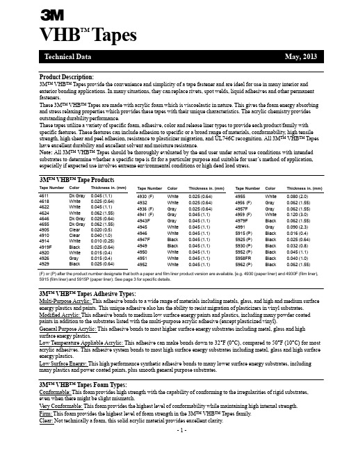
Tape NumberColorThickness in. (mm)Tape NumberColorThickness in. (mm)4930 (F) White 0.025 (0.64) 4955 White 0.080 (2.0) 4932 White 0.025 (0.64) 4956 (F) Gray 0.062 (1.55) 4936 (F) Gray 0.025 (0.64) 4957F Gray 0.062 (1.55) 4941 (F) Gray 0.045 (1.1) 4959 (F) White 0.120 (3.0) 4943F Gray 0.045 (1.1) 4979F Black 0.062 (1.55) 4945 White 0.045 (1.1) 4991 Gray 0.090 (2.3) 4946 White 0.045 (1.1) 5915 (P) Black 0.016 (0.4) 4947F Black 0.045 (1.1) 5925 (P) Black 0.025 (0.64) 4949 Black 0.045 (1.1) 5930 (P) Black 0.032 (0.8) 4950 White 0.045 (1.1) 5952 (P) Black 0.045 (1.1) 4951 White 0.045 (1.1) 5958FR Black 0.040 (1.0) 4952 White 0.045 (1.1)5962 (P) Black 0.062 (1.55)VHB ™T apesTechnical DataMay, 2013Product Description:3M ™ VHB ™ Tapes provide the convenience and simplicity of a tape fastener and are ideal for use in many interior and exterior bonding applications. In many situations, they can replace rivets, spot welds, liquid adhesives and other permanent fasteners.These 3M ™ VHB ™ Tapes are made with acrylic foam which is viscoelastic in nature. This gives the foam energy absorbing and stress relaxing properties which provides these tapes with their unique characteristics. The acrylic chemistry provides outstanding durability performance.These tapes utilize a variety of specific foam, adhesive, color and release liner types to provide each product/family with specific features. These features can include adhesion to specific or a broad range of materials, conformability, high tensile strength, high shear and peel adhesion, resistance to plasticizer migration, and UL746C recognition. All 3M ™ VHB ™ Tapes have excellent durability and excellent solvent and moisture resistance.Note: All 3M ™ VHB ™ Tapes should be thoroughly evaluated by the end user under actual use conditions with intended substrates to determine whether a specific tape is fit for a particular purpose and suitable for user ’s method of application, especially if expected use involves extreme environmental conditions or high dead load stress.3M ™ VHB ™ T ape ProductsTape NumberColorThickness in. (mm)4611 Dk Gray 0.045 (1.1) 4618 White 0.025 (0.64) 4622 White 0.045 (1.1) 4624 White 0.062 (1.55) 4646 Dk Gray 0.025 (0.64) 4655 Dk Gray 0.062 (1.55) 4905 Clear 0.020 (0.5) 4910 Clear 0.040 (1.0) 4914 White 0.010 (0.25) 4919F Black 0.025 (0.64) 4920 White 0.015 (0.4) 4926 Gray 0.015 (0.4) 4929 Black 0.025 (0.64) (F) or (P) after the product number designate that both a paper and film liner product version are available. [e.g. 4930 (paper liner) and 4930F (film liner),5915 (film liner) and 5915P (paper liner). See page 3 for specific details.3M ™ VHB ™ Tapes Adhesive Types:Multi-Purpose Acrylic: This adhesive bonds to a wide range of materials including metals, glass, and high and medium surface energy plastics and paints. This unique adhesive also has the ability to resist migration of plasticizers in vinyl substrates. Modified Acrylic: This adhesive bonds to medium low surface energy paints and plastics, including many powder coated paints in addition to the substrates listed with the multi-purpose acrylic adhesive (except plasticized vinyl).General Purpose Acrylic: This adhesive bonds to most higher surface energy substrates including metal, glass and high surface energy plastics.Low Temperature Appliable Acrylic: This adhesive can make bonds down to 32°F (0°C), compared to 50°F (10°C) for most acrylic adhesives. This adhesive system bonds to most high surface energy substrates including metal, glass and high surface energy plastics.Low Surface Energy: This high performance synthetic adhesive bonds to many lower surface energy substrates, including many plastics and power coated paints, plus smooth general purpose substrates.3M ™ VHB ™ Tapes Foam Types:Conformable: This foam provides high strength with the capability of conforming to the irregularities of rigid substrates, even when there might be slight mismatch.Very Conformable: This foam provides the highest level of conformability while maintaining high internal strength. Firm: This foam provides the highest level of foam strength in the 3M ™ VHB ™ Tapes family. Clear: Not technically a foam, this solid acrylic material provides excellent clarity.3M™VHB™Tapes3M™ VHB™ Tape Families:4941 This family utilizes multi-purpose acrylic adhesive on both sides of conformable foam. The adhesive provides excellent adhesion to a broad range of high and medium surface energy substrates including metals, glass, and awide variety of plastics, as well as plasticized vinyl. The conformable foam provides good contact, even withmismatched substrates. Available in gray and black.5952 This family matches the modified acrylic adhesive on both sides of very conformable foam, providing adhesion to the broadest range of substrates, including most powder coated paints. Available in black.4950 This family has general purpose adhesive on both sides of firm type foam. This family is typically used on metal, glass and high surface energy plastic substrates. Available in white and black.4945 This family has multi-purpose adhesive on both sides of firm foam. Available in white.4910 This family of clear tapes is excellent for applications where clear or colorless is desired. The general purpose adhesive on both sides is suitable for high surface energy substrates.4951 This family of tapes is based around the low temperature appliable acrylic adhesive system, utilized on both firm and conformable foam types. These products are suitable for high surface energy substrates. Available inwhite (firm foam) and gray (conformable foam).4952 This family utilizes the low surface energy adhesive on a firm foam. Available in white.4611 This family has a general purpose adhesive on both sides of firm foam. This family of tapes is typically used on metal substrates, and has the added feature of high temperature resistance, making it often suitable for bondingprior to high temperature paint processing. Available in dark gray.4622 This family has general purpose adhesive on the face side (the side that typically would be bonded first) and multi-purpose adhesive on the liner side (the side exposed when the release liner is removed) of a conformablefoam. Available in white.3M™ VHB™ Tape Product Family GuideNOTE: For easy product comparison, data in this product information page will be organized by product family.3M ™ VHB ™ TapesTypical Physical PropertiesNote: The following technical information and data should be consideredrepresentative or typical only and should not be used for specification purposes.3M ™ VHB ™ TapesTypical Performance CharacteristicsNote: The following technical information and data should be consideredrepresentative or typical only and should not be used for specification purposes.90° Peel Adhesion - Based on ASTM D3330 -T o stainless steel, room temperature, jaw speed 12 in/min (305 mm/min). Average force to remove is measured. 72 hour dwell.Normal Tensile (T-Block T ensile) - ASTM D-897 - T o aluminum, room temperature, 1 in 2 (6.45 cm 2), jaw speed 2 in/min (50 mm/min.) Peak force to separate is measured. 72 hour dwell.Dynamic Overlap Shear - ASTM D-1002 - T o stainless steel, room temperature, 1 in 2 (6.45 cm 2), jaw speed 0.5 in/min (12.7 mm/min.) Peak force to separate is measured. 72 hour dwell.3M ™ VHB ™ TapesTypical Performance CharacteristicsNote: The following technical information and data should be consideredrepresentative or typical only and should not be used for specification purposes.Static Shear - ASTM D3654 - To stainless steel, tested at various temperatures and gram loadings. 0.5 in 2 (3.22 cm 2). Will hold listed weight for 10,000 minutes (approximately 7 days). Conversion: 1500 g/0.5 in 2 equals 6.6 lb/in 2; 500 g/0.5 in 2 = 2.2 lb/in 2.Short Term Temperature Tolerance - No change in room temperature dynamic shear properties following 4 hours conditioning at indicated temperature with 100 g/static load. (Represents minutes, hours in a process type temperature exposure).Long Term Temperature Tolerance - Maximum temperature where tape supports at least 250 g load per 0.5 in 2 in static shear for 10,000 minutes. (Represents continuous exposure for days or weeks).3M™VHB™Tapes*Exception – 5915 (P) max. width 46 inches (1170 mm); 5925 (P) max. width 47 inches (1195 mm).Slitting T oleranceStandard slitting tolerance ± 1/32 inch (± 0.031 inch, ± 0.8 mm).Precision slitting with slitting tolerance of ± 1/64 inch (± 0.016 in., ± 0.44 mm) is available on select products with minimum order of full web increments.Core SizeAll products are provided on a 3 inch ID Core (76.2 mm).Converted PartsIn addition to standard and custom roll sizes available from 3M through the distribution network, 3M™VHB™ Tapes are also available in limitless shapes and sizes through the 3M Converter network. For additional information, contact 3M Converter Markets at 1-800-223-7427 or on the web at /converter.Shelf LifeAll 3M™VHB™ Tapes have a shelf life of 24 months from date of manufacture when stored at 40°F to 100°F (4°C to 38°C) and 0-95% relative humidity. The optimum storage conditions are 72°F (22°C) and 50% relative humidity.Performance of tapes is not projected to change even after shelf life expires; however, 3M does suggest that3M™VHB™ Tapes are used prior to the shelf life date whenever possible.The manufacturing date is available on all 3M™VHB™ Tape cores as the lot number. The lot number, typically a 4 digit code, is a Julian date (Y D D D). The first digit refers to the year of manufacture, the last 3 digits refer to the days after January 1. Example: A lot number of 9266 would translate to a date of manufacture of Sept. 22 (266th day of year) in 2009. On most products this is found as the 4 digits after the “9” following the product number. For tapes printed continuously around the core (e.g. 3M™VHB™ Tape 5952 family) the lot number typically will be the string of 4 digits preceding the product number.3M ™ VHB ™ TapesTapesConstant Factor 4941 at 1 kHz2.29 0.0245 Tapes 4941 hr ft °F 0.53 (w/mK) (0.08) 5952 0.37 (0.05) at 1 MHz 1.95 0.0506 4950/4945 0.63 (0.09) 4950 at 1 kHz 2.28 0.0227 4910 1.09 (0.16) at 1 MHz 1.99 0.0370 46110.77(0.11)5952 at 1 kHz2.14 0.00654910 at 1 kHz 3.21 0.0214 at 1 MHz 2.68 0.0595 4611 at 1 kHz 2.80 0.0130 at 1 MHz2.430.0564nAdditional Typical Performance CharacteristicsNote: The following technical information and data should be considered representative or typical only and should notbe used for specification purposes.Outgassing: 3M ™ VHB™ Tapes % TML %VCM %WVR Dielectric Breakdown Strength (ASTM D149)3M ™ VHB™ Tapes (in volts/mil)3M ™ VHB ™ TapesUL746C Listings - File MH 17478Category QOQW2 Component - Polymeric Adhesive Systems, Electrical Equipment4930 0.77 0.01 0.214932 2.41 0.66 0.23 49451.240.010.19TML - Total Mass LossVCM - Volatile Condensible Materials WVR - Water Vapor RegainedNASA Reference Publication, “Outgassing Data for Selecting Spacecraft Materials”, (11/18/2004) Available online at 4941 360 4926 330 5952 455 5925 520 4950 460 4920 640 4910 630 4611330Dielectric Constant (ASTM D150) 3M ™ VHB ™ Dielectric DissipationThermal Conductivity - K-value 3M™ VHB™ BTU in/at 1 MHz1.990.0374Resistivity (ASTM D257)R-Value = thicknessK-value(When units of K-value are BTU-in/hr ft °F and thickness is given in inches.)3M ™ VHB ™ Volume Resistivity Surface Resistance Tapes (in ohm-cm)(in ohms/square)4914 1.7 x 10>104941 2.1 x 10 2.7 x 105952 2.5 x 10>10 4950 1.5 x 10>10 4920 1.7 x 10>10 4910 3.1 x 10>10 46111.4 x 10>10Water Vapor Transmission Rate (WVTR) (ASTM F1249) at 38°C/100% RH 3M ™ VHB ™ Tapes 4950 14.0 g/(m 2 day) 4941 25.6 g/(m 2 day) 595237.1 g/(m 2 day)Solvent and Fuel ResistanceTypical 3M ™ VHB ™ Tape Properties for Modeling %R100 90 Thermal Coefficient Ae 8080 of Expansion1 x 10in/in/°F1.8 x 10mm/mm/°C Shear Modulus (@25°C, 1 Hz)d t 7070 he 6060 en 5050 s t 4040 i i 3030 4950 Family: 6 x 10Pa 4941 Family: 3 x 10Pa(Shear Modulus is both temperature and frequency dependent).Youngs Modulus: For VHB tapes the YoungsModulus will be about 3 times the Shear Modulus. v o 20e Salt WaterHydraulic Fluid10W30 Motor Oil KeroseneIsopropyl AlcoholJet Fuel20 10 0Poisson ’s Ratio T est MethodGlycol Antifreeze0.49Burn Characteristics 3M ™ VHB ™ Tape 5958FR Meets FAR 25.853 (a) 12 second vertical burn, Appendix F, Part I (a)(ii).Meets NBS Smoking Density (ASTM F814/E662). Meets Toxicity (Draeger Tube ABD0031, AITM 3.0005)• T ape between stainless steel and aluminum foil. • 72 hours dwell at room temperature. • Solvent immersion for 72 hours.• T est within 45 minutes after removing from solvent. • 90° peel angle.• 12 in./min. rate of peel.• Peel adhesion compared to control.Note: Continuous submersion in chemical solutions is not recommended. The above information is presented to show thatoccasional chemical contact should not be detrimental to tape performance in most applications in ordinary use.3M ™ VHB ™ TapesE s t i m a t e o f % o f M a x i m u m 3M ™ V H B ™ T a p e A d h e s i o nDesign and T ape Selection ConsiderationsChoose the right tape for the substrate: Adhesives must flow onto the substrate surfaces in order to achieve intimate contact area and allow the molecular force of attraction to develop. The degree of flow of the adhesive on the substrate is largely determined by the surface energy of the substrate.AdhesiveHigh surface energy— SubstrateLow surface energy— SubstrateThis illustration demonstrates the effect of surface energy on adhesive interfacial contact. High surface energy materials draw the adhesive closer for high bond strength.Relationship of Adhesion and Surface Energy for 3M ™ VHB ™ Tape Adhesive FamiliesHIGHMEDIUMLOW400-1100 Aluminum42-50 PolyimideABS38-39PVA36-37EVA18-33 Stainless Steel Copper Zinc Tin LeadAnodized Aluminum GlassPhenolic NylonAlkyd Enamel Polyester Epoxy Paint PolyurethanePolycarbonate (Lexan ®) PVC Noryl ® AcrylicPolane ® Paint Powder PaintPolystyrene AcetalKynar ® Paint Powder PaintPolyethylene Polypropylene Tedlar ® Silicone PTFENOTES: There are a wide variety of formulations, surfaces finishes and surface treatments available on substrate materials which can affect adhesion. This chart is intendedto provide only a rough estimate of the adhesion levels which can be expected on some common materials relative to a reference surface such as aluminum.Light abrasion of surface will significantly increase adhesion levels on many materials, except when using tapes 4952/4932.Use the right tape thickness: The necessary thickness of tape depends on the rigidity of substrates and their flatness irregularity. While the 3M ™ VHB ™ Tapes will conform to a certain amount of irregularity, they will not flow to fill gaps between the materials. For bonding rigid materials with normal flatness, consider use of tapes with thickness of 45 mils (1.1 mm) or greater. As the substrate flexibility increases thinner tapes can be considered.Use the right amount of tape: Because 3M ™ VHB ™ Tapes are viscoelastic by nature their strength and stiffness is a function of the rate at which they are stressed. They behave stronger with relatively faster rate of stress load (dynamic stresses) and will tend to show creep behavior with stress load acting over a long period of time (static stresses). As a general rule, for static loads, approximately four square inches of tape should be used for each pound of weight to be supported in order to prevent excessive creep. For dynamic loads, the dynamic performance characteristics provided on page 4 should be useful, factoring in the appropriate safety factors.Allow for thermal expansion/contraction: 3M ™ VHB ™ Tapes can perform well in applications where two bonded surfaces may expand and contract differentially. Assuming good adhesion to the substrates, the tapes can typically tolerate differential movement in the shear plane up to 3 times their thickness.Bond Flexibility: While an advantage for many applications where allowing differential movement is a benefit, the tape bonds are typically more flexible than alternative bonding methods. Suitable design modifications or periodic use of rigid fasteners or adhesives may be needed if additional stiffness is required.Severe Cold Temperature: Applications which require performance at severe cold temperatures must be thoroughly evaluated by the user if the intended use will subject the tape product to high impact stresses. A technical bulletin “3M™ VHB ™ Tape Cold Temperature Performance ” (70-0707-3991-0) is available for additional information.3M ™ VHB ™ TapesApplication T echniquesClean: Most substrates are best prepared by cleaning with a 50:50 mixture of isopropyl alcohol (IPA*) and water prior to applying 3M™ VHB™ Tapes.Exceptions to the general procedure that may require additional surface preparation include:• Heavy Oils: A degreaser or solvent-based cleaner may be required to remove heavy oil or grease from a surface and should be followed by cleaning with IPA/water.• Abrasion: Abrading a surface, followed by cleaning with IPA/water, can remove heavy dirt or oxidation and can increase surface area to improve adhesion.• Adhesion Promoters: Priming a surface can significantly improve initial and ultimate adhesion to many materials such as plastics and paints.• Porous surfaces: Most porous and fibered materials such as wood, particleboard, concrete, etc. need to be sealed to provide a unified surface.• Unique Materials: Special surface preparation may be needed for glass and glass-like materials, copper and copper containing metals, and plastics or rubber that contain components that migrate (e.g. plasticizers).Refer to 3M Technical Bulletin “Surface Preparation for 3M™ VHB™ Tape Applications” for additional details and suggestions. (70-0704-8701-5)*Note: These cleaner solutions contain greater than 250 g/l of volatile organic compounds (VOC). Pleaseconsult your local Air Quality Regulations to be sure the cleaner is compliant. When using solvents, be sure to follow the manufacturer ’s precautions and directions for use when handling such materials.Pressure: Bond strength is dependent upon the amount of adhesive-to-surface contact developed. Firmapplication pressure develops better adhesive contact and helps improve bond strength. Typically, good surface contact can be attained by applying enough pressure to insure that the tape experiences approximately 15 psi (100 kPa) pressure. Either roller or platen pressure can be used. Note that rigid surfaces may require 2 or 3 times that much pressure to make the tape experience 15 psi.Temperature: Ideal application temperature range is 70°F to 100°F (21°C to 38°C). Pressure sensitiveadhesives use viscous flow to achieve substrate contact area. Minimum suggested application temperatures:• 50°F (10°C): 3M™ VHB™ Tapes 4950, 5952, 4910, 4952, 4611, 4622 families. • 60°F (15°C): 3M™ VHB™ Tapes 4941, 4945 families. • 32°F (0°C): 3M ™ VHB ™ Tape 4951 families.Note: Initial tape application to surfaces at temperatures below these suggested minimums is notrecommended because the adhesive becomes too firm to adhere readily. However, once properly applied, low temperature holding is generally satisfactory. To obtain good performance with all 3M™ VHB™ Tapes, it is important to ensure that the surfaces are dry and free of condensed moisture.Time: After application, the bond strength will increase asthe adhesive flows onto the surface (also referred to as “we t out”). Bond Typical Build vs. TimeAt room temperature approximately 50% of ultimate bond strength will be achieved after 20 minutes, 90% after 24 hours 80and 100% after 72 hours. This flow is faster at higher temperatures and slower at lower temperatures. Ultimate bond strength can be achieved more quickly (and in some cases bond strength can be increased) by exposure of the bond to elevated temperatures (e.g. 150°F [66°C] for 1 hour). This can provide better adhesive wetout onto the substrates. Abrasion of the surfaces or the use of primers/ adhesion promoters can also have the effect of increasing bond strength and achieving ultimate bond strength more quickly.20 MIN 1 HOUR24 HOURS3M ™ VHB ™ TapesSpecial Cases:Rough Surfaces with 3M™ VHB™ Tapes 4932/4952 – 3M™ VHB™ Tapes 4932/4952 were designed to adhere to many low surface energy substrates. Rough surfaces created by light abrasion or textured molds are typically detrimental to bond strength with this tape family.Plasticized Vinyl – Plasticizers compounded in soft vinyl can migrate into adhesives and significantly change their performance characteristics. 3M™ VHB™ Tapes 4941 and 4945 families have very good plasticizer resistance and adhesion to many vinyl formulations. Because of the wide variation in vinyl formulations,however, evaluation by the user must be conducted with the specific vinyl used to ensure that performance will be satisfactory over time. Problems related to plasticizer migration can often be predicted by accelerated aging of assembled parts at 150°F (66°C) for one week).Technical InformationThe technical information, recommendations and other statements contained in this document arebased upon tests or experience that 3M believes are reliable, but the accuracy or completeness of such information is not guaranteed.Product UseMany factors beyond 3M ’s control and uniquely within user ’s knowledge and control can affect the use and performance of a 3M product in a particular application. Given the variety of factors that can affect the use and performance of a 3M product, user is solely responsible for evaluating the 3M product and determining whether it is fit for a particular purpose and suitable for user ’s method of application.Limited Warranty3M warrants for 24 months from the date of manufacture that 3M™ VHB™ Tape will be free of defects in material and manufacture. 3M MAKES NO OTHER WARRANTIES, EXPRESS OR IMPLIED, INCLUDING BUT NOT LIMITED TO, ANY IMPLIED WARRANTY OF MERCHANTABILITY OR FITNESS FOR A PARTICULAR PURPOSE. This limited warranty does not cover damage resulting from the use or inability to use 3M ™ VHB™ Tape due to misuse, workmanship in application, or application or storage not in accordance with 3M recommended procedures. AN APPLICATIONWARRANTY EXPRESSLY APPROVED AND ISSUED BY 3M IS AN EXCEPTION. THE CUSTOMER MUST APPLY FOR A SPECIFIC APPLICATION WARRANTY AND MEET ALL WARRANTY ANDPROCESS REQUIREMENTS TO OBTAIN AN APPLICATION WARRANTY . CONTACT 3M FOR MORE INFORMATION ON APPLICATION WARRANTY TERMS AND CONDITIONS.Limitation of Remedies and LiabilityIf the 3M ™ VHB ™ T ape is proved to be defective within the warranty period stated above. THE EXCLUSIVE REMEDY , AT 3M’S OPTION, SHALL BE TO REFUND THE PURCHASE PRICE OF OR TO REPAIR OR REPLACE THE DEFECTIVE 3M ™ VHB ™ TAPE. 3M shall not otherwise be liable for loss or damages, whether direct, indirect, special, incidental, or consequential, regardless of the legal theory asserted, including negligence, warranty, or strict liability.This Industrial Adhesives and Tapes Division product was manufactured under a 3M quality system registered to ISO 9001: 2008 standards.Industrial Adhesives and Tapes Division3M Center, Building 225-3S-06 St. Paul, MN 55144-1000800-362-3550 • 877-369-2923 (Fax) /vhbRecycled Paper 40% pre-consumer 10% post-consumer3M and VHB are trademarks of 3M Company. Tedlar is a registered trademark of E.I. Dupont De Nemours & Co. Inc.Kynar is a registered trademark of Arkema.Lexan and Noryl are registered trademarks of Sabic Innovative Plastics IP BV.Polane is a registered trademark of Swimc, Inc. Printed in U.S.A.©3M 2013 70-0709-3863-7(6/11)。
5962-9322001Q2A资料

PACKAGING INFORMATIONOrderable Device Status(1)PackageType PackageDrawingPins PackageQtyEco Plan(2)Lead/Ball Finish MSL Peak Temp(3)5962-9322001Q2A ACTIVE LCCC FK201None Call TI Level-NC-NC-NC 5962-9322001QRA ACTIVE CDIP J201None Call TI Level-NC-NC-NC 5962-9322001QSA ACTIVE CFP W201None Call TI Level-NC-NC-NC SN74ABT574ADBLE OBSOLETE SSOP DB20None Call TI Call TISN74ABT574ADBR ACTIVE SSOP DB202000Pb-Free(RoHS)CU NIPDAU Level-2-260C-1YEAR/Level-1-235C-UNLIMSN74ABT574ADW ACTIVE SOIC DW2025Pb-Free(RoHS)CU NIPDAU Level-2-250C-1YEAR/Level-1-235C-UNLIMSN74ABT574ADWR ACTIVE SOIC DW202000Pb-Free(RoHS)CU NIPDAU Level-2-250C-1YEAR/Level-1-235C-UNLIMSN74ABT574AGQNR ACTIVE VFBGA GQN201000None SNPB Level-1-240C-UNLIM SN74ABT574AN ACTIVE PDIP N2020Pb-Free(RoHS)CU NIPDAU Level-NC-NC-NCSN74ABT574ANSR ACTIVE SO NS202000Pb-Free(RoHS)CU NIPDAU Level-2-260C-1YEAR/Level-1-235C-UNLIMSN74ABT574APW ACTIVE TSSOP PW2070Pb-Free(RoHS)CU NIPDAU Level-1-250C-UNLIMSN74ABT574APWLE OBSOLETE TSSOP PW20None Call TI Call TISN74ABT574APWR ACTIVE TSSOP PW202000Pb-Free(RoHS)CU NIPDAU Level-1-250C-UNLIMSN74ABT574ARGYR ACTIVE QFN RGY201000Green(RoHS&no Sb/Br)CU NIPDAU Level-2-260C-1YEARSN74ABT574AZQNR ACTIVE VFBGA ZQN201000Pb-Free(RoHS)SNAGCU Level-1-260C-UNLIM SNJ54ABT574FK ACTIVE LCCC FK201None Call TI Level-NC-NC-NC SNJ54ABT574J ACTIVE CDIP J201None Call TI Level-NC-NC-NC SNJ54ABT574W ACTIVE CFP W201None Call TI Level-NC-NC-NC (1)The marketing status values are defined as follows:ACTIVE:Product device recommended for new designs.LIFEBUY:TI has announced that the device will be discontinued,and a lifetime-buy period is in effect.NRND:Not recommended for new designs.Device is in production to support existing customers,but TI does not recommend using this part in a new design.PREVIEW:Device has been announced but is not in production.Samples may or may not be available.OBSOLETE:TI has discontinued the production of the device.(2)Eco Plan-May not be currently available-please check /productcontent for the latest availability information and additional product content details.None:Not yet available Lead(Pb-Free).Pb-Free(RoHS):TI's terms"Lead-Free"or"Pb-Free"mean semiconductor products that are compatible with the current RoHS requirements for all6substances,including the requirement that lead not exceed0.1%by weight in homogeneous materials.Where designed to be soldered at high temperatures,TI Pb-Free products are suitable for use in specified lead-free processes.Green(RoHS&no Sb/Br):TI defines"Green"to mean"Pb-Free"and in addition,uses package materials that do not contain halogens, including bromine(Br)or antimony(Sb)above0.1%of total product weight.(3)MSL,Peak Temp.--The Moisture Sensitivity Level rating according to the JEDECindustry standard classifications,and peak solder temperature.Important Information and Disclaimer:The information provided on this page represents TI's knowledge and belief as of the date that it is provided.TI bases its knowledge and belief on information provided by third parties,and makes no representation or warranty as to the accuracy of such information.Efforts are underway to better integrate information from third parties.TI has taken and continues to takereasonable steps to provide representative and accurate information but may not have conducted destructive testing or chemical analysis on incoming materials and chemicals.TI and TI suppliers consider certain information to be proprietary,and thus CAS numbers and other limited information may not be available for release.In no event shall TI's liability arising out of such information exceed the total purchase price of the TI part(s)at issue in this document sold by TIto Customer on an annual basis.元器件交易网IMPORTANT NOTICETexas Instruments Incorporated and its subsidiaries (TI) reserve the right to make corrections, modifications,enhancements, improvements, and other changes to its products and services at any time and to discontinueany product or service without notice. Customers should obtain the latest relevant information before placingorders and should verify that such information is current and complete. All products are sold subject to TI’s termsand conditions of sale supplied at the time of order acknowledgment.TI warrants performance of its hardware products to the specifications applicable at the time of sale inaccordance with TI’s standard warranty. T esting and other quality control techniques are used to the extent TIdeems necessary to support this warranty. Except where mandated by government requirements, testing of allparameters of each product is not necessarily performed.TI assumes no liability for applications assistance or customer product design. Customers are responsible fortheir products and applications using TI components. T o minimize the risks associated with customer productsand applications, customers should provide adequate design and operating safeguards.TI does not warrant or represent that any license, either express or implied, is granted under any TI patent right,copyright, mask work right, or other TI intellectual property right relating to any combination, machine, or processin which TI products or services are used. Information published by TI regarding third-party products or servicesdoes not constitute a license from TI to use such products or services or a warranty or endorsement thereof.Use of such information may require a license from a third party under the patents or other intellectual propertyof the third party, or a license from TI under the patents or other intellectual property of TI.Reproduction of information in TI data books or data sheets is permissible only if reproduction is withoutalteration and is accompanied by all associated warranties, conditions, limitations, and notices. Reproductionof this information with alteration is an unfair and deceptive business practice. TI is not responsible or liable forsuch altered documentation.Resale of TI products or services with statements different from or beyond the parameters stated by TI for thatproduct or service voids all express and any implied warranties for the associated TI product or service andis an unfair and deceptive business practice. TI is not responsible or liable for any such statements.Following are URLs where you can obtain information on other Texas Instruments products and applicationsolutions:Products ApplicationsAmplifiers Audio /audioData Converters Automotive /automotiveDSP Broadband /broadbandInterface Digital Control /digitalcontrolLogic Military /militaryPower Mgmt Optical Networking /opticalnetworkMicrocontrollers Security /securityTelephony /telephonyVideo & Imaging /videoWireless /wirelessMailing Address:Texas InstrumentsPost Office Box 655303 Dallas, Texas 75265Copyright 2005, Texas Instruments Incorporated。
瓦茨工业公司检验阀技术数据表说明书
Check valves Technical Data Sheet2CS - SeriesPage 3WI - SeriesPage 3CO - SeriesPages 4 and 5FI - SeriesPages 6 and 7FO - SeriesPages 6 and 7FW - SeriesPages 6 and 7IN - SeriesPages 8 and 9IO - SeriesPages 10 and 11WM - SeriesPages 12 and 13IW - SeriesPage 14TO - SeriesPage 14AuxiliaryMountingToolsPage 15 Summary3Tfit!Other diameters on request.Mounting dimensionsProduct dimensionsO-ringflow (m /h)100908070605040302010d e l t a P (k P a )flow (m /h)100908070605040302010d e l t a P (k P a )4Ø CØ DØ EØ GAll dimensions are given in mm.The Watts check valves type CO with unique sealing principle offers outstanding performances.These check valves are used in plumbing fittings, sanitary taps and in threaded non-return valves where building codes and international standards are required.Other diameters on request.Approvals: K iwa (NL), Belgaqua (B), DVGW (D), NF - ACS (F),WRAS (UK), ETA - GDV (DK), SITAC (S), NSF (US).5100908070605040302010d e l t a P (k P a )Pressure loss-curveClassical guiding of valve stem Guiding of valve stem (WATTS)Some vibrations can occur at low flow rates (water flush atThanks to the unique guide system by slotted stem that eliminates the possibility of movement and optimal hydraulic profile, vibrations are eliminated.By providing this guidance without the possibility of move-ment avoids calcareous deposits and vibration, ensuring a flawless and quiet operation for years.6FI015 DN15FI - FO - FWThe Watts check valve type FI, FO and FW is a perfect slide-in cartridge with added advantages.The best performance in those inlet sides where tightening has to be simple. It is marked by its unique construction and its uni-versal applications.Approvals: K iwa (NL), Belgaqua (B),DVGW (D), NF - ACS (F), NSF (US).FI010 DN8FO015 DN15FO020 DN20FW010 DN10Approval: GDV (DK)7FI010 DN8FI015 DN150.40.81.21.62.02.42.83.23.64.04.85.66.47.28flow (m 3/h)100908070605040302010d e l t a P (k P a )Pressure loss-curveAll dimensions are given in mm.The Watts snap-in valve type IN is a compact and therefore easy to install check valve.The advantage for OEM applications is, that in case of a side- connection in the housing, the O-ring can be mounted first and secondly the check valve itself.This way the O-ring will not be damaged by the sharp edges of the side- connection.This check valve will meet all quality requirements.Its advantages are yours.Approvals: K iwa (NL), Belgaqua (B), DVGW (D), NF - ACS (F),WRAS (UK), ETA - GDV (DK), SITAC (S), NSF (US), AWQC (AUS).All dimensions are given in mm.92468101214161820flow (m 3/h)100908070605040302010Pressure loss-curve d e l t a P (k P a )IN025 - DN25IN032 - DN322468101214161820flo100908070605040302010Pressure loss-curved e l t a P (k P a )IN025 - DN25IN032 - DN320.81.62.43.24.04.85.66.47.28.0flow (m 3/h)100908070605040302010Pressure loss-curve d e l t a P (k P a )IN015 - DN15IN020 - DN200.81.62.43.24.04.85.66.47.28.0flo100908070605040302010Pressure loss-curved e l t a P (k P a )IN015 - DN15IN020 - DN208162432404856647280flow (m 3/h)100908070605040302010Pressure loss-curved e l t a P (k P a )IN040 - DN40IN050 - DN5008162432404856647280f100908070605040302010Pressure loss-curved e l t a P (k P a )IN040 - DN40IN050 - DN5010To meet the ever increasing quality requirements, Watts developed the snap-in check valve type IO.The O-ring is already mounted and fixated on the check valve, thus creating an easy to mount check valve.Approvals: K iwa (NL), Belgaqua (B), DVGW (D), NF - ACS (F),WRAS (UK), ETA - GDV (DK), SITAC (S), NSF (US).All dimensions are given in mm.110.81.62.43.24.04.85.66.47.28.0flow (m 3/h)100908070605040302010Pressure loss-curved e l t a P (k P a )IO015 - DN15IO020 - DN200.8 1.6 2.4 3.2 4.0 4.8 5.6 6.47.28.0flo100908070605040302010Pressure loss-curved e l t a P (k P a )IO015 - DN15IO020 - DN208162432404856647280flow (m 3/h)100908070605040302010Pressure loss-curve d e l t a P (k P a )IO040 - DN40IO050 - DN5008162432404856647280fl100908070605040302010Pressure loss-curved e l t a P (k P a )IO040 - DN40IO050 - DN5002468101214161820flow (m 3/h)100908070605040302010Pressure loss-curve d e l t a P (k P a )IO025 - DN25IO032 - DN322468101214161820flo100908070605040302010Pressure loss-curved e l t a P (k P a )IO025 - DN25IO032 - DN3212The Watts slide-in check valve type WM features a noiseless operation, very low pressure loss and absolute sealing at high and low back pressures.The split valve stem principle guarantees a trouble free operation for many years.Approvals: K iwa (NL), Belgaqua (B), DVGW (D),NF (F) except DN40, - ACS (F), ETA - GDV (DK),SITAC (S), NSF (US).Mounting dimensions Product dimensions13100908070605040302010Pressure loss-curved e l t a P (k P a )flow (m 3/h)100908070605040302010Pressure loss-curved e l t a P (k P a )flow (m 3/h)0.81.62.43.24.0 4.85.66.47.28.0flow (m/h)100908070605040302010Pressure loss-curved e l t a P (k P a )Pressure loss-curveflow (m 3/h)14Mounting dimensions Product dimensionsO-rings n o i s n em i d t c u d o r Pg n i r-Os n o i s n em i dg n i t n u oMOther diameters on request.15Auxiliary mounting toolsIn order to achieve a perfectly leaktight check valve construction, it is of crucial importance that mounting dimensions are respected.On each check valve data sheet, you will find the required mounting dimensions to be created in the housing to the check valve.In order to avoid any damage of the check valves and O-rings it is very important that check valves are mounted in the correct way.To support positioning and mounting in the right way Watts produced a mounting tool for every check valve.The dimensions of the tools are given below.Remark: dimensions are under usual reserve.All dimensions are given in mm.Via Brenno, 21 • 20853 Biassono (MB) • Italy Tel. +39 039 4986.1 • Fax +39 039 4986.222******************************•© 2017 WattsThe descriptions and photographs contained in this product specification sheet are supplied by way of information only and are not binding.Watts Industries reserves the right to carry out any technical and design improvements to its products without prior notice. Warranty: All sales and contracts for sale are expressly conditioned on the buyer’s assent to Watts terms and conditions found on its website at . Watts hereby objects to any term, different from or additional toWatts terms, contained in any buyer communication in any form, unless agreed to in a writing signed by an officer of Watts.CHECK-VALVES-TS-IT-W-UK-05-17-Rev0。
ADM1032资料

REV.0Information furnished by Analog Devices is believed to be accurate and reliable. However, no responsibility is assumed by Analog Devices for its use, nor for any infringements of patents or other rights of third parties that may result from its use. No license is granted by implication or otherwise under any patent or patent rights of Analog Devices.aADM1032*One Technology Way, P.O. Box 9106, Norwood, MA 02062-9106, U.S.A.Tel: 781/ Fax: 781/326-8703© Analog Devices, Inc., 2001؎1؇C Remote and Local System Temperature MonitorFUNCTIONAL BLOCK DIAGRAMDDTHERMD+FEATURESOn-Chip and Remote Temperature Sensing Offset Registers for System Calibration0.125؇C Resolution/1؇C Accuracy on Remote Channel 1؇C Resolution/3؇C Accuracy on Local Channel Fast (Up to 64 Measurements per Second)2-Wire SMBus Serial Interface Supports SMBus AlertProgrammable Over/Under Temperature Limits Programmable Fault QueueOver-Temperature Fail-Safe THERM Output Programmable THERM LimitsProgrammable THERM Hysteresis 170 A Operating Current 5.5 A Standby Current 3 V to 5.5 V SupplySmall 8-Lead SO and Micro_SO Package APPLICATIONSDesktop Computers Notebook Computers Smart BatteriesIndustrial Controllers Telecomms Equipment Instrumentation Embedded SystemsPentium is a registered trademark of Intel Corporation.*Patents 5,982,221, 6,097,239, 6,133,753, 6,169,442, 5,867,012.PRODUCT DESCRIPTIONThe ADM1032 is a dual-channel digital thermometer and under/over temperature alarm, intended for use in personal computers and thermal management systems. The higher 1°C accuracy offered allows systems designers to safely reduce temperature guardbanding and increase system performance.The device can measure the temperature of a microprocessor using a diode-connected NPN or PNP transistor, which may be provided on-chip or can be a low-cost discrete device such as the 2N3906. A novel measurement technique cancels out the absolute value of the transistor’s base emitter voltage, so that no calibration is required. The second measurement channel mea-sures the output of an on-chip temperature sensor, to monitor the temperature of the device and its environment.The ADM1032 communicates over a two-wire serial interface compatible with System Management Bus (SMBus) standards.Under and over temperature limits can be programmed into the device over the serial bus, and an ALERT output signals when the on-chip or remote temperature measurement is out of range.This output can be used as an interrupt, or as an SMBus alert.The THERM output is a comparator output that allows CPU clock throttling or on/off control of a cooling fan.ADM1032–SPECIFICATIONS(T A = T MIN to T MAX, V DD = V MIN to V MAX, unless otherwise noted.)Parameter Min Typ Max Unit Test Conditions/CommentsPOWER SUPPLYSupply Voltage, V DD 3.0 3.30 5.5VAverage Operating Supply Current, I CC170215µA0.0625 Conversions/Sec Rate15.510µA Standby ModeUndervoltage Lockout Threshold 2.35 2.55 2.8V V DD Input, Disables ADC, Rising Edge Power-On Reset Threshold1 2.4VTEMPERATURE-TO-DIGITAL CONVERTERLocal Sensor Accuracy±1±3°C0 ≤ T A≤ 100°C, V CC = 3 V to 3.6 V Resolution1°CRemote Diode Sensor Accuracy±1°C60°C ≤ T D≤ 100°C, V CC = 3 V to 3.6 V±3°C0°C ≤ T D≤ 120°CResolution0.125°CRemote Sensor Source Current230µA High Level, Note 213µA Low Level, Note 2Conversion Time35.7142.8ms From Stop Bit to Conversion Complete(Both Channels) One-Shot Mode withAveraging Switched On5.722.8ms One-Shot Mode with Averaging Off(i.e., Conversion Rate = 32 or 64Conversions per Second)OPEN-DRAIN DIGITAL OUTPUTS(THERM, ALERT)Output Low Voltage, V OL0.4V I OUT = –6.0 mA2High Level Output Leakage Current, I OH0.11µA V OUT = V DD2SMBus INTERFACE2Logic Input High Voltage, V IH 2.1V V DD = 3 V to 5.5 VSCLK, SDATALogic Input Low Voltage, V IL0.8V V DD = 3 V to 5.5 VHysteresis500mVSCLK, SDATASMBus Output Low Sink Current6mA SDATA Forced to 0.6 VALERT Output Low Sink Current1mA ALERT Forced to 0.4 VLogic Input Current, I IH, I IL–1+1µASMBus Input Capacitance, SCLK, SDATA5pFSMBus Clock Frequency100kHzSMBus Timeout2564ms Note 3SMBus Clock Low Time, t LOW 4.7µs t LOW between 10% PointsSMBus Clock High Time, t HIGH4µs t HIGH between 90% PointsSMBus Start Condition Setup Time, t SU:STA 4.7µsSMBus Start Condition Hold Time, t HD:STA4µs Time from 10% of SDATA to 90%of SCLKSMBus Stop Condition Setup Time, t SU:STO4µs Time from 90% of SCLK to 10%of SDATASMBus Data Valid to SCLK Rising Edge250ns Time for 10% or 90% of SDATA to Time, t SU:DAT10% of SCLKSMBus Data Hold Time, t HD:DAT300µsSMBus Bus Free Time, t BUF 4.7µs Between Start/Stop ConditionSCLK Falling Edge to SDATA1µs Master Clocking in DataValid Time, t VD,DATSCLK, SDATA Rise Time, t R1µsSCLK, SDATA Fall Time, t F300nsNOTES1See Table VI for information on other conversion rates.2Guaranteed by Design, not production tested.3The SMBus timeout is a programmable feature. By default it is not enabled. Details on how to enable it are available in the SMBus section of this data sheet. Specifications subject to change without notice.–2–REV. 0REV. 0–3–ADM1032Figure 1.Diagram for Serial Bus TimingORDERING GUIDETemperature Package Package Branding SMBus Model Range DescriptionOption Information Addr ADM1032AR0°C to 120°C 8-Lead SO PackageSO-81032AR 4C ADM1032ARM0°C to 120°C8-Lead Micro_SO PackageRM-8T2A4CPIN CONFIGURATIONPIN FUNCTION DESCRIPTIONSPin No.Mnemonic Description1V DD Positive Supply, 3 V to 5.5 V.2D+Positive Connection to Remote Temperature Sensor.3D–Negative Connection to Remote Temperature Sensor.4THERM Open-drain output that can be used to turn a fan on/off or throttle a CPU clock in the event of an over-temperature condition. Requires pull-up to V DD .5GND Supply Ground Connection6ALERT Open-Drain Logic Output Used as Interrupt or SMBus Alert.7SDATA Logic Input/Output, SMBus Serial Data. Open-Drain Output. Requires pull-up resistor.8SCLKLogic Input, SMBus Serial Clock. Requires pull-up resistor.ABSOLUTE MAXIMUM RATINGS *Positive Supply Voltage (V DD ) to GND . . . . . . –0.3 V, +5.5 V D+ . . . . . . . . . . . . . . . . . . . . . . . . . . . . –0.3 V to V DD + 0.3 V D– to GND . . . . . . . . . . . . . . . . . . . . . . . . . –0.3 V to +0.6 V SCLK, SDATA, ALERT . . . . . . . . . . . . . . . . –0.3 V to +5.5 V THERM . . . . . . . . . . . . . . . . . . . . . . . –0.3 V to V DD + 0.3 V Input Current, SDATA, THERM . . . . . . . . . . . –1, +50 mA Input Current, D– . . . . . . . . . . . . . . . . . . . . . . . . . . . . ±1 mA ESD Rating, All Pins (Human Body Model) . . . . . . >1000 V Maximum Junction Temperature (T J max) . . . . . . . . . 150°C Storage Temperature Range . . . . . . . . . . . . –65°C to +150°C IR Reflow Peak Temp . . . . . . . . . . . . . . . . . . . . . . . . . 220°C Lead Temp (Soldering 10 sec) . . . . . . . . . . . . . . . . . . . 300°C*Stresses above those listed under Absolute Maximum Ratings may cause permanent damage to the device. This is a stress rating only; functional operation of the device at these or any other conditions above those indicated in the operational section of this specification is not implied. Exposure to absolute maximum rating conditions for extended periods may affect device reliability.THERMAL CHARACTERISTICS8-Lead SO Package θJA = 121°C/W8-Lead Micro_SO Package θJA = 142°C/WREV. 0ADM1032–Typical Performance Characteristics–4–LEAKAGE RESIST ANCE – M ⍀T E M P E R A T U R E E R R O R – ؇C101002016–160–4–8–128412TPC 1. Temperature Error vs.Leakage Resistance FREQUENCY – HzT E M P E R A T U R E E R R O R – ؇C101M24681012TPC 4.Temperature Error vs. Power Supply Noise FrequencyFREQUENCY – HzT E M P E R A T U R E E R R O R – ؇C024681012100k1M 10M 100MTPC 7.Temperature Error mon-Mode Noise Frequency T E M P E R A T U R E E R R O R – ؇C–0.50.51.0TEMPERA TURE – ؇C20406080100120TPC 2.Temperature Error vs. Actual Temperature Using 2N390616111621263118160T E M P E R A T U R E E R R O R – C864212101436CAP ACIT ANCE – nFTPC 5.Temperature Error vs.Capacitance between D+ and D–SCLK FREQUENCY – kHz1510255075100S U P P L Y C U R R E N T – A2505007501000TPC 8.Standby Supply Current vs.Clock Frequency FREQUENCY – Hz1311–1100k100M1MT E M P E R A T U R E E R R O R – C10M 75319TPC 3.Temperature Error vs.Differential Mode Noise FrequencyCONVERSION RA TE – Hz0.01S U P P L Y C U R R E N T – A0.1110100TPC 6.Operating Supply Current vs. Conversion RateSUPPL Y VOL T AGE – V400S T A N D B Y S U P P L Y C U R R E N T – A1.52.50.5 1.03.0 5.03.54.0 4.52.03530252015105TPC 9.Standby Supply Current vs.Supply VoltageREV. 0ADM1032–5–FUNCTIONAL DESCRIPTIONThe ADM1032 is a local and remote temperature sensor and over-temperature alarm. When the ADM1032 is operating normally, the on-board A-to-D converter operates in a free-running mode. The analog input multiplexer alternately selects either the on-chip temperature sensor to measure its local tem-perature, or the remote temperature sensor. These signals are digitized by the ADC and the results stored in the Local and Remote Temperature Value Registers.The measurement results are compared with local and remote,high, low and THERM temperature limits, stored in nine on-chip registers. Out-of-limit comparisons generate flags that are stored in the Status Register, and one or more out-of limit results will cause the ALERT output to pull low. Exceeding THERM temperature limits cause the THERM output to assert low.The limit registers can be programmed, and the device con-trolled and configured, via the serial System Management Bus (SMBus). The contents of any register can also be read back via the SMBus.Control and configuration functions consist of:•Switching the device between normal operation and standby mode.•Masking or enabling the ALERT output.•Selecting the conversion rate.MEASUREMENT METHODA simple method of measuring temperature is to exploit the negative temperature coefficient of a diode, or the base-emitter voltage of a transistor, operated at constant current. Unfortu-nately, this technique requires calibration to null out the effect of the absolute value of V BE , which varies from device to device.The technique used in the ADM1032 is to measure the change in V BE when the device is operated at two different currents.This is given by:where:K is Boltzmann’s constant (1.38 × 10⁻²³).q is charge on the electron (1.6 × 10⁻¹⁹ Coulombs).T is absolute temperature in Kelvins.N is ratio of the two currents.n f is the ideality factor of the thermal diode.The ADM1032 is trimmed for an ideality factor of 1.008.Figure 2 shows the input signal conditioning used to measure the output of an external temperature sensor. This figure shows the external sensor as a substrate transistor, provided for tem-perature monitoring on some microprocessors, but it could equally well be a discrete transistor. If a discrete transistor is used, the collector will not be grounded, and should be linked to the base. To prevent ground noise interfering with the measure-ment, the more negative terminal of the sensor is not referenced to ground, but is biased above ground by an internal diode at the D– input. If the sensor is operating in a noisy environment,C1 may optionally be added as a noise filter. Its value is typi-cally 2200 pF, but should be no more than 3000 pF. See the section on Layout Considerations for more information on C1.To measure ∆V BE , the sensor is switched between operating cur-rents of I and N × I. The resulting waveform is passed through a 65 kHz low-pass filter to remove noise, thence to a chopper-stabilized amplifier that performs the functions of amplification and rectification of the waveform to produce a dc voltage pro-portional to ∆V BE . This voltage is measured by the ADC to give a temperature output in two’s complement format. To further reduce the effects of noise, digital filtering is performed by aver-aging the results of 16 measurement cycles.Signal conditioning and measurement of the internal tempera-ture sensor is performed in a similar manner.TEMPERATURE DATA FORMATOne LSB of the ADC corresponds to 0.125°C, so the ADC canmeasure from 0°C to 127.875°C. The temperature data format is shown in Tables I and II.The results of the local and remote temperature measurements are stored in the Local and Remote Temperature Value Registers,and are compared with limits programmed into the Local and Remote High and Low Limit Registers.Table I.Temperature Data Format (Local Temperature and Remote Temperature High Byte)Temperature Digital Output 0°C 000000001°C 0000000110°C 0000101025°C 0001100150°C 0011001075°C 010********°C 01100100125°C 01111101127°C01111111REMOTE SENSING V OUT+TO ADC V OUT –C1 = 2.2nF TYPICAL, 3nF MAX.Figure 2.Input Signal Conditioning∆V n KT q In N BE f =()×()ADM1032–6–Status RegisterBit 7 of the Status Register indicates that the ADC is busy con-verting when it is high. Bits 6 to 3, 1, and 0 are flags that indicate the results of the limit comparisons. Bit 2 is set when the remote sensor is open circuit.If the local and/or remote temperature measurement is above the corresponding high temperature limit, or below or equal to, the corresponding low temperature limit, one or more of these flags will be set. These five flags (Bits 6 to 2) NOR’d together, so that if any of them is high, the ALERT interrupt latch will be set and the ALERT output will go low. Reading the Status Register will clear the five flag bits, provided the error conditions that caused the flags to be set have gone away. While a limit comparator is tripped due to a value register containing an out-of-limit measure-ment, or the sensor is open circuit, the corresponding flag bit cannot be reset. A flag bit can only be reset if the corresponding value register contains an in-limit measurement or the sensor is good. The ALERT interrupt latch is not reset by reading the Status Register, but will be reset when the ALERT output has been serviced by the master reading the device address, provided the error condition has gone away and the Status Register flag bits have been reset.When Flags 1 and 0 are set, the THERM output goes low to indicate that the temperature measurements are outside the programmed limits. THERM output does not need to be reset, unlike the ALERT output. Once the measurements are within the limits, the corresponding Status register bits are reset and the THERM output goes high.Table IV. Status Register Bit AssignmentsBit Name Function7BUSY 1 When ADC Converting6LHIGH* 1 When Local High-Temp Limit Tripped5LLOW* 1 When Local Low-Temp Limit Tripped4RHIGH* 1 When Remote High-Temp Limit Tripped3RLOW* 1 When Remote Low-Temp Limit Tripped2OPEN* 1 When Remote Sensor Open-Circuit1RTHRM 1 When Remote Therm Limit Tripped0LTHRM 1 When Local Therm Limit Tripped*These flags stay high until the status register is read or they are reset by POR. Configuration RegisterTwo bits of the Configuration Register are used. If Bit 6 is 0, which is the power-on default, the device is in operating mode with the ADC converting. If Bit 6 is set to 1, the device is in standby mode and the ADC does not convert. The SMBus does, however, remain active in Standby Mode so values can be read from or written to the SMBus. The ALERT and THERM O/Ps are also active in Standby Mode.Bit 7 of the configuration register is used to mask the alert output. If Bit 7 is 0, which is the power-on default, the output is enabled. If Bit 7 is set to 1, the output is disabled.Table II.Extended Temperature Resolution (RemoteTemperature Low Byte)Extended Remote TemperatureResolution Low Byte0.000°C000000000.125°C001000000.250°C010000000.375°C011000000.500°C100000000.625°C101000000.750°C110000000.875°C11100000ADM1032 REGISTERSThe ADM1032 contains registers that are used to store theresults of remote and local temperature measurements, high andlow temperature limits, and to configure and control the device.A description of these registers follows, and further details aregiven in Tables III to VII.Address Pointer RegisterThe Address Pointer Register itself does not have, or require, anaddress, as it is the register to which the first data byte of everyWrite operation is written automatically. This data byte is anaddress pointer that sets up one of the other registers for thesecond byte of the Write operation, or for a subsequent readoperation.The power-on default value of the Address Pointer Register is00h, so if a read operation is performed immediately after power-on without first writing to the Address Pointer, the value of thelocal temperature will be returned, since its register address is 00h.Value RegistersThe ADM1032 has three registers to store the results of Localand Remote temperature measurements. These registers arewritten to by the ADC only and can be read over the SMBus.Offset RegisterSeries resistance on the D+ and D– lines in processor packagesand clock noise can introduce offset errors into the remote tem-perature measurement. To achieve the specified accuracy onthis channel these offsets must be removed.The offset value is stored as an 11-bit, two’s complement valuein registers 11h (high byte) and 12h (low byte, left justified).The value of the offset is negative if the MSB of register 11h is 1and it is positive if the MSB of register 12h is 0. The value isadded to the measured value of remote temperature.The offset register powers up with a default value of 0°C, andwill have no effect if nothing is written to them.Table III.Sample Offset Register CodesOffset Value11h12h–4°C1111110000000000–1°C1111111100000000–0.125°C1111 1111111000000°C0000000000000000+0.125°C0000000000100000+1°C0000000100000000+4°C0000010000000000REV. 0REV. 0ADM1032–7–Consecutive ALERT RegisterThis value written to this register determines how many out-of-limit measurements must occur before an ALERT is generated.The default value is that one out-of-limit measurement gener-ates an ALERT . The max value that can be chosen is 4. The purpose of this register is to allow the user to perform some filter-ing of the output. This is particularly useful at the faster two conversion rates where no averaging takes place.Table VII.Number of “Out-of-Limit”Register Value Measurements Required yxxx 000x 1yxxx 001x 2yxxx 011x 3yxxx 111x4NOTESx = Don’t care bit.y = SMBus timeout bit. Default = 0. See SMBus section for more information.SERIAL BUS INTERFACEControl of the ADM1032 is carried out via the serial bus. The ADM1032 is connected to this bus as a slave device, under the control of a master device.There is a programmable SMBus timeout. When this is enabled the SMBus will timeout after typically 25 ms of no activity. How-ever, this feature is not enabled by default. To enable it, set Bit 7of the Consecutive Alert Register (Addr = 22h).The ADM1032 supports Packet Error Checking (PEC) and its use is optional. It is triggered by supplying the extra clock for the PEC byte. The PEC byte is calculated using CRC-8. The Frame Check Sequence (FCS) conforms to CRC-8 by the polynomial:C (x ) = x 8 + x 2 + x 1 + 1Consult SMBus 1.1 specification for more information ().ADDRESSING THE DEVICEIn general, every SMBus device has a 7-bit device address (except for some devices that have extended, 10-bit addresses). When the master device sends a device address over the bus, the slave device with that address will respond. The ADM1032 is avail-able with one device address, which is Hex 4C (1001 100).The serial bus protocol operates as follows:1.The master initiates data transfer by establishing a START condition, defined as a high-to-low transition on the serial data line SDATA, while the serial clock line SCLK remains high. This indicates that an address/data stream will follow.All slave peripherals connected to the serial bus respond to the START condition, and shift in the next eight bits, con-sisting of a 7-bit address (MSB first) plus an R/W bit, which determines the direction of the data transfer, i.e., whether data will be written to or read from the slave device.The peripheral whose address corresponds to the transmitted address responds by pulling the data line low during the low period before the ninth clock pulse, known as the Acknowl-edge Bit. All other devices on the bus now remain idle while the selected device waits for data to be read from or written Table V. Configuration Register Bit AssignmentsPower-On Bit Name FunctionDefault 7MASK10 = ALERT Enabled 01 = ALERT Masked 6RUN/STOP0 = Run 01 = Standby 5–0ReservedConversion Rate RegisterThe lowest four bits of this register are used to program the conversion rate by dividing the internal oscillator clock by 1, 2,4, 8, 16, 32, 64, 128, 256, 512, or 1024 to give conversion times from 15.5 ms (code 0Ah) to 16 seconds (code 00h). This register can be written to and read back over the SMBus. The higher four bits of this register are unused and must be set to zero. Use of slower conversion times greatly reduces the device power consumption, as shown in Table VI.Table VI.Conversion Rate Register CodesAverage Supply Current Data Conversion/sec mA Typ at V DD = 5.5 V 00h 0.06250.1701h 0.1250.2002h 0.250.2103h 0.50.2404h 10.2905h 20.4006h 40.6107h 8 1.108h 16 1.909h 320.730Ah641.230B to FFhReservedLimit RegistersThe ADM1032 has nine Limit Registers to store local and remote,high, low, and THERM temperature limits. These registers can be written to and read back over the SMBus.The high limit registers perform a > comparison while the low limit registers perform a < comparison. For example, if the high limit register is programmed with 80°C, then measuring 81o C will result in an alarm condition. If the Low Limit Register is programmed with 0°C, measuring 0°C or lower will result in Alarm condition. Exceeding either the Local or Remote THERM limit asserts THERM low. A default hysteresis value of 10°C is provided, which applies to both channels. This hysteresis may be reprogrammed to any value after power up (Reg 0x21h).One-Shot RegisterThe One-Shot Register is used to initiate a single conversion and comparison cycle when the ADM1032 is in standby mode,after which the device returns to standby. This is not a data register as such, and it is the write operation that causes the one-shot conversion. The data written to this address is irrel-evant and is not stored. The conversion time on a single shot is 96 ms when the conversion rate is 16 conversions per second or less. At 32 conversions per second the conversion time is 15.3 ms.This is because averaging is disabled at the faster conversion rates (32 and 64 conversions per second).REV. 0ADM1032–8–to it. If the R/W bit is a 0, the master will write to the slave device. If the R/W bit is a 1, the master will read from the slave device.2.Data is sent over the serial bus in sequences of nine clock pulses, eight bits of data followed by an Acknowledge Bit from the slave device. Transitions on the data line must occur during the low period of the clock signal and remain stable during the high period, as a low-to-high transition when the clock is high may be interpreted as a STOP signal.The number of data bytes that can be transmitted over the serial bus in a single Read or Write operation is limited only by what the master and slave devices can handle.3.When all data bytes have been read or written, stop condi-tions are established. In Write mode, the master will pull the data line high during the tenth clock pulse to assert a STOP condition. In Read mode, the master device will override the acknowledge bit by pulling the data line high during the low period before the ninth clock pulse. This is known as No Acknowledge. The master will then take the data line low during the low period before the tenth clock pulse, then high during the tenth clock pulse to assert a STOP condition.Any number of bytes of data may be transferred over the serial bus in one operation, but it is not possible to mix read and write in one operation because the type of operation is determined at the beginning and cannot subsequently be changed without starting a new operation.In the case of the ADM1032, write operations contain either one or two bytes, while read operations contain one byte, and per-form the following functions:To write data to one of the device data registers or read data from it, the Address Pointer Register must be set so that the correct data register is addressed, then data can be written into that register or read from it. The first byte of a write operation always contains a valid address that is stored in the Address Pointer Register. If data is to be written to the device, the write operation contains a second data byte that is written to the register selected by the address pointer register.This is illustrated in Figure 3a. The device address is sent over the bus followed by R/W set to 0. This is followed by two data bytes. The first data byte is the address of the internal data register to be written to, which is stored in the Address Pointer Register. The second data byte is the data to be written to the internal data register.When reading data from a register there are two possibilities:1.If the ADM1032’s Address Pointer Register value is unknown or not the desired value, it is first necessary to set it to the correct value before data can be read from the desired data register. This is done by performing a write to the ADM1032as before, but only the data byte containing the register read address is sent, as data is not to be written to the register.This is shown in Figure 3b.A read operation is then performed consisting of the serial bus address, R/W bit set to 1, followed by the data byte read from the data register. This is shown in Figure 3c.2.If the Address Pointer Register is known to be already at the desired address, data can be read from the corresponding data register without first writing to the Address Pointer Register and Figure 3b can be omitted.Table VIII.List of ADM1032 RegistersRead Address (Hex)Write Address (Hex)NamePower-On Default Not Applicable Not Applicable Address PointerUndefined00Not Applicable Local Temperature Value0000 0000 (00h)01Not Applicable External Temperature Value High Byte 0000 0000 (00h)02Not Applicable StatusUndefined0309Configuration 0000 0000 (00h)040A Conversion Rate0000 1000 (08h)050B Local Temperature High Limit 0101 0101 (55h) (85°C)060C Local Temperature Low Limit0000 0000 (00h) (0°C)070D External Temperature High Limit High Byte 0101 0101 (55h) (85°C)080E External Temperature Low Limit High Byte 0000 0000 (00h) (0°C)Not Applicable 0FOne-Shot10Not Applicable External Temperature Value Low Byte 0000 00001111External Temperature Offset High Byte 0000 00001212External Temperature Offset Low Byte0000 00001313External Temperature High Limit Low Byte 0000 00001414External Temperature Low Limit Low Byte 0000 00001919External THERM Limit 0101 0101 (55h) (85°C)2020Local THERM Limit 0101 0101 (55h) (85°C)2121THERM Hysteresis 0000 1010 (0Ah) (10°C)2222Consecutive ALERT 0000 0001 (01h)FE Not Applicable Manufacturer ID 0100 0001 (41h)FFNot ApplicableDie Revision CodeUndefinedWriting to address 0F causes the ADM1032 to perform a single measurement. It is not a data register as such and it does not matter what data is written to it.。
5962-8874701YA中文资料
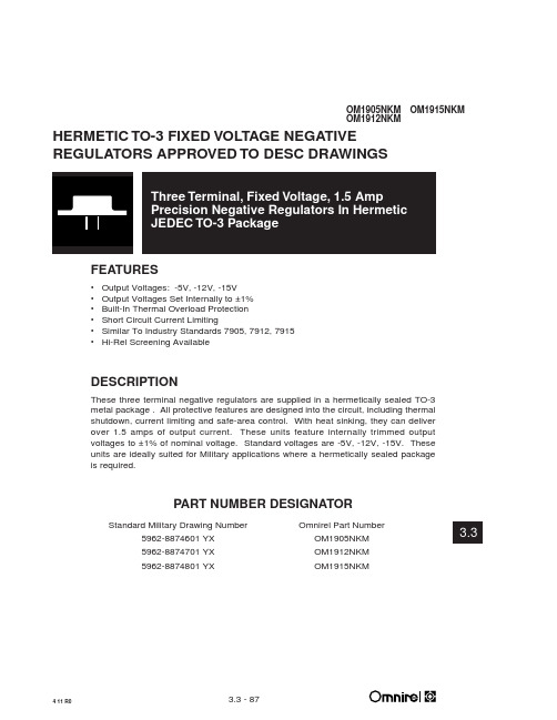
3.3HERMETIC TO-3 FIXED VOLTAGE NEGATIVEREGULATORS APPROVED TO DESC DRAWINGSFEATURES•Output Voltages: -5V, -12V, -15V•Output Voltages Set Internally to ±1%•Built-In Thermal Overload Protection•Short Circuit Current Limiting•Similar To Industry Standards 7905, 7912, 7915•Hi-Rel Screening AvailableDESCRIPTIONThese three terminal negative regulators are supplied in a hermetically sealed TO-3metal package . All protective features are designed into the circuit, including thermal shutdown, current limiting and safe-area control. With heat sinking, they can deliver over 1.5 amps of output current. These units feature internally trimmed output voltages to ±1% of nominal voltage. Standard voltages are -5V, -12V, -15V. These units are ideally suited for Military applications where a hermetically sealed package is required.PART NUMBER DESIGNATORStandard Military Drawing Number Omnirel Part Number5962-8874601 YX OM1905NKM5962-8874701 YX OM1912NKM5962-8874801 YX OM1915NKMOM1915NKM OM1905NKM OM1912NKMOM1905NKM - OM1915NKM3.3ELECTRICAL CHARACTERISTICS -5 Volt VIN= -10V, I o= 500mA, -55°C T A 125°C (unless otherwise specified) Parameter Symbol Test Conditions Min.Max.UnitOutput Voltage V OUT T A= 25°C-4.95-5.05VV IN= -7.5V to -20V•-4.85-5.15VI O = 5mA to 1.0 A, P<20WLine Regulation V RLINE V IN= -7.5V to -20V12mV (Note 1)•25mV(Note 4)V IN= -8.0V to -12V5mV•12mV Load Regulation V RLOAD I O = 5mA to 1.5 Amp20mV (Note 1)•25mVI O = 250mA to 750 mA15mV•30mV Standby Current Drain I SCD 2.5mA• 3.0mA Standby Current Drain D I SCD V IN= -7.0V to -20V•0.4mA Change With Line(Line)Standby Current Drain D I SCD I O= 5mA to 1000mA•0.4mA Change With Load(Load)Dropout Voltage V DO D V OUT= 100mV, I O=1.0A• 2.5V Peak Output Current I O (pk) T A= 25°C 1.5 3.3A Short Circuit Current I DS V IN= -35V 1.2A (Note 2)• 2.8A Ripple Rejection D V IN f =120 Hz, D V IN= -10V63dBD V OUT(Note 3)•60dBOutput Noise Voltage N O T A= 25°C, f =10 Hz to 100KHz40µV/V (Note 3)RMS Long Term Stability D V OUT T A= 25°C, t = 1000 hrs.75mV (Note 3)D tNotes:1.Load and Line Regulation are specified at a constant junction temperature. Pulse testing with low duty cycle is used.Changes in output voltage due to heating effects must be taken into account separately.2.Short Circuit protection is only assured up to V IN= -35V.3.If not tested, shall be guaranteed to the specified limits.The • denotes the specifications which apply over the full operating temperature range.ABSOLUTE MAXIMUM RATINGS @ 25°CInput Voltage. . . . . . . . . . . . . . . . . . . . . . . . . . . . . . . . . . . . . . . . . . . . . . . . . . . . . . . . . . -35 V Operating Junction Temperature Range . . . . . . . . . . . . . . . . . . . . . . . . . . .- 55°C to + 150°C Storage Temperature Range . . . . . . . . . . . . . . . . . . . . . . . . . . . . . . . . . . . . . . - 65°C to + 150°C Typical Power/Thermal Charateristics:Rated Power @ 25°C T C. . . . . . . . . . . . . . . . . . . . . . . . . . . . . . . . . . . . . . . . . . . . . . . 20WT A . . . . . . . . . . . . . . . . . . . . . . . . . . . . . . . . . . . . . . . . . . . . . . . 3.6W Thermal Resistance q JC . . . . .. . . . . . . . . . . . . . . . . . . . . . . . . . . . . . . . . . . . . 4.2°C/W aa q JA.. . . . . . . . . . . . . . . . . . . . . . . . . . . . . . . . . . . . . . . . . . . 42°C/WOM1905NKM - OM1915NKM3.3PLANE2 PLCS.Pin Connection Pin 1: Ground Pin 2: Output Case: InputOM1905NKM - OM1915NKM3.3。
590中文资料

1 出厂默认设置2 |__菜单3 | |__诊断4 | | |__[089] 速度给定SPEED DEMAND4 | | |__[297] 速度错误R SPEED ERROR4 | | |__[549] 速度回路输出SPD LOOP O/P 4 | | |__[299] 电流给定CURRENT DEMAND4 | | |__[298] 电流反馈CURRENT FEEDBACK 4 | | |__[538] 电流反馈AMPS CURRENT FBK.AMPS 4 | | |__[065] IaFbk,未过滤的IaFbk UNFILTERED 4 | | |__[066] IaDmd,未过滤的IaDmd UNFILTERED 4 | | |__[087] 正电流钳位POS. I CLAMP4 | | |__[088] 负电流钳位NEG. I CLAMP4 | | |__[067] 实际正电流钳位ACTUAL POS I LIM 4 | | |__[061]实际负电流钳位ACTUAL NEG I LIM) 4 | | |__[203] 所保留的反比时间O/P INVERSE TIME O/P 4 | | |__[042] 电流限值电流限值4 | | |__[077] 零速度AT ZERO SPEED4 | | |__[078] 零设定值AT ZREO SETPOINT 4 | | |__[079] 停止AT STANDSTILL4 | | |__[113] 斜坡RAMPING4 | | |__[080] 程序性停止PROGRAM STOP4 | | |__[525] 惯性停止COAST S至P4 | | |__[082] 调速器的启动DRIVE START4 | | |__[084] 启用调速器DRINE EVABLE4 | | |__[212] 运行模式OPERATING MODE4 | | |__[169] 已启用励磁FIELD ENABLED4 | | |__[183] 励磁给定FIELD DEMAND4 | | |__[300] 励磁电流反馈FIELD I FBK.4 | | |__[539] 励磁电流反馈AMPS FIELD I FBK.AMPS 4 | | |__[181] RAW励磁电流反馈RAW FIELD FBK4 | | |__[184] 励磁射角FLD.FIRING ANGLE 4 | | |__[050] ANIN 1 (A2)ANIN 1 (A2)4 | | |__[051] ANIN 2 (A3)ANIN 2 (A3)4 | | |__[052] ANIN 3 (A4)4 | | |__[053] ANIN 4 (A5)4 | | |__[055] ANOUT 1 (A7)4 | | |__[056] ANOUT 2 (A8)ANOUT 2 (A8)4 | | |__[068] 启动(C3)START (C3)4 | | |__[069] 数字输入端 C4DIGITAL INPUT C4 4 | | |__[070] 数字输入端 C5DIGITAL INPUT C5 4 | | |__[071] DIGIN 1 (C6)4 | | |__[072] DIGIN 2 (C7)4 | | |__[073] DIGIN 3 (C8)4 | | |__[074] DIGOUT 1 (B5)4 | | |__[075] DIGOUT 2 (B6)4 | | |__[076] DIGOUT 3 (B7)4 | | |__[264] 提高与降低O/P RAISE/LOWER O/P 4 | | |__[417] PID输出PID OUTPUT4 | | |__[416] PID钳位PID CLAMPED4 | | |__[415] PID错误PID ERROR4 | | |__[086] 速度求和数输出SPT SUM OUTPUT4 | | |__[085] 斜坡输出RAMP OUTPUT4 | | |__[063] 速度设定值4 | | |__[057] 端子电压TERMNAL VOLTS4 | | |__[060] 反电动势BACK EMT4 | | |__[308] 测速输入TACH INPUT4 | | |__[058] 未过滤的测速输入4 | | |__[206] 编码器ENCODER4 | | |__[059] 未过滤的编码器4 | | |__[062] 未过滤的速度反馈4 | | |__[064] 未过滤的速度错误4 | | |__[122] 正常指示灯HEALTH LED4 | | |__[125] 准备就绪READY4 | | |__[376] 运行中的调速器DRIVE RUNNING4 | | |__[374] 系统复位SYSTEM RESET3 | |__设置参数4 | | |__斜坡RAMPING5 | | | |__[002]斜坡加速时间RAMP ACCEL TIME)5 | | | |__[003] 斜坡减速时间RAMP DECEL TIME)5 | | | |__[004] 所保留的连续加速CONSTANT ACCEL) 5 | | | |__[118] 斜坡保持RAMP HOLD5 | | | |__[266] % S-斜坡% S-RAMP5 | | | |__[286] 斜线提高起点RAMPING THRESH.5 | | | |__[287] 自动复位AUTO RESET5 | | | |__[288] 外部复位EXTERNAL RESET 5 | | | |__[422] 复位值RESET VALUE5 | | | |__[126] 最小速度MIN SPEED4 | | |__辅助输入与输出5 | | | |__[161] 辅助启动AUX START5 | | | |__[227] 辅助点动AUX JOG5 | | | |__[168] 辅助启用AUX ENABLE5 | | | |__[094] 辅助DIGOUT 1辅助DIGOUT 15 | | | |__[095] 辅助DIGOUT 25 | | | |__[096] 辅助DIGOUT 35 | | | |__[128] ANOUT 15 | | | |__[129] ANOUT 25 | | | |__[496] 点动/慢动JOG/SLACK5 | | | |__[497] 启用ENABLE5 | | | |__[535] 启用REM.SEQ.5 | | | |__[536] REM.SEQUENCE5 | | | |__[537] SEQ状态4 | | |__操作站5 | | | |__设置6 | | | | |__[512] 设定值SETPOINT6 | | | | |__[513] 点动设定值JOG SETPOINT6 | | | | |__[511] 启用本地按键LOCAL KEY ENABLE5 | | | |__启动值6 | | | | |__[519] 设定值SETPOINT6 | | | | |__[520] 点动设定值JOG SETPOINT6 | | | | |__[516] 前向FORWARD6 | | | | |__[518] 程序PROGRAM6 | | | | |__[517] 本地LOCAL5 | | | |__本地斜坡6 | | | | |__[514] 斜坡加速时间RAMP ACCEL TIME 6 | | | | |__[515] 斜坡减速时间RAMP ACCEL TIME4 | | |__点动/慢动5 | | | |__[218] 点动速度1JOG SPEED 15 | | | |__[253] TAKE UP 15 | | | |__[254] TAKE UP 25 | | | |__[225] 微动速度CRAWL SPEED5 | | | |__[228] 模式MODE5 | | | |__[355] 斜坡率MIN VALUE4 | | |__提高与降低5 | | | |__[255] 复位值RESET VALUE5 | | | |__[256] 增加率INCREASE RATE 5 | | | |__[257] 降低率DECREASE RATE 5 | | | |__[261] 提高输入RAISE INPUT5 | | | |__[262] 降低输入LOWER INPUT5 | | | |__[258] 最小值MIN VALUE5 | | | |__[259] 最大值MAX VALUE5 | | | |__[307] 外部复位EXTERNAL RESET4 | | |__特殊功能块5 | | | |__直径运算6 | | | | |__[424]线速LINE SPEED6 | | | | |__[437] 卷轴旋转速度REEL SPEED6 | | | | |__[425] 最小速度MIN DIAMETER6 | | | | |__[426] 最小速度6 | | | | |__[462] 复位值RESET VALUE6 | | | | |__[463] 外部复位EXTERNAL RESET 6 | | | | |__[453] 斜坡率RAMP RATE6 | | | | |__[427] 直径DIAMETER6 | | | | |__[428] 线速模式MOD OF LINE SPD 6 | | | | |__[429] 卷轴旋转速度模式MOD OF REEL SPD 6 | | | | |__[430] 未过滤直径UNFILT DIAMETER5 | | | |__锥度运算.6 | | | | |__[438] 锥度TAPER6 | | | | |__[439] 张力支持TENSION SPT.6 | | | | |__[452] 渐变给定TAPERED DEMAND 6 | | | | |__[440] 张力调整TENSION TRIM6 | | | | |__[441] 全部.张力给定至T.TENS.DEMAND5 | | | |__转矩运算6 | | | | |__[432] 转矩给定至RQUE DEMAND 6 | | | | |__[433] 启用张力TENSION ENABLE5 | | | |__设定值和数26 | | | | |__[445] 输入 2INPUT 26 | | | | |__[443] 输入 1INPUT 16 | | | | |__[444] 输入 0INPUT 06 | | | | |__[446] 比率 1RATIO6 | | | | |__[447] 比率 0RATIO 06 | | | | |__[466] 除数 1DIVIDER 16 | | | | |__[448] 除数 0DIVIDER 06 | | | | |__[449] 限值LIMIT6 | | | | |__[451] 速度求和数输出SPT SUM OUTPUT6 | | | | |__[491] STPT 和数 2输出0STPT SUM 2 OUT 0 6 | | | | |__[492] STPT 和数 2输出STPT SUM 2 OUT 105 | | | |__PID6 | | | | |__[404] 比例增益PROP. GAIN6 | | | | |__[402] 速度积分时间INT.TIME.CONST6 | | | | |__[401] 微分 时间常数DERIVATIVE TC6 | | | | |__[405] 正限值POSITIVE LIMIT6 | | | | |__[406] 负限值NEGATIVE LIMIT6 | | | | |__[407] O/P计数器(调整)O/P SCALER(TRIM) 6 | | | |__[410] 输入 1INPUT 16 | | | | |__[411] 输入 2INPUT 26 | | | | |__[412] 比率 1RATIO 16 | | | | |__[413] 比率 2RATIO 26 | | | | |__[418] 除数 1DIVIDER 16 | | | | |__[414] 除数 2DIVIDER 26 | | | | |__[408] 启用ENABLE6 | | | | |__[409] INT. DEFEAT INT. DEFEAT6 | | | | |__[403] 滤波器T.C.FILTER T.C.6 | | | | |__[473] 模式MODE6 | | | | |__[474] 最小分布增益MIN PROFILE GAIN 6 | | | | |__[475] 分布式增益PROFILED GAIN5 | | | |__TENS+COMP运算3-PHASE FIELD6 | | | | |__[487]动态COMP STATIC COMP6 | | | | |__[489] 过卷REWIND6 | | | | |__[479] 固定惯量补偿FIX.INERTIA COMP 6 | | | | |__[480] 可变惯量补偿VAR.INERTIA COMP6 | | | | |__[498] 线速支持LINE SPEED SPT 6 | | | | |__[482] 滤波器T.C.FILTER T.C.6 | | | | |__[483] 比率运算RATE CAL6 | | | | |__[484] 标准化dv/dt NORMALISED dv/dt 6 | | | | |__[485] 惯量COMP O/P INERTIA COMP O/P 6 | | | | |__[486] 张力计数器TENSION SCALER4 | | |__励磁控制5 | | | |__[170] 启用励磁FIELD ENABLE5 | | | |__[209] 励磁控制模式FLD.CTRL MODE l5 | | | |__励磁电压变化6 | | | | |__[210] 励磁电压比FLD.VOLTS RATIO5 | | | |__励磁电流变化6 | | | | |__[171] 设定值SETPOINT6 | | | | |__[173] 比例.增益PROP. GAIN6 | | | | |__[172] 积分增益INT. GAIN6 | | | | |__弱磁变化7 | | | | | |__[174] 启用弱磁FLD. WEAK ENABLE 7 | | | | | |__[175] 电动势超前EMF LEAD7 | | | | | |__[176] 电动势滞后EMF LAG7 | | | | | |__[177] 电动势增益EMF GAIN7 | | | | | |__[179] 最小励磁电流MIN FLD.CURRENT 7 | | | | | |__[178] 最大电压MAX VOLTS7 | | | | | |__[191] 电动势反馈超前BEMF FBK LEAD7 | | | | | |__[192] 反电动势反滞后BEMF FBK LAG5 | | | |__[185] 弱磁延迟FLD.QUENCH DELAY 5 | | | |__[186] 弱磁模式FLD. QUENCH MODE4 | | |__电流分布5 | | | |__[032] 速度反馈1 (较低)5 | | | |__[031] 速度反馈2 (较高)5 | | | |__[093] 电流最大反馈1(SPD1)IMAX BRK1(SPD1) 5 | | | |__[033] 电流最大反馈2(SPD2)4 | | |__所保留的反比时间5 | | | |__[204] 所保留的目标AIMING POINT5 | | | |__[199] 所保留的“延迟”DELAY5 | | | |__[200] 所保留的“比率”RATE4 | | |__停止速度5 | | | |__[217] 停止限值STOP LIMIT5 | | | |__[302] 接触器延迟CONTACTOR DELAY 5 | | | |__[026] 程序性停止时间5 | | | |__[216] 程序性停止限值PROG STOP LIMIT 5 | | | |__[091] 程序性停止电流限值PROG STOP I LIM 5 | | | |__[029] 停止零速度4 | | |__校准5 | | | |__[039] 启用配置功能5 | | | |__[521] 额定电机电压NOM MO至R VOLTS 5 | | | |__[523] 电枢电流ARMATURE CURRENT 5 | | | |__[524] 励磁电流FIELD CURRENT5 | | | |__[020] 电枢电压运算.5 | | | |__[021] IR补偿5 | | | |__[022] 编码器RPM5 | | | |__[024] 编码器进线5 | | | |__[023] 模拟测速运算5 | | | |__[010] 零速度偏移5 | | | |__[025] 电枢 I (A9)5 | | | |__[180] 速度反馈报警级SPDFBK ALM LEVEL 5 | | | |__[263] 故障停止起点STALL THRESHOLD 5 | | | |__[224] 故障停止跳闸延迟STALL TRIP DELAY 5 | | | |__[541] REM跳闸延迟REM TRIP DELAY 5 | | | |__[188] 所保留的超速级OVER SPEED LEVEL 5 | | | |__[182] 励磁电流校准FIELD I CAL.4 | | |__禁用报警器5 | | | |__[019] 励磁故障5 | | | |__[111] 5703 接受错误5703 RCV ERROR 5 | | | |__[028] 故障停止跳闸5 | | | |__[305] 跳闸复位TRIP RESET5 | | | |__[081] 速度反馈报警5 | | | |__[092] 编码器报警ENCODER ALARM5 | | | |__[540] REM跳闸禁用REM TRIP INHIBIT4 | | |__电流回路5 | | | |__[421] 主电流限值MAIN CURR. LIMIT 5 | | | |__[016] 比例.增益5 | | | |__[017] 积分 增益5 | | | |__[136] 所保留的“前向馈入”FEED FORWARD5 | | | |__[137] 非连续性DISCONTINUOUS5 | | | |__[030] 辅助给定5 | | | |__[090] 双极电流钳位5 | | | |__[201] 反馈模式REGEN MODE5 | | | |__[527] 主电桥MASTER BRIDGE5 | | | |__[301] 正电流钳位POS. I CLAMP5 | | | |__[048] 负电流钳位5 | | | |__[119] 电流给定隔离I DMD. ISOLATE 5 | | | |__[015] 电流限值与计数器4 | | |__速度回路5 | | | |__[014] 速度比例.增益5 | | | |__[013] 速度.INT.TIME5 | | | |__[202] INT. DEFEAT INT. DEFEAT5 | | | |__[049] 编码器信号5 | | | |__[047] 速度反馈选择5 | | | |__[547] 速度反馈滤波器SPD.FBK.FILTER5 | | | |__高级6 | | | | |__适应性7 | | | | | |__[268] 模式MODE7 | | | | | |__[269] 速度反馈1 (较低)SPD BRK1 (LOW) 7 | | | | | |__[270] 速度反馈2 (较高)SPD BRK2 (HIGH) 7 | | | | | |__[271] 比例. 增益PROP. GAIN7 | | | | | |__[272] 速度.积分时间SPD.INT.TIME6 | | | | |__[274] 斜坡电流增益I GAIN IN RAMPPOS. LOOP P GAIN 6 | | | | |__[273] 所保留的正向回路P增6 | | | | |__零速度弱化7 | | | | | |__[284] 零速度级ZERO SPD. LEVEL 7 | | | | |__[285] 零IAD级ZERO IAD LEVEL5 | | | |__设定值6 | | | | |__[289] 设定值 1SETPOINT 16 | | | | |__[009] 信号 2 (A3)6 | | | | |__[007] 比率 2 (A3)6 | | | | |__[290] 设定值 2 (A3)SETPOINT 2 (A3) 6 | | | | |__[291] 设定值 3SETPOINT 36 | | | | |__[041] 设定值 46 | | | | |__[358] 最小给定MIN DEMAND4 | | |__停止5 | | | |__[011] 停止逻辑5 | | | |__[012] 零起点5 | | | |__[306] 所保留的源标记SOURCE TAG4 | | |__设定值和数15 | | | |__[006] 比率 15 | | | |__[208] 比率把 0RATIO 05 | | | |__[008] 信号 15 | | | |__[292] 信号 0SIGN 05 | | | |__[419] 除数 1DIVIDER 15 | | | |__[420] 除数 0DIVIDER 05 | | | |__[131] 静带宽度DEADBAND WIDTH 5 | | | |__[375] 限值LIMIT5 | | | |__[423] 输入 2INPUT 25 | | | |__[100] 输入 1INPUT 15 | | | |__[309] 输入 0INPUT 03 | |__密码4 | | |__[120] 输入密码ENTER PASSWORD 4 | | |__[526] 所保留的安全密码BY-PASS PASSWORD 4 | | |__[121] 修改密码CHANGE PASSWORD3 | |__报警状态4 | | |__[528] 最后的报警LAST ALARM4 | | |__[115] 正常字HEALTH WORD4 | | |__[116] 正常存储HEALTH STORE4 | | |__[337] 电机温度传感器状态THERMIS至R STATE 4 | | |__[472] 速度反馈状态SPEED FBK STATE 4 | | |__[112] 故障停止跳闸STALL TRIP4 | | |__[542] 远程跳闸REMOTE TRIP3 | |__菜单4 | | |__[037] 全部菜单4 | | |__语言5 | | | |__英语3 | |__[354] 参数保存PARAMETER SAVE3 | |__串行链路4 | | |__技术选项5 | | | |__[501] 技术选项输入1Te Option IN 1 5 | | | |__[502] 技术选项输入 2Te Option IN 2 5 | | | |__[503] 技术选项输入 3Te Option IN 3 5 | | | |__[504] 技术选项输入 4Te Option IN 4 5 | | | |__[505] 技术选项输入5Te Option IN 5 5 | | | |__[506] 技术选项故障Te Option FAULT 5 | | | |__[507] 技术选项修改Te Option VER 5 | | | |__[508] 技术选项输出 1Te Option OUT 1 5 | | | |__[509] 技术选项输出 2Te Option OUT24 | | |__系统端口(P3)5 | | | |__P3 设置6 | | | | |__[130] 模式MODE6 | | | | |__5703 支持7 | | | | | |__[132] 设置比率SETPT. RATIO7 | | | | | |__[133] SETPT.信号SETPT. SIGN7 | | | | | |__[187]原始输入RAW INPUT7 | | | | | |__[189] 测定输入SCALED INPUT6 | | | | |__双同步支持7 | | | | | |__[329] 群组ID (GID)GROUP ID (GID) 7 | | | | | |__[330] 个体ID (UID)UNIT ID (UID) 7 | | | | | |__[332] 错误报告ERROR REPORT6 | | | | |__[198] P3 波特率5 | | | |__DUMP MMI (TX)6 | | | | |__UP TO ACTION5 | | | |__UDP XFER (RX)6 | | | | |__UP TO ACTION5 | | | |__UDP XFER (TX)6 | | | | |__UP TO ACTION5 | | | |__[155] 版本号4 | | |__PNO配置5 | | | |__[312] PNO 112PNO 1125 | | | |__[313] PNO 113PNO 1135 | | | |__[314] PNO 114PNO 1145 | | | |__[315] PNO 115PNO 1155 | | | |__[316] PNO 116PNO 1165 | | | |__[317] PNO 117PNO 1175 | | | |__[319] PNO 119PNO 1195 | | | |__[320] PNO 120PNO 1205 | | | |__[321] PNO 121PNO 1215 | | | |__[322] PNO 122PNO 1225 | | | |__[323] PNO 123PNO 1235 | | | |__[324] PNO 124PNO 1245 | | | |__[325] PNO 125PNO 1255 | | | |__[326] PNO 126PNO 1265 | | | |__[327] PNO 127PNO 1273 | |__系统4 | | |__软件5 | | | |__ENGLISHNov 11 194 | | |__配置输入与输出5 | | | |__[039] 配置功能5 | | | |__模拟输入6 | | | | |__ANIN 1 (A2)7 | | | | | |__[230] 校准CALIBRATION7 | | | | | |__[231] 最大值MAX VALUE7 | | | | | |__[232] 最小值MIN VALUE7 | | | | | |__[246] 目的地标记DESTINATION TAG6 | | | | |__ANIN 2 (A3)7 | | | | | |__[233] 校准CALIBRATION7 | | | | | |__[234] 最大值MAX VALUE7 | | | | | |__[235] 最小值MIN VALUE7 | | | | | |__[493] 输出OUTPUT6 | | | | |__ANIN 3 (A4)7 | | | | | |__[236] 校准CALIBRATION7 | | | | | |__[237] 最大值MAX VALUE7 | | | | | |__[238] 最小值MIN VALUE7 | | | | | |__[249] 目的地标记DESTINATION TAG6 | | | | |__ANIN 4 (A5)7 | | | | | |__[239] 校准CALIBRATION7 | | | | | |__[240] 最大值MAX VALUE7 | | | | | |__[241] 最小值MIN VALUE7 | | | | | |__[250] 目的标记DESTINATION TAG6 | | | | |__ANIN 5 (A6)7 | | | | | |__[242] 校准CALIBRATION7 | | | | | |__[243] 最大值MAX VALUE7 | | | | | |__[244] 最小值MIN VALUE7 | | | | | |__[247] 目的标记DESTINATION TAG5 | | | |__模拟输出6 | | | | |__ANOUT 1 (A7)7 | | | | | |__[245] % TO GET 10V7 | | | | | |__[362] 系数MODULUS7 | | | | | |__[464] 偏移MODULUS7 | | | | | |__[251] 源标记SOURCE TAG6 | | | | |__ANOUT 2 (A8)7 | | | | | |__[248] % TO GET 10V TO GET 10V7 | | | | | |__[363] 系数MODULUS7 | | | | | |__[465] 偏移MODULUS7 | | | | | |__[252] 源标记SOURCE TAG5 | | | |__数字输入6 | | | | |__数字输入 C47 | | | | | |__[494] 目的标记DESTINATION TAG6 | | | | |__数字输入C57 | | | | | |__[495] 目的标记DESTINATION TAG6 | | | | |__DIGIN 1 (C6)7 | | | | | |__[103] 真值VALUE FOR TRUE 7 | | | | | |__[104]假值VALUE FOR FALSE 7 | | | | | |__[102] 目的标记DESTINATION TAG6 | | | | |__DIGIN 2 (C7)7 | | | | | |__[106] 真值VALUE FOR TRUE 7 | | | | | |__[107] 虚值VALUE FOR FALSE 7 | | | | | |__[105] 目的标记DESTINATION TAG6 | | | | |__DIGIN 3 (C8)7 | | | | | |__[109] 真值VALUE FOR TRUE 7 | | | | | |__[110] 假值VALUE FOR FALSE 7 | | | | | |__[108] 目的标记DESTINATION TAG5 | | | |__数字输出6 | | | | |__DIGOUT 1 (B5)7 | | | | | |__[195] 起点 (>)THRESHOLD (>) 7 | | | | | |__[043] 系数7 | | | | | |__[097] 源标记SOURCE7 | | | | | |__[359] 已转换INVERTED6 | | | | |__DIGOUT 2 (B6)7 | | | | | |__[196] 起点 (>)THRESHOLD (>)7 | | | | | |__[044] 系数7 | | | | | |__[098] 源标记SOURCE7 | | | | | |__[360] 已转换INVERTED6 | | | | |__DIGOUT 3 (B7)7 | | | | | |__[197] 起点 (>)THRESHOLD (>)7 | | | | | |__[045] 系数7 | | | | | |__[099] 源标记SOURCE7 | | | | | |__[361] 已转换INVERTED5 | | | |__配置57036 | | | | |__[134] 源标记SOURCE6 | | | | |__[135] 目的标记DESTINATION TAG5 | | | |__框图6 | | | | |__[260] 提高与降低DEST RAISE/LOWER DEST 6 | | | | |__[293] 斜坡 O/P DEST RAMP O/P DEST6 | | | | |__[294] 速度求和 1 目的地SPT SUM 1 DEST 6 | | | | |__[400] PID O/P DEST PID O/P DEST6 | | | | |__[431] 直径DIAMETER6 | | | | |__[442] 锥度TAPER6 | | | | |__[450] 设定值和数2SETPOINT SUM 2 6 | | | | |__[435] 正电流钳位POS. I CLAMP6 | | | | |__[436] 负电流钳位NEG. I CLAMP6 | | | | |__[478] 张力+补偿运算TENS+COMP CALC.5 | | | |__内部链路6 | | | | |__链路 17 | | | | | |__[364] 源标记7 | | | | | |__[365] 目的标记6 | | | | |__链路27 | | | | | |__[366] 源标记7 | | | | | |__[367] 目的标记6 | | | | |__链路 37 | | | | | |__[368] 源标记7 | | | | | |__[369] 目的标记6 | | | | |__链路 47 | | | | | |__[370] 源标记7 | | | | | |__[371] 目的标记6 | | | | |__链路 57 | | | | | |__[454] 源标记7 | | | | | |__[455] 目的标记6 | | | | |__链路 67 | | | | | |__[456] 源标记7 | | | | | |__[457] 目的标记6 | | | | |__链路 77 | | | | | |__[458] 源标记7 | | | | | |__[459] 目的标记6 | | | | |__链路 87 | | | | | |__[460] 源标记7 | | | | | |__[461] 目的标记6 | | | | |__链路 97 | | | | | |__[467] 源标记7 | | | | | |__[468] 目的标记6 | | | | |__链路 107 | | | | | |__[469] 源标记7 | | | | | |__[470] 目的标记6 | | | | |__链路 117 | | | | | |__[390] 源标记7 | | | | | |__[391] 目的标记7 | | | | | |__[392] 高级7 | | | | | |__[393] 模式7 | | | | | |__[394] 辅助源6 | | | | |__链路 127 | | | | | |__[395] 源标记7 | | | | | |__[396] 目的标记7 | | | | | |__[397] 高级7 | | | | | |__[398] 模式7 | | | | | |__[399] 辅助源4 | | |__保留的“保留”功能5 | | | |__仅工厂使用6 | | | | |__禁止修改 !!7 | | | | | |__[162] 所保留的“MIN MM MIN MMI CYCLE TM 7 | | | | | |__[163] 所保留的“ ILOOP PI MODE”7 | | | | | |__[164] 所保留的“TOGGLE PERIOD”7 | | | | | |__[165] 所保留的“TOGGLE REF 1”7 | | | | | |__[166] 所保留的“SEL. INT/CUR/SPD”7 | | | | | |__[167] 所保留的“TOGGLE REF 2”7 | | | | | |__[190] 所保留的“PEAK HW SLOPE”7 | | | | | |__[226] 所保留的“PEAK HW OFFSET”7 | | | | | |__[211] 所保留的“HEALTH INHIBIT”7 | | | | | |__[194] 所保留的“DISC ADAPT POT“7 | | | | | |__[193] 所保留的“TICK LENGTH”7 | | | | | |__[310] 所保留的“AUTOCAL“7 | | | | | |__[311] 所保留的“IAINST OFFSET”7 | | | | | |__[213] 所保留的“ZERO CUR OFFSET“7 | | | | | |__[214] 所保留的“ZCD THRESHOLD”7 | | | | | |__[221] 所保留的“MMI FILTER T.C.“7 | | | | | |__[222] 所保留的“PRED STEP”7 | | | | | |__[223] 所保留的“SCAN THRESHOLD“7 | | | | | |__[034] 所保留的“FIELD FBKSTOP”7 | | | | | |__[035] 所保留的“FIELD FFRSTOP“7 | | | | | |__[036] 所保留的“IFFB DELAY”7 | | | | | |__[154] 所保留的“II”7 | | | | | |__[101] 所保留的“MIN BS DEAD TIME”7 | | | | | |__[553] 所保留的“MAX BS DEAD TIME”7 | | | | | |__[276] 所保留的“PLL PROP”7 | | | | | |__[277] 所保留的“PLL INT”7 | | | | | |__[386] 所保留的“FILTER T.C.”7 | | | | | |__[279] 所保留的“ARM ENDSTOP”7 | | | | | |__[283] 所保留的“SCAN TC”7 | | | | | |__[280] 所保留的“HF C/O DISC GAIN”7 | | | | | |__[281] 所保留的“HF C/O FILTER TC”7 | | | | | |__[282] 所保留的“BEMF THRESHOLD”7 | | | | | |__[265] 所保留的“ANALOG IP OFFSET”7 | | | | | |__[388] 所保留的“SYNC OFFSET”7 | | | | | |__[205] 所保留的“dI/dt”7 | | | | | |__[335] 所保留的“DISABLE MEAN FBK”7 | | | | | |__[336] 所保留的“CHANGEOVER BIAS”7 | | | | | |__[471] 所保留的“STANDBY FIELD”7 | | | | | |__[476] 所保留的“3-PHASE FIELD”7 | | | | | |__[550] 所保留的“ENABLE 12 PULSE”7 | | | | | |__[551] 所保留的“MASTER BRIDGE”7 | | | | | |__[552] 所保留的“SLAVE BRIDGE”7 | | | | | |__[522] 所保留的“NOT 570 STACK”7 | | | | | |__[158] 所保留的“OP STATION ERROR”7 | | | | | |__[040] 所保留的“SYSTEM IO”7 | | | | | |__[046] 所保留的“ILOOP SUSPEND”7 | | | | | |__[114] 所保留的“SEQ STATE”7 | | | | | |__[117] 所保留的“HEALTH INHIBIT”7 | | | | | |__[215] 所保留的“G&L POWER METER”7 | | | | | |__[267] 所保留的“POSITION COUNT”7 | | | | | |__[275] 所保留的“POSITION DIVIDER”7 | | | | | |__[387] 所保留的“RAW POS COUNT”7 | | | | | |__[278] 所保留的“PLL ERROR”7 | | | | | |__[295] 所保留的“FILTER INPUT”7 | | | | | |__[296] 所保留的“FILTER OUTPUT”7 | | | | | |__[372] 所保留的“R/L DELTA”7 | | | | | |__[373] 所保留的“SYS RAMP DELTA”7 | | | | | |__[389] 所保留的“PERCENT RPM”7 | | | | | |__[529] 所保留的“PNO 39”7 | | | | | |__[530] 所保留的“PNO 47”7 | | | | | |__[531] 所保留的“PNO 55”7 | | | | | |__[532] 所保留的“PNO 63”7 | | | | | |__[533] 所保留的“PNO 71”7 | | | | | |__[534] 所保留的“PNO 95”4 | | |__浏览5 | | | |__[123] 浏览数据PEEK DATA5 | | | |__[124] 浏览范围PEEK SCALE4 | | |__最小化连接5 | | | |__[339] 数值 15 | | | |__[340] 数值 25 | | | |__[341] 数值 35 | | | |__[342] 数值 45 | | | |__[343] 数值 55 | | | |__[344] 数值 65 | | | |__[345] 数值 75 | | | |__[379] 数值 85 | | | |__[380] 数值 95 | | | |__[381] 数值 105 | | | |__[382] 数值 115 | | | |__[383] 数值 125 | | | |__[384] 数值 135 | | | |__[385] 数值 145 | | | |__[346] 逻辑 15 | | | |__[347] 逻辑 25 | | | |__[349] 逻辑 45 | | | |__[350] 逻辑 55 | | | |__[351] 逻辑 65 | | | |__[352] 逻辑 75 | | | |__[353] 逻辑 83 | |__配置调速器4 | | |__[039] 配置功能Configure Enable)4 | | |__[521] 额定电机电压NOM MO至R VOLTS4 | | |__[523] 电枢电流ARMATURE CURRENT 4 | | |__[524] 励磁电流FIELD CURRENT4 | | |__[543] 所保留的零校准输入ZERO CAL INPUTS4 | | |__[209] 励磁控制模式FLD.CTRL MODE l4 | | |__[210] 励磁电压比率FLD.VOLTS RATIO4 | | |__[018] 自动调整AUTOTUNE4 | | |__[047] 速度反馈选择SPEED FBK SELECT) 4 | | |__[024] 编码器进线ENCODER LINES)4 | | |__[022] 编码器RPM ENCODER RPM)4 | | |__[049] 编码器符号ENCODER SIGN)4 | | |__[013]速度积分时间SPD. INT TIME)4 | | |__[014] 速度比例增益SPD. PROP. GAIN)。
5962-9232501MXA资料
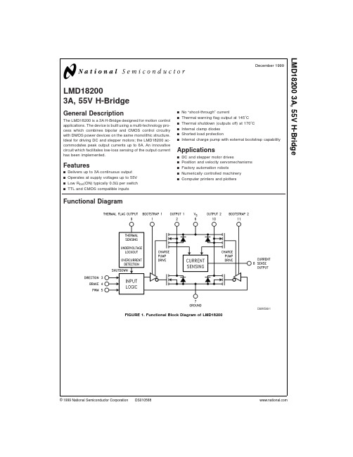
LMD182003A,55V H-BridgeGeneral DescriptionThe LMD18200is a 3A H-Bridge designed for motion control applications.The device is built using a multi-technology pro-cess which combines bipolar and CMOS control circuitry with DMOS power devices on the same monolithic structure.Ideal for driving DC and stepper motors;the LMD18200ac-commodates peak output currents up to 6A.An innovative circuit which facilitates low-loss sensing of the output current has been implemented.Featuresn Delivers up to 3A continuous output n Operates at supply voltages up to 55V n Low R DS (ON)typically 0.3Ωper switch nTTL and CMOS compatible inputsn No “shoot-through”currentn Thermal warning flag output at 145˚C n Thermal shutdown (outputs off)at 170˚C n Internal clamp diodes n Shorted load protectionnInternal charge pump with external bootstrap capabilityApplicationsn DC and stepper motor drivesn Position and velocity servomechanisms n Factory automation robotsn Numerically controlled machinery nComputer printers and plottersFunctional DiagramDS010568-1FIGURE 1.Functional Block Diagram of LMD18200December 1999LMD182003A,55V H-Bridge©1999National Semiconductor Corporation Connection Diagrams and Ordering InformationDS010568-211-Lead TO-220PackageTop ViewOrder Number LMD18200T See NS Package TA11BDS010568-2524-Lead Dual-in-Line PackageTop ViewOrder Number LMD18200-2D-QV5962-9232501VXA LMD18200-2D/8835962-9232501MXA See NS Package DA24BL M D 18200 2Absolute Maximum Ratings(Note1)If Military/Aerospace specified devices are required, please contact the National Semiconductor Sales Office/ Distributors for availability and specifications.Total Supply Voltage(V S,Pin6)60V Voltage at Pins3,4,5,8and912V Voltage at Bootstrap Pins(Pins1and11)V OUT+16V Peak Output Current(200ms)6A Continuous Output Current(Note2)3A Power Dissipation(Note3)25W Power Dissipation(T A=25˚C,Free Air)3W Junction Temperature,T J(max)150˚C ESD Susceptibility(Note4)1500V Storage Temperature,T STG−40˚C to+150˚C Lead Temperature(Soldering,10sec.)300˚COperating Ratings(Note1)Junction Temperature,T J−40˚C to+125˚C V S Supply Voltage+12V to+55VElectrical Characteristics(Note5)The following specifications apply for V S=42V,unless otherwise specified.Boldface limits apply over the entire operating temperature range,−40˚C≤T J≤+125˚C,all other limits are for T A=T J=25˚C.Symbol Parameter Conditions Typ Limit UnitsR DS(ON)Switch ON Resistance Output Current=3A(Note6)0.330.4/0.6Ω(max)R DS(ON)Switch ON Resistance Output Current=6A(Note6)0.330.4/0.6Ω(max)V CLAMP Clamp Diode Forward Drop Clamp Current=3A(Note6) 1.2 1.5V(max)V IL Logic Low Input Voltage Pins3,4,5−0.1V(min)0.8V(max)I IL Logic Low Input Current V IN=−0.1V,Pins=3,4,5−10µA(max)V IH Logic High Input Voltage Pins3,4,52V(min)12V(max)I IH Logic High Input Current V IN=12V,Pins=3,4,510µA(max)Current Sense Output I OUT=1A(Note8)377325/300µA(min)425/450µA(max) Current Sense Linearity1A≤I OUT≤3A(Note7)±6±9%Undervoltage Lockout Outputs turn OFF9V(min)11V(max)T JW Warning Flag Temperature Pin9≤0.8V,I L=2mA145˚CV F(ON)Flag Output Saturation Voltage T J=T JW,I L=2mA0.15VI F(OFF)Flag Output Leakage V F=12V0.210µA(max)T JSD Shutdown Temperature Outputs Turn OFF170˚CI S Quiescent Supply Current All Logic Inputs Low1325mA(max)t Don Output Turn-On Delay Time Sourcing Outputs,I OUT=3A300nsSinking Outputs,I OUT=3A300nst on Output Turn-On Switching Time Bootstrap Capacitor=10nFSourcing Outputs,I OUT=3A100nsSinking Outputs,I OUT=3A80nst Doff Output Turn-Off Delay Times Sourcing Outputs,I OUT=3A200nsSinking Outputs,I OUT=3A200nst off Output Turn-Off Switching Times Bootstrap Capacitor=10nFSourcing Outputs,I OUT=3A75nsSinking Outputs,I OUT=3A70nst pw Minimum Input Pulse Width Pins3,4and51µst cpr Charge Pump Rise Time No Bootstrap Capacitor20µsLMD182003Electrical Characteristics NotesNote 1:Absolute Maximum Ratings indicate limits beyond which damage to the device may occur.DC and AC electrical specifications do not apply when op-erating the device beyond its rated operating conditions.Note 2:See Application Information for details regarding current limiting.Note 3:The maximum power dissipation must be derated at elevated temperatures and is a function of T J(max),θJA ,and T A .The maximum allowable power dis-sipation at any temperature is P D(max)=(T J(max)−T A )/θJA ,or the number given in the Absolute Ratings,whichever is lower.The typical thermal resistance from junc-tion to case (θJC )is 1.0˚C/W and from junction to ambient (θJA )is 30˚C/W.For guaranteed operation T J(max)=125˚C.Note 4:Human-body model,100pF discharged through a 1.5k Ωresistor.Except Bootstrap pins (pins 1and 11)which are protected to 1000V of ESD.Note 5:All limits are 100%production tested at 25˚C.Temperature extreme limits are guaranteed via correlation using accepted SQC (Statistical Quality Control)methods.All limits are used to calculate AOQL,(Average Outgoing Quality Level).Note 6:Output currents are pulsed (t W <2ms,Duty Cycle <5%).Note 7:Regulation is calculated relative to the current sense output value with a 1A load.Note 8:Selections for tighter tolerance are available.Contact factory.Typical Performance CharacteristicsV SAT vs Flag CurrentDS010568-16R DS (ON)vs TemperatureDS010568-17R DS (ON)vs Supply VoltageDS010568-18Supply Current vs Supply VoltageDS010568-19Supply Current vs Frequency (V S =42V)DS010568-20Supply Current vsTemperature (V S =42V)DS010568-21Current Sense Output vs Load Current DS010568-22Current Sense Operating RegionDS010568-23L M D 18200 4Test CircuitSwitching Time DefinitionsPinout Description(See Connection Diagram) Pin1,BOOTSTRAP1Input:Bootstrap capacitor pin for half H-bridge number1.The recommended capacitor(10nF)is connected between pins1and2.Pin2,OUTPUT1:Half H-bridge number1output.Pin3,DIRECTION Input:See Table1.This input controls the direction of current flow between OUTPUT1and OUT-PUT2(pins2and10)and,therefore,the direction of rotation of a motor load.Pin4,BRAKE Input:See Table1.This input is used to brake a motor by effectively shorting its terminals.When braking is desired,this input is taken to a logic high level andit is also necessary to apply logic high to PWM input,pin5.The drivers that short the motor are determined by the logiclevel at the DIRECTION input(Pin3):with Pin3logic high,both current sourcing output transistors are ON;with Pin3logic low,both current sinking output transistors are ON.Alloutput transistors can be turned OFF by applying a logic highto Pin4and a logic low to PWM input Pin5;in this case onlya small bias current(approximately−1.5mA)exists at eachoutput pin.Pin5,PWM Input:See Table1.How this input(and DIREC-TION input,Pin3)is used is determined by the format of thePWM Signal.DS010568-8DS010568-9LMD182005Pinout Description(See Connection Diagram)(Continued)Pin 6,V S Power SupplyPin 7,GROUND Connection:This pin is the ground return,and is internally connected to the mounting tab.Pin 8,CURRENT SENSE Output:This pin provides the sourcing current sensing output signal,which is typically 377µA/A.Pin 9,THERMAL FLAG Output:This pin provides the ther-mal warning flag output signal.Pin 9becomes active-low at 145˚C (junction temperature).However the chip will not shut itself down until 170˚C is reached at the junction.Pin 10,OUTPUT 2:Half H-bridge number 2output.Pin 11,BOOTSTRAP 2Input:Bootstrap capacitor pin for Half H-bridge number 2.The recommended capacitor (10nF)is connected between pins 10and 11.TABLE 1.Logic Truth TablePWM Dir Brake Active Output Drivers H H L Source 1,Sink 2H L L Sink 1,Source 2L X L Source 1,Source 2H H H Source 1,Source 2H L H Sink 1,Sink 2LXHNONEApplication InformationTYPES OF PWM SIGNALSThe LMD18200readily interfaces with different forms of PWM e of the part with two of the more popular forms of PWM is described in the following paragraphs.Simple,locked anti-phase PWM consists of a single,vari-able duty-cycle signal in which is encoded both direction and amplitude information (see Figure 2).A 50%duty-cycle PWM signal represents zero drive,since the net value of voltage (integrated over one period)delivered to the load is zero.For the LMD18200,the PWM signal drives the direc-tion input (pin 3)and the PWM input (pin 5)is tied to logic high.Sign/magnitude PWM consists of separate direction (sign)and amplitude (magnitude)signals (see Figure 3).The (ab-solute)magnitude signal is duty-cycle modulated,and the absence of a pulse signal (a continuous logic low level)rep-resents zero drive.Current delivered to the load is propor-tional to pulse width.For the LMD18200,the DIRECTION in-put (pin 3)is driven by the sign signal and the PWM input (pin 5)is driven by the magnitude signal.SIGNAL TRANSITION REQUIREMENTSTo ensure proper internal logic performance,it is good prac-tice to avoid aligning the falling and rising edges of input sig-nals.A delay of at least 1µsec should be incorporated be-tween transitions of the Direction,Brake,and/or PWM input signals.A conservative approach is be sure there is at least 500ns delay between the end of the first transition and the beginning of the second transition.See Figure 4.DS010568-4FIGURE 2.Locked Anti-Phase PWM Control DS010568-5FIGURE 3.Sign/Magnitude PWM ControlL M D 18200 6Application Information(Continued)USING THE CURRENT SENSE OUTPUTThe CURRENT SENSE output(pin8)has a sensitivity of 377µA per ampere of output current.For optimal accuracy and linearity of this signal,the value of voltage generating re-sistor between pin8and ground should be chosen to limit the maximum voltage developed at pin8to5V,or less.The maximum voltage compliance is12V.It should be noted that the recirculating currents(free wheel-ing currents)are ignored by the current sense circuitry. Therefore,only the currents in the upper sourcing outputs are sensed.USING THE THERMAL WARNING FLAGThe THERMAL FLAG output(pin9)is an open collector tran-sistor.This permits a wired OR connection of thermal warn-ing flag outputs from multiple LMD18200’s,and allows the user to set the logic high level of the output signal swing to match system requirements.This output typically drives the interrupt input of a system controller.The interrupt service routine would then be designed to take appropriate steps, such as reducing load currents or initiating an orderly system shutdown.The maximum voltage compliance on the flag pin is12V.SUPPLY BYPASSINGDuring switching transitions the levels of fast current changes experienced may cause troublesome voltage tran-sients across system stray inductance.It is normally necessary to bypass the supply rail with a high quality capacitor(s)connected as close as possible to the V S Power Supply(Pin6)and GROUND(Pin7).A1µF high-frequency ceramic capacitor is recommended.Care should be taken to limit the transients on the supply pin be-low the Absolute Maximum Rating of the device.When oper-ating the chip at supply voltages above40V a voltage sup-pressor(transorb)such as P6KE62A is recommended from supply to ground.Typically the ceramic capacitor can be eliminated in the presence of the voltage suppressor.Note that when driving high load currents a greater amount of sup-ply bypass capacitance(in general at least100µF per Ampof load current)is required to absorb the recirculating cur-rents of the inductive loads.CURRENT LIMITINGCurrent limiting protection circuitry has been incorporatedinto the design of the LMD18200.With any power device it isimportant to consider the effects of the substantial surge cur-rents through the device that may occur as a result ofshorted loads.The protection circuitry monitors this increasein current(the threshold is set to approximately10Amps)and shuts off the power device as quickly as possible in theevent of an overload condition.In a typical motor driving ap-plication the most common overload faults are caused byshorted motor windings and locked rotors.Under these con-ditions the inductance of the motor(as well as any series in-ductance in the V CC supply line)serves to reduce the mag-nitude of a current surge to a safe level for the LMD18200.Once the device is shut down,the control circuitry will peri-odically try to turn the power device back on.This feature al-lows the immediate return to normal operation in the eventthat the fault condition has been removed.While the fault re-mains however,the device will cycle in and out of thermalshutdown.This can create voltage transients on the V CCsupply line and therefore proper supply bypassing tech-niques are required.The most severe condition for any power device is a direct,hard-wired(“screwdriver”)long term short from an output toground.This condition can generate a surge of currentthrough the power device on the order of15Amps and re-quire the die and package to dissipate up to500Watts ofpower for the short time required for the protection circuitryto shut off the power device.This energy can be destructive,particularly at higher operating voltages(>30V)so some precautions are in order.Proper heat sink design is essentialand it is normally necessary to heat sink the V CC supply pin(pin6)with1square inch of copper on the PCB.DS010568-24FIGURE4.Transitions in Brake,Direction,or PWM Must Be Separated By At Least1µsecLMD182007Application Information(Continued)INTERNAL CHARGE PUMP AND USE OF BOOTSTRAP CAPACITORSTo turn on the high-side (sourcing)DMOS power devices,the gate of each device must be driven approximately 8V more positive than the supply voltage.To achieve this an in-ternal charge pump is used to provide the gate drive voltage.As shown in Figure 5,an internal capacitor is alternately switched to ground and charged to about 14V,then switched to V supply thereby providing a gate drive voltage greater than V supply.This switching action is controlled by a con-tinuously running internal 300kHz oscillator.The rise time of this drive voltage is typically 20µs which is suitable for oper-ating frequencies up to 1kHz.For higher switching frequencies,the LMD18200provides for the use of external bootstrap capacitors.The bootstrap principle is in essence a second charge pump whereby a large value capacitor is used which has enough energy to quickly charge the parasitic gate input capacitance of the power device resulting in much faster rise times.The switch-ing action is accomplished by the power switches them-selves Figure 6.External 10nF capacitors,connected from the outputs to the bootstrap pins of each high-side switch provide typically less than 100ns rise times allowing switch-ing frequencies up to 500kHz.INTERNAL PROTECTION DIODESA major consideration when switching current through induc-tive loads is protection of the switching power devices from the large voltage transients that occur.Each of the four switches in the LMD18200have a built-in protection diode to clamp transient voltages exceeding the positive supply or ground to a safe diode voltage drop across the switch.The reverse recovery characteristics of these diodes,once the transient has subsided,is important.These diodes must come out of conduction quickly and the power switches must be able to conduct the additional reverse recovery current of the diodes.The reverse recovery time of the diodes protect-ing the sourcing power devices is typically only 70ns with a reverse recovery current of 1A when tested with a full 6A of forward current through the diode.For the sinking devices the recovery time is typically 100ns with 4A of reverse cur-rent under the same conditions.Typical ApplicationsFIXED OFF-TIME CONTROLThis circuit controls the current through the motor by apply-ing an average voltage equal to zero to the motor terminals for a fixed period of time,whenever the current through the motor exceeds the commanded current.This action causesthe motor current to vary slightly about an externally con-trolled average level.The duration of the Off-period is ad-justed by the resistor and capacitor combination of the LM555.In this circuit the Sign/Magnitude mode of operation is implemented (see Types of PWM Signals).DS010568-6FIGURE 5.Internal Charge Pump CircuitryDS010568-7FIGURE 6.Bootstrap CircuitryL M D 18200 8Typical Applications(Continued)TORQUE REGULATIONLocked Anti-Phase Control of a brushed DC motor.Current sense output of the LMD18200provides load sensing.The LM3525A is a general purpose PWM controller.The relationship of peak motor current to adjustment voltage is shown in Figure 10.DS010568-10FIGURE 7.Fixed Off-Time ControlDS010568-11FIGURE 8.Switching WaveformsLMD182009Typical Applications(Continued)VELOCITY REGULATIONUtilizes tachometer output from the motor to sense motor speed for a locked anti-phase control loop.The relationship of motor speed to the speed adjustment control voltage is shown in Figure 12.DS010568-12FIGURE 9.Locked Anti-Phase Control Regulates TorqueDS010568-13FIGURE 10.Peak Motor Currentvs Adjustment VoltageL M D 18200 10Typical Applications(Continued)DS010568-14FIGURE 11.Regulate Velocity with Tachometer FeedbackDS010568-15FIGURE 12.Motor Speed vsControl VoltageLMD1820011Physical Dimensionsinches (millimeters)unless otherwise noted11-Lead TO-220Power Package (T)Order Number LMD18200T NS Package Number TA11BL M D 18200 12Physical Dimensions inches(millimeters)unless otherwise noted(Continued)LIFE SUPPORT POLICYNATIONAL’S PRODUCTS ARE NOT AUTHORIZED FOR USE AS CRITICAL COMPONENTS IN LIFE SUPPORT DEVICES OR SYSTEMS WITHOUT THE EXPRESS WRITTEN APPROVAL OF THE PRESIDENT AND GENERAL COUNSEL OF NATIONAL SEMICONDUCTOR CORPORATION.As used herein:1.Life support devices or systems are devices orsystems which,(a)are intended for surgical implantinto the body,or(b)support or sustain life,andwhose failure to perform when properly used inaccordance with instructions for use provided in thelabeling,can be reasonably expected to result in asignificant injury to the user.2.A critical component is any component of a lifesupport device or system whose failure to performcan be reasonably expected to cause the failure ofthe life support device or system,or to affect itssafety or effectiveness.National SemiconductorCorporationAmericasTel:1-800-272-9959Fax:1-800-737-7018Email:support@National SemiconductorEuropeFax:+49(0)180-5308586Email:europe.support@Deutsch Tel:+49(0)180-5308585English Tel:+49(0)180-5327832Français Tel:+49(0)180-5329358Italiano Tel:+49(0)180-5341680National SemiconductorAsia Pacific CustomerResponse GroupTel:65-2544466Fax:65-2504466Email:sea.support@National SemiconductorJapan Ltd.Tel:81-3-5639-7560Fax:81-3-5639-7507 24-Lead Dual-in-Line PackageOrder Number LMD18200-2D-QV5962-9232501VXALMD18200-2D/8835962-9232501MXANS Package Number DA24BLMD182003A,55VH-Bridge National does not assume any responsibility for use of any circuitry described,no circuit patent licenses are implied and National reserves the right at any time without notice to change said circuitry and specifications.。
派克核电门户网站产品说明书

10 CFR 50 • AERB • ASME QME-1* • ASME QSC (NCA-3800) • ASME 第 III 部分 • ASME U核级认证核级认证 • ASN • CNSC CRN-N* HAF 604 • IAEA SC-QA 780 298* • IEEE* • ISO 9001: •E 派克核电门户网站无论您是要建新的发电厂,还是要改进现有电厂,派克都会依照行业统一的质量保证计划,使不同部门的各种产品进入核电市场,提高生产率和利润率。
这些产品包括安全专项和安全相关的核级子系统和组件,以及为非管制工厂区提供的优质的“成熟”商品。
派克门户网站是我们投入数百万美元用于核能研究和发展的承诺之一,是我们承诺提获得越来越多在全球供应且通过认证的核能产品的单一途径。
供行业所要求的高效性、可靠性和成本效益的体现。
我们支持单源购买各种产品系列,通过最新的订购方式提高工厂生产率和利润率。
另外,我们在将近 50 个国家拥有 50,000 名员工,因而门户网站产品在全球都有供应。
有关订购门户网站产品的更多信息,请:拨打电话 256 885 3833(销售)、256 885 3880(技术支持)或 发送电子邮件至 ipdusnuclear@parker .com派克核电门户网站是根据派克现行的 NQA- 1 和 10CFR50 附录 B 规定的质量保证计划开发的,并且采用了行业及规范性文件中规定的最佳实3 级阀门的 ASME N 核级认证外,派克核电门户网站上提供的产品符合 10CFR 第 21 部分中对基本组件的规定,按照认可的质保计划或是商品级物项执行。
专项不会提高质量,而是验证并记录专用项目中已有的的质量。
EU PED*HAF 604*IAEA SC-QA KTA 3507NNSANQA-1Parker Hannifin Ltd.Tachbrook Park DriveTachbrook Park,Warwick, CV34 6TU英国电话:+44 (0) 1926 317 878传真:+44 (0) 1926 317 855********************欧洲、中东和非洲AE – 阿联酋,迪拜电话:+971 4 8127100********************AT – 奥地利,维也纳新城电话:+43 (0)2622 23501-0*************************AT – 东欧,维也纳新城电话:+43 (0)2622 23501 900****************************AZ – 阿塞拜疆,巴库电话:+994 50 2233 458****************************BE/LU – 比利时,尼韦尔电话:+32 (0)67 280 900*************************BY – 白俄罗斯,明斯克电话:+375 17 209 9399*************************CH – 瑞士,埃托瓦电话:+41 (0)21 821 87 00*****************************CZ – 捷克共和国,Klecany电话:+420 284 083 111*******************************DE – 德国,卡尔斯特电话:+49 (0)2131 4016 0*************************DK – 丹麦,巴勒鲁普电话:+45 43 56 04 00*************************ES – 西班牙,马德里电话:+34 902 330 001***********************FI – 芬兰,万塔河电话:+358 (0)20 753 2500parker. ****************FR – 法国,Contamine s/Arve电话:+33 (0)4 50 25 80 25************************GR – 希腊,雅典电话:+30 210 933 6450************************HU – 匈牙利,布达佩斯电话:+36 23 885 470*************************IE – 爱尔兰,都柏林电话:+353 (0)1 466 6370*************************IT – 意大利,Corsico (MI)电话:+39 02 45 19 21***********************KZ – 哈萨克斯坦,阿拉木图电话:+7 7273 561 000****************************NL – 荷兰,奥尔登扎尔电话:+31 (0)541 585 000********************NO – 挪威,阿斯克尔电话:+47 66 75 34 00************************PL – 波兰,华沙电话:+48 (0)22 573 24 00************************PT – 葡萄牙,莱萨·达·帕尔梅拉电话:351 22 999 7360**************************RO – 罗马尼亚,布加勒斯特电话:+40 21 252 1382*************************RU – 俄罗斯,莫斯科电话:+7 495 645-2156************************SE – 瑞典,Spånga电话:+46 (0)8 59 79 50 00************************SK – 斯洛伐克,班斯卡·比斯特里察电话:+421 484 162 252**************************SL – 斯洛文尼亚,新梅斯托电话:+386 7 337 6650**************************TR – 土耳其,伊斯坦布尔电话:+90 216 4997081************************UA – 乌克兰,基辅电话:+380 44 494 2731*************************UK – 英国,沃里克电话:+44 (0)1926 317 878********************ZA – 南非,坎普顿公园电话:+27 (0)11 961 0700*****************************北美地区CA – 加拿大,安大略省米尔顿电话:+1 905 693 3000US – 美国,克利夫兰电话:+1 216 896 3000亚太地区AU – 澳大利亚,城堡山电话:+61 (0)2-9634 7777CN – 中国,上海电话:+86 21 2899 5000HK – 香港电话:+852 2428 8008IN – 印度,孟买电话:+91 22 6513 7081-85JP – 日本,东京电话:+81 (0)3 6408 3901KR – 韩国,首尔电话:+82 2 559 0400MY – 马来西亚,莎阿南电话:+60 3 7849 0800NZ – 新西兰,惠灵顿电话:+64 9 574 1744SG – 新加坡电话:+65 6887 6300TH – 泰国,曼谷电话:+662 186 7000-99TW – 台湾,台北电话:+886 2 2298 8987南美AR – 阿根廷,布宜诺斯艾利斯电话:+54 3327 44 4129BR – 巴西,圣若泽杜斯坎普电话:+55 800 727 5374CL – 智利,圣地亚哥电话:+56 2 623 1216MX – 墨西哥,阿波达卡电话:+52 81 8156 6000核电门户网站手册 M&K 12/10 1M派克授权的本地经销商© 2010 派克汉尼汾公司派克全球办事处联系信息欧洲产品信息中心免费电话:00 800 27 27 5374(AT, BE, CH, CZ, DE, DK, EE, ES, FI, FR, IE,IL, IS, IT, LU, MT, NL, NO, PL, PT, RU, SE,SK, UK, ZA)– 一点的方式。
- 1、下载文档前请自行甄别文档内容的完整性,平台不提供额外的编辑、内容补充、找答案等附加服务。
- 2、"仅部分预览"的文档,不可在线预览部分如存在完整性等问题,可反馈申请退款(可完整预览的文档不适用该条件!)。
- 3、如文档侵犯您的权益,请联系客服反馈,我们会尽快为您处理(人工客服工作时间:9:00-18:30)。
PACKAGING INFORMATIONOrderable Device Status(1)PackageType PackageDrawingPins PackageQtyEco Plan(2)Lead/Ball Finish MSL Peak Temp(3)5962-9220301M2A ACTIVE LCCC FK201None Call TI Level-NC-NC-NC 5962-9220301MRA ACTIVE CDIP J201None Call TI Level-NC-NC-NC 5962-9220301MSA ACTIVE CFP W201None Call TI Level-NC-NC-NC 5962-9220302M2A ACTIVE LCCC FK201None Call TI Level-NC-NC-NC 5962-9220302MRA ACTIVE CDIP J201None Call TI Level-NC-NC-NC 5962-9220302MSA ACTIVE CFP W201None Call TI Level-NC-NC-NC 5962-9220303M2A ACTIVE LCCC FK201None Call TI Level-NC-NC-NC 5962-9220303MRA ACTIVE CDIP J201None Call TI Level-NC-NC-NC 5962-9220303MSA ACTIVE CFP W201None Call TI Level-NC-NC-NC 5962-9221301MRA ACTIVE CDIP J201None Call TI Level-NC-NC-NC 5962-9221303M2A ACTIVE LCCC FK201None Call TI Level-NC-NC-NC 5962-9221303MRA ACTIVE CDIP J201None Call TI Level-NC-NC-NC 5962-9221305MRA ACTIVE CDIP J201None Call TI Level-NC-NC-NC CY54FCT240ATDMB ACTIVE CDIP J201None Call TI Level-NC-NC-NC CY54FCT240ATLMB ACTIVE LCCC FK201None Call TI Level-NC-NC-NC CY54FCT244ATDMB ACTIVE CDIP J201None Call TI Level-NC-NC-NC CY54FCT244ATLMB ACTIVE LCCC FK201None Call TI Level-NC-NC-NC CY54FCT244ATW ACTIVE CFP W201None Call TI Level-NC-NC-NC CY54FCT244CTDMB ACTIVE CDIP J201None Call TI Level-NC-NC-NC CY54FCT244CTW ACTIVE CFP W201None Call TI Level-NC-NC-NC CY54FCT244TDMB ACTIVE CDIP J201None Call TI Level-NC-NC-NC CY54FCT244TLMB ACTIVE LCCC FK201None Call TI Level-NC-NC-NC CY54FCT244TW ACTIVE CFP W201None Call TI Level-NC-NC-NCCY74FCT240ATQCT ACTIVE SSOP/QSOP DBQ202500Pb-Free(RoHS)CU NIPDAU Level-2-260C-1YEAR/Level-1-235C-UNLIMCY74FCT240ATSOC ACTIVE SOIC DW2025Pb-Free(RoHS)CU NIPDAU Level-2-250C-1YEAR/Level-1-235C-UNLIMCY74FCT240ATSOCT ACTIVE SOIC DW202000Pb-Free(RoHS)CU NIPDAU Level-2-250C-1YEAR/Level-1-235C-UNLIMCY74FCT240CTQCT ACTIVE SSOP/QSOP DBQ202500Pb-Free(RoHS)CU NIPDAU Level-2-260C-1YEAR/Level-1-235C-UNLIMCY74FCT240CTSOC ACTIVE SOIC DW2025Pb-Free(RoHS)CU NIPDAU Level-2-250C-1YEAR/Level-1-235C-UNLIMCY74FCT240CTSOCT ACTIVE SOIC DW202000Pb-Free(RoHS)CU NIPDAU Level-2-250C-1YEAR/Level-1-235C-UNLIMCY74FCT240TQCT ACTIVE SSOP/QSOP DBQ202500Pb-Free(RoHS)CU NIPDAU Level-2-260C-1YEAR/Level-1-235C-UNLIMCY74FCT240TSOC ACTIVE SOIC DW2025Pb-Free(RoHS)CU NIPDAU Level-2-250C-1YEAR/Level-1-235C-UNLIMCY74FCT240TSOCT ACTIVE SOIC DW202000Pb-Free(RoHS)CU NIPDAU Level-2-250C-1YEAR/Level-1-235C-UNLIMCY74FCT244ATPC ACTIVE PDIP N2020Pb-Free(RoHS)CU NIPDAU Level-NC-NC-NCCY74FCT244ATQCT ACTIVE SSOP/QSOP DBQ202500Pb-Free(RoHS)CU NIPDAU Level-2-260C-1YEAR/Level-1-235C-UNLIMOrderable Device Status(1)PackageType PackageDrawingPins PackageQtyEco Plan(2)Lead/Ball Finish MSL Peak Temp(3)CY74FCT244ATSOC ACTIVE SOIC DW2025Pb-Free(RoHS)CU NIPDAU Level-2-250C-1YEAR/Level-1-235C-UNLIMCY74FCT244ATSOCT ACTIVE SOIC DW202000Pb-Free(RoHS)CU NIPDAU Level-2-250C-1YEAR/Level-1-235C-UNLIMCY74FCT244CTQCT ACTIVE SSOP/QSOP DBQ202500Pb-Free(RoHS)CU NIPDAU Level-2-260C-1YEAR/Level-1-235C-UNLIMCY74FCT244CTSOC ACTIVE SOIC DW2025Pb-Free(RoHS)CU NIPDAU Level-2-250C-1YEAR/Level-1-235C-UNLIMCY74FCT244CTSOCT ACTIVE SOIC DW202000Pb-Free(RoHS)CU NIPDAU Level-2-250C-1YEAR/Level-1-235C-UNLIMCY74FCT244DTQCT ACTIVE SSOP/QSOP DBQ202500Pb-Free(RoHS)CU NIPDAU Level-2-260C-1YEAR/Level-1-235C-UNLIMCY74FCT244DTSOC ACTIVE SOIC DW2025Pb-Free(RoHS)CU NIPDAU Level-2-250C-1YEAR/Level-1-235C-UNLIMCY74FCT244DTSOCT ACTIVE SOIC DW202000Pb-Free(RoHS)CU NIPDAU Level-2-250C-1YEAR/Level-1-235C-UNLIMCY74FCT244TQCT ACTIVE SSOP/QSOP DBQ202500Pb-Free(RoHS)CU NIPDAU Level-2-260C-1YEAR/Level-1-235C-UNLIMCY74FCT244TSOC ACTIVE SOIC DW2025Pb-Free(RoHS)CU NIPDAU Level-2-250C-1YEAR/Level-1-235C-UNLIMCY74FCT244TSOCT ACTIVE SOIC DW202000Pb-Free(RoHS)CU NIPDAU Level-2-250C-1YEAR/Level-1-235C-UNLIM(1)The marketing status values are defined as follows:ACTIVE:Product device recommended for new designs.LIFEBUY:TI has announced that the device will be discontinued,and a lifetime-buy period is in effect.NRND:Not recommended for new designs.Device is in production to support existing customers,but TI does not recommend using this part in a new design.PREVIEW:Device has been announced but is not in production.Samples may or may not be available.OBSOLETE:TI has discontinued the production of the device.(2)Eco Plan-May not be currently available-please check /productcontent for the latest availability information and additional product content details.None:Not yet available Lead(Pb-Free).Pb-Free(RoHS):TI's terms"Lead-Free"or"Pb-Free"mean semiconductor products that are compatible with the current RoHS requirements for all6substances,including the requirement that lead not exceed0.1%by weight in homogeneous materials.Where designed to be soldered at high temperatures,TI Pb-Free products are suitable for use in specified lead-free processes.Green(RoHS&no Sb/Br):TI defines"Green"to mean"Pb-Free"and in addition,uses package materials that do not contain halogens, including bromine(Br)or antimony(Sb)above0.1%of total product weight.(3)MSL,Peak Temp.--The Moisture Sensitivity Level rating according to the JEDECindustry standard classifications,and peak solder temperature.Important Information and Disclaimer:The information provided on this page represents TI's knowledge and belief as of the date that it is provided.TI bases its knowledge and belief on information provided by third parties,and makes no representation or warranty as to the accuracy of such information.Efforts are underway to better integrate information from third parties.TI has taken and continues to take reasonable steps to provide representative and accurate information but may not have conducted destructive testing or chemical analysis on incoming materials and chemicals.TI and TI suppliers consider certain information to be proprietary,and thus CAS numbers and other limited information may not be available for release.In no event shall TI's liability arising out of such information exceed the total purchase price of the TI part(s)at issue in this document sold by TI to Customer on an annual basis.元器件交易网IMPORTANT NOTICETexas Instruments Incorporated and its subsidiaries (TI) reserve the right to make corrections, modifications,enhancements, improvements, and other changes to its products and services at any time and to discontinueany product or service without notice. Customers should obtain the latest relevant information before placingorders and should verify that such information is current and complete. All products are sold subject to TI’s termsand conditions of sale supplied at the time of order acknowledgment.TI warrants performance of its hardware products to the specifications applicable at the time of sale inaccordance with TI’s standard warranty. T esting and other quality control techniques are used to the extent TIdeems necessary to support this warranty. Except where mandated by government requirements, testing of allparameters of each product is not necessarily performed.TI assumes no liability for applications assistance or customer product design. Customers are responsible fortheir products and applications using TI components. T o minimize the risks associated with customer productsand applications, customers should provide adequate design and operating safeguards.TI does not warrant or represent that any license, either express or implied, is granted under any TI patent right,copyright, mask work right, or other TI intellectual property right relating to any combination, machine, or processin which TI products or services are used. Information published by TI regarding third-party products or servicesdoes not constitute a license from TI to use such products or services or a warranty or endorsement thereof.Use of such information may require a license from a third party under the patents or other intellectual propertyof the third party, or a license from TI under the patents or other intellectual property of TI.Reproduction of information in TI data books or data sheets is permissible only if reproduction is withoutalteration and is accompanied by all associated warranties, conditions, limitations, and notices. Reproductionof this information with alteration is an unfair and deceptive business practice. TI is not responsible or liable forsuch altered documentation.Resale of TI products or services with statements different from or beyond the parameters stated by TI for thatproduct or service voids all express and any implied warranties for the associated TI product or service andis an unfair and deceptive business practice. TI is not responsible or liable for any such statements.Following are URLs where you can obtain information on other Texas Instruments products and applicationsolutions:Products ApplicationsAmplifiers Audio /audioData Converters Automotive /automotiveDSP Broadband /broadbandInterface Digital Control /digitalcontrolLogic Military /militaryPower Mgmt Optical Networking /opticalnetworkMicrocontrollers Security /securityTelephony /telephonyVideo & Imaging /videoWireless /wirelessMailing Address:Texas InstrumentsPost Office Box 655303 Dallas, Texas 75265Copyright 2005, Texas Instruments Incorporated。