rfc4194.The S Hexdump Format
rfc异常处理流程

rfc异常处理流程RFC 异常处理流程引言在网络通信中,RFC(Request for Comments)扮演着重要的角色,它是一系列由互联网工程任务组(IETF)发布的文件,用于制定互联网标准和协议。
然而,在实际应用中,由于各种原因,可能会出现异常情况,需要进行相应的处理。
本文将针对RFC异常处理流程进行详细的介绍和分析。
一、异常情况的分类我们需要对RFC异常情况进行分类。
根据RFC文件的不同用途和内容,可以将异常情况划分为以下几类:1. 语法错误:当一个RFC文件的语法格式违反了规定,无法被正确解析时,就会发生语法错误。
这可能是由于拼写错误、缺少必要的标点符号、格式错误等原因引起的。
2. 逻辑错误:逻辑错误是指RFC文件中的描述与实际需求或规范不一致的情况。
这可能导致协议无法正常工作或产生不符合预期的结果。
3. 安全漏洞:由于互联网环境的复杂性和恶意攻击的存在,RFC文件中可能存在与安全相关的漏洞。
这些漏洞可能会被黑客利用,造成严重的安全威胁。
4. 性能问题:RFC文件中的某些规定可能会导致性能下降或资源浪费,这种情况可能需要进行调整或优化。
5. 兼容性问题:当一个RFC文件与已有的标准或协议不兼容时,就会出现兼容性问题。
这可能导致不同系统之间的通信故障或数据丢失。
二、异常处理流程针对不同的异常情况,我们需要采取不同的处理措施。
下面是一个基本的RFC异常处理流程:1. 异常检测:在应用RFC文件之前,我们需要对其进行严格的检测,以确保其符合语法规范和逻辑要求。
可以使用一些自动化的工具或脚本来进行检测,以提高效率和准确性。
2. 异常定位:一旦发现异常情况,我们需要对其进行定位,找出具体的错误或问题所在。
这可能需要仔细分析RFC文件的内容和相关的标准规范,以确定异常的原因和影响范围。
3. 异常修复:根据异常的类型和具体情况,我们需要制定相应的修复方案。
对于语法错误,可以通过修正拼写错误、添加或删除标点符号等方式进行修复;对于逻辑错误,可能需要修改相关的描述或规定,以保证与实际需求或规范的一致性。
OXuPCI954_DS

External—Free ReleaseOxford Semiconductor, Inc.1900 McCarthy Boulevard, Suite 210 © Oxford Semiconductor, Inc. 2007F EATURES• Four 16C950 High performance UART channels • 8-bit Pass-through Local Bus (PCI Bridge )• IEEE1284 Compliant SPP/EPP/ECP parallel port (with external transceiver)• Efficient 32-bit, 33 MHz, multi-function target-only PCIcontroller, fully compliant to PCI Local Bus Specification 3.0 and PCI Power Management Specification 1.1 • Software compatible with OXmPCI954• UARTs fully software compatible with 16C550-type devices • UART operation up to 60 MHz via external clock source. Up to 20 MHz with the crystal oscillator• Baud rates up to 60 Mbps in external 1x clock mode and 15 Mbps in asynchronous mode• 128-byte deep FIFO per transmitter and receiver • Flexible clock prescaler, from 1 to 31.875• Automated in-band flow control using programmable Xon/Xoff in both directions•Automated out-of-band flow control using CTS#/RTS# and/or DSR#/DTR#• Programmable RS485 turnaround delay• Arbitrary trigger levels for receiver and transmitter FIFO interrupts and automatic in-band and out-of-band flow control• Infra-red (IrDA) receiver and transmitter operation • 9-bit data framing, as well as 5, 6, 7, and 8 bits • Detection of bad data in the receiver FIFO• Global Interrupt Status and readable FIFO levels to facilitate implementation of efficient device drivers.• Local registers to provide status/control of device functions • 11 multi-purpose I/O pins, which can be configured as input interrupt pins or ‘wake-up’• Auto-detection of a wide range of optional MICROWIRE TM compatible EEPROMs, to re-configure device parameters • Function access , to pre-configure each function prior to handover to generic device drivers • Operation via I/O or memory mapping• 3.3 V or 5 V operation (PCI Universal Voltage)• Extended operating temperature range: -40° C to 85° C •176-pin LQFP packageD ESCRIPTIONThe OXuPCI954 is a single chip solution for PCI-based serial and parallel expansion add-in cards. It is a dual function PCI device, where function 0 offers four ultra-high performance OX16C950 UARTs, and function 1 is configurable either as an 8-bit local bus or a bi-directional parallel port.Each UART channel in the OXuPCI954 is the fastest available PC-compatible UART, offering data rates up to 15 Mbps and 128-byte deep transmitter and receiver FIFOs. The deep FIFOs reduce CPU overhead and allow utilization of higher data rates. Each UART channel is software compatible with the widely used industry-standard 16C550 devices (and compatibles), as well as the OX16C95x family of high performance UARTs. In addition to increased performance and FIFO size, the UARTs also provide the full set of OX16C95x enhanced features including automated in-band flow control, readable FIFO levels, etc.To enhance device driver efficiency and reduce interrupt latency, internal UARTs have multi-port features such as shadowed FIFO fill levels, a global interrupt source register and Good-Data Status, readable in four adjacent DWORD registers visible to logical functions in I/O space and memory space.Expansion of serial ports beyond four channels is possible using the 8-bit pass-through Local Bus function. This provides a general address/data bus and interrupt capability to a discrete UART part, such as the Oxford SemiconductorOX16C954. Other controllers could be used to provide capabilities beyond additional UART ports. The addressable space provided by the Local Bus can be increased up to 256 bytes, and divided into four chip-select regions. This flexible expansion scheme caters for cards with up to 20 serial ports using external 16C950, 16C954 or compatible devices, or composite applications such as combined serial and parallel port expansion cards. Serial port cards with up to 20 ports (or with 4 serial ports and a parallel port) can be designed without redefining any device or timing parameters.The parallel port is an IEEE 1284 compliant SPP/EPP/ECP parallel port that fully supports the existing Centronics interface. The parallel port can be enabled in place of the local bus. A n external bus transceiver is required for 5V parallel port operation if device is 3.3V sourced.For full flexibility, all the default configuration register values can be overwritten using an optional M ICROWIRE compatibleserial EEPROM. This EEPROM can also be used to provide function access to pre-configure devices on the local bus/parallel port, prior to any PCI configuration accesses and before control is handed to (generic) device drivers.The OXuPCI954 can be used to replace the OXmPCI954 in a PCI application where quad UARTs and a local bus/parallel port functionality are required.OXuPCI954 DATA SHEETIntegrated High Performance Quad UARTs,8-bit Local Bus/Parallel Port,3.3 V and 5 V (Universal Voltage) PCI Interface .Improvements of the OXuPCI954 over Discrete SolutionsHigher degree of integrationThe OXuPCI954 device offers four internal 16C950 high-performance UARTs and an 8-bit local bus or abi-directional parallel port.Multi-function deviceThe OXuPCI954 is a multi-function device to enable users to load individual device drivers for the internal serial ports, drivers for the peripheral devices connected to the local bus or drivers for the internal parallel port.Quad Internal OX16C950 UARTsThe OXuPCI954 device contains four ultra-high performance UARTs, which can increase driver efficiency by using features such as the 128-byte deep transmitter and receiver FIFOs, flexible clock options, automatic flow control, programmable interrupt and flow control trigger levels and readable FIFO levels. Data rates are up to 60 Mbps.Improved access timingAccess to the internal UARTs require zero or one PCI wait state. A PCI read transaction from an internal UART can complete within five PCI clock cycles and a write transaction to an internal UART can complete within four PCI clock cycles. Reduces interrupt latencyThe OXuPCI954 device offers shadowed FIFO levels and Interrupt status registers on the internal UARTs and the MIO pins. This reduces the device driver interrupt latency. Power managementThe OXuPCI954 device complies with the PCI Power Management Specification 1.1 and the Microsoft Communications Device-class Power Management Specification 2.0 (2000). Both functions offer the extended capabilities for Power Management. This achieves significant power savings by enabling device drivers to power down the PCI functions. For function 0, this is through switching off the channel clock, in power state D3. Wake-up (PME# generation) can be requested by either functions. For function 0, this is via the RI# inputs of the UARTs in the power-state D3 or any modem line and SIN inputs of the UARTs in power-state D2. For function 1, this is via the MIO[2] input.Optional EEPROMThe OXuPCI954 device can be reconfigured from an external EEPROM to the end-user’s requirements. However, this is not required in many applications as the default values are sufficient for typical applications. An overrun detection mechanism built into the EEPROM controller prevents the PCI system from ‘hanging’ due to an incorrectly programmed EEPROM.R EVISION H ISTORYRevision Modification May 2007 First publication.Sep 2007 Feature revision, including removal of D3coldT ABLE OF C ONTENTS1OXuPCI954 Device Modes (6)2Block Diagram (7)3Pin Information—176-Pin LQFP (8)3.1Mode ‘0’ Quad UARTs + 8-bit Local Bus (8)3.1.1Mode ‘1’ : Quad UARTs + Parallel Port (9)3.2Pin Descriptions (10)4Configuration and Operation (16)5PCI Target Controller (17)5.1Operation (17)5.2Configuration Space (17)5.2.1PCI Configuration Space Register Map (18)5.3Accessing Logical Functions (20)5.3.1PCI Access to Internal UARTs (21)5.3.2PCI Access to 8-bit Local Bus (22)5.3.3PCI Access to Parallel Port (22)5.4Accessing Local Configuration Registers (23)5.4.1Local Configuration and Control Register ‘LCC’ (Offset 0x00) (23)5.4.2Multi-purpose I/O Configuration Register ‘MIC’ (Offset 0x04) (24)5.4.3Local Bus Timing Parameter Register 1 ‘LT1’ (Offset 0x08) (26)5.4.4Local Bus Timing Parameter Register 2 ‘LT2’ (Offset 0x0C) (27)5.4.5UART Receiver FIFO Levels ‘URL’ (Offset 0x10) (28)5.4.6UART Transmitter FIFO Levels ‘UTL’ (Offset 0x14) (29)5.4.7UART Interrupt Source Register ‘UIS’ (Offset 0x18) (29)5.4.8Global Interrupt Status and Control Register ‘GIS’ (Offset 0x1C) (30)5.5PCI Interrupts (31)5.6Power Management (32)5.6.1Power Management of Function 0 (32)5.6.2Power Management of Function 1 (33)5.6.3Universal Voltage (34)5.7Unique Bar Option – for Function 0 (35)6Internal OX16C950 UARTs (36)6.1Operation – Mode Selection (36)6.1.1450 Mode (36)6.1.2550 Mode (36)6.1.3Extended 550 Mode (36)6.1.4750 Mode (36)6.1.5650 Mode (36)6.1.6950 Mode (37)6.2Register Description Tables (38)6.3UART Reset Configuration (41)6.3.1Hardware Reset (41)6.3.2Software Reset (41)6.4Transmitter and Receiver FIFOs (42)6.4.1FIFO Control Register ‘FCR’ (42)6.5Line Control and Status (43)6.5.1False Start Bit Detection (43)6.5.2Line Control Register ‘LCR’ (43)6.5.3Line Status Register ‘LSR’ (44)6.6Interrupts and Sleep Mode (45)6.6.1Interrupt Enable Register ‘IER’ (45)6.6.2Interrupt Status Register ‘ISR’ (46)6.6.3Interrupt Description (46)6.6.4Sleep Mode (47)6.7Modem Interface (47)6.7.1Modem Control Register ‘MCR’ (47)6.7.2Modem Status Register ‘MSR’ (48)6.8Other Standard Registers (48)6.8.1Divisor Latch Registers ‘DLL and DLM’ (48)6.8.2Scratch Pad Register ‘SPR’ (48)6.9Automatic Flow Control (49)6.9.1Enhanced Features Register ‘EFR’ (49)6.9.2Special Character Detection (50)6.9.3Automatic In-band Flow Control (50)6.9.4Automatic Out-of-band Flow Control (50)6.10Baud Rate Generation (51)6.10.1General Operation (51)6.10.2Clock Prescaler Register ‘CPR’ (51)6.10.3Times Clock Register ‘TCR’ (51)6.10.4External 1x Clock Mode (53)6.10.5Crystal Oscillator Circuit (53)6.11Additional Features (54)6.11.1Additional Status Register ‘ASR’ (54)6.11.2FIFO Fill Levels ‘TFL and RFL’ (54)6.11.3Additional Control Register ‘ACR’ (54)6.11.4Transmitter Trigger Level ‘TTL’ (55)6.11.5Receiver Interrupt. Trigger Level ‘RTL’ (55)6.11.6Flow Control Levels ‘FCL’ and ‘FCH’ (56)6.11.7Device Identification Registers (56)6.11.8Clock Select Register ‘CKS’ (56)6.11.9Nine-bit Mode Register ‘NMR’ (57)6.11.10Modem Disable Mask ‘MDM’ (57)6.11.11Readable FCR ‘RFC’ (58)6.11.12Good-data Status Register ‘GDS’ (58)6.11.13Port Index Register ‘PIX’ (58)6.11.14Clock Alteration Register ‘CKA’ (58)6.11.15RS485 Delay Enable ‘RS485_DLYEN’ (58)6.11.16RS485 Delay Count ‘RS485_DLYCNT’ (59)7Local bus (60)7.1Overview (60)7.2Operation (60)7.3Configuration and Programming (61)8Bidirectional Parallel Port (62)8.1Operation and Mode Selection (62)8.1.1SPP Mode (62)8.1.2PS2 Mode (62)8.1.3EPP Mode (62)8.1.4ECP Mode (62)8.2Parallel Port Interrupt (63)8.3Register Description (63)8.3.1Parallel Port Data Register ‘PDR’ (64)8.3.2ECP FIFO Address / RLE (64)8.3.3Device Status Register ‘DSR’ (64)8.3.4Device Control Register ‘DCR’ (64)8.3.5EPP Address register ‘EPPA’ (65)8.3.6EPP Data Registers ‘EPPD1-4’ (65)8.3.7ECP Data FIFO (65)8.3.8Test FIFO (65)8.3.9Configuration A Register (65)8.3.10Configuration B Register (65)8.3.11Extended Control Register ‘ECR’ (65)9Serial EEPROM (66)9.1Specification (66)9.1.1Zone 0: Header (67)9.1.2Zone 1: Local Configuration Registers (68)9.1.3Zone 2: Identification Registers (69)9.1.4Zone 3: PCI Configuration Registers (69)9.1.5Zone 4: Power Management DATA (and DATA_SCALE Zone) (70)9.1.6Zone 5: Function Access (70)10Operating Conditions (72)10.1DC Electrical Characteristics (72)11AC Electrical Characteristics (76)11.1PCI Bus Timings (76)11.2Local Bus (77)11.3Serial Ports (79)12Timing Waveforms (80)13Package Information (95)13.1176-Pin LQFP (95)14Ordering Information (96)1OX U PCI954D EVICE M ODESThe OXuPCI954 supports two modes of operation. These modes are summarized in the following table.Device Mode Mode Pin Selection Functionality0 MODE = 0 Function 0 : Quad UARTs Function 1 : 8-bit local bus1 MODE = 1 Function 0 : Quad UARTs Function 1 : Parallel Port* The OXuPCI954 is not pin-compatible with the OX16PCI954 or the OXmPCI954, but is the same in all other aspects.2B LOCK D IAGRAMFIFOSELMODEAD[31:0]C/BE[3:0]#PCI_CLKFRAME#DEVSEL#IRDY#TRDY#STOP#PARPERR#IDSELRST#INTA#PME#XTLIXTLOUART_Clk_Out Local_Bus ClkEE_DIEE_CSEE_CKEE_DOSOUT[3:0]SIN[3:0]RTS[3:0]DTR[3:0]CTS[3:0]DSR[3:0]DCD[3:0]RI[3:0]MIO[10:0]PD[7:0]ACK#PEBUSYSLCTERR#SLIN#INIT#AFD#STB#LBA[7:0]LBD[7:0]LBCS[3:0]LBWR#LBRD#LBRSTDATA_DIR OXuPCI954 Block DiagramOSCDIS XTLSEL3P IN I NFORMATION—176-P IN LQFP 3.1Mode ‘0’ Quad UARTs + 8-bit Local Bus7 NC. Do not connect these pins:23, 40, 41, 136, 137, 138, 1393.1.1Mode ‘1’ : Quad UARTs + Parallel Port15 NC. Do not connect these pins:23, 40, 41, 74, 112, 113, 114, 115, 116, 117, 124, 136, 137, 138, 1393.2Pin DescriptionsFor the actual pinouts of the OXuPCI954 device (for the various modes), refer to the Section 3, Pin Information. The I/O direction key table is on page 15.PCI Interface – All ModesPin Dir1Name Description149, 150, 151, 154, 155,157, 158, 160, 164, 165,167, 168, 169, 170, 171,174, 13, 14, 15, 17, 18, 20,24, 25, 27, 28, 31, 32, 33,34, 35, 39P_I/O AD[31:0] Multiplexed PCI Address/Data bus161, 175, 12, 26 P_I C/BE[3:0]# PCI Command/Byte enable146 P_I CLK PCI system clock (33MHz)176 P_IFRAME#CycleFrame5 P_ODEVSEL#DeviceSelect1 P_IIRDY#Initiatorready2 P_OTRDY#Targetready6 P_O STOP# Target Stop request10 P_I/OPAR Parity8 P_OSERR#Systemerror7 P_I/OPERR#Parityerror163 P_I IDSEL Initialization device select144 P_I RST# PCI system reset142 P_ODINTA# PCIinterrupt147 P_OD PME# Power management eventSerial Port Pins – All ModesPin Dir1Name Description50 I FIFOSEL FIFO select. For backward compatibility with 16C550,16C650 and 16C750 devices the UARTs’ FIFO depth is 16when FIFOSEL is low. The FIFO size is increased to 128when FIFOSEL is high. The unlatched state of this pin isreadable by software. The FIFO size may also be set to 128by setting FCR[5] when LCR[7] is set, or by putting thedevice into Enhanced mode.82, 81, 63, 62 O(h)SOUT[3:0]IrDA_Out[3:0] These four pins are present in all modes but they can serve one of two functions, as follows:UART serial data outputs.UART IrDA data output when MCR[6] of the corresponding channel is set in Enhanced mode.91, 73, 72, 55I(h) I(h) SIN[3:0]IrDA_In[3:0]These four pins are present in all modes but they can serveone of two functions, as follows:UART serial data inputs.UART IrDA data input when IrDA mode is enabled (seeabove).Serial Port Pins – All ModesPin Dir1Name Description89, 76, 71, 57 I(h) DCD[3:0]# Active-low modem data-carrier-detect input 84, 79, 65, 60O(h) O(h) O(h) DTR[3:0]#485_En[3:0]Tx_Clk_Out[3:0]These four pins are present in all modes but they can serveone of three functions, as follows:Active-low modem data-terminal-ready output. If automatedDTR# flow control is enabled, the DTR# pin is asserted anddeasserted if the receiver FIFO reaches or falls below theprogrammed thresholds, respectively.In RS485 half-duplex mode, the DTR# pin may beprogrammed to reflect the state of the transmitter empty bitto automatically control the direction of the RS485transceiver buffer (see register ACR[4:3]).Transmitter 1x clock (baud rate generator output). Forisochronous applications, the 1x (or Nx) transmitter clockmay be asserted on the DTR# pins (see register CKS[5:4]).83, 80, 64, 61 O(h) RTS[3:0]# Active-low modem request-to-send output. If automatedRTS# flow control is enabled, the RTS# pin is deassertedand reasserted whenever the receiver FIFO reaches or fallsbelow the programmed thresholds, respectively.85, 78, 67, 59 I(h) CTS[3:0]# Active-low modem clear-to-send input. If automated CTS#flow control is enabled, upon deassertion of the CTS# pin,the transmitter will complete the current character and enterthe idle mode until the CTS# pin is reasserted. Note: any in-band flow control characters are transmitted regardless ofthe state of the CTS# pin.86, 77, 66, 58I(h) I(h) DSR[3:0]#Rx_Clk_In[3:0]These four pins are present in all modes but they can serveone of two functions, as follows:Active-low modem data-set-ready input. If automated DSR#flow control is enabled, upon deassertion of the DSR# pin,the transmitter will complete the current character and enterthe idle mode until the DSR# pin is reasserted. Note: any in-band flow control characters are transmitted regardless ofthe state of the DSR# pin.External receiver clock for isochronous applications. TheRx_Clk_In is selected when CKS[1:0] = ‘01’.90, 75, 70, 56 I(h)I(h) RI[3:0]#Tx_Clk_In[3:0]Active-low modem Ring-Indicator inputExternal transmitter clock. This clock can be used by thetransmitter (and indirectly by the receiver) when CKS[6]=’1’.Clock Interface Pins – All ModesPin Dir 1 Name Description49 I/OXTLOCrystal oscillator output when OSCDIS = ‘0’.External clock source input when OSCDIS = ‘1’48 I XTLI Crystal oscillator input when OSCDIS = ‘0’, up to 20MHz.N/C when OSCDIS = ‘1’45 I OSCDIS Oscillator disable.When 0, the internal crystal oscillator is enabled and a crystal needs to be attached to XTLI/XTLO.XTLSEL must be set according to the crystal frequency that is used (up to 20Mhz).When 1, the internal crystal oscillator is disabled and an external oscillator source (up to 60MHz) can be input to XTLO. XTLI is N/C and XTLSEL must be 0130 I XTLSEL Defines the frequency of the crystal attached to XTLI/XTLO(when OSCDIS = ‘0’)0 = 1 MHz – 12 MHz 1 = 12 MHz – 20 MHz8-bit Local Bus – Mode 0Pin Dir 1 Name Description 111O UART_CLK_Out Buffered crystal output. This clock can drive external UARTsconnected to the local bus. Can be enabled / disabled by software.123 O(h) LBRST Local bus active-high reset. 124 O LBRST# Local bus active-low reset. 104 O LBDOUT Local bus data out enable. This pin can be used by externaltransceivers; it is high when LBD[7:0] are in output mode and low when they are in input mode.74 O LBCLK Buffered PCI clock. Can be enabled / disabled by software. 114, 115, 116, 117 O(h) O(h) LBCS[3:0]# LBDS[3:0]# Local bus active-low Chip-Select (Intel mode).Local bus active-low Data-Strobe (Motorola mode).112 O O LBWR# LBRDWR# Local bus active-low write-strobe (Intel mode).Local bus Read-not-Write control (Motorola mode).113 O Z LBRD# Hi-Z Local bus active-low read-strobe (Intel mode).Permanent high impedance (Motorola mode).105, 106, 108, 109 118, 119, 120, 122 O(h) LBA[7:0] Local bus address signals. 96, 97, 98, 99 100, 101, 102, 103I/O(h) LBD[7:0] Local bus data signals.Parallel Port – Mode 1Pin Dir 1 NameDescription123 I(h) I(h) ACK#INTR#Acknowledge (SPP mode). ACK# is asserted (low) by the peripheral to indicate that a successful data transfer has taken place.Identical function to ACK# (EPP mode).122 I(h) PEPaper Empty. Activated by printer when it runs out of paper. 120 I(h) I(h) BUSYWAIT#Busy (SPP mode). BUSY is asserted (high) by the peripheral when it is not ready to accept data.Wait (EPP mode). Handshake signal for interlocked IEEE 1284 compliant EPP cycles.109 OD(h) O(h) SLIN#ADDRSTB#Select (SPP mode). Asserted by host to select the peripheral.Address strobe (EPP mode) provides address read and write strobe.119 I(h) SLCT Peripheral selected. Asserted by peripheral when selected. 118 I(h) ERR#Error. Held low by the peripheral during an error condition. 108 OD(h) O(h) INIT#INIT#Initialize (SPP mode). Commands the peripheral to initialize.Initialize (EPP mode). Identical function to SPP mode. 106 OD(h) O(h) AFD#DATASTB# Auto Feed (SPP mode, open-drain).Data strobe (EPP mode) provides data read and write strobe.105 OD(h) O(h) STB#WRITE#Strobe (SPP mode). Used by peripheral to latch data currently available on PD[7:0].Write (EPP mode). Indicates a write cycle when low and a read cycle when high . 96, 97, 98, 99, 100, 101, 102, 103I/O(h) PD[7:0] Parallel data bus.104OPDOUTParallel port data out enable. This pin should be used by external transceivers for 5 V signaling; it is high when PD[7:0] are in output mode and low when they are in input mode.Multi-purpose and External Interrupt Pins – All ModesPin Dir1Name DescriptionMODE0 1135 --135I/O(h)OMIO0NCMulti-purpose I/O 0. Can drive high or low, or assert a PCIinterrupt.Output Driving ‘0’. Can be left as a No-connect.134 134 134134I/O(h)MIO1NCMulti-purpose I/O 1. Can drive high or low, or assert a PCIinterrupt (as long as LCC[6:5] = “00”).Output Driving ‘0’ (when LCC[6:5] ≠ ‘00’)Can be left as a No-Connect.133 133 133133I/O(h)IMIO2PME_InMulti-purpose I/O 2. When LCC[7] = 0, this pin can drive highor low, or assert a PCI interrupt.Input power management event. When LCC[7] is set thisinput pin can assert a function 1 PME#.93, 94, 95, 125, 126, 127, 128, 132 I/O(h) MIO[10:3] Multi-purpose I/O pins. Can drive high or low, or assert a PCIinterrupt.EEPROM Pins – All ModesPin Dir1Name Description53 OEE_CKEEPROMclock.52 O EE_CS EEPROM active-high Chip Select.54 IU(h) EE_DI EEPROM data in, with internal pull-up.When the serial EEPROM is connected, this pin should bepulled up using a 1-10k resistor. When the EEPROM is notused the internal pull-up is sufficient.Pin to be connected to the external EEPROM’s EE_DO pin(if used).51 O EE_DO EEPROM data out.Pin to be connected to the external EEPROM’s EE_DI pin(if used).Table 1: Pin DescriptionsI/O Direction Key P_I PCI input 3.3 V Only P_O PCI output / PCITristates 3.3 V Only P_I/O PCI bi-directional 3.3 V Only P_OD PCI open drain 3.3 V OnlyI Input LVTTL level I(h) Input LVTTL level, 5 V tolerant IU(h) Input with internal pull-up LVTTL level, 5 V tolerant I/O(h) Bi-Directional LVTTL level, 5 V tolerantO Output Standard Output O(h) Output 5 V tolerant (High Voltage BI-Direct in output mode) OD Open drain Standard Open-drain Output OD(h) Open drain 5 V tolerant (High Voltage BI-Direct in open-drain mode) NC No connectG Ground V VoltageMiscellaneous PinsPin Dir 1 NameDescription44 IMODEMode selector Pin0 : Function 0 : Quad UART. Function 1 : 8-bit local bus.1 : Function 0 : Quad UART. Function 1 : Parallel port.Power and GroundPinType Name Description19, 42, 47, 69, 88, 107, 131, 148VVDDPower Supply (3.3 V)11, 22, 36, 140, 156, 162, 173 V VIOPCI I/O Universal VoltageDefines the (clamping) voltage of the PCI I/O Buffers.To be connected to the VIO pin of the PCI connector. 3, 4, 9, 16, 21, 29, 30, 37, 38, 43, 46, 68, 87, 92, 110, 121, 129, 141, 143, 145, 152, 153, 159, 166, 172G GNDPower Supply Ground (0 V)4C ONFIGURATION AND O PERATIONThe OXuPCI954 is a multi-function, target-only PCI device, compliant with the PCI Local Bus Specification, Revision 3.0 and the PCI Power Management Specification, Revision 1.1.The OXuPCI954 affords maximum configuration flexibility by treating the internal UARTs, the local bus and the parallel port as separate logical functions. Each function has its own configuration space and is therefore recognized and configured by the PCI BIOS separately. The functions used are configured by the Mode Selection Pin as shown in Section 1 OXuPCI954 Device Modes.The OXuPCI954 is configured by system start-up software during the bootstrap process that follows bus reset. The system scans the bus and reads the vendor and device identification codes from any devices it finds. It then loads device-driver software according to this information and configures the I/O, memory and interrupt resources. Device drivers can then access the functions at the assigned addresses in the usual fashion, with the improved data throughput provided by PCI.Each function operates as though it was a separate device. However there are a set of Local Configuration Registers that can be used to enable signals and interrupts, configure timings, and improve the efficiency of multi-port drivers. This architecture enables separate drivers to be installed for each function. Generic port drivers can be hooked to use the functions individually, or more efficient multi-port drivers can hook both functions, accessing the Local Configuration Registers from either.All registers default after reset to suitable values for typical applications such a 4/8 port serial, or combo 4-port serial/1-port parallel add-in cards. However, all identification, control and timing registers can be redefined using an optional serial EEPROM.5PCI T ARGET C ONTROLLER5.1OperationThe OXuPCI954 responds to the following PCI transactions:-•Configuration access: The OXuPCI954 responds to type 0 configuration reads and writes if the IDSELsignal is asserted and the bus address is selecting theconfiguration registers for function 0 or 1. The devicewill respond to the configuration transaction by asserting DEVSEL#. Data transfer then follows. Anyother configuration transaction will be ignored by theOXuPCI954.•I/O reads/writes: The address is compared with the addresses reserved in the I/O Base Address Registers(BARs). If the address falls within one of the assignedranges, the device will respond to the I/O transactionby asserting DEVSEL#. Data transfer follows thisaddress phase. For the UARTs and 8-bit local buscontroller, only byte accesses are possible. For I/Oaccesses to these regions, the controller comparesAD[1:0] with the byte-enable signals as defined in thePCI specification. The access is always completed;however if the correct BE signal is not present thetransaction will have no effect.•Memory reads/writes: These are treated in the same way as I/O transactions, except that the memoryranges are used. Memory access to single-byte regions is always expanded to DWORDs in theOXuPCI954. In other words, OXuPCI954 reserves aDWORD per byte in single-byte regions. The deviceallows the user to define the active byte lane usingLCC[4:3] so that in Big-Endian systems the hardwarecan swap the byte lane automatically. For Memorymapped access in single-byte regions, the OXuPCI954 compares the asserted byte-enable withthe selected byte-lane in LCC[4:3] and completes theoperation if a match occurs, otherwise the access willcomplete normally on the PCI bus, but it will have noeffect on either the internal UARTs or the local buscontroller.•All other cycles (64-bit, special cycles, reserved encoding etc.) are ignored.The OXuPCI954 will complete all transactions as disconnect-with-data, i.e. the device will assert the STOP# signal alongside TRDY#, to ensure that the Bus Master does not continue with a burst access. The exception to this is Retry, which will be signaled in response to any access while the OXuPCI954 is reading from the serial EEPROM.The OXuPCI954 performs medium-speed address decoding as defined by the PCI specification. It asserts the DEVSEL# bus signal two clocks after FRAME# is first sampled low on all bus transaction frames which address the chip. The internal UARTs are accessed with zero wait states inserted. Fast back-to-back transactions are supported by the OXuPCI954 as a target, so a bus master can perform faster sequences of write transactions to the UARTs or local bus when an inter-frame turn-around cycle is not required.The device supports any combination of byte-enables to the PCI Configuration Registers and the Local Configuration Registers. If a byte-enable is not asserted, that byte is unaffected by a write operation and undefined data is returned upon a read.The OXuPCI954 performs parity generation and checking on all PCI bus transactions as defined by the standard. Note this is entirely unrelated to serial data parity which is handled within the UART functional modules themselves. If a parity error occurs during the PCI bus address phase, the device will report the error in the standard way by asserting the SERR# bus signal. However if that address/command combination is decoded as a valid access, it will still complete the transaction as though the parity check was correct.The OXuPCI954 does not support any kind of caching or data buffering in addition to that already provided within the UARTs by the transmit and receive data FIFOs. In general, registers in the UARTs and on the local bus can not be pre-fetched because there may be side-effects on read.5.2Configuration SpaceThe OXuPCI954 is a dual-function device, where each logical function has its own configuration space. All required fields in the standard header are implemented, plus the Power Management Extended Capability register set. The format of the configuration space is shown in the following tables.In general, writes to any registers that are not implemented are ignored, and all reads from unimplemented registers return 0.。
学习网络常用的RFC文档的名称
学习网络常用的RFC文档的名称双语RFC --RFC中英文对照版rfc1050中文版-远程过程调用协议规范rfc1055中文版-在串行线路上传输IP数据报的非标准协议rfc1057中文版-RFC:远程过程调用协议说明第二版rfc1058中文版-路由信息协议(Routing Information Protocol)rfc1073中文版-RFC1073 Telnet窗口尺寸选项rfc1075中文版-远距离矢量多播选路协议rfc1088中文版-在NetBIOS网络上传输IP数据报的标准rfc1090中文版-SMTP在X.25上rfc1091中文版-TELNET终端类型选项rfc1094中文版-RFC1094 网络文件系统协议rfc1096中文版-Telnet X显示定位选项rfc1097中文版-Telnet潜意识-信息选项rfc1112中文版-主机扩展用于IP多点传送rfc1113中文版-Internet电子邮件保密增强:Part1-消息编码和鉴别过程rfc1132中文版-802.2分组在IPX网络上传输的标准rfc1144中文版-低速串行链路上的TCP/IP头部压缩rfc1155中文版-基于TCP/IP网络的管理结构和标记rfc1191中文版-RFC1191 路径MTU发现rfc1332中文版-RFC1332 端对端协议网间协议控制协议(IPCP)rfc1333中文版-PPP 链路质量监控rfc1334中文版-PPP 身份验证协议rfc1387中文版-RIP(版本2)协议分析rfc1388中文版-RIP协议版本2rfc1433中文版-直接ARPrfc1445中文版-SNMPv2的管理模型rfc1582中文版-扩展RIP以支持按需链路rfc1618中文版-ISDN上的PPP(点对点)协议rfc1661中文版-RFC1661 PPP协议rfc1723中文版-路由信息协议(版本2)rfc1738中文版-统一资源定位器(URL)rfc1769中文版-简单网络时间协议( SNTP)rfc1771中文版-边界网关协议版本4(BGP-4)rfc1827中文版-IP封装安全载荷(ESP)rfc1883中文版-Internet协议,版本6(IPv6)说明书rfc1939中文版-POP3协议rfc1945中文版-超文本传输协议 -- HTTP/1.0rfc1994中文版-PPP挑战握手认证协议(CHAP)rfc1997中文版-RFC1997 BGP团体属性rfc2002中文版-IP移动性支持rfc204中文版-利用报路rfc2105中文版-Cisco 系统的标签交换体系结构纵览rfc2281中文版-Cisco热备份路由协议()rfc2283中文版-BGP-4的多协议扩展rfc2326中文版-实时流协议(RTSP)rfc2328中文版-OSPF版本2rfc2516中文版-在以太网上传输PPP的方法(PPPoE)rfc2526中文版-IPv6保留的子网任意传送地址rfc2547中文版-BGP/MPLS VPNsrfc2616中文版-超文本传输协议——HTTP/1.1rfc2702中文版-基于MPLS的流量工程要求rfc2706中文版-RFC2706—电子商务域名标准rfc2756中文版-超文本缓存协议(HTCP/0.0)rfc2764中文版-IP VPN的框架体系rfc2773中文版-使用KEA和SKIPJACK加密rfc2774中文版-HTTP扩展框架rfc2781中文版-UTF-16, 一种ISO 10646的编码方式rfc2784中文版-通用路由封装rfc2793中文版-用于文本交谈的RTP负载rfc2796中文版-BGP路由反射rfc2917中文版-核心 MPLSIP VPN 体系结构rfc2918中文版-BGP-4(边界网关协议)的路由刷新功能rfc2923中文版-TCP的路径MTU发现问题rfc3003中文版-Audio/mpeg 媒体类型rfc3005中文版-IETF 讨论列表许可证rfc3007中文版-安全的域名系统动态更新rfc3018中文版-统一内存空间协议规范rfc3022中文版-传统IP网络地址转换(传统NAT)rfc3032中文版-RFC3032 MPLS标记栈编码rfc3033中文版-用于Internet协议的信息域和协议标识符在Q.2941类属标识符和Q.2957 User-to-user信令中的分配rfc3034中文版-标签转换在帧中继网络说明书中的使用rfc3037中文版-RFC3037 标记分配协议的适用范围(RFC3037 LDP Applicability)rfc3058中文版-IDEA加密算法在CMS上的使用rfc3059中文版-服务定位协议的属性列表扩展rfc3061中文版-对象标识符的一种URN姓名空间rfc3062中文版-LDAP口令修改扩展操作rfc3063中文版-MPLS(多协议标签交换)环路预防机制rfc3066中文版-语言鉴定标签rfc3067中文版-事件对象描述和转换格式要求rfc3069中文版-VLAN聚合实现IP地址有效分配rfc3070中文版-基于帧中继的第二层隧道协议rfc3072中文版-结构化数据交换格式rfc3074中文版-DHCP 负载平衡算法rfc3078中文版-RFC3078微软点到点加密(MPPE)协议rfc3081中文版-将区块扩展交换协议(BEEP)核心映射到传输控制协议(TCP)rfc3083中文版-遵循DOCSIS的Cable Modem和CMTS的PBI 的管理信息数据库rfc3085中文版-新闻型标记语言(NewsML)资源的URN名字空间rfc3090中文版-域名系统在区域状况下的安全扩展声明rfc3091中文版-Pi数字生成协议rfc3093中文版-防火墙增强协议rfc3550中文版-RTP:实时应用程序传输协议rfc457中文版-TIPUGrfc697中文版-FTP的CWD命令rfc698中文版-TELNET扩展ASCII选项rfc775中文版-面向目录的 FTP 命令rfc779中文版-TELNET的SEND-LOCATION选项rfc792中文版-RFC792- Internet控制信息协议(ICMP)rfc821中文版-RFC821 简单邮件传输协议(SMTP)rfc826中文版-以太网地址转换协议或转换网络协议地址为48比特以太网地址用于在以太网硬件上传输rfc854中文版-TELNET协议规范rfc855中文版-TELNET选项规范rfc856中文版-RFC856 TELNET二进制传输rfc857中文版-RFC 857 TELNET ECHO选项rfc858中文版-RFC 858 TELNET SUPPRESS GO AHEAD选项rfc859中文版-RFC 859 TELNET的STATUS选项rfc860中文版-RFC 860 TELNET TIMING MARK选项rfc861中文版-RFC 861 TELNET扩展选项-LISTrfc862中文版-RFC 862 Echo 协议rfc868中文版-RFC868 时间协议rfc894中文版-IP 数据包通过以太网网络传输标准rfc903中文版-反向地址转换协议rfc930中文版-Telnet终端类型选项(RFC930——T elnet Terminal Type Option)rfc932中文版-子网地址分配方案rfc937中文版-邮局协议 (版本2)rfc948中文版-IP数据报通过IEEE802.3网络传输的两种方法rfc949中文版-FTP 未公开的独特命令rfc951中文版-引导协议(BOOTP)rfc962中文版-TCP-4 的最初rfc974中文版-邮件路由与域名系统rfc975中文版-自治联邦。
Roundcube插件说明
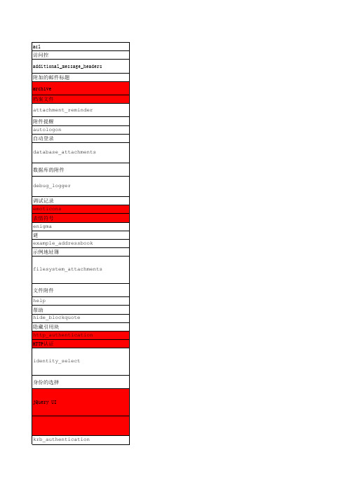
IMAP Folders Access Control Lists Management (RFC4314, RFC2086). IMAP文件夹的访问控制列表管理(rfc4314,rfc2086)。 ery simple plugin which will add additional headers to or remove them from outgoing messages. 非常简单的插件,将添加额外的头或从传出的消息删除它们。 his adds a button to move the selected messages to an archive folder. The folder (and the optional structure of subfolders) can be selected in the settings panel. 他添加了一个按钮,将选定的消息移动到存档文件夹。文件夹(子文件夹结构和可选)可以在设置面板中选择。 This Roundcube plugin reminds the user to attach a file if the composed message text indicates that there should be any. 这Roundcube插件让用户如果组成消息文本表明,应该有任何附加文件。 Sample plugin to try out some hooks 示例插件尝试一些钩子 This plugin which provides database backed storage for temporary attachment file handling. The primary advantage of this plugin is its compatibility with round-robin dns multi-server Roundcube installations. 此插件为临时附件文件处理提供数据库支持的存储。这个插件的主要优点是用循环DNS的多服务器RoundCube装置 的相容性。 Enhanced logging for debugging purposes. It is not recommened to be enabled on production systems without testing because of the somewhat increased memory, cpu and disk i/o overhead. 用于调试目的的增强日志。它是不适合被启用生产系统没有测试因为有些增加内存、CPU和磁盘I/O开销。 Plugin that adds emoticons support. 插件添加表情符号的支持。 PGP Encryption for Roundcube Roundcube加密为PGP Sample plugin to add a new address book with just a static list of contacts 用一个静态联系人列表添加新地址簿的示例插件 This is a core plugin which provides basic, filesystem based attachment temporary file handling. This includes storing attachments of messages currently being composed, writing attachments to disk when drafts with attachments are re-opened and writing attachments to disk for inline display in current html compositions. 这是一个提供基本的基于文件系统的附件临时文件处理的核心插件。这包括存储当前正在组成的邮件的附件,当附 加附件的草稿被重新打开并在当前HTML组合物中对磁盘进行写入时,将附件写入磁盘。 Plugin adds a new item (Help) in taskbar. 插件在任务栏添加新项目(帮助)。 This allows to hide long blocks of cited text in messages. 这允许在消息中隐藏被引文本的长块。 HTTP Basic Authentication HTTP基本认证 On reply to a message user identity selection is based on content of standard headers like From, To, Cc and Return-Path. Here you can add header(s) set by your SMTP server (e.g. Delivered-To, Envelope-To, X-Envelope-To, X-RCPT-TO) to make identity selection more accurate. 在回复消息时,用户身份选择基于诸如从,到,CC和返回路径的标准报头的内容。你可以在这里添加标题(S)设 置SMTP服务器(例如交付,信封,x-envelope-to,x-rcpt-to)进行身份选择更准确。 Plugin adds the complete jQuery-UI library including the smoothness theme to Roundcube. This allows other plugins to use jQuery-UI without having to load their own version. The benefit of using one central jQuery-UI is that we wont run into problems of conflicting jQuery libraries being loaded. All plugins that want to use jQuery-UI should use this plugin as a requirement. 完整的jQuery插件adds the Library including the theme(IU)roundcube光滑。使用jQuery插件allows other to this to their IU没有过负荷-自己的版本。的好处,使用一个中央of the is that we jQuery -我也` IU学 院图书馆conflicting jQuery遇见问题被加载。我使用jQuery的插件,这个插件应该使用AS - IU在需求 N/A
北京亚控 工业自动化通用组态软件 组态王 version 6.51 命令语言函数 速查手册

工业自动化通用组态软件组态王version 6.51命令语言函数速查手册北京亚控科技发展有限公司前言本手册为北京亚控科技发展有限公司组态王6.51软件《组态王6.51使用手册》的辅助说明,主要详细介绍组态王6.51软件中提供的命令语言函数的定义和使用方法。
手册中提供的信息为产品发布时软件的相关使用信息,如有变化,恕不另行通知。
亚控公司不能保证手册中没有错误。
在没有亚控公司书面允许的前提下,除购买者自己使用外,不得为任何其他目的、使用任何方法(包括复印和录制在内的电子和机械手段)对本手册的任何部分的内容进行复制和传播。
如果您在使用本手册的过程中发现了问题,请以书面的形式把它记录下来,并与我们取得联系,亚控公司表示衷心的感谢。
《组态王6.51命令语言函数速查手册》2005 亚控公司 著作权所有,保留所有权利版本号:6.5.1.3亚控公司技术支持热线:电话:010-82616619E-Mail:support@sales@或通过网站与我们联系:组态王命令语言速查手册目录 1目录Abs (1)Ack (1)ActivateApp (1)ArcCos (2)ArcSin (2)ArcTan (3)Average (3)BackUpHistData (4)Bit (4)BitSet (5)ChangePassword (5)chartAdd (6)chartClear (6)chartSetBarColor (7)chartSetValue (8)ClosePicture (8)Cos (9)Date (9)DisplayMCI (9)Dtext (10)EditUsers (10)Exit (11)Exp (11)FileCopy (11)FileDelete (13)FileMove (13)FileReadFields (15)FileReadStr (16)北京亚控科技发展有限公司2组态王命令语言速查手册目录FileWriteFields (17)FileWriteStr (18)GetBackupProgress (18)GetDate (19)GetGroupName (20)GetKey (20)GetStationStatus (20)GetTime (21)HidePicture (21)HTConvertTime (22)HTGetPenName (23)HTGetPenRealValue (23)HTGetTimeAtScooter (24)HTGetTimeStringAtScooter (25)HTGetValue (26)HTGetValueAtScooter (27)HTGetValueAtZone (27)HTScrollLeft (28)HTScrollRight (29)HTSetLeftScooterTime (29)HTSetPenName (30)HTUpdateToCurrentTime (30)HTZoomIn (31)HTZoomOut (32)InfoAppActive (32)InfoAppDir (33)InfoAppTitle (33)InfoDisk (34)InfoFile (34)InfoResource (35)Int (36)北京亚控科技发展有限公司组态王命令语言速查手册目录 3 listLoadList (36)listSaveList (37)listAddItem (38)listClear (38)listDeleteItem (39)listDeleteSelection (39)listFindItem (40)listGetItem (40)listGetItemData (41)listInsertItem (42)listSetItemData (42)ListLoadFileName (43)LoadDriverConfig (43)LoadText (44)LogE (45)LogN (45)LogOff (45)LogOn (46)LogString (46)Max (47)Min (47)MovePicture (47)PageDown (48)PageUp (48)PI (48)PlayAvi (48)PlaySound (49)PlaySound2 (50)Pow (50)PowerCheckUser (51)PrintWindow (52)北京亚控科技发展有限公司4组态王命令语言速查手册目录pvAddNewRealPt (53)pvAddNewSetPt (56)pvClear (57)pvGetValue (57)pvIniPreCuve (58)pvLoadData (60)pvModifyPreValue (62)pvMoveSlide (62)pvSaveData (63)pvSetLimits (64)ReadTag (65)ReBuildDDE (66)ReBuildUnConnectDDE (66)RecipeDelete (66)RecipeInsertRecipe (67)RecipeLoad (67)RecipeSave (68)RecipeSelectNextRecipe (68)RecipeSelectPreviousRecipe (69)RecipeSelectRecipe (69)Report1 (70)Report2 (71)ReportPrint (71)ReportPrint2 (72)ReportPrintSetup (73)ReportGetCellString (73)ReportGetCellValue (74)ReportGetColumns (74)ReportGetRows (75)ReportLoad (75)ReportPageSetup (75)北京亚控科技发展有限公司组态王命令语言速查手册目录 5 ReportSaveAs (76)ReportSetCellString (76)ReportSetCellString2 (77)ReportSetCellValue (78)ReportSetCellValue2 (79)ReportSetHistData (80)ReportSetHistData2 (81)ReportWebDownload (81)SampleVar (82)SampleVarEnd (83)SaveText (83)SendKeys (83)SetTrendPara (86)Sgn (86)ShowPicture (87)Sin (87)SQLAppendStatement (87)SQLClearStatement (88)SQLClearTable (88)SQLCommit (88)SQLConnect (89)SQLCreateTable (90)SQLDelete (90)SQLDisconnect (91)SQLDropTable (91)SQLEndSelect (92)SQLErrorMsg (92)SQLExecute (93)SQLFirst (93)SQLGetRecord (94)SQLInsert (94)北京亚控科技发展有限公司6组态王命令语言速查手册目录SQLInsertEnd (95)SQLInsertExecute (95)SQLInsertPrepare (96)SQLLast (96)SQLLoadStatement (96)SQLNext (97)SQLNumRows (97)SQLPrepareStatement (98)SQLPrev (98)SQLRollback (98)SQLSelect (99)SQLSetParamChar (101)SQLSetParamDate (102)SQLSetParamDateTime (102)SQLSetParamDecimal (103)SQLSetParamTime (103)SQLSetParamFloat (103)SQLSetParamInt (104)SQLSetParamNull (105)SQLSetStatement (105)SQLTransact (106)SQLUpdate (106)SQLUpdateCurrent (107)Sqrt (107)StartApp (107)StrASCII (108)StrChar (108)StrFromInt (109)StrFromReal (109)StrFromTime (110)StrInStr (111)北京亚控科技发展有限公司组态王命令语言速查手册目录7 StrLeft (111)StrLen (112)StrLower (112)StrMid (113)StrReplace (113)StrRight (114)StrSpace (115)StrToInt (115)StrToReal (116)StrTrim (116)StrType (117)StructVarRefAddress (118)StrUpper (119)StopBackupStation (120)Sum (120)Tan (120)Text (121)Time (121)Trace (121)Trunc (122)VarRefAddress (123)xyAddNewPoint (124)xyClear (124)亚控公司各地分支机构联系方式: (126)北京亚控科技发展有限公司命令语言函数速查手册“组态王”支持使用内建的复杂函数,其中包括字符串函数、数学函数、系统函数、控件函数、报表函数及其他函数,下面依次介绍各个函数(函数名不区分大小写,按字母排序):Abs此函数用于计算变量值的绝对值,使用格式如下:Abs(变量名或数值);返回值:整值或实型值;例如:Abs(14); 返回值为14Abs(-7.5); 返回值为7.5Abs(距离); 返回内存模拟变量“距离”的绝对值。
rfc相关设置及使用

rfc相关设置及使用RFC(Request for Comments)是一种用于定义互联网协议、标准和相关问题的文档。
RFC的格式由互联网工程任务组(IETF)统一规定,它们记录了网络技术的发展和演进过程。
在本文中,我们将介绍RFC相关的设置和使用。
1. 了解RFC的作用和历史:RFC是由IETF组织制定的一种标准化文档,它记录了互联网协议的设计、开发和演化过程。
RFC起源于20世纪60年代的ARPANET,是一种社区驱动的文档,通过共享和讨论来推动互联网技术的发展。
RFC文档旨在提供指南、建议和最佳实践,帮助网络技术人员解决问题。
2. 寻找和阅读RFC文档:RFC文档可以在互联网上免费获取,IETF的官方网站和其他资源库都有存档。
这些文档按照顺序编号,并且以RFC开头,比如RFC 791定义了IPv4协议。
通过搜索引擎或在IETF网站上使用关键词搜索,可以找到特定主题的RFC文档。
阅读RFC文档时,应该注意文档的状态,有一些可能已经被更新或废弃。
3. 使用RFC文档:RFC文档在网络技术的发展过程中起着重要的指导作用。
它们提供了协议规范、算法实现、安全性和隐私等方面的建议。
网络管理员、网络工程师和开发人员可以使用RFC文档来了解和理解特定协议或标准的设计原理和要求。
此外,RFC文档还常用于进行互联网协议的实现、编程和配置。
4. 参与RFC的制定过程:RFC并不是静止的文件,而是一个持续演进的过程。
任何人都可以参与到RFC的制定过程中。
要参与RFC的制定,可以加入IETF并参与相关的工作组或邮件列表。
通过这种方式,个人可以提出改进建议,参与讨论和标准化的制定。
5. 遵循RFC的指导原则:在网络技术领域,遵循RFC的指导原则是至关重要的。
这些指导原则包括设计原则、协议分层、安全性和互操作性等要求。
遵循RFC的指导原则可以确保网络协议的正确性、稳定性和可靠性,同时也可以促进网络技术的发展和创新。
总结起来,RFC在互联网技术领域起着重要的作用,它们记录了互联网协议的发展历程和指导原则。
rfc算法原理
rfc算法原理RFC(Request for Comments)算法是一种用于计算哈希值的算法。
该算法的设计目标是快速计算出哈希值,并且能够保持较低的冲突率。
本文将介绍RFC算法的原理及其在实际应用中的一些特点和优势。
RFC算法的原理基于位运算和循环移位操作。
它采用了一种迭代的方式,通过对输入数据的每个字节进行一系列的位操作来计算出哈希值。
具体来说,RFC算法将输入数据按字节逐个处理,然后利用位运算和循环移位操作对每个字节进行处理,并最终得到一个32位的哈希值。
在RFC算法中,每个字节都会与一个32位的初始值进行异或操作。
这个初始值可以是一个随机数,也可以是一个固定的值。
通过不断进行异或操作,每个字节都会对哈希值产生影响,从而使哈希值能够充分地反映输入数据的特征。
除了异或操作之外,RFC算法还会对每个字节进行位运算和循环移位操作。
这些操作可以有效地改变字节的顺序和位置,从而进一步增加哈希值的随机性。
通过这些位运算和循环移位操作,RFC算法能够在保持较低的冲突率的同时,快速计算出哈希值。
RFC算法在实际应用中具有一些特点和优势。
首先,RFC算法的计算速度非常快。
由于它采用了位运算和循环移位操作,而不是复杂的数学运算,所以可以在很短的时间内计算出哈希值。
这使得RFC 算法非常适合在计算资源受限的环境下使用。
RFC算法的冲突率相对较低。
通过对每个字节进行一系列的位运算和循环移位操作,RFC算法能够充分地利用输入数据的特征,从而降低哈希值的冲突率。
这使得RFC算法在数据存储和索引等领域具有广泛的应用。
RFC算法还具有较好的扩展性和灵活性。
由于RFC算法只对输入数据的每个字节进行处理,所以可以很方便地将其应用于不同类型的数据,如文本、图像、音频等。
同时,RFC算法也可以根据具体应用的需求进行调整和优化,以提高哈希值的计算效率和冲突率。
总结起来,RFC算法是一种用于计算哈希值的快速算法。
它通过位运算和循环移位操作,对输入数据的每个字节进行处理,并最终得到一个32位的哈希值。
开源项目rfc流程

开源项目rfc流程开源项目RFC流程1. 什么是RFC?•RFC是”Request for Comments”的缩写,意为”征求意见”或”意见征集”。
•在开源项目中,RFC是一种协作流程,用于提出新的功能或更改现有功能的建议,并征求项目群体的意见。
2. RFC的目的与重要性•RFC流程为开源项目提供了一个包容性的环境,让所有人都有机会参与决策过程。
•通过RFC流程,项目团队可以更好地理解社区成员的需求,减少冲突和误解,并确保变更是基于共识和讨论的结果。
3. RFC流程的具体步骤•提出RFC:在项目的RFC存储库中创建一个新的RFC文件,并使用Markdown格式编写提案。
•反馈与讨论:项目群体和有兴趣的社区成员将参与讨论,提出问题、建议和其他反馈。
•修改与改进:根据收到的反馈,作者可以对RFC进行修改和改进,以更好地满足需求和解决问题。
•状态更新:在RFC的生命周期中,通过更新RFC文件的状态,作者可以向社区反馈进展情况。
•最终评审:项目核心团队将对RFC进行最终评审,并确认是否接受或拒绝提案。
•实施与跟踪:一旦RFC被接受并实施,作者需要跟踪变更的进展,并确保及时更新相关文档。
4. RFC文章的Markdown格式要求•使用Markdown格式可以更好地展示RFC的内容和结构。
•下面提供一些常用的Markdown格式要求:–标题:使用井号(#)表示不同级别的标题,以突出重点和组织结构。
–列表:使用横杠(-)或星号(*)创建无序列表,使用数字创建有序列表。
–引用:使用大于号(>)创建引用段落,用于引用他人意见或讨论。
–代码块:使用反引号(`)创建代码块,用于展示代码示例或命令。
–链接:使用方括号([])和圆括号(())创建链接,以便在RFC中引用其他文件或资源。
5. 一些建议与注意事项•清晰明了地描述问题或需求,以便社区成员更好地理解和提供反馈。
•避免使用复杂的排版和格式,以保持RFC的易读性。
- 1、下载文档前请自行甄别文档内容的完整性,平台不提供额外的编辑、内容补充、找答案等附加服务。
- 2、"仅部分预览"的文档,不可在线预览部分如存在完整性等问题,可反馈申请退款(可完整预览的文档不适用该条件!)。
- 3、如文档侵犯您的权益,请联系客服反馈,我们会尽快为您处理(人工客服工作时间:9:00-18:30)。
Network Working Group J. Strombergson Request for Comments: 4194 InformAsic AB Category: Standards Track L. Walleij Lunds Tekniska Hogskola P. Faltstrom Cisco Systems Inc October 2005 The S Hexdump FormatStatus of this MemoThis document specifies an Internet standards track protocol for the Internet community, and requests discussion and suggestions forimprovements. Please refer to the current edition of the "InternetOfficial Protocol Standards" (STD 1) for the standardization stateand status of this protocol. Distribution of this memo is unlimited.Copyright NoticeCopyright (C) The Internet Society (2005).AbstractThis document specifies the S Hexdump Format (SHF), a new, XML-based open format for describing binary data in hexadecimal notation. SHF provides the ability to describe both small and large, simple andcomplex hexadecimal data dumps in an open, modern, transport- andvendor-neutral format.1. IntroductionIn the computing, network, and embedded systems communities, several different types of data formats for hexadecimal data are being used. One of the more common formats is known as "S-records" (and severalderivatives), which reportedly originated at the Motorola company.The S Hexdump Format is named in its honour.Typical uses of these dump formats include executable object code for embedded systems (i.e., "firmware"), on-chip flash memories andfilesystems, FPGA configuration bitstreams, graphics and otherapplication resources, routing tables, etc. Unfortunately, none ofthe formats used are truly open, vendor-neutral, and/or well-defined.Even more problematic is the fact that none of these formats are able to represent the large data sizes that are getting more and morecommon. Data dumps comprised of multiple sub-blocks with different Strombergson, et al. Standards Track [Page 1]Word sizes, and data sizes spanning anywhere from a few Bytes of data to much larger than 2^32 bits are not handled. Also, the checksumsincluded in these formats are too simplistic and for larger datasizes, they provide insufficient ability to accurately detect errors. Alternatively, the overhead needed for proper error detection is very large.Therefore, the S Hexdump format is an effort to provide a modern,XML-based format that is not too complex for simple tools andcomputing environments to implement, generate, parse, and use. Yetthe format is able to handle large data sizes and complex datastructures, and can provide high quality error detection byleveraging standardized cryptographic hash functions.One of the simplifications introduced in the format is to disallowother number systems such as octal or decimal notation, and to allow for Word sizes of even bytes (8-bit groups) only. This isintentional and was done to simplify implementations aimed forpractical present-day applications. Formats aimed for esotericnumber systems or odd Word sizes may be implemented elsewhere.At present, the usage of the SHF format may be mainly for Internettransport and file storage on development machinery. A parser forthe XML format is presently not easily deployed in hardware devices, but the parsing and checksumming of the SHF data may be done by aworkstation computer, which in turn converts the SHF tokens to anordinary bitstream before the last step (e.g., of a firmware upgrade) commences.SHF is a dump format only and shall not be confused with similarapplications, such as binary configuration formats or patches, which are intended to, for example, alter contents of a core memory. Such applications require the possibility of modifying individual bits or groups of bits in the memory of a machine, and is not the intendedusage of the mechanism described in the present document.2. TerminologyThe key words "MUST", "MUST NOT", "REQUIRED", "SHALL", "SHALL NOT","SHOULD", "SHOULD NOT", "RECOMMENDED", "MAY", and "OPTIONAL" in this document are to be interpreted as described in RFC 2119 [1].The key word "Byte" is to be interpreted as a group of 8 bits. Thekey word "Octet" is another name for Byte.The key word "Word" is to be interpreted as a group containing anintegral number of Bytes.Strombergson, et al. Standards Track [Page 2]The key word "Block" is to be interpreted as an ordered sequence ofWords, beginning at a certain address, running from lower to higheraddresses. A Block typically represents a sequence of Words at acertain address range in the memory of a computer.The key word "Dump" is to be interpreted as a sequence of Blocks,which may or may not be in a particular order. A Dump typicallyrepresents some non-continuous, interesting parts of the memory of a computer, such that the Dump as a whole has a certain meaning, forexample (but not limited to) a complete firmware for an embeddedsystem.The expression "2^n" is to be interpreted as the value two (2) raised to the n:th power. For example, 2^8 equals the value 256.3. Features and FunctionalityThe SHF-format has the following features:o Support for arbitrarily wide data Wordso Support for very large data Blockso Support for an arbitrary number of independent data Blockso Data integrity detection against errors provided by the RFC3174specified (see [2]) SHA-1 cryptographic signatureo An XML-based formatIn the embedded systems domain, 8- and 16-bit processors are stillused in large numbers and will continue to be used for anyforeseeable future. Simultaneously, more and more systems are using 64-bit and even larger Word sizes.SHF supports all of these systems by allowing the Word size to bespecified. The Word size MUST be an integer number of Bytes and atleast one (1) Byte.SHF is able to represent both large and small data Blocks. The data Block MUST contain at least one (1) Word. Additionally, the dataBlock MUST NOT be larger than (2^64)-1 bits.The SHF Dump MUST contain at least one (1) data Block. The maximumnumber of Blocks supported is 2^64. Each data Block in the Dump MAY have different Word sizes and start at different addresses. Strombergson, et al. Standards Track [Page 3]The checksum (or message digest) used to verify the correctness ordata integrity of each Block is 20 Bytes (160 bits) long. The digest MUST be calculated on the data actually represented by the SHF dataBlock, NOT the representation, i.e., NOT the ASCII-code. SHA-1 isonly able to calculate a digest for a data Block no larger than(2^64)-1 bits and this limits the size of each data Block in SHF to(2^64)-1 bits.4. SHF XML SpecificationThe SHF format consists of an XML data structure representing a Dump. The Dump consists of a Dump header section and one (1) or more Block sections containing data. Each Block of data is independent of anyother Block.A short, symbolic example of an SHF Dump is illustrated by thefollowing structure:<dump name="(Human readable string)" blocks="(64-bit value)"><block name="(Human readable string)" start_address="(64-bitvalue)" word_size="(64-bit value)" length="(64-bit value)"checksum="(20-Byte digest)">(Data)</block></dump>4.1. Header SectionThe header section comprises the Dump tag, which includes thefollowing attributes:o name: A compulsory string of arbitrary length used by anyinterested party to identify the specific SHF Dump.o blocks: An optional 64-bit hexadecimal value representing thenumber of Blocks in the specific SHF Dump. Whenever available,this value should be supplied. However, there are potentialscenarios where the number of Blocks cannot be given beforehand.If the value is present, it should be verified by implementers; if the value is untrue, the behaviour is implementation-defined.After the opening Dump tag, one or more subsections of Blocks mustfollow. Finally, the complete SHF Dump ends with a closing Dump tag. Strombergson, et al. Standards Track [Page 4]4.2. Block SubsectionThe Block subsection contains a Block tag and a number of data words. The Block tag includes the following attributes:o name: A compulsory string of arbitrary length used by anyinterested party to identify the specific Block.o start_address: A compulsory, 64-bit hexadecimal value representing the start address in Bytes for the data in the Block.o word_size: A compulsory 64-bit hexadecimal value representing the number of Bytes (the width) of one Word of the data.o length: A compulsory hexadecimal representation of an unsigned64-bit integer indicating the number of Words following inside the Block element. If this value turns out to be untrue, the BlockMUST be discarded.o checksum: A compulsory hexadecimal representation of the 20 ByteSHA-1 digest of the data in the Block.The total size of the data in the Block (in bits) is given by theexpression (8 * word_size * length). The expression MUST NOT belarger than (2^64)-1.After the opening Block tag, a hexadecimal representation of theactual data in the Block follows. Finally, the Block section endswith a closing Block tag.5. SHF Rules and LimitsThere are several rules and limits in SHF:o All attribute values representing an actual value and the dataMUST be in hexadecimal notation. The only attribute excluded from this rule is the name attribute in the Dump and Block tags. This restriction has been imposed for ease of reading the dump: areader shall not be uncertain about whether a figure is in hexnotation or not, and can always assume it is hexadecimal.o All attribute values, with the exception of the checksum, MAY omit leading zeros. Conversely, the checksum MUST NOT omit leadingzeros.o The data represented in a Block MUST NOT be larger than (2^64)-1bits.Strombergson, et al. Standards Track [Page 5]o The size of a Word MUST NOT be larger than (2^64)-1 bits. Thisimplies that a Block with a Word defined to the maximum widthcannot contain more than one Word. An SHF consumer shall assurethat it can handle a certain Word length before beginning to parse blocks of an SHF Dump. Failure to do so may cause bufferoverflows and endanger the stability and security of the systemrunning the consuming application.o The attribute values representing an actual value MUST be inbig-endian format. This means that the most significanthexadecimal digits are to be put to the left in a hexadecimalWord, address, or similar field. For example, the address value1234 represents the address 1234 and not 3412. While somecomputing architectures may be using little-endian Words as their native format, it is the responsibility of any SHF producerrunning on such an architecture to swap the attribute values to a big-endian format. The reverse holds for a consumer receiving the big-endian SHF attributes: if the consumer is little-endian, thevalues have to be swapped around.o Likewise, the words inside a Dump MUST be stored in a big-endianformat if the word size is larger than one Byte. Here, the sameneed for swapping Bytes around may arise, as mentioned in theprevious paragraph.6. SHF DTDThe contents of the element named "block" and the attributes"blocks", "address", "word_size" and "checksum" should only containthe characters that are valid hexbyte sequences. These are:whitespace ::= (#x20 | #x9 | #xC | #xD | #xA)hexdigit ::= [0-9A-Fa-f]hexbytes ::= whitespace* hexdigit (hexdigit|whitespace)*A parser reading in an SHF file should silently ignore any othercharacters that (by mistake) appear in any of these elements orattributes. These alien characters should be treated as if they did not exist. Also note that "whitespace" has no semantic meaning; itis only valid for the reason of improving the human readability ofthe Dump. Whitespace may be altogether removed and the hexbytesequences concatenated if desired. Notice that the fact that wordsize is to be given in a number of bytes implies that the number ofhexadecimal digits inside a block need to be even. Malformed blocks should be ignored by implementations.Strombergson, et al. Standards Track [Page 6]<!--DTD for the S Hexdump Format, as of 2003-10-10Linus Walleij, Joachim Strombergson, Patrik Faltstrom 2003Refer to this DTD as:<!ENTITY % SHF PUBLIC "-//IETF//DTD SHF//EN""/dtd/shf.dtd">%SHF;--><?xml version="1.0" encoding="UTF-8"?><!ELEMENT dump (block)+><!ATTLIST dumpname CDATA #REQUIREDblocks CDATA #IMPLIED><!ELEMENT block (#PCDATA)><!ATTLIST blockname CDATA #REQUIREDaddress CDATA #REQUIREDword_size CDATA #REQUIREDlength CDATA #REQUIREDchecksum CDATA #REQUIRED>7. SHF ExamplesThis section contains three different SHF examples, illustrating the usage of SHF and the attributes in SHF.The first example is a simple SHF Dump with a single Block of data:<?xml version="1.0" encoding="UTF-8"?><dump name="Simple SHF example" blocks="01"><block name="Important message in hex format" address="0400"word_size="01" length="1f"checksum="5601b6acad7da5c7b92036786250b053f05852c3">41 6c 6c 20 79 6f 75 72 20 62 61 73 65 20 61 7265 20 62 65 6c 6f 6e 67 20 74 6f 20 75 73 0a</block></dump>Strombergson, et al. Standards Track [Page 7]The second example is a program in 6502 machine code residing atmemory address 0x1000, which calculates the 13 first Fibonaccinumbers and stores them at 0x1101-0x110d:<?xml version="1.0" encoding="UTF-8"?><dump name="6502 Fibonacci" blocks="02"><block name="Code" address="1000" word_size="01" length="2a"checksum="5cab5bf8ee299af1ad17e8093d941914eb5930c7">a9 01 85 20 85 21 20 1e 10 20 1e 10 18 a5 21 aa65 20 86 20 85 21 20 1e 10 c9 c8 90 ef 60 ae 0011 a5 21 9d 00 11 ee 00 11 60</block><block name="Mem" address="1100" word_size="01" length="e"checksum="c8c2001c42b0226a5d9f7c2f24bd47393166487a">01 00 00 00 00 00 00 00 00 00 00 00 00 00</block></dump>The final example contains a Block of 40-bit wide data:<?xml version="1.0" encoding="UTF-8"?><dump name="Example of an SHF dump with wide data words" blocks="00001"> <block name="SMIL memory dump" address="000" word_size="5"length="1A" checksum="ff2033489aff0e4e4f0cd7901afc985f7a213c97"> 00100 00200 00000 00090 00000 00036 00300 0040000852 00250 00230 00858 00500 00600 014DC 00058002A8 000B8 00700 00800 000B0 00192 00100 0000000900 00A00 00000 0000A 40000 00000 00B00 00C0000000 00000 00000 00001 00D00 00E00 00000 001000CCCC CCCCD 00F00 01000 00000 00010 80000 0000000100 00790 00000 00234</block></dump>8. SHF Security ConsiderationsThe SHF format is a format for representing hexadecimal data that one wants to transfer, manage, or transform. The format itself does not guarantee that the represented data is not falsely represented,malicious, or otherwise dangerous.The data integrity of the SHF file as a whole is to be provided, ifneeded, by means external to the SHF file, such as the genericsigning mechanism described by RFC 3275 [3].Strombergson, et al. Standards Track [Page 8]9. IANA ConsiderationsThis section contains the registration information for the MIME type to SHF. The media type has been chosen to comply with the guidelines in [4].o Registration: application/shf+xmlo MIME media type name: applicationo MIME subtype name: shf+xmlo Required parameters: charsetRequired parameters: charsetThis parameter must exist and must be set to "UTF-8". No othercharacter sets are allowed for transporting SHF data. The character set designator MUST be uppercase.Encoding considerations:This media type may contain binary content; accordingly, when usedover a transport that does not permit binary transfer, an appropriate encoding must be applied.Security considerations:A hex Dump in itself has no other security considerations than whatapplies for any other XML file. However, the included binary datamay in decoded form contain any executable code for a targetplatform. If additional security is desired, additional transportsecurity solutions may be applied. For target code contained in ahex Dump, developers may want to include certificates, checksums, and the like in hexdump form for the target platform. Such uses areoutside the scope of this document and a matter of implementation.Interoperability considerations:n/aPublished specification:This media type is a proper subset of the XML 1.0 specification [5]. One restriction is made: no entity references other than the fivepredefined general entities references ("&", "<", ">","'", and """) and numeric entity references may be present. Neither the "XML" declaration (e.g., <?xml version="1.0" ?>) nor the "DOCTYPE" declaration (e.g., <!DOCTYPE ...>) need be present. (XMLfragments are allowed.) All other XML 1.0 instructions (e.g., CDATA blocks, processing instructions, and so on) are allowed. Strombergson, et al. Standards Track [Page 9]Applications that use this media type: any program or individualwishing to make use of this XML 1.0 subset for hexdump exchange.Additional information:o Magic number: There is no single initial Byte sequence that isalways present for SHF fileso File extension: shfo Macintosh File Type code: noneIntended usage: COMMON.Author/Change controller: this MIME transport type is controlled bythe IETF.10. ExtensionsThe attributes of elements in the SHF XML format may be extended when need arises. For example, certain applications will want torepresent executable code as an SHF Dump, and may then need anexecution start address to be associated with certain Dump Blocks, so that the address can be configured as a starting point for the CPUpart of any processor code present in the Block, as opposed to theraw data, which is already given a start address by way of the"address" attribute. This can be done by extending the Block tagwith a "start_address" attribute.Another possible scenario is when a dump is applied to a computersystem with several independent address spaces, such as a system with two CPUs, each with independent memories. In this case, a user maywant to add an "address_space" attribute.As long as such new attributes are added, with no attributes beingremoved or redefined, the resulting Dump shall be considered a valid SHF Dump and transported using the application/xml+shf transporttype. Parsers unaware of the modified namespace shall silentlyignore any such extended attributes, or simply duplicate them frominput to output when processing an SHF file as a filter. Themanagement of such extended attributes is a matter of conventionbetween different classes of users and not a matter of the IETF. Strombergson, et al. Standards Track [Page 10]11. Additional InformationContact for further information: c.f., the "Authors’ Addresses"section of this memo.Acknowledgements: The SMIL memory Dump was kindly provided by StenHenriksson at Lund University. Proofreading and good feedback on the SHF document was generously provided by Peter Lindgren, Tony Hansen, Larry Masinter, and Clive D.W. Feather. We also want to thank theApplications area workgroup for their help during development.12. Normative References[1] Bradner, S., "Key words for use in RFCs to Indicate Requirement Levels", BCP 14, RFC 2119, March 1997.[2] Eastlake, 3rd, D. and P. Jones, "US Secure Hash Algorithm 1(SHA1)", BCP 14, RFC 3174, September 2001.[3] Eastlake, 3rd, D., Joseph, J., and D. David, "(Extensible Markup Language) XML-Signature Syntax and Processing", BCP 14,RFC 3275, March 2002.[4] Makoto, M., Simon, S., and D. Dan, "(Extensible Markup Language) XML Media Types", RFC 3023, January 2001.[5] Bray, Tim, Paoli, Jean, Sperberg-McQueen, C. M. and Maler, Eve, Yergeau, Francois, "Extensible Markup Language (XML) 1.0 (Third Edition)", /TR/REC-xml.Strombergson, et al. Standards Track [Page 11]Authors’ AddressesJoachim StrombergsonInformAsic ABHugo Grauers gata 5aGothenburg 411 33SEPhone: +46 31 68 54 90EMail: Joachim.Strombergson@URI: /Linus WalleijLunds Tekniska HogskolaMaster Olofs Vag 24Lund 224 66SEPhone: +46 703 193678EMail: triad@df.lth.sePatrik FaltstromCisco Systems IncLedasa273 71 LovestadSwedenEMail: paf@URI: Strombergson, et al. Standards Track [Page 12]Full Copyright StatementCopyright (C) The Internet Society (2005).This document is subject to the rights, licenses and restrictionscontained in BCP 78, and except as set forth therein, the authorsretain all their rights.This document and the information contained herein are provided on an "AS IS" basis and THE CONTRIBUTOR, THE ORGANIZATION HE/SHE REPRESENTS OR IS SPONSORED BY (IF ANY), THE INTERNET SOCIETY AND THE INTERNETENGINEERING TASK FORCE DISCLAIM ALL WARRANTIES, EXPRESS OR IMPLIED,INCLUDING BUT NOT LIMITED TO ANY WARRANTY THAT THE USE OF THEINFORMATION HEREIN WILL NOT INFRINGE ANY RIGHTS OR ANY IMPLIEDWARRANTIES OF MERCHANTABILITY OR FITNESS FOR A PARTICULAR PURPOSE. Intellectual PropertyThe IETF takes no position regarding the validity or scope of anyIntellectual Property Rights or other rights that might be claimed to pertain to the implementation or use of the technology described inthis document or the extent to which any license under such rightsmight or might not be available; nor does it represent that it hasmade any independent effort to identify any such rights. Information on the procedures with respect to rights in RFC documents can befound in BCP 78 and BCP 79.Copies of IPR disclosures made to the IETF Secretariat and anyassurances of licenses to be made available, or the result of anattempt made to obtain a general license or permission for the use of such proprietary rights by implementers or users of thisspecification can be obtained from the IETF on-line IPR repository at /ipr.The IETF invites any interested party to bring to its attention anycopyrights, patents or patent applications, or other proprietaryrights that may cover technology that may be required to implementthis standard. Please address the information to the IETF at ietf-ipr@.AcknowledgementFunding for the RFC Editor function is currently provided by theInternet Society.Strombergson, et al. Standards Track [Page 13]。