APM2301CA中文资料
ST2301中文资料

-2.8ADESCRIPTIONThe ST2301 is the P-Channel logic enhancement mode power field effect transistor are produced using high cell density, DMOS trench technology.This high density process is especially tailored to minimize on-state resistance.These devices are particularly suited for low voltage application such as cellular phone and notebook computer power management and other batter powered circuits, and low in-line power loss are needed in a very small outine surface mount package.PIN CONFIGURATION SOT-23-3L1.Gate2.Source3.DrainS: Subcontractor Y: Year Code A: Process CodeFEATUREz -20V/-2.8A, R DS(ON) = 120m-ohm@VGS = -4.5Vz -20V/-2.0A, R DS(ON) = 170m-ohm@VGS = -2.5Vz Super high density cell design forextremely low R DS(ON)z Exceptional on-resistance and maximumDC current capabilityz SOT-23-3L package design-2.8AABSOULTE MAXIMUM RATINGS (Ta = 25J Unless otherwise noted )Parameter Symbol Typical Unit Drain-Source Voltage V DSS -20 V Gate-Source VoltageV GSS +12V Continuous Drain Current (TJ=150J ) T A =25¢JT A =70J I D-2.5 -1.5A Pulsed Drain CurrentI DM -10 A Continuous Source Current (Diode Conduction) I S -1.6 A Power DissipationT A =25¢J T A =70JP D 1.250.8W Operation Junction Temperature T J 150 J Storgae Temperature RangeT STG -55/150 J Thermal Resistance-Junction to AmbientR cJA 120J /W-2.5AELECTRICAL CHARACTERISTICS ( Ta = 25J Unless otherwise noted )Parameter Symbol Condition Min Typ Max UnitStaticDrain-Source Breakdown Voltage V (BR)DSS V GS =0V,I D =-250uA -20VGate Threshold Voltage V GS(th) V DS =V GS ,I D =-250uA -0.45 -1.5VGate Leakage CurrentI GSS V DS =0V,V GS =+8V +100nAV DS =-30V,V GS =0V -1Zero Gate Voltage Drain CurrentI DSS V DS =-30V,V GS =0V T J =55J-10uAOn-State Drain Current I D(on) V DS -5V,V GS =-4.5V V DS -5V,V GS =-2.5V -6 -3ADrain-source On-Resistance R DS(on)V GS =-4.5V,I D =-2.8AV GS =-2.5V,I D =-2.0A0.09 0.1450.120.17Forward Transconductance g fsV DS =-5V,I D =-2.8V 6.5 S Diode Forward Voltage V SD I S =-1.6A,V GS =0V -0.8 -1.2VDynamicTotal Gate Charge Qg 5.8 10 Gate-Source Charge Qgs 0.85Gate-Drain Charge Qgd V DS =-6V,V GS =-4.5VI D -2.8A 1.7nC Input Capacitance Ciss 415Output CapacitanceCoss 223Reverse Transfer Capacitance CrssV DS =-6V,V GS =0VF=1MHz 23pF 13 25Turn-On Timet d(on) t r 36 60 42 70 Turn-Off Timet d(off) t fV DD =-6V,R L =6 I D =-1A,V GEN =-4.5VR G =634 60nS-2.5ASOT-23-3L PACKAGE OUTLINE-2.5ATYPICAL CHARACTERICTICS (25J Unless noted)-2.5ATYPICAL CHARACTERICTICS (25J Unless noted)。
APM2300CA
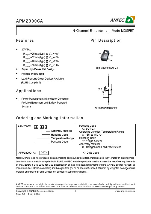
APM2300C A : C00X
X - Date Code
Note: ANPEC lead-free products contain molding compounds/die attach materials and 100% matte tin plate termination finish; which are fully compliant with RoHS. ANPEC lead-free products meet or exceed the lead-free requirements of IPC/JEDEC J-STD-020C for MSL classification at lead-free peak reflow temperature. ANPEC defines “Green” to mean lead-free (RoHS compliant) and halogen free (Br or Cl does not exceed 900ppm by weight in homogeneous material and total of Br and Cl does not exceed 1500ppm by weight).
2
1
Duty = 0.5
0.2
0.1
0.1
0.05
0.02
0.01
0.01 Single Pulse
1E-3 1E-4 1E-3 0.01 0.1
Mounted on 1in2 pad R : 150 oC/W
θJA
1 10 100
Square Wave Pulse Duration (sec)
APM2301中文资料
ANPEC reserves the right to make changes to improve reliability or manufacturability without notice, and advise customers to obtain the latest version of relevant information to verify before placing orders.Pin DescriptionOrdering and Marking InformationFeaturesApplicationsAbsolute Maximum Ratings (T A = 25°C unless otherwise noted)• -20V/-2.8A , R DS(ON)=72m Ω(typ.) @ V GS =-10VR DS(ON)=100m Ω(typ.) @ V GS =-4.5V• Super High Dense Cell Design for ExtremelyLow R DS(ON)• Reliable and Rugged • SOT-23 Package• Power Management in Notebook Computer ,Portable Equipment and Battery Powered Systems.* Surface Mounted on FR4 Board, t ≤ 10 sec.G DSTop View of SOT-23Notesa : Pulse test ; pulse width ≤300µs, duty cycle ≤ 2%b: Guaranteed by design, not subject to production testingAbsolute Maximum Ratings Cont. (T A = 25°C unless otherwise noted)Electrical Characteristics (T A = 25°C unless otherwise noted)2468100.0300.0450.0600.0750.0900.1050.1200.1350.150012345246810-50-2502550751001251500.000.250.500.751.001.251.500.00.5 1.0 1.5 2.0 2.50246810Typical Characteristics-I D -D r a i n C u r r e n t (A )Transfer Characteristics-V GS - Gate-to-Source Voltage (V)Threshold Voltage vs. Junction T emperatureTj - Junction T emperature (°C)-V G S (t h )-T h r e s h o l d V o l t a g e (V )(N o r m a l i z e d )R D S (O N )-O n -R e s i s t a n c e (Ω)On-Resistance vs. Drain Current-I D - Drain Current (A)Output Characteristics-I D -D r a i n C u r r e n t (A )-V DS - Drain-to-Source Voltage (V)369121505101520-50-25025507510012515012345678910Typical CharacteristicsR D S (O N )-O n -R e s i s t a n c e (Ω)(N o r m a l i z e d )On-Resistance vs. Junction TemperatureT J - Junction Temperature (°C)-V DS - Drain-to-Source Voltage (V)CapacitanceC a p a c i t a n c e (p F )-V GS - Gate-to-Source Voltage (V)R D S (O N )-O n -R e s i s t a n c e (Ω)On-Resistance vs. Gate-to-Source VoltageGate ChargeQ G - Gate Charge (nC)-V G S -G a t e -S o u r c e V o l t a g e (V )0.00.20.40.60.8 1.0 1.2 1.4 1.61100.010.1110100024681012141E-41E-30.010.11101000.010.11Typical CharacteristicsP o w e r (W )Single Pulse PowerTime (sec)Square Wave Pulse Duration (sec)Source-Drain Diode Forward Voltage-I S -S o u r c e C u r r e n t (A )-V SD -Source-to-Drain Voltage (V)N o r m a l i z e d E f f e c t i v e T r a n s i e n t T h e r m a l I m p e d a n c eNormalized Thermal Transient Impedence, Junction to AmbientPackaging Information SOT-23Physical SpecificationsReflow Condition (IR/Convection or VPR Reflow)Reference JEDEC Standard J-STD-020A APRIL 1999Classification Reflow ProfilesPackage Reflow ConditionsPre-heat temperature183 CPeak temperatureTime°t e m p e r a t u r eReliability test programCarrier Tape & Reel DimensionsCover Tape DimensionsCustomer ServiceAnpec Electronics Corp.Head Office :5F, No. 2 Li-Hsin Road, SBIP,Hsin-Chu, T aiwan, R.O.C.T el : 886-3-5642000Fax : 886-3-5642050Taipei Branch :7F, No. 137, Lane 235, Pac Chiao Rd.,Hsin Tien City, Taipei Hsien, T aiwan, R. O. C.T el : 886-2-89191368Fax : 886-2-89191369。
AM2301

温湿度模块AM2301 产品手册更多详情请登陆:一、产品概述AM2301湿敏电容数字温湿度模块是一款含有己校准数字信号输出的温湿度复合传感器。
它应用专用的数字模块采集技术和温湿度传感技术,确保产品具有极高的可靠性与卓越的长期稳定性。
传感器包括一个电容式感湿元件和一个高精度测温元件,并与一个高性能8位单片机相连接。
因此该产品具有品质卓越、超快响应、抗干扰能力强、性价比极高等优点。
每个传感器都在极为精确的湿度校验室中进行校准。
校准系数以程序的形式储存在单片机中,传感器内部在检测信号的处理过程中要调用这些校准系数。
标准单总线接口,使系统集成变得简易快捷。
超小的体积、极低的功耗,信号传输距离可达20米以上,使其成为各类应用甚至最为苛刻的应用场合的最佳选择。
产品为3引线(单总线接口)连接方便。
特殊封装形式可根据用户需求而提供。
实物图外形尺寸(单位:mm)二、应用范围暖通空调、除湿器、测试及检测设备、消费品、汽车、自动控制、数据记录器、家电、湿度调节器、医疗、气象站、及其他相关湿度检测控制等。
三、产品亮点超低能耗、传输距离远、全部自动化校准、采用电容式湿敏元件、完全互换、标准数字单总线输出、卓越的长期稳定性、采用高精度测温元件。
四、单总线接口定义4.1 AM2301引脚分配表1:AM2301引脚分配图1:AM2301引脚分配图4.2 电源引脚(VDD GND)AM2301的供电电压范围为3.3V - 5.2V,建议供电电压为5V。
4.3 串行数据(SDA)SDA引脚为三态结构,用于读、写传感器数据。
具体的通信时序,见通信协议的详细说明。
五、传感器性能 5.1 相对湿度表2: AM2301相对湿度性能表图2: 25℃时AM2301的相对湿度最大误差 图3:温度传感器的温度最大误差六、电气特性电气特性,如能耗,高、低电平,输入、输出电压等,都取决于电源。
表4详细说明了AM2301的电气特性,若没有标明,则表示供电电压为5V 。
APM使用Copter(直升机和多轴)固件的中文参数表

10
米
1 -- 127
circle繞圈模式時的繞圈半徑
CIRCLE_RATE
20
度/秒
-90 -- 90
circle繞圈模式時的繞圈角速度
COMPASS-AUTODEC
1
0,1
自動磁偏角開關,0關閉,1開啟
COMPASS_DEC
-0.083
度
磁偏角設置,請根據本地磁偏角輸入,具體可登入/查詢
電池資訊顯示開關,0-不顯示;3-只顯示電壓;4-顯示電流和電壓
BATT_VOLT_MULT
10.1
設置電壓感測器埠採集的電壓與實際電壓的倍數,如:電壓檢測PIN腳測出來2V,那麼實際電壓應該是2X10.1=20.2V
BATT_VOLT_PIN
13
-1,0,1,2,13,100
設置電壓感測器使用的埠,-1不使用;0-A0;1—A1;2- Pixhawk用;13-A13;100-PX4用
快門觸發設置,如果不為零將根據GPS的移動距離進行拍照,例如:設置5米,那麼將根據GPS定位資訊,每飛行5秒就按一次快門
CAM_TRIGG_TYPE
0
0,1
快門觸發類型設置,0-舵機,1-繼電器
CH7_OPT
0
通道7操作設置(PWM值1800以上),0:無, 2:Flip, 3:簡單模式, 4:返航, 5:Save Trim, 7:Save WP, 8:Multi Mode, 9:Camera Trigger, 10:開聲納, 11:Fence, 12:ResetToArmedYaw, 13:Super Simple Mode, 14:Acro Trainer, 16:自動, 17:自動調參
SPP2301A P-Channel Enhancement Mode MOSFET 说明书

现货库存、技术资料、百科信息、热点资讯,精彩尽在鼎好!SPP2301AP-Channel Enhancement Mode MOSFET DESCRIPTION APPLICATIONSThe SPP2301A is the P-Channel logic enhancementmode power field effect transistors are produced using high cell density , DMOS trench technology.This high density process is especially tailored to minimize on-state resistance.These devices are particularly suited for low voltage application such as cellular phone and notebook computer power management and other battery powered circuits, and low in-line power loss are needed in a very small outline surface mount package.z Power Management in Note book z Portable Equipmentz Battery Powered System z DC/DC Converterz Load Switchz DSCz LCD Display inverter FEATURES PIN CONFIGURATION(SOT-23-3L)PART MARKING-20V/-2.8A,R DS(ON)=150m Ω@V GS =-4.5V-20V/-2.0A,R DS(ON)=275m Ω@V GS =-2.5VSuper high density cell design for extremely lowR DS (ON)Exceptional on-resistance and maximum DCcurrent capabilitySOT-23-3L package designTYPICAL CHARACTERISTICSTYPICAL CHARACTERISTICSTYPICAL CHARACTERISTICSInformation provided is alleged to be exact and consistent. SYNC Power Corporation presumes no responsibility for the penalties of use of such information or for any violation of patents or other rights of third parties which may result from its use. No license is granted by allegation or otherwise under any patent or patent rights of SYNC Power Corporation. Conditions mentioned in this publication are subject to change without notice. This publication surpasses and replaces all information previously supplied. SYNC Power Corporation products are not authorized for use as critical components in life support devices or systems without express written approval of SYNC Power Corporation.©The SYNC Power logo is a registered trademark of SYNC Power Corporation©2004 SYNC Power Corporation – Printed in Taiwan – All Rights ReservedSYNC Power Corporation9F-5, No.3-2, Park StreetNanKang District (NKSP), Taipei, Taiwan, 115, R.O.CPhone: 886-2-2655-8178Fax: 886-2-2655-8468©。
ADP2300_2301_cn开关电源中文版
65 60
0 0.2 0.4 0.6 IOUT (A) 0.8
VIN = 12V VOUT = 5.0V 1.0 1.2
08342-069
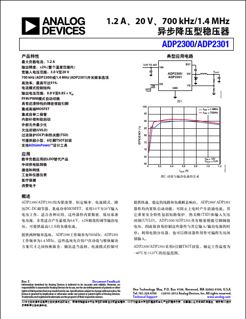
图2. 功效与输出电流的关系
概述
ADP2300/ADP2301均为紧凑型、恒定频率、电流模式、降 压DC-DC调节器,集成功率MOSFET,采用3.0 V至20 V输入 电压工作,适合各种应用。这些器件内置精密、低压基准 电压源,非常适合产生最低为0.8 V、±2%精度的调节输出电 压,可提供最高1.2 A的负载电流。 提供两种频率选项: ADP2300工作频率为700 kHz,ADP2301 工作频率为1.4 MHz。这些选项允许用户在功效与整体解决 方案尺寸之间权衡取舍,做出适当选择。电流模式控制可 提供快速、稳定的线路和负载瞬态响应。 ADP2300/ ADP2301 器件均内置软启动功能,可防止上电时产生浪涌电流。其 它重要安全特性包括短路保护、热关断 (TSD)和输入欠压 闭锁 (UVLO)。 ADP2300/ADP2301具有精密使能引脚阈值 电压,因此很容易控制这些器件与其它输入/输出电源的时 序;利用电阻分压器,也可以将该器件用作可编程欠压闭 锁输入。 ADP2300/ADP2301采用6引脚TSOT封装,额定工作温度为 −40°C至+125°C的结温范围。
ADI中文版数据手册是英文版数据手册的译文,敬请谅解翻译中可能存在的语言组织或翻译错误,ADI不对翻译中存在的差异或由此产生的错误负责。如需确认任何词语的准确性,请参考ADI提供 的最新英文版数据手册。
ADP2300/ADP2301
目录
特性 ..............................................................................
APM2300AA中文资料

ANPEC reserves the right to make changes to improve reliability or manufacturability without notice, and advise customers to obtain the latest version of relevant information to verify before placing orders.APM2300AAFeaturesApplications• Power Management in Notebook Computer ,Portable Equipment and Battery Powered Systems.Pin DescriptionOrdering and Marking InformationAPM2300AHandling Code Tem p. Range Package CodePackage Code A : SOT-23Operating Junction Tem p. Range C : -55 to 150°C Handling CodeTU : Tube TR : Tape & Reel Lead Free CodeL : Lead Free Device Blank : Original Device APM2300A A :A00XXXXXX - Date CodeLead Free Code T op View of SOT-23N-Channel MOSFET• 20V/6A ,R DS(ON)=25m Ω(typ.) @ V GS =10V R DS(ON)=32m Ω(typ.) @ V GS =4.5V R DS(ON)=40m Ω(typ.) @ V GS =2.5V• Super High Dense Cell Design • Reliable and Rugged•Lead Free Available (RoHS Compliant)DGSGNote: ANPEC lead-free products contain molding compounds/die attach materials and 100% matte in plate termina-tion finish; which are fully compliant with RoHS and compatible with both SnPb and lead-free soldiering operations.ANPEC lead-free products meet or exceed the lead-free requirements of IPC/JEDEC J STD-020C for MSL classifica-tion at lead-free peak reflow temperature.APM2300AAAbsolute Maximum Ratings (T A = 25°C unless otherwise noted)*Surface Mounted on 1in2 pad area, t ≤ 10sec.Electrical Characteristics (T A = 25°C unless otherwise noted)APM2300AAElectrical Characteristics (Cont.) (T A = 25°C unless otherwise noted)a : Pulse test ; pulse width≤300µs, duty cycle≤2%.b : Guaranteed by design, not subject to production testing.APM2300AA1E-41E-30.010.11101001E-30.010.112Typical CharacteristicsI D - D r a i n C u r r e n t (A )Drain CurrentT j - Junction Temperature (°C)Safe Operation AreaV DS - Drain - Source Voltage (V)N o r m a l i z e d T r a n s i e n t T h e r m a l R e s i s t a n c eThermal Transient ImpedanceSquare Wave Pulse Duration (sec)Power DissipationP t o t - P o w e r (W )T j - Junction T emperature (°C)I D - D r a i n C u r r e n t (A )204060801001201401600.00.10.20.30.40.50.60.70.80.91.020406080100120140160012345670.11101000.010.1110100APM2300AADrain-Source On Resistance I D - Drain Current (A)T j - Junction T emperature (°C)Gate Threshold VoltageV DS - Drain - Source Voltage (V)I D - D r a i n C u r r e n t (A )Output Characteristics Transfer CharacteristicsV GS - Gate - Source Voltage (V)I D - D r a i n C u r r e n t(A )N o r m a l i z e d T h r e s h o l d V o l ta g eTypical Characteristics (Cont.)246810024681012141618204812162002468101214161820-50-2502550751001251500.000.250.500.751.001.251.50APM2300AAV DS - Drain - Source Voltage (V)Drain-Source On ResistanceN o r m a l i z e d O n R e s i s t a n c eT j - Junction T emperature (°C)C - C a p a c i t a n c e (p F )I S - S o u r c e C u r r e n t (A )CapacitanceQ G - Gate Charge (nC)V G S - G a t e - s o u r c e V o l t a g e (V )Typical Characteristics (Cont.)-50-252550751001251500.00.20.40.60.81.01.21.41.61.82.0110200160320480640800012345612345APM2300AA Packaging Information SOT-23APM2300AAT LT P25T e m p e r a t u r eTim eReflow Condition (IR/Convection or VPR Reflow)Classification Reflow ProfilesPhysical SpecificationsAPM2300AAClassification Reflow Profiles(Cont.)Reliability Test ProgramCarrier Tape & Reel DimensionsAPM2300AACarrier Tape & Reel Dimensions(Cont.)(mm) Cover Tape DimensionsCustomer ServiceAnpec Electronics Corp.Head Office :5F, No. 2 Li-Hsin Road, SBIP,Hsin-Chu, T aiwan, R.O.C.T el : 886-3-5642000Fax : 886-3-5642050Taipei Branch :7F, No. 137, Lane 235, Pac Chiao Rd.,Hsin Tien City, Taipei Hsien, T aiwan, R. O. C.T el : 886-2-89191368Fax : 886-2-89191369。
- 1、下载文档前请自行甄别文档内容的完整性,平台不提供额外的编辑、内容补充、找答案等附加服务。
- 2、"仅部分预览"的文档,不可在线预览部分如存在完整性等问题,可反馈申请退款(可完整预览的文档不适用该条件!)。
- 3、如文档侵犯您的权益,请联系客服反馈,我们会尽快为您处理(人工客服工作时间:9:00-18:30)。
APM2301CA
ANPEC reserves the right to make changes to improve reliability or manufacturability without notice, and advise
customers to obtain the latest version of relevant information to verify before placing orders.Pin Description
Ordering and Marking Information
Features
Applications
•
-20V/-2.8A
R DS(ON)= 56m Ω (typ.) @ V GS = -4.5V R DS(ON)= 85m Ω (typ.) @ V GS = -2.5V R DS(ON)= 106m Ω (typ.) @ V GS = -1.8V
•Super High Dense Cell Design •
Reliable and Rugged
APM2301CA
Handling Code Temp. Range Package Code
Package Code A : SOT-23
Operating Junction Temp. Range
C : -55 to 150 C
Handling Code TR : Tape & Reel Lead Free Code
L : Lead Free Device Blank : Original Device APM2301CA:C01X
XXXXX - Date Code
Lead Free Code Note: ANPEC lead-free products contain molding compounds/die attach materials and 100% matte tin plate termination finish; which are fully compliant with RoHS and compatible with both SnPb and lead-free soldiering operations. ANPEC lead-free products meet or exceed the lead-free requirements of IPC/JEDEC J STD-020C for MSL classification at lead-free peak reflow temperature.
°•
Power Management in Notebook Computer,
Portable Equipment and Battery Powered Systems.
P Channel MOSFET
SOT-23
G
S
APM2301CA
Absolute Maximum Ratings (T A = 25°C Unless Otherwise Noted)
Electrical Characteristics (T A = 25°C Unless Otherwise Noted)
Notes: *Surface Mounted on 1in 2
pad area, t ≤ 10sec.
APM2301CA
Electrical Characteristics (Cont.) (T
= 25°C Unless Otherwise Noted)
A
Notes:
a : Pulse test ; pulse width≤300µs, duty cycle≤2%.
b : Guaranteed by design, not subject to production testing.
APM2301CA
Typical Characteristics
-I D - D r a i n C u r r e n t (A )
Drain Current
T j - Junction Temperature (°C)
Safe Operation Area
-V DS - Drain - Source Voltage (V)Thermal Transient Impedance
Square Wave Pulse Duration (sec)
Power Dissipation
P t o t - P o w e r (W )
T j - Junction Temperature (°C)
-I D - D r a i n C u r r e n t (A )
N o r m a l i z e d E
f f e c t i v e T r a n s i e n t 0
20
40
60
80100120140160
0.0
0.10.20.30.40.5
0.60.7
0.80.91.0
0.0
0.5
1.0
1.5
2.0
2.5
3.0
0.01
0.11
10100
0.010.1
1
10
50
1E-30.01
0.1
1
2
-50-250255075100125150 -V GS - Gate - Source Voltage (V)
T j - Junction Temperature (°C)
APM2301CA
-V DS - Drain - Source Voltage (V)
Drain-Source On Resistance
N o r m a l i z e d O n R e s i s t a n c e
T j - Junction Temperature (°C)
C - C a p a c i t a n c e (n C )
-I S - S o u r c e C u r r e n t (A )
Capacitance
Q G - Gate Charge (nC)
-V G S - G a t e - S o u r c e V o l t a g e (V )
Typical Characteristics (Cont.)
-50-25
25
50
75100125150
0.2
0.40.60.81.01.21.41.6
1.8
2.0
0.11
10
0100200300400500600
700
800
1
2
3
4
5
6
7
0.00.51.01.52.02.53.03.54.04.5
APM2301CA
Packaging Information SOT-23
Physical Specifications
APM2301CA
Reflow Condition
(IR/Convection or VPR Reflow)
T L
T P
25
T e m p e r a t u r e
Reflow Condition
Notes: All temperatures refer to topside of the package .Measured on the body surface.
APM2301CA
Reflow Condition
Reliability test program
Carrier Tape & Reel Dimensions
APM2301CA
Carrier Tape & Reel Dimensions (Cont.)
Cover Tape Dimensions
Customer Service
Anpec Electronics Corp.
Head Office :
No.6, Dusing 1st Road, SBIP,
Hsin-Chu, Taiwan, R.O.C.
Tel : 886-3-5642000
Fax : 886-3-5642050
Taipei Branch :
7F, No. 137, Lane 235, Pac Chiao Rd.,
Hsin Tien City, Taipei Hsien, Taiwan, R. O. C.
Tel : 886-2-89191368
Fax : 886-2-89191369。