tps63002
用全集成降-升压转换器延长锂离子电池寿命的设计

用全集成降/升压转换器延长锂离子电池寿命的设计引言 对于便携式电源应用而言,要充分利用先进电池技术的小尺寸、高能量密度等优点,就必须在整个电池放电电压范围内实现高效工作。
这就对要求3.3V总线电压的锂离子电池供电系统提出了严峻的挑战。
尽管标准降压转换器在将4.2~3.0V锂离子电池电压转换成诸如1.8V的较低输出电压时具有很高的转换效率,且标准升压转换器在将锂离子电池电压转换成诸如5V的更高输出电压时也有很高的转换效率,但上述两种转换器均不是生成常用3.3V总线电压的最佳解决方案。
SEPIC及传统的降压-升压虽然能够充分利用电池电量,但却具有效率低、成本高、电路板面积较大及部件数量多等缺点。
采用三种配置结构的TPS6300x可以解决这些问题。
TPS63000具有从1.2V~5.5V的可调输出范围。
TPS63001及TPS63002的固定输出电压分别为3.3V和5.0V。
上述产品均采用节省空间的10引脚QFN(DRC)封装。
TPS63001 TI的TPS63001具有部件数最少、电路板面积小、成本较低等特点,且能够将锂离子电池输入电压高效地转换为3.3V总线电压。
在一个3x3毫米QFN封装中除集成了降压和升压两种功能以外,还集成了开关FET、补偿和保护功能等。
只需三个外部部件即可保证工作运行:输入和输出电容以及电感。
该转换器的峰值效率为96%(请参见TPS6300x基于如当锂离子电池放电至并低于3.3V时,降压-升压转换器必须要从降压模式转换为升压模式。
在该转换点,许多降压-升压控制机制会出现效率下降、电源抖动或输出电压不稳的情况。
TPS6300x可根据需要在降压和升压模式间以逐脉冲方式进行无缝转换,因而能够在降压和升压范围内提供恒定的PWM开关,而不会在两个模式间产生迭。
艾德克斯IT6302 用户手册

三路可编程直流电源供应器
IT6302 用户手册
型号:IT6302 版本号:V3.1
声明
© Itech Electronics, Co., Ltd. 2014 根据国际版权法, 未经 Itech Electronics, Co., Ltd. 事先允许和书面同意, 不得以任 何形式(包括电子存储和检索或翻译为其 他国家或地区语言)复制本手册中的任何 内容。
安全注意事项
在此仪器操作的各个阶段中,必须遵循以下一般安全预防措施。如果未遵循这些 预防措施或本手册其他部分说明的特定警告,则会违反有关仪器的设计、制造和 用途方面的安全标准。 艾德克斯公司对用户不遵守这些预防措施的行为不承担任 何责任。 请勿使用已损坏的设备。在使用设备之前,请先检查其外壳。检查是否存在 裂缝。请勿在含有易爆气体、蒸汽或粉尘的环境中操作本设备。 电源出厂时提供了一个三芯电源线,您的电源供应器应该被连接到三芯的接 线盒上。在操作电源供应器之前,您应首先确定电源供应器接地良好! 请始终使用所提供的电缆连接设备。 在连接设备之前,请观察设备上的所有标记。 使用具有适当额定负载的电线,所有负载电线的容量必须能够承受电源的最 大短路输出电流而不会发生过热。如果有多个负载,则每对负载电线都必须 能安全承载电源的满载额定短路输出电流。 为减少起火和电击风险,请确保市电电源的电压波动不超过工作电压范围的 10%。 如果用电源给电池充电, 在接线时要注意电池的正负极性, 否则会烧坏电源! 请勿自行在仪器上安装替代零件,或执行任何未经授权的修改。 请勿在可拆卸的封盖被拆除或松动的情况下使用本设备。 请仅使用制造商提供的电源适配器以避免发生意外伤害。 严禁将本设备使用于生命维持系统或其他任何有安全要求的设备上。
icap6300技术参数
icap6300技术参数ICAP6300是一款先进的集成电路分析仪,具有出色的性能和功能。
本文将从技术参数的角度来介绍ICAP6300的特点和优势。
ICAP6300的频率范围非常广泛,可覆盖从直流到40 GHz的频率范围。
这使得它在各种应用场景下都能够满足需求,无论是通信、雷达、卫星通信还是无线电等领域,ICAP6300都可以提供精确的测量结果。
ICAP6300具有出色的动态范围。
动态范围是衡量仪器测量能力的重要指标,它表示仪器在测量过程中能够处理的最大和最小功率之间的差异。
ICAP6300的动态范围可达到70 dB,这意味着它能够准确地测量强信号和弱信号,保证了测量结果的准确性和可靠性。
ICAP6300还具有高精度的测量能力。
它的测量精度可以达到0.1 dB,这意味着它能够准确地测量信号的功率和频率。
它还能够在不同的测量模式下进行高速测量,提高了测量效率和生产效率。
ICAP6300还具有多种测量模式和功能。
它支持功率、频率、相位、谐波等多种测量参数的测量,能够满足不同应用场景的需求。
此外,它还支持多种接口,如USB、LAN和GPIB等,方便与其他设备进行连接和数据传输。
除了以上的技术参数外,ICAP6300还具有人性化的操作界面和强大的数据处理能力。
它采用了直观的图形界面,使得操作更加简单和方便。
同时,它还配备了强大的数据处理软件,可以对测量数据进行分析、处理和存储,为用户提供全面的数据支持。
ICAP6300作为一款先进的集成电路分析仪,具有广泛的频率范围、出色的动态范围、高精度的测量能力和多种测量模式和功能。
它的性能和功能使得它在各个领域都有广泛的应用,为用户提供准确、可靠的测量结果。
无论是在通信、雷达、卫星通信还是无线电等领域,ICAP6300都是一款值得信赖的仪器。
基于WSN的农业大棚智能环境监控系统研究

第15期2019年8月No.15 August,2019作者简介:秦芹(1984— ),女,河北沧州人,讲师,硕士;研究方向:计算机控制。
摘 要:文章研究了基于WSN 的农业大棚环境监控系统,分别从环境监控系统的硬件设计、软件设计以及系统优化几个方面进行了分析和研究。
以保定地区草莓种植基地作为测试环境,对本系统进行了为期3个月的测试。
实验结果表明,本系统能够实时、准确地采集环境信息。
关键词:智能环境监控;无线传感器网络;农业大棚基于WSN的农业大棚智能环境监控系统研究秦 芹(保定学院,河北 保定 071000)近几年,随着物联网技术的发展,无线传感器网络(Wireless Sensor Networks ,WSN )也在各行各业得到应用。
草莓种植一直是保定地区农业方面的主要产业之一,目前,草莓种植基地的温室环境还没有实现智能化监控及管理,这也是草莓产量不能有大幅增长的原因之一。
因此,本文将WSN 应用到地区草莓种植基地的温室环境监控系统中,实现温室环境的智能化监控及管理[1-3]。
1 系统原理及方法WSN 是由传感器模块、处理器模块、无线通信模块和能量供应模块组成的大量传感器节点,多个传感器节点组成分布式网络。
本系统采用CC2530作为传感器节点的处理器模块,主要负责传感器节点的数据存储、处理和多任务处理。
传感器选择温度、湿度、光照、二氧化碳质量浓度等传感器,主要负责温室信息的采集和数据转换。
无线通信模块采用ZigBee 技术,具有功耗低、数据传输可靠、兼容性好、实现成本低以及组网方便的优点,非常适合低速率传输的无线传感器网络[4-5],主要负责组网、数据传递和指令交换等。
2 系统硬件设计2.1 系统整体设计传感器节点采集数据信息后,通过ZigBee 技术将数据信息传递给协调器。
协调器将收集到的数据信息通过串口传递到上位机,并在上位机界面显示。
上位机实现了信息实时显示、查询历史数据、设置阈值、远程控制各种设备等功能,具体系统结构如图1所示。
itech6332a参数

iTech6332a参数1. 简介iTech6332a参数是一种用于描述和配置iTech6332a设备的参数。
iTech6332a是一款先进的技术设备,广泛应用于各个行业和领域。
通过合理地配置参数,可以使iTech6332a设备发挥最佳性能,提高工作效率和质量。
2. 参数列表下面是iTech6332a设备的常见参数列表:•型号: iTech6332a•尺寸: 根据不同型号而异•重量: 根据不同型号而异•电压: 根据不同型号而异•功率: 根据不同型号而异•工作温度范围: 根据不同型号而异•存储温度范围: 根据不同型号而异•通信接口: USB、以太网等•输入电流范围•输出电流范围•精度•频率范围•波形类型•特殊功能3. 参数详解3.1 型号iTech6332a有多个型号可供选择,每个型号在功能和性能上有所差异。
用户可以根据自己的需求选择合适的型号。
3.2 尺寸iTech6332a的尺寸根据不同型号而异,通常会在产品说明书中提供详细的尺寸参数。
用户在使用时需要考虑设备的大小是否适合自己的工作环境。
3.3 重量iTech6332a的重量也根据不同型号而异,重量参数通常会影响设备的便携性和稳定性。
用户在选择设备时需要根据实际需求进行权衡。
3.4 电压iTech6332a设备的电压是指输入电压范围,用户需要根据实际情况选择合适的电压范围,以确保设备能够正常工作。
3.5 功率iTech6332a设备的功率是指设备能够提供的最大功率输出。
用户在选择设备时需要考虑所需功率是否满足自己的工作需求。
3.6 工作温度范围iTech6332a设备的工作温度范围是指设备可以正常工作的环境温度范围。
用户在使用时需要确保工作环境温度不超出该范围,以免影响设备性能和寿命。
3.7 存储温度范围iTech6332a设备的存储温度范围是指设备可以安全存储的环境温度范围。
用户在长时间不使用设备时需要将其存储在符合要求的环境中,以保证设备质量和寿命。
tps63020评估手册

IMPORTANT NOTICETexas Instruments Incorporated and its subsidiaries (TI) reserve the right to make corrections, modifications, enhancements, improvements, and other changes to its products and services at any time and to discontinue any product or service without notice. Customers should obtain the latest relevant information before placing orders and should verify that such information is current and complete. All products are sold subject to TI’s terms and conditions of sale supplied at the time of order acknowledgment.TI warrants performance of its hardware products to the specifications applicable at the time of sale in accordance with TI’s standard warranty. T esting and other quality control techniques are used to the extent TI deems necessary to support this warranty. Except where mandated by government requirements, testing of all parameters of each product is not necessarily performed.TI assumes no liability for applications assistance or customer product design. Customers are responsible for their products and applications using TI components. T o minimize the risks associated with customer products and applications, customers should provide adequate design and operating safeguards.TI does not warrant or represent that any license, either express or implied, is granted under any TI patent right, copyright, mask work right, or other TI intellectual property right relating to any combination, machine, or process in which TI products or services are used. Information published by TI regarding third-party products or services does not constitute a license from TI to use such products or services or a warranty or endorsement thereof. Use of such information may require a license from a third party under the patents or other intellectual property of the third party, or a license from TI under the patents or other intellectual property of TI.Reproduction of information in TI data books or data sheets is permissible only if reproduction is without alteration and is accompanied by all associated warranties, conditions, limitations, and notices. Reproduction of this information with alteration is an unfair and deceptive business practice. TI is not responsible or liable for such altered documentation.Resale of TI products or services with statements different from or beyond the parameters stated by TI for that product or service voids all express and any implied warranties for the associated TI product or service and is an unfair and deceptive business practice. TI is not responsible or liable for any such statements. Following are URLs where you can obtain information on other Texas Instruments products and application solutions:Products ApplicationsAmplifiers Audio /audioData Converters Automotive /automotiveDSP Broadband /broadbandInterface Digital Control /digitalcontrolLogic Military /militaryPower Mgmt Optical Networking /opticalnetwork Microcontrollers Security /securityTelephony /telephonyVideo & Imaging /videoWireless /wirelessMailing Address:Texas InstrumentsPost Office Box 655303 Dallas, Texas 75265Copyright 2004, Texas Instruments IncorporatedEVM IMPORTANT NOTICETexas Instruments (TI) provides the enclosed product(s) under the following conditions:This evaluation kit being sold by TI is intended for use for ENGINEERING DEVELOPMENT OR EVALUATION PURPOSES ONLY and is not considered by TI to be fit for commercial use. As such, the goods being provided may not be complete in terms of required design-, marketing-, and/or manufacturing-related protective considerations, including product safety measures typically found in the end product incorporating the goods. As a prototype, this product does not fall within the scope of the European Union directive on electromagnetic compatibility and therefore may not meet the technical requirements of the directive.Should this evaluation kit not meet the specifications indicated in the EVM User’s Guide, the kit may be returned within 30 days from the date of delivery for a full refund. THE FOREGOING WARRANTY IS THE EXCLUSIVE WARRANTY MADE BY SELLER TO BUYER AND IS IN LIEU OF ALL OTHER WARRANTIES, EXPRESSED, IMPLIED, OR STATUTORY, INCLUDING ANY WARRANTY OF MERCHANTABILITY OR FITNESS FOR ANY PARTICULAR PURPOSE.The user assumes all responsibility and liability for proper and safe handling of the goods. Further, the user indemnifies TI from all claims arising from the handling or use of the goods. Please be aware that the products received may not be regulatory compliant or agency certified (FCC, UL, CE, etc.). Due to the open construction of the product, it is the user’s responsibility to take any and all appropriate precautions with regard to electrostatic discharge.EXCEPT TO THE EXTENT OF THE INDEMNITY SET FORTH ABOVE, NEITHER PARTY SHALL BE LIABLE TO THE OTHER FOR ANY INDIRECT, SPECIAL, INCIDENTAL, OR CONSEQUENTIAL DAMAGES.TI currently deals with a variety of customers for products, and therefore our arrangement with the user is not exclusive.TI assumes no liability for applications assistance, customer product design, software performance, or infringement of patents or services described herein.Please read the EVM User’s Guide and, specifically, the EVM Warnings and Restrictions notice in the EVM User’s Guide prior to handling the product. This notice contains important safety information about temperatures and voltages. For further safety concerns, please contact the TI application engineer.Persons handling the product must have electronics training and observe good laboratory practice standards. No license is granted under any patent right or other intellectual property right of TI covering or relating to any machine, process, or combination in which such TI products or services might be or are used.Mailing Address:Texas InstrumentsPost Office Box 655303Dallas, Texas 75265Copyright 2004, Texas Instruments IncorporatedEVM WARNINGS AND RESTRICTIONSIt is important to operate this EVM within the input voltage range of 0 V and 7 V.Exceeding the specified input range may cause unexpected operation and/or irreversible damage to the EVM. If there are questions concerning the input range, please contact a TI field representative prior to connecting the input power.Applying loads outside of the specified output range may result in unintended operation and/or possible permanent damage to the EVM. Please consult the EVM User’s Guide prior to connecting any load to the EVM output. If there is uncertainty as to the load specification, please contact a TI field representative.During normal operation, some circuit components may have case temperatures greater than +25°C. The EVM is designed to operate properly with certain components above +25°C as long as the input and output ranges are maintained. These components include but are not limited to linear regulators, switching transistors, pass transistors, and current sense resistors. These types of devices can be identified using the EVM schematic located in the EVM User’s Guide. When placing measurement probes near these devices during operation, please be aware that these devices may be very warm to the touch.Mailing Address:Texas InstrumentsPost Office Box 655303Dallas, Texas 75265Copyright 2004, Texas Instruments Incorporated。
敦泰触摸IC参数对照表
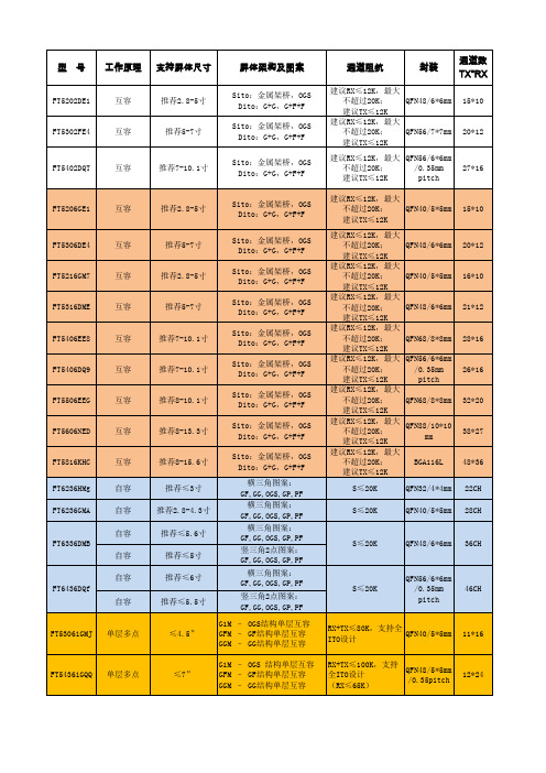
20*12
FT5402DQT
互容
推荐7-10.1寸
27*16
FT5206GE1
互容
推荐2.8-5寸
Sito:金属架桥,OGS Dito:G+G,G+F+F Sito:金属架桥,OGS Dito:G+G,G+F+F Sito:金属架桥,OGS Dito:G+G,G+F+F Sito:金属架桥,OGS Dito:G+G,G+F+F Sito:金属架桥,OGS Dito:G+G,G+F+F Sito:金属架桥,OGS Dito:G+G,G+F+F Sito:金属架桥,OGS Dito:G+G,G+F+F Sito:金属架桥,OGS Dito:G+G,G+F+F Sito:金属架桥,OGS Dito:G+G,G+F+F 横三角图案: GF,GG,OGS,GP,PF 横三角图案: GF,GG,OGS,GP,PF 横三角图案: GF,GG,OGS,GP,PF 竖三角2点图案: GF,GG,OGS,GP,PF 横三角图案: GF,GG,OGS,GP,PF 竖三角2点图案: GF,GG,OGS,GP,PF G1M – OGS结构单层互容 GFM – GF结构单层互容 GGM – GG结构单层互容 G1M – OGS 结构单层互容 GFM – GF结构单层互容 GGM – GG结构单层互容
工作电流:6mA 待机电流:4mA 睡眠电流:30uA
工作温度: -20~+85 储存温度: -55~+150 工作温度: -20~+85 储存温度: -55~+150
基于STM32的瓦斯突出检测仪硬件电路设计

基于STM32的瓦斯突出检测仪硬件电路设计预测煤与瓦斯突出并将预测结果指标化已经成为开采煤与瓦斯突出煤层现场一项必不可少的工作。
是减少煤与瓦斯突出事故、实现煤矿安全生产的有效举措。
本文以应用研究为导向,设计了基于STM32的硬件电路,具有电路简单、测量准确等优点,可有效弥补现有仪器的不足。
近年来,我国煤矿瓦斯事故的发生频次仍然较高,国内外众多专家学者对煤矿瓦斯突出的预测指标一直进行着不懈的研究与探讨。
矿用瓦斯突出检测仪,是一种预测煤矿井下掘进工作面瓦斯突出危险性大小,能有效预测和防止瓦斯突出灾害的现代化电子设备。
它有利于作业人员实时掌握掘进工作面瓦斯突出的危险程度,在我国有着广泛的应用。
但是此类矿用瓦斯突出检测仪性能难以稳定,可靠性不高,测量数据不够准确,功耗也比较大,甚至在使用的过程中运送也不十分方便。
随着嵌入式系统和DSP技术的飞速发展,此类仪器的工作速度和智能化程度也有了较大的提升空间。
1 硬件电路设计1.1硬件系统框图矿用瓦斯突出检测仪,是一种典型的具备数据采集计算功能的嵌入式终端仪器。
其硬件组成如图1所示[1]。
图1 硬件系统框架图1.2嵌入式微处理器选择为达到低功耗、高可靠性、操作简便的目的,本设计采用选择意法半导体的144引脚的增强型处理器STM32103ZET6芯片为中央处理器。
该处理器采用32位Cortex-M3内核,片上系统时基(System Tick)能为轻量级操作系统的运行提供精准可控的硬件系统时钟,能灵活定制应用软件并运行轻量级操作系统[2]。
为更好地运行嵌入式系统的图形库,在芯片内部已有64K字节SRAM的基础上,又扩充了一片外部SRAM,以增加系统内存,具体电路如图2所示。
图2 外扩SRAM电路图1.3 数据存储单元为使系统具备存储采集数据和系统配置的能力,设计了SPI Flash存储器。
SPI Flash选用SST25VF064C,工作电压为3.3V,该存储芯片容量为8MB。