SN74LVC2G04YZPR中文资料
SN74LVC2G04DBVTE4中文资料

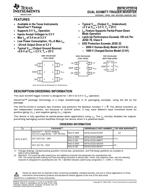
FEATURES1A 1Y2YGND2ADBV PACKAGE (TOP VIEW)YZP PACKAGE (BOTTOM VIEW)DCK PACKAGE (TOP VIEW)1A 1Y 2Y2A1A2A 1Y2Y GND DRL PACKAGE (TOP VIEW)See mechanical drawings for dimensions.V CC V CC CC V CC DESCRIPTION/ORDERING INFORMATIONSN74LVC2G04DUAL INVERTER GATESCES195L–APRIL 1999–REVISED JANUARY 2007•Available in the Texas Instruments •I off Supports Partial-Power-Down Mode NanoFree™PackageOperation•Supports 5-V V CC Operation •Latch-Up Performance Exceeds 100mA Per JESD 78,Class II•Inputs Accept Voltages to 5.5V •ESD Protection Exceeds JESD 22•Max t pd of 4.1ns at 3.3V–2000-V Human-Body Model (A114-A)•Low Power Consumption,10-µA Max I CC –200-V Machine Model (A115-A)•±24-mA Output Drive at 3.3V–1000-V Charged-Device Model (C101)•Typical V OLP (Output Ground Bounce)<0.8V at V CC =3.3V,T A =25°C•Typical V OHV (Output V OH Undershoot)>2V at V CC =3.3V,T A =25°CThis dual inverter is designed for 1.65-V to 5.5-V V CC operation.The SN74LVC2G04performs the Boolean function Y =A.NanoFree™package technology is a major breakthrough in IC packaging concepts,using the die as the package.This device is fully specified for partial-power-down applications using I off .The I off circuitry disables the outputs,preventing damaging current backflow through the device when it is powered down.ORDERING INFORMATIONT APACKAGE (1)ORDERABLE PART NUMBER TOP-SIDE MARKING (2)NanoFree™–WCSP (DSBGA)0.23-mm Large Bump –YZP Reel of 3000SN74LVC2G04YZPR ___CC_(Pb-free)Reel of 3000SN74LVC2G04DBVR SOT (SOT-23)–DBV C04_–40°C to 85°CReel of 250SN74LVC2G04DBVT Reel of 3000SN74LVC2G04DCKR SOT (SC-70)–DCK CC_Reel of 250SN74LVC2G04DCKT SOT (SOT-563)–DRLReel of 4000SN74LVC2G04DRLRCC_(1)Package drawings,standard packing quantities,thermal data,symbolization,and PCB design guidelines are available at /sc/package.(2)DBV/DCK/DRL:The actual top-side marking has one additional character that designates the assembly/test site.YZP:The actual top-side marking has three preceding characters to denote year,month,and sequence code,and one following character to designate the assembly/test site.Pin 1identifier indicates solder-bump composition (1=SnPb,•=Pb-free).Please be aware that an important notice concerning availability,standard warranty,and use in critical applications of Texas Instruments semiconductor products and disclaimers thereto appears at the end of this data sheet.1A1Y2A2YAbsolute Maximum Ratings(1)SN74LVC2G04DUAL INVERTER GATESCES195L–APRIL1999–REVISED JANUARY2007FUNCTION TABLE(EACH INVERTER)INPUT OUTPUTA YH LL HLOGIC DIAGRAM(POSITIVE LOGIC)over operating free-air temperature range(unless otherwise noted)MIN MAX UNIT V CC Supply voltage range–0.5 6.5VV I Input voltage range(2)–0.5 6.5VV O Voltage range applied to any output in the high-impedance or power-off state(2)–0.5 6.5VV O Voltage range applied to any output in the high or low state(2)(3)–0.5V CC+0.5VI IK Input clamp current V I<0–50mAI OK Output clamp current V O<0–50mAI O Continuous output current±50mAContinuous current through V CC or GND±100mADBV package165DCK package259θJA Package thermal impedance(4)°C/WDRL package142YZP package123T stg Storage temperature range–65150°C (1)Stresses beyond those listed under"absolute maximum ratings"may cause permanent damage to the device.These are stress ratingsonly,and functional operation of the device at these or any other conditions beyond those indicated under"recommended operating conditions"is not implied.Exposure to absolute-maximum-rated conditions for extended periods may affect device reliability.(2)The input negative-voltage and output voltage ratings may be exceeded if the input and output current ratings are observed.(3)The value of V CC is provided in the recommended operating conditions table.(4)The package thermal impedance is calculated in accordance with JESD51-7.Recommended Operating Conditions(1)SN74LVC2G04DUAL INVERTER GATESCES195L–APRIL1999–REVISED JANUARY2007MIN MAX UNIT Operating 1.65 5.5V CC Supply voltage VData retention only 1.5V CC=1.65V to1.95V0.65×V CCV CC=2.3V to2.7V 1.7V IH High-level input voltage VV CC=3V to3.6V2V CC=4.5V to5.5V0.7×V CCV CC=1.65V to1.95V0.35×V CCV CC=2.3V to2.7V0.7V IL Low-level input voltage VV CC=3V to3.6V0.8V CC=4.5V to5.5V0.3×V CCV I Input voltage0 5.5V V O Output voltage0V CC VV CC=1.65V–4V CC=2.3V–8I OH High-level output current–16mAV CC=3V–24V CC=4.5V–32V CC=1.65V4V CC=2.3V8I OL Low-level output current16mAV CC=3V24V CC=4.5V32V CC=1.8V±0.15V,2.5V±0.2V20∆t/∆v Input transition rise or fall rate V CC=3.3V±0.3V10ns/VV CC=5V±0.5V5T A Operating free-air temperature–4085°C (1)All unused inputs of the device must be held at V CC or GND to ensure proper device operation.Refer to the TI application report,Implications of Slow or Floating CMOS Inputs,literature number SCBA004.Electrical CharacteristicsSwitching CharacteristicsOperating CharacteristicsSN74LVC2G04DUAL INVERTER GATESCES195L–APRIL 1999–REVISED JANUARY 2007over recommended operating free-air temperature range (unless otherwise noted)PARAMETERTEST CONDITIONSV CC MIN TYP (1)MAX UNIT1.65V to 5.5I OH =–100µA V CC –0.1V I OH =–4mA1.65V 1.2I OH =–8mA2.3V 1.9V OHV I OH =–16mA 2.43V I OH =–24mA 2.3I OH =–32mA 4.5V 3.81.65V to 5.5I OL =100µA 0.1V I OL =4mA1.65V 0.45I OL =8mA2.3V 0.3V OLV I OL =16mA 0.43V I OL =24mA 0.55I OL =32mA4.5V 0.55I I A inputsV I =5.5V or GND 0to 5.5V±5µA I off V I or V O =5.5V 0±10µA 1.65V to 5.5I CC V I =5.5V or GND,I O =010µA V ∆I CC One input at V CC –0.6V,Other inputs at V CC or GND3V to 5.5V 500µA C i V I =V CC or GND3.3V3.5pF (1)All typical values are at V CC =3.3V,T A =25°C.over recommended operating free-air temperature range (unless otherwise noted)(see Figure 1)V CC =1.8V V CC =2.5V V CC =3.3V V CC =5V FROM TO ±0.15V ±0.2V ±0.3V ±0.5V PARAMETERUNIT(INPUT)(OUTPUT)MIN MAXMIN MAX MIN MAX MIN MAX t pdAY3.181.54.41.24.113.2ns T A =25°CV CC =1.8VV CC =2.5VV CC =3.3VV CC =5V PARAMETERTEST CONDITIONSUNIT TYP TYP TYP TYP C pdPower dissipation capacitancef =10MHz14141416pFPARAMETER MEASUREMENT INFORMATIONFrom Output Under TestLOAD CIRCUITOpen Data InputTiming InputV I0 VV I0 V0 VInputVOLTAGE WAVEFORMS SETUP AND HOLD TIMESVOLTAGE WAVEFORMS PROPAGATION DELAY TIMESINVERTING AND NONINVERTING OUTPUTSVOLTAGE WAVEFORMS PULSE DURATIONV OHV OHV OLV OLV I0 V InputOutput Waveform 1S1 at V LOAD (see Note B)Output Waveform 2S1 at GND (see Note B)V OLV OH V LOAD /20 V≈0 VV IVOLTAGE WAVEFORMS ENABLE AND DISABLE TIMES LOW- AND HIGH-LEVEL ENABLINGOutputOutputt PLH /t PHL t PLZ /t PZL t PHZ /t PZHOpen V LOAD GNDTEST S1NOTES: A.C L includes probe and jig capacitance.B.Waveform 1 is for an output with internal conditions such that the output is low, except when disabled by the output control.Waveform 2 is for an output with internal conditions such that the output is high, except when disabled by the output control.C.All input pulses are supplied by generators having the following characteristics: PRR ≤ 10 MHz, Z O = 50 Ω.D.The outputs are measured one at a time, with one transition per measurement.E.t PLZ and t PHZ are the same as t dis .F.t PZL and t PZH are the same as t en .G.t PLH and t PHL are the same as t pd .H.All parameters and waveforms are not applicable to all devices.Output Control V I1.8 V ± 0.15 V2.5 V ± 0.2 V3.3 V ± 0.3 V 5 V ± 0.5 V1 k Ω500 Ω500 Ω500 ΩV CC R L 2 × V CC 2 × V CC 6 V 2 × V CCV LOAD C L 30 pF 30 pF 50 pF 50 pF0.15 V 0.15 V 0.3 V 0.3 VV ∆V CC V CC 3 V V CCV I V CC /2V CC /21.5 V V CC /2V M t r /t f ≤2 ns ≤2 ns ≤2.5 ns ≤2.5 nsINPUTS SN74LVC2G04DUAL INVERTER GATESCES195L–APRIL 1999–REVISED JANUARY 2007Figure 1.Load Circuit and Voltage WaveformsPACKAGING INFORMATIONOrderable Device Status (1)Package Type Package Drawing Pins Package Qty Eco Plan (2)Lead/Ball Finish MSL Peak Temp (3)SN74LVC2G04DBVR ACTIVE SOT-23DBV 63000Green (RoHS &no Sb/Br)CU NIPDAU Level-1-260C-UNLIM SN74LVC2G04DBVRE4ACTIVE SOT-23DBV 63000Green (RoHS &no Sb/Br)CU NIPDAU Level-1-260C-UNLIM SN74LVC2G04DBVT ACTIVE SOT-23DBV 6250Green (RoHS &no Sb/Br)CU NIPDAU Level-1-260C-UNLIM SN74LVC2G04DBVTE4ACTIVE SOT-23DBV 6250Green (RoHS &no Sb/Br)CU NIPDAU Level-1-260C-UNLIM SN74LVC2G04DCKR ACTIVE SC70DCK 63000Green (RoHS &no Sb/Br)CU NIPDAU Level-1-260C-UNLIM SN74LVC2G04DCKRE4ACTIVE SC70DCK 63000Green (RoHS &no Sb/Br)CU NIPDAU Level-1-260C-UNLIM SN74LVC2G04DCKRG4ACTIVE SC70DCK 63000Green (RoHS &no Sb/Br)CU NIPDAU Level-1-260C-UNLIM SN74LVC2G04DCKT ACTIVE SC70DCK 6250Green (RoHS &no Sb/Br)CU NIPDAU Level-1-260C-UNLIM SN74LVC2G04DCKTE4ACTIVE SC70DCK 6250Green (RoHS &no Sb/Br)CU NIPDAU Level-1-260C-UNLIM SN74LVC2G04DCKTG4ACTIVE SC70DCK 6250Green (RoHS &no Sb/Br)CU NIPDAU Level-1-260C-UNLIM SN74LVC2G04DRLR ACTIVE SOT-533DRL 64000Green (RoHS &no Sb/Br)CU NIPDAU Level-1-260C-UNLIM SN74LVC2G04YZPRACTIVEWCSPYZP63000Green (RoHS &no Sb/Br)SNAGCULevel-1-260C-UNLIM(1)The marketing status values are defined as follows:ACTIVE:Product device recommended for new designs.LIFEBUY:TI has announced that the device will be discontinued,and a lifetime-buy period is in effect.NRND:Not recommended for new designs.Device is in production to support existing customers,but TI does not recommend using this part in a new design.PREVIEW:Device has been announced but is not in production.Samples may or may not be available.OBSOLETE:TI has discontinued the production of the device.(2)Eco Plan -The planned eco-friendly classification:Pb-Free (RoHS),Pb-Free (RoHS Exempt),or Green (RoHS &no Sb/Br)-please check /productcontent for the latest availability information and additional product content details.TBD:The Pb-Free/Green conversion plan has not been defined.Pb-Free (RoHS):TI's terms "Lead-Free"or "Pb-Free"mean semiconductor products that are compatible with the current RoHS requirements for all 6substances,including the requirement that lead not exceed 0.1%by weight in homogeneous materials.Where designed to be soldered at high temperatures,TI Pb-Free products are suitable for use in specified lead-free processes.Pb-Free (RoHS Exempt):This component has a RoHS exemption for either 1)lead-based flip-chip solder bumps used between the die and package,or 2)lead-based die adhesive used between the die and leadframe.The component is otherwise considered Pb-Free (RoHS compatible)as defined above.Green (RoHS &no Sb/Br):TI defines "Green"to mean Pb-Free (RoHS compatible),and free of Bromine (Br)and Antimony (Sb)based flame retardants (Br or Sb do not exceed 0.1%by weight in homogeneous material)(3)MSL,Peak Temp.--The Moisture Sensitivity Level rating according to the JEDEC industry standard classifications,and peak solder temperature.Important Information and Disclaimer:The information provided on this page represents TI's knowledge and belief as of the date that it is provided.TI bases its knowledge and belief on information provided by third parties,and makes no representation or warranty as to the accuracy of such information.Efforts are underway to better integrate information from third parties.TI has taken and continues to take reasonable steps to provide representative and accurate information but may not have conducted destructive testing or chemical analysis on incoming materials and chemicals.TI and TI suppliers consider certain information to be proprietary,and thus CAS numbers and other limited information may not be available for release.4-May-2007In no event shall TI's liability arising out of such information exceed the total purchase price of the TI part(s)at issue in this document sold by TI to Customer on an annualbasis.4-May-2007TAPE AND REELINFORMATION12-May-2007DevicePackage Pins SiteReel Diameter (mm)Reel Width (mm)A0(mm)B0(mm)K0(mm)P1(mm)W (mm)Pin1Quadrant SN74LVC2G04DBVR DBV 6HNT 1809 3.23 3.17 1.3748Q3SN74LVC2G04DBVR DBV 6NFME 00 3.23 3.17 1.3748Q3SN74LVC2G04DBVT DBV 6HNT 1809 3.23 3.17 1.3748Q3SN74LVC2G04DCKR DCK 6HNC 1809 2.24 2.34 1.2248Q3SN74LVC2G04DCKT DCK 6HNT 1809 2.24 2.34 1.2248Q3SN74LVC2G04DRLR DRL 6HNT 1809 1.78 1.780.6948Q3SN74LVC2G04YZPRYZP6ASEK18081.021.520.6648Q1TAPE AND REEL BOX INFORMATIONDevicePackage Pins Site Length (mm)Width (mm)Height (mm)SN74LVC2G04DBVR DBV 6HNT 200.0200.030.0SN74LVC2G04DBVR DBV 6NFME 185.0185.0220.0SN74LVC2G04DBVT DBV 6HNT 200.0200.030.0SN74LVC2G04DCKR DCK 6HNC 205.0200.033.0SN74LVC2G04DCKT DCK 6HNT 200.0200.030.0SN74LVC2G04DRLR DRL 6HNT 201.0192.026.0SN74LVC2G04YZPRYZP6ASEK220.0220.034.012-May-200712-May-2007IMPORTANT NOTICETexas Instruments Incorporated and its subsidiaries(TI)reserve the right to make corrections,modifications,enhancements, improvements,and other changes to its products and services at any time and to discontinue any product or service without notice. Customers should obtain the latest relevant information before placing orders and should verify that such information is current and complete.All products are sold subject to TI’s terms and conditions of sale supplied at the time of order acknowledgment.TI warrants performance of its hardware products to the specifications applicable at the time of sale in accordance with TI’s standard warranty.Testing and other quality control techniques are used to the extent TI deems necessary to support this warranty.Except where mandated by government requirements,testing of all parameters of each product is not necessarily performed.TI assumes no liability for applications assistance or customer product design.Customers are responsible for their products and applications using TI components.To minimize the risks associated with customer products and applications,customers should provide adequate design and operating safeguards.TI does not warrant or represent that any license,either express or implied,is granted under any TI patent right,copyright,mask work right,or other TI intellectual property right relating to any combination,machine,or process in which TI products or services are rmation published by TI regarding third-party products or services does not constitute a license from TI to use such products or services or a warranty or endorsement e of such information may require a license from a third party under the patents or other intellectual property of the third party,or a license from TI under the patents or other intellectual property of TI. Reproduction of information in TI data books or data sheets is permissible only if reproduction is without alteration and is accompanied by all associated warranties,conditions,limitations,and notices.Reproduction of this information with alteration is an unfair and deceptive business practice.TI is not responsible or liable for such altered documentation.Resale of TI products or services with statements different from or beyond the parameters stated by TI for that product or service voids all express and any implied warranties for the associated TI product or service and is an unfair and deceptive business practice.TI is not responsible or liable for any such statements.TI products are not authorized for use in safety-critical applications(such as life support)where a failure of the TI product would reasonably be expected to cause severe personal injury or death,unless officers of the parties have executed an agreement specifically governing such use.Buyers represent that they have all necessary expertise in the safety and regulatory ramifications of their applications,and acknowledge and agree that they are solely responsible for all legal,regulatory and safety-related requirements concerning their products and any use of TI products in such safety-critical applications,notwithstanding any applications-related information or support that may be provided by TI.Further,Buyers must fully indemnify TI and its representatives against any damages arising out of the use of TI products in such safety-critical applications.TI products are neither designed nor intended for use in military/aerospace applications or environments unless the TI products are specifically designated by TI as military-grade or"enhanced plastic."Only products designated by TI as military-grade meet military specifications.Buyers acknowledge and agree that any such use of TI products which TI has not designated as military-grade is solely at the Buyer's risk,and that they are solely responsible for compliance with all legal and regulatory requirements in connection with such use.TI products are neither designed nor intended for use in automotive applications or environments unless the specific TI products are designated by TI as compliant with ISO/TS16949requirements.Buyers acknowledge and agree that,if they use anynon-designated products in automotive applications,TI will not be responsible for any failure to meet such requirements. Following are URLs where you can obtain information on other Texas Instruments products and application solutions:Products ApplicationsAmplifiers Audio /audioData Converters Automotive /automotiveDSP Broadband /broadbandInterface Digital Control /digitalcontrolLogic Military /militaryPower Mgmt Optical Networking /opticalnetworkMicrocontrollers Security /securityLow Power /lpw Telephony /telephonyWirelessVideo&Imaging /videoWireless /wirelessMailing Address:Texas Instruments,Post Office Box655303,Dallas,Texas75265Copyright©2007,Texas Instruments Incorporated。
SN74LVC2G14_08中文资料
150 °C
(1) Stresses beyond those listed under "absolute maximum ratings" may cause permanent damage to the device. These are stress ratings only, and functional operation of the device at these or any other conditions beyond those indicated under "recommended operating conditions" is not implied. Exposure to absolute-maximum-rated conditions for extended periods may affect device reliability.
(2) The input negative-voltage and output voltage ratings may be exceeded if the input and output clamp-current ratings are observed. (3) The value of VCC is provided in the recommended operating conditions table. (4) The package thermal impedance is calculated in accordance with JESD 51-7.
Copyright © 1999–2007, Texas Instruments Incorporated
元器件交易网
74LVC2G04GM中文资料
Fig.2 Pin configuration XSON6.
2004 Sep 15
3
Philips Semiconductors
Product specification
Dual inverter
74LVC2G04
handbook, halfpage
handbook, halfpage
1
1A
1Y
6
1
74LVC2G04
MAX. 5.5 5.5 VCC 5.5 +125 20 10 V V V V
UNIT
°C ns/V ns/V
LIMITING VALUES In accordance with the Absolute Maximum Rating System (IEC 60134); voltages are referenced to GND (ground = 0 V). SYMBOL VCC IIK VI IOK VO IO ICC, IGND Tstg PD Notes 1. The input and output voltage ratings may be exceeded if the input and output current ratings are observed. 2. When VCC = 0 V (Power-down mode), the output voltage can be 5.5 V in normal operation. PARAMETER supply voltage input diode current input voltage output diode current output voltage output source or sink current VCC or GND current storage temperature power dissipation Tamb = −40 °C to +125 °C VI < 0 V note 1 VO > VCC or VO < 0 V active mode; notes 1 and 2 VO = 0 V to VCC CONDITIONS − −0.5 − −0.5 − − −65 − MIN. −0.5 MAX. +6.5 −50 +6.5 ±50 +6.5 ±50 ±100 +150 300 V mA V mA V mA mA °C mW UNIT
SN74LVC2G74_08中文资料

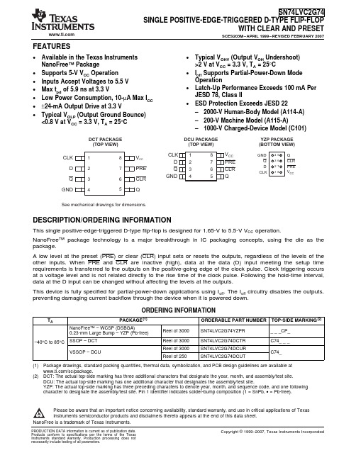
FEATURESSee mechanical drawings for dimensions.DCT PACKAGE (TOP VIEW)DCU PACKAGE (TOP VIEW)YZP PACKAGE (BOTTOM VIEW)CLK D Q GNDGND Q CLR Q PRE D V CCCLKDESCRIPTION/ORDERING INFORMATIONSN74LVC2G74SINGLE POSITIVE-EDGE-TRIGGERED D-TYPE FLIP-FLOPWITH CLEAR AND PRESETSCES203M–APRIL 1999–REVISED FEBRUARY 2007•Available in the Texas Instruments •Typical V OHV (Output V OH Undershoot)NanoFree™Package>2V at V CC =3.3V,T A =25°C•Supports 5-V V CC Operation •I off Supports Partial-Power-Down Mode Operation•Inputs Accept Voltages to 5.5V •Latch-Up Performance Exceeds 100mA Per •Max t pd of 5.9ns at 3.3VJESD 78,Class II•Low Power Consumption,10-µA Max I CC •ESD Protection Exceeds JESD 22•±24-mA Output Drive at 3.3V–2000-V Human-Body Model (A114-A)•Typical V OLP (Output Ground Bounce)–200-V Machine Model (A115-A)<0.8V at V CC =3.3V,T A =25°C–1000-V Charged-Device Model (C101)This single positive-edge-triggered D-type flip-flop is designed for 1.65-V to 5.5-V V CC operation.NanoFree™package technology is a major breakthrough in IC packaging concepts,using the die as the package.A low level at the preset (PRE)or clear (CLR)input sets or resets the outputs,regardless of the levels of the other inputs.When PRE and CLR are inactive (high),data at the data (D)input meeting the setup time requirements is transferred to the outputs on the positive-going edge of the clock pulse.Clock triggering occurs at a voltage level and is not related directly to the rise time of the clock pulse.Following the hold-time interval,data at the D input can be changed without affecting the levels at the outputs.This device is fully specified for partial-power-down applications using I off .The I off circuitry disables the outputs,preventing damaging current backflow through the device when it is powered down.ORDERING INFORMATIONT APACKAGE (1)ORDERABLE PART NUMBER TOP-SIDE MARKING (2)NanoFree™–WCSP (DSBGA)Reel of 3000SN74LVC2G74YZPR ___CP_0.23-mm Large Bump –YZP (Pb-free)SSOP –DCT Reel of 3000SN74LVC2G74DCTR C74___–40°C to 85°CReel of 3000SN74LVC2G74DCUR VSSOP –DCUC74_Reel of 250SN74LVC2G74DCUT(1)Package drawings,standard packing quantities,thermal data,symbolization,and PCB design guidelines are available at /sc/package.(2)DCT:The actual top-side marking has three additional characters that designate the year,month,and assembly/test site.DCU:The actual top-side marking has one additional character that designates the assembly/test site.YZP:The actual top-side marking has three preceding characters to denote year,month,and sequence code,and one following character to designate the assembly/test site.Pin 1identifier indicates solder-bump composition (1=SnPb,•=Pb-free).Please be aware that an important notice concerning availability,standard warranty,and use in critical applications of Texas Instruments semiconductor products and disclaimers thereto appears at the end of this data sheet.元器件交易网QQSN74LVC2G74SINGLE POSITIVE-EDGE-TRIGGERED D-TYPE FLIP-FLOP WITH CLEAR AND PRESETSCES203M–APRIL 1999–REVISED FEBRUARY 2007FUNCTION TABLEINPUTSOUTPUTSPRE CLR CLK D Q Q L H X X H L H L X X L H L L X X H (1)H (1)H H ↑H H L H H ↑L L H HHLXQ 0Q 0(1)This configuration is nonstable;that is,it does not persist when PRE or CLR returns to its inactive (high)level.LOGIC DIAGRAM (POSITIVE LOGIC)元器件交易网Absolute Maximum Ratings(1)SN74LVC2G74 SINGLE POSITIVE-EDGE-TRIGGERED D-TYPE FLIP-FLOPWITH CLEAR AND PRESETSCES203M–APRIL1999–REVISED FEBRUARY2007over operating free-air temperature range(unless otherwise noted)MIN MAX UNIT V CC Supply voltage range–0.5 6.5VV I Input voltage range(2)–0.5 6.5VV O Voltage range applied to any output in the high-impedance or power-off state(2)–0.5 6.5VV O Voltage range applied to any output in the high or low state(2)(3)–0.5V CC+0.5VI IK Input clamp current V I<0–50mAI OK Output clamp current V O<0–50mAI O Continuous output current±50mAContinuous current through V CC or GND±100mADCT package220θJA Package thermal impedance(4)DCU package227°C/WYZP package102 T stg Storage temperature range–65150°C(1)Stresses beyond those listed under"absolute maximum ratings"may cause permanent damage to the device.These are stress ratingsonly,and functional operation of the device at these or any other conditions beyond those indicated under"recommended operatingconditions"is not implied.Exposure to absolute-maximum-rated conditions for extended periods may affect device reliability.(2)The input negative-voltage and output voltage ratings may be exceeded if the input and output clamp-current ratings are observed.(3)The value of V CC is provided in the recommended operating conditions table.(4)The package thermal impedance is calculated in accordance with JESD51-7.元器件交易网Recommended Operating Conditions (1)SN74LVC2G74SINGLE POSITIVE-EDGE-TRIGGERED D-TYPE FLIP-FLOP WITH CLEAR AND PRESETSCES203M–APRIL 1999–REVISED FEBRUARY 2007MINMAX UNIT Operating1.65 5.5V CCSupply voltageVData retention only 1.5V CC =1.65V to 1.95V0.65×V CCV CC =2.3V to 2.7V 1.7V IHHigh-level input voltageVV CC =3V to 3.6V 2V CC =4.5V to 5.5V 0.7×V CCV CC =1.65V to 1.95V0.35×V CCV CC =2.3V to 2.7V 0.7V ILLow-level input voltageV V CC =3V to 3.6V 0.8V CC =4.5V to 5.5V0.3×V CCV I Input voltage 0 5.5V V OOutput voltage0V CC V V CC =1.65V –4V CC =2.3V–8I OHHigh-level output current–16mA V CC =3V –24V CC =4.5V –32V CC =1.65V 4V CC =2.3V8I OLLow-level output current16mA V CC =3V 24V CC =4.5V32V CC =1.8V ±0.15V,2.5V ±0.2V20∆t/∆v Input transition rise or fall rate V CC =3.3V ±0.3V 10ns/V V CC =5V ±0.5V5T A Operating free-air temperature–4085°C (1)All unused inputs of the device must be held at V CC or GND to ensure proper device operation.Refer to the TI application report,Implications of Slow or Floating CMOS Inputs ,literature number SCBA004.元器件交易网Electrical Characteristics Timing Requirements Switching CharacteristicsSN74LVC2G74 SINGLE POSITIVE-EDGE-TRIGGERED D-TYPE FLIP-FLOPWITH CLEAR AND PRESETSCES203M–APRIL1999–REVISED FEBRUARY2007over recommended operating free-air temperature range(unless otherwise noted)PARAMETER TEST CONDITIONS V CC MIN TYP(1)MAX UNITI OH=–100µA 1.65V to5.5V V CC–0.1I OH=–4mA 1.65V 1.2I OH=–8mA 2.3V 1.9V OH VI OH=–16mA 2.43VI OH=–24mA 2.3I OH=–32mA 4.5V 3.8I OL=100µA 1.65V to5.5V0.1I OL=4mA 1.65V0.45I OL=8mA 2.3V0.3V OL VI OL=16mA0.43VI OL=24mA0.55I OL=32mA 4.5V0.55Data orI I V I=5.5V or GND0to5.5V±5µAcontrol inputsI off V I or V O=5.5V0±10µAI CC V I=5.5V or GND,I O=0 1.65V to5.5V10µA∆I CC One input at V CC–0.6V,Other inputs at V CC or GND3V to5.5V500µAC i V I=V CC or GND 3.3V5pF(1)All typical values are at V CC=3.3V,T A=25°C.over recommended operating free-air temperature range(unless otherwise noted)(see Figure1)V CC=1.8V V CC=2.5V V CC=3.3V V CC=5V±0.15V±0.2V±0.3V±0.5V UNITMIN MAX MIN MAX MIN MAX MIN MAXf clock80175175200MHzCLK 6.2 2.7 2.72 t w Pulse duration nsPRE or CLR low 6.2 2.7 2.72Data 2.9 1.7 1.3 1.1 t su Setup time,before CLK↑nsPRE or CLR inactive 1.9 1.4 1.21 t h Hold time,data after CLK↑00.3 1.20.5nsover recommended operating free-air temperature range(unless otherwise noted)(see Figure1)V CC=1.8V V CC=2.5V V CC=3.3V V CC=5VFROM TO±0.15V±0.2V±0.3V±0.5V PARAMETER UNIT(INPUT)(OUTPUT)MIN MAX MIN MAX MIN MAX MIN MAXf max80175175200MHzQ 4.813.4 2.27.1 2.2 5.9 1.4 4.1CLKt pd Q614.437.7 2.6 6.2 1.6 4.4nsPRE or CLR Q or Q 4.412.9 2.37 1.7 5.9 1.6 4.1元器件交易网Operating CharacteristicsSN74LVC2G74SINGLE POSITIVE-EDGE-TRIGGERED D-TYPE FLIP-FLOP WITH CLEAR AND PRESETSCES203M–APRIL 1999–REVISED FEBRUARY 2007T A =25°CV CC =1.8VV CC =2.5VV CC =3.3VV CC =5V PARAMETERTEST CONDITIONSUNIT TYP TYP TYP TYP C pdPower dissipation capacitancef =10MHz35353740pF元器件交易网PARAMETER MEASUREMENT INFORMATIONFrom OutputUnder Test(see NoteLOAD CIRCUITOpenData InputTiming Input0 V0 V0 VInput0 VInputOutputWaveform 1S1 at V(see Note B)LOADOutputWaveform 2S1 at GND(see Note B)VOLVOH0 V»0 V OutputOutputTEST S1t/tPLH PHLOpenOutputControl1.8 V0.15 V±2.5 V0.2 V±3.3 V0.3 V±5 V0.5 V±1 k W500W500W500WVCCRL2 ×VCC2 ×VCC6 V2 ×VCCVLOADCL30 pF30 pF50 pF50 pF0.15 V0.15 V0.3 V0.3 VVD3 VVIVCC/2VCC/21.5 VVCC/2VM£2 ns£2 ns£2.5 ns£2.5 nsINPUTSt/tr fVCCVCCVCCVLOADt/tPLZ PZLGNDt/tPHZ PZHVOLTAGE WAVEFORMSENABLE AND DISABLE TIMESLOW-AND HIGH-LEVEL ENABLINGVOLTAGE WAVEFORMSPROPAGATION DELAY TIMESINVERTING AND NONINVERTING OUTPUTSNOTES: A.C includes probe and jig capacitance.B.Waveform 1 is for an output with internal conditions such that the output is low, except when disabled by the output control.Waveform 2 is for an output with internal conditions such that the output is high, except when disabled by the output control.C.All input pulses are supplied by generators having the following characteristics: PRR10 MHz, Z= 50.D.The outputs are measured one at a time, with one transition per measurement.E.t and t are the same as t.F.t and t are the same as t.G.t and t are the same as t.H.All parameters and waveforms are not applicable to all devices.LOPLZ PHZ disPZL PZH enPLH PHL pd£WVOLTAGE WAVEFORMSPULSE DURATIONVOLTAGE WAVEFORMSSETUP AND HOLD TIMESVIVIVIV/2LOADVOLVOHVIVIVOHVOLSN74LVC2G74SINGLE POSITIVE-EDGE-TRIGGERED D-TYPE FLIP-FLOPWITH CLEAR AND PRESETSCES203M–APRIL1999–REVISED FEBRUARY2007Figure1.Load Circuit and Voltage Waveforms元器件交易网PACKAGING INFORMATIONOrderable Device Status (1)Package Type Package Drawing Pins Package Qty Eco Plan (2)Lead/Ball Finish MSL Peak Temp (3)SN74LVC2G74DCTR ACTIVE SM8DCT 83000Green (RoHS &no Sb/Br)CU NIPDAU Level-1-260C-UNLIM SN74LVC2G74DCTRE4ACTIVE SM8DCT 83000Green (RoHS &no Sb/Br)CU NIPDAU Level-1-260C-UNLIM SN74LVC2G74DCUR ACTIVE US8DCU 83000Green (RoHS &no Sb/Br)CU NIPDAU Level-1-260C-UNLIM SN74LVC2G74DCURE4ACTIVE US8DCU 83000Green (RoHS &no Sb/Br)CU NIPDAU Level-1-260C-UNLIM SN74LVC2G74DCURG4ACTIVE US8DCU 83000Green (RoHS &no Sb/Br)CU NIPDAU Level-1-260C-UNLIM SN74LVC2G74DCUT ACTIVE US8DCU 8250Green (RoHS &no Sb/Br)CU NIPDAU Level-1-260C-UNLIM SN74LVC2G74DCUTE4ACTIVE US8DCU 8250Green (RoHS &no Sb/Br)CU NIPDAU Level-1-260C-UNLIM SN74LVC2G74DCUTG4ACTIVE US8DCU 8250Green (RoHS &no Sb/Br)CU NIPDAU Level-1-260C-UNLIM SN74LVC2G74YZPRACTIVEWCSPYZP83000Green (RoHS &no Sb/Br)SNAGCULevel-1-260C-UNLIM(1)The marketing status values are defined as follows:ACTIVE:Product device recommended for new designs.LIFEBUY:TI has announced that the device will be discontinued,and a lifetime-buy period is in effect.NRND:Not recommended for new designs.Device is in production to support existing customers,but TI does not recommend using this part in a new design.PREVIEW:Device has been announced but is not in production.Samples may or may not be available.OBSOLETE:TI has discontinued the production of the device.(2)Eco Plan -The planned eco-friendly classification:Pb-Free (RoHS),Pb-Free (RoHS Exempt),or Green (RoHS &no Sb/Br)-please check /productcontent for the latest availability information and additional product content details.TBD:The Pb-Free/Green conversion plan has not been defined.Pb-Free (RoHS):TI's terms "Lead-Free"or "Pb-Free"mean semiconductor products that are compatible with the current RoHS requirements for all 6substances,including the requirement that lead not exceed 0.1%by weight in homogeneous materials.Where designed to be soldered at high temperatures,TI Pb-Free products are suitable for use in specified lead-free processes.Pb-Free (RoHS Exempt):This component has a RoHS exemption for either 1)lead-based flip-chip solderbumps used between the die and package,or 2)lead-based die adhesive used between the die and leadframe.The component is otherwise considered Pb-Free (RoHS compatible)as defined above.Green (RoHS &no Sb/Br):TI defines "Green"to mean Pb-Free (RoHS compatible),and free of Bromine (Br)and Antimony (Sb)based flame retardants (Br or Sb do not exceed 0.1%by weight in homogeneous material)(3)MSL,Peak Temp.--The Moisture Sensitivity Level rating according to the JEDEC industry standard classifications,and peak solder temperature.Important Information and Disclaimer:The information provided on this page represents TI's knowledge and belief as of the date that it is provided.TI bases its knowledge and belief on information provided by third parties,and makes no representation or warranty as to the accuracy of such information.Efforts are underway to better integrate information from third parties.TI has taken and continues to take reasonable steps to provide representative and accurate information but may not have conducted destructive testing or chemical analysis on incoming materials and chemicals.TI and TI suppliers consider certain information to be proprietary,and thus CAS numbers and other limited information may not be available for release.In no event shall TI's liability arising out of such information exceed the total purchase price of the TI part(s)at issue in this document sold by TI to Customer on an annual basis.PACKAGE OPTION ADDENDUM6-Dec-2007TAPE AND REEL INFORMATION*All dimensions are nominalDevicePackage Type Package Drawing Pins SPQReel Diameter (mm)Reel Width W1(mm)A0(mm)B0(mm)K0(mm)P1(mm)W (mm)Pin1Quadrant SN74LVC2G74DCUR US8DCU83000180.09.22.253.35 1.054.08.0Q3*All dimensions are nominalDevice Package Type Package Drawing Pins SPQ Length(mm)Width(mm)Height(mm) SN74LVC2G74DCUR US8DCU83000202.0201.028.0IMPORTANT NOTICETexas Instruments Incorporated and its subsidiaries(TI)reserve the right to make corrections,modifications,enhancements,improvements, and other changes to its products and services at any time and to discontinue any product or service without notice.Customers should obtain the latest relevant information before placing orders and should verify that such information is current and complete.All products are sold subject to TI’s terms and conditions of sale supplied at the time of order acknowledgment.TI warrants performance of its hardware products to the specifications applicable at the time of sale in accordance with TI’s standard warranty.Testing and other quality control techniques are used to the extent TI deems necessary to support this warranty.Except where mandated by government requirements,testing of all parameters of each product is not necessarily performed.TI assumes no liability for applications assistance or customer product design.Customers are responsible for their products and applications using TI components.To minimize the risks associated with customer products and applications,customers should provide adequate design and operating safeguards.TI does not warrant or represent that any license,either express or implied,is granted under any TI patent right,copyright,mask work right, or other TI intellectual property right relating to any combination,machine,or process in which TI products or services are rmation published by TI regarding third-party products or services does not constitute a license from TI to use such products or services or a warranty or endorsement e of such information may require a license from a third party under the patents or other intellectual property of the third party,or a license from TI under the patents or other intellectual property of TI.Reproduction of TI information in TI data books or data sheets is permissible only if reproduction is without alteration and is accompanied by all associated warranties,conditions,limitations,and notices.Reproduction of this information with alteration is an unfair and deceptive business practice.TI is not responsible or liable for such altered rmation of third parties may be subject to additional restrictions.Resale of TI products or services with statements different from or beyond the parameters stated by TI for that product or service voids all express and any implied warranties for the associated TI product or service and is an unfair and deceptive business practice.TI is not responsible or liable for any such statements.TI products are not authorized for use in safety-critical applications(such as life support)where a failure of the TI product would reasonably be expected to cause severe personal injury or death,unless officers of the parties have executed an agreement specifically governing such use.Buyers represent that they have all necessary expertise in the safety and regulatory ramifications of their applications,and acknowledge and agree that they are solely responsible for all legal,regulatory and safety-related requirements concerning their products and any use of TI products in such safety-critical applications,notwithstanding any applications-related information or support that may be provided by TI.Further,Buyers must fully indemnify TI and its representatives against any damages arising out of the use of TI products in such safety-critical applications.TI products are neither designed nor intended for use in military/aerospace applications or environments unless the TI products are specifically designated by TI as military-grade or"enhanced plastic."Only products designated by TI as military-grade meet military specifications.Buyers acknowledge and agree that any such use of TI products which TI has not designated as military-grade is solely at the Buyer's risk,and that they are solely responsible for compliance with all legal and regulatory requirements in connection with such use. TI products are neither designed nor intended for use in automotive applications or environments unless the specific TI products are designated by TI as compliant with ISO/TS16949requirements.Buyers acknowledge and agree that,if they use any non-designated products in automotive applications,TI will not be responsible for any failure to meet such requirements.Following are URLs where you can obtain information on other Texas Instruments products and application solutions:Products ApplicationsAmplifiersAudioData Converters AutomotiveDSP BroadbandClocks and Timers Digital ControlInterface MedicalLogic MilitaryPower Mgmt Optical NetworkingMicrocontrollers SecurityRFID TelephonyRF/IF and ZigBee®Solutions Video&ImagingWirelessMailing Address:Texas Instruments,Post Office Box655303,Dallas,Texas75265Copyright©2008,Texas Instruments Incorporated元器件交易网。
常用74系列标准数字电路的中文名称资料

常用74系列标准数字电路的中文名称资料2010-11-30 00:047400 TTL 2输入端四与非门7401 TTL 集电极开路2输入端四与非门7402 TTL 2输入端四或非门7403 TTL 集电极开路2输入端四与非门7404 TTL 六反相器7405 TTL 集电极开路六反相器7406 TTL 集电极开路六反相高压驱动器7407 TTL 集电极开路六正相高压驱动器7408 TTL 2输入端四与门7409 TTL 集电极开路2输入端四与门7410 TTL 3输入端3与非门74107 TTL 带清除主从双J-K触发器74109 TTL 带预置清除正触发双J-K触发器7411 TTL 3输入端3与门74112 TTL 带预置清除负触发双J-K触发器7412 TTL 开路输出3输入端三与非门74121 TTL 单稳态多谐振荡器74122 TTL 可再触发单稳态多谐振荡器74123 TTL 双可再触发单稳态多谐振荡器74125 TTL 三态输出高有效四总线缓冲门74126 TTL 三态输出低有效四总线缓冲门7413 TTL 4输入端双与非施密特触发器74132 TTL 2输入端四与非施密特触发器74133 TTL 13输入端与非门74136 TTL 四异或门74138 TTL 3-8线译码器/复工器74139 TTL 双2-4线译码器/复工器7414 TTL 六反相施密特触发器74145 TTL BCD—十进制译码/驱动器7415 TTL 开路输出3输入端三与门74150 TTL 16选1数据选择/多路开关74151 TTL 8选1数据选择器74153 TTL 双4选1数据选择器74154 TTL 4线—16线译码器74155 TTL 图腾柱输出译码器/分配器74156 TTL 开路输出译码器/分配器74157 TTL 同相输出四2选1数据选择器74158 TTL 反相输出四2选1数据选择器7416 TTL 开路输出六反相缓冲/驱动器74160 TTL 可预置BCD异步清除计数器74161 TTL 可予制四位二进制异步清除计数器74162 TTL 可预置BCD同步清除计数器74163 TTL 可予制四位二进制同步清除计数器74164 TTL 八位串行入/并行输出移位寄存器74165 TTL 八位并行入/串行输出移位寄存器74166 TTL 八位并入/串出移位寄存器74169 TTL 二进制四位加/减同步计数器7417 TTL 开路输出六同相缓冲/驱动器74170 TTL 开路输出4×4寄存器堆74173 TTL 三态输出四位D型寄存器74174 TTL 带公共时钟和复位六D触发器74175 TTL 带公共时钟和复位四D触发器74180 TTL 9位奇数/偶数发生器/校验器74181 TTL 算术逻辑单元/函数发生器74185 TTL 二进制—BCD代码转换器74190 TTL BCD同步加/减计数器74191 TTL 二进制同步可逆计数器74192 TTL 可预置BCD双时钟可逆计数器74193 TTL 可预置四位二进制双时钟可逆计数器74194 TTL 四位双向通用移位寄存器74195 TTL 四位并行通道移位寄存器74196 TTL 十进制/二-十进制可预置计数锁存器74197 TTL 二进制可预置锁存器/计数器7420 TTL 4输入端双与非门7421 TTL 4输入端双与门7422 TTL 开路输出4输入端双与非门74221 TTL 双/单稳态多谐振荡器74240 TTL 八反相三态缓冲器/线驱动器74241 TTL 八同相三态缓冲器/线驱动器74243 TTL 四同相三态总线收发器74244 TTL 八同相三态缓冲器/线驱动器74245 TTL 八同相三态总线收发器74247 TTL BCD—7段15V输出译码/驱动器74248 TTL BCD—7段译码/升压输出驱动器74249 TTL BCD—7段译码/开路输出驱动器74251 TTL 三态输出8选1数据选择器/复工器74253 TTL 三态输出双4选1数据选择器/复工器74256 TTL 双四位可寻址锁存器74257 TTL 三态原码四2选1数据选择器/复工器74258 TTL 三态反码四2选1数据选择器/复工器74259 TTL 八位可寻址锁存器/3-8线译码器7426 TTL 2输入端高压接口四与非门74260 TTL 5输入端双或非门74266 TTL 2输入端四异或非门7427 TTL 3输入端三或非门74273 TTL 带公共时钟复位八D触发器74279 TTL 四图腾柱输出S-R锁存器7428 TTL 2输入端四或非门缓冲器74283 TTL 4位二进制全加器74290 TTL 二/五分频十进制计数器74293 TTL 二/八分频四位二进制计数器74295 TTL 四位双向通用移位寄存器74298 TTL 四2输入多路带存贮开关74299 TTL 三态输出八位通用移位寄存器7430 TTL 8输入端与非门7432 TTL 2输入端四或门74322 TTL 带符号扩展端八位移位寄存器74323 TTL 三态输出八位双向移位/存贮寄存器7433 TTL 开路输出2输入端四或非缓冲器74347 TTL BCD—7段译码器/驱动器74352 TTL 双4选1数据选择器/复工器74353 TTL 三态输出双4选1数据选择器/复工器74365 TTL 门使能输入三态输出六同相线驱动器74365 TTL 门使能输入三态输出六同相线驱动器74366 TTL 门使能输入三态输出六反相线驱动器74367 TTL 4/2线使能输入三态六同相线驱动器74368 TTL 4/2线使能输入三态六反相线驱动器7437 TTL 开路输出2输入端四与非缓冲器74373 TTL 三态同相八D锁存器74374 TTL 三态反相八D锁存器74375 TTL 4位双稳态锁存器74377 TTL 单边输出公共使能八D锁存器74378 TTL 单边输出公共使能六D锁存器74379 TTL 双边输出公共使能四D锁存器7438 TTL 开路输出2输入端四与非缓冲器74380 TTL 多功能八进制寄存器7439 TTL 开路输出2输入端四与非缓冲器74390 TTL 双十进制计数器74393 TTL 双四位二进制计数器7440 TTL 4输入端双与非缓冲器7442 TTL BCD—十进制代码转换器74352 TTL 双4选1数据选择器/复工器74353 TTL 三态输出双4选1数据选择器/复工器74365 TTL 门使能输入三态输出六同相线驱动器74366 TTL 门使能输入三态输出六反相线驱动器74367 TTL 4/2线使能输入三态六同相线驱动器74368 TTL 4/2线使能输入三态六反相线驱动器7437 TTL 开路输出2输入端四与非缓冲器74373 TTL 三态同相八D锁存器74374 TTL 三态反相八D锁存器74375 TTL 4位双稳态锁存器74377 TTL 单边输出公共使能八D锁存器74378 TTL 单边输出公共使能六D锁存器74379 TTL 双边输出公共使能四D锁存器7438 TTL 开路输出2输入端四与非缓冲器74380 TTL 多功能八进制寄存器7439 TTL 开路输出2输入端四与非缓冲器74390 TTL 双十进制计数器74393 TTL 双四位二进制计数器7440 TTL 4输入端双与非缓冲器7442 TTL BCD—十进制代码转换器74447 TTL BCD—7段译码器/驱动器7445 TTL BCD—十进制代码转换/驱动器74450 TTL 16:1多路转接复用器多工器74451 TTL 双8:1多路转接复用器多工器74453 TTL 四4:1多路转接复用器多工器7446 TTL BCD—7段低有效译码/驱动器74460 TTL 十位比较器74461 TTL 八进制计数器74465 TTL 三态同相2与使能端八总线缓冲器74466 TTL 三态反相2与使能八总线缓冲器74467 TTL 三态同相2使能端八总线缓冲器74468 TTL 三态反相2使能端八总线缓冲器74469 TTL 八位双向计数器7447 TTL BCD—7段高有效译码/驱动器7448 TTL BCD—7段译码器/内部上拉输出驱动74490 TTL 双十进制计数器74491 TTL 十位计数器74498 TTL 八进制移位寄存器7450 TTL 2-3/2-2输入端双与或非门74502 TTL 八位逐次逼近寄存器74503 TTL 八位逐次逼近寄存器7451 TTL 2-3/2-2输入端双与或非门74533 TTL 三态反相八D锁存器74534 TTL 三态反相八D锁存器7454 TTL 四路输入与或非门74540 TTL 八位三态反相输出总线缓冲器7455 TTL 4输入端二路输入与或非门74563 TTL 八位三态反相输出触发器74564 TTL 八位三态反相输出D触发器74573 TTL 八位三态输出触发器74574 TTL 八位三态输出D触发器74645 TTL 三态输出八同相总线传送接收器74670 TTL 三态输出4×4寄存器堆7473 TTL 带清除负触发双J-K触发器7474 TTL 带置位复位正触发双D触发器7476 TTL 带预置清除双J-K触发器7483 TTL 四位二进制快速进位全加器7485 TTL 四位数字比较器7486 TTL 2输入端四异或门7490 TTL 可二/五分频十进制计数器7493 TTL 可二/八分频二进制计数器7495 TTL 四位并行输入\输出移位寄存器7497 TTL 6位同步二进制乘法器SN74LSOO四2输入与非门SN74LSO2四2输入或非门SN74LS04六反相器SN74LS06六反相缓冲器/驱动器SN74LS08四2输入与非门SN74LS10三3输入与非门SN74LS12三3输入与非门SN74LS14六反相器.斯密特触发SN74LS16六反相缓冲器/驱动器SN74LS20双4输入与门SN74LS22双4输入与门SN74LS26四2输入与非门SN74LS28四输入端或非缓冲器SN74LS32四2输入或门SN74LS37四输入端与非缓冲器SN74LS40四输入端与非缓冲器SN74LS47BCD-七段译码驱动器SN74LS49BCD-七段译码驱动器SN74LS54四输入与或非门SN74LS63六电流读出接口门SN74LS74双D触发器SN74LS76双J-K触发器SN74LS83双J-K触发器SN74LS86四2输入异或门SN74LS904位十进制波动计数器SN74LS9212分频计数器SN74LS965位移位寄存器SN74LS109正沿触发双J-K触发器SN74LS113双J-K负沿触发器SN74LS121单稳态多谐振荡器SN74LS123双稳态多谐振荡器SN74LS125三态缓冲器SN74LS1313-8线译码器SN74LS137地址锁存3-8线译码器SN74LS139双2-4线译码-转换器SN74LS14710-4线优先编码器SN74LS153双4选1数据选择器SN74LS155双2-4线多路分配器SN74LS157四2选1数据选择器SN74LS160同步BDC十进制计数器SN74LS162同步BDC十进制计数器SN74LS1648位串入并出移位寄存SN74LS1668位移位寄存器SN74LS1694位可逆同步计数器SN74LS17216位多通道寄存器堆SN74LS1746D型触发器SN74LS176可预置十进制计数器SN74LS182超前进位发生器SN74LS18964位随机存储器SN74LS191二进制同步可逆计数器SN74LS193二进制可逆计数器SN74LS195并行存取移位寄存器SN74LS197可预置二进制计数器SN74LS2383-8线译码/多路转换器SN74LS241八缓冲/驱动/接收器SN74LS243四总线收发器SN74LS245八总线收发器SN74LS248BCD-七段译码驱动器SN74LS251三态8-1数据选择器SN74LS256双四位选址锁存器SN74LS258四2选1数据选择器SN74LS260双5输入或非门SN74LS266四2输入异或非门SN74LS275七位树型乘法器SN74LS279四R-S触发器SN74LS2834位二进制全加器SN74LS2934位二进制计数器SN74LS365六缓冲器带公用启动器SN74LS367六总线三态输出缓冲器SN74LS3738D锁存器SN74LS3754位双稳锁存器SN74LS386四2输入异或门SN74LS393双4位二进制计数器SN74LS5748位D型触发器SN74LS6848位数字比较器SN74LSO1四2输入与非门SN74LS05六反相器SN74LS07六缓冲器/驱动器SN74LS09四2输入与非门SN74LS11三3输入与非门SN74LS13三3输入与非门SN74LS15三3输入与非门SN74LS17六反相缓冲器/驱动器SN74LS21双4输入与门SN74LS25双4输入与门SN74LS27三3输入与非门SN74LS30八输入端与非门SN74LS33四2输入或门SN74LS38双2输入与非缓冲器SN74LS42BCD-十进制译码器SN74LS48BCD-七段译码驱动器SN74LS51三3输入双与或非门SN74LS55四4输入与或非门SN74LS73双J-K触发器SN74LS754位双稳锁存器SN74LS78双J-K触发器SN74LS854位幅度比较器SN74LS884位全加器SN74LS918位移位寄存器SN74LS93二进制计数器SN74LS954位并入并出寄存器SN74LS107双J-K触发器SN74LS112双J-K负沿触发器SN74LS114双J-K负沿触发器SN74LS122单稳态多谐振荡器SN74LS124双压控振荡器SN74LS126四3态总线缓冲器SN74LS132二输入与非触发器SN74LS136四异或门SN74LS1383-8线译码/转换器SN74LS145BCD十进制译码/驱动器SN74LS1488-3线优先编码器SN74LS1518选1数据选择器SN74LS1544-16线多路分配器SN74LS156双2-4线多路分配器SN74LS158四2选1数据选择器SN74LS1614位二进制计数器SN74LS1634位二进制计数器SN74LS1658位移位寄存器SN74LS1684位可逆同步计数器SN74LS1704x4位寄存器堆SN74LS1734D型寄存器SN74LS1754D烯触发器SN74LS181运算器/函数发生器SN74LS183双进位保存全价器SN74LS190同步BCD十进制计数器SN74LS192BCD-同步可逆计数器SN74LS194双向通用移位寄存器SN74LS196可预置十进制计数器SN74LS221双单稳态多谐振荡器SN74LS240八缓冲/驱动/接收器SN74LS242四总线收发器SN74LS244八缓冲/驱动/接收器SN74LS247BCD-七段译码驱动器SN74LS249BCD-七段译码驱动SN74LS253双三态4-1数据选择器SN74LS257四3态2-1数据选择器SN74LS2598位可寻址锁存器SN74LS2612x4位二进制乘发器SN74LS273八进制D型触发器SN74LS276四J-K触发器SN74LS2809位奇偶数发生校检器SN74LS290十进制计数器SN74LS2954位双向通用移位寄存器SN74LS366六缓冲器带公用启动器SN74LS368六总线三态输出反相器SN74LS3748D触发器SN74LS3778位单输出D型触发器SN74LS390双十进制计数器SN74LS5738位三态输出D型锁存器SN74LS6708位数字比较器SN74HC00 四2输入与非门SN74HC02 四2输入或非门SN74HC03 四2输入或非门SN74HC04 六反相器SN74HC05 六反相器SN74HC08 四2输入与门SN74HC10 三3输入与非门SN74HC11 三3输入与门SN74HC14 六反相器/斯密特触发SN74HC20 双四输入与门SN74HC21 双四输入与非门SN74HC27 三3输入与非门SN74HC30 八输入端与非门SN74HC32 四2输入或门SN74HC42 BCD十进制译码器SN74HC73 双J-K触的器SN74HC74 双D型触发器SN74HC76 双J-K触的器SN74HC86 四2输入异或门SN74HC107 双J-K触发器SN74HC113 双J-K负沿触发器SN74HC123 双稳态多谐振荡器SN74HC125 三态缓冲器SN74HC126 四三态总线缓冲器SN74HC132 二输入与非缓冲器SN74HC137 二输入与非缓冲器SN74HC138 3-8线译码/解调器SN74HC139 双2-4线译码/解调器SN74HC148 8选1数据选择器SN74HC151 双4选1数据选择器SN74HC154 4-16线多路分配器SN74HC157 四2选1数据选择器SN74HC161 4位二进制计数器SN74HC163 4位二进制计数器SN74HC164 8位串入并出移位寄存器SN74HC165 8位移位寄存器SN74HC173 4D型触发器SN74HC174 6D触发器SN74HC175 4D型触发器SN74HC191 二进制同步可逆计数器SN74HC221 双单稳态多谐振荡器SN74HC238 3-8线译码器SN74HC240 八缓冲器SN74HC244 八总线3态输出缓冲器SN74HC245 八总线收发器SN74HC251 三态8-1数据选择器SN74HC259 8位可寻址锁存器SN74HC266 四2输入异或非门SN74HC273 8D型触发器SN74HC367 六缓冲器/总线驱动器SN74HC368 六缓冲器/总线驱动器SN74HC373 8D锁存器SN74HC374 8D触发器SN74HC393 双4位二进制计数器SN74HC541 8位三态输出缓冲器SN74HC573 8位三态输出D型锁存器SN74HC574 8D型触发器SN74HC595 8位移位寄存器/锁存器SN74HC4028 7级二进制串行加数器SN74HC4046 锁相环SN74HC4050 六同相缓冲器SN74HC4051 8选1模拟开关SN74HC4053 三2选1模拟开关SN74HC4060 14位计数/分频/振荡器SN74HC4066 四双相模拟开关SN74HC4078 3输入端三或门SN74HC4511 7段锁存/译码驱动器SN74HC4520 双二进制加法计数器74F00 高速四2输入与非门74F02 高速四2输入或非门74F04 高速六反相器74F08 高速四2输入与门74F10 高速三3输入与门74F14 高速六反相斯密特触发74F32 高速四2输入或门74F38 高速四2输入或门74F74 高速双D型触发器74F86 高速四2输入异或门74F139 高速双2-4线译码/驱动器74F151 高速双2-4线译码/驱动器74F153 高速双4选1数据选择器74F157 高速双4选1数据选择器74F161 高速6D型触发器74F174 高速6D型触发器74F175 高速4D型触发器74F244 高速八总线3态缓冲器74F245 高速八总线收发器74F373 高速8D锁存器SN74HCT04 六反相器SN7404 六反相器 SN74HC00 四2输入与非门SN7406 六反相缓冲器/驱动器 SN74HC02 四2输入或非门SN7407 六缓冲器/驱动器 SN74HC03 四2输入或非门SN7414 六缓冲器/驱动器 SN74HC04 六反相器SN7416 六反相缓冲器/驱动器 SN74HC05 六反相器SN7440 六反相缓冲器/驱动器 SN74HC08 四2输入与门SN7497 六反相缓冲器/驱动器 SN74HC10 三3输入与非门74F00 高速四2输入与非门 SN74HC14 六反相器/斯密特触发74F02 高速四2输入或非门 SN74HC20 双四输入与门74F04 高速六反相器 SN74HC21 双四输入与非门74F08 高速四2输入与门 SN74HC27 三3输入与非门74F10 高速三3输入与门 SN74HC30 八输入端与非门74F14 高速六反相斯密特触发 SN74HC32 四2输入或门74F32 高速四2输入或门 SN74HC42 BCD十进制译码器74F38 高速四2输入或门 SN74HC73 双J-K触的器74F74 高速双D型触发器 SN74HC74 双D型触发器74F86 高速四2输入异或门 SN74HC76 双J-K触的器74F139 高速双2-4线译码/驱动器 SN74HC86 四2输入异或门74F151 高速双2-4线译码/驱动器 SN74HC107 双J-K触发器74F153 高速双4选1数据选择器 SN74HC113 双J-K负沿触发器74F157 高速双4选1数据选择器 SN74HC123 双稳态多谐振荡器74F161 高速6D型触发器 SN74HC125 三态缓冲器74F174 高速6D型触发器 SN74HC126 四三态总线缓冲器74F175 高速4D型触发器 SN74HC132 二输入与非缓冲器74F244 高速八总线3态缓冲器 SN74HC137 二输入与非缓冲器74F245 高速八总线收发器 SN74HC138 3-8线译码/解调器74F373 高速8D锁存器 SN74HC139 双2-4线译码/SN74HCT04 六反相器 SN74HC151 双4选1数据选择器CD4001 4二输入或非门 SN74HC157 四2选1数据选择器CD4002 双4输入或非门 SN74HC161 4位二进制计数器CD4006 18位静态移位寄存器 SN74HC163 4位二进制计数器CD4007 双互补对加反相器 SN74HC164 8位串入并出移位寄存器CD4009 六缓冲器/转换-倒相 SN74HC165 8位移位寄存器CD4010 六缓冲器/转换-正相 SN74HC173 4D型触发器CD4011 四2输入与非门 SN74HC174 6D触发器CD4012 双4输入与非门 SN74HC175 4D型触发器CD4013 置/复位双D型触发器 SN74HC191 二进制同步可逆计数器CD4014 8位静态同步移位寄存 SN74HC221 双单稳态多谐振荡器CD4015 双4位静态移位寄存器 SN74HC238 3-8线译码器CD4016 四双向模拟数字开关 SN74HC240 八缓冲器CD4017 10译码输出十进制计数器 SN74HC244 八总线3态输出缓冲器CD4018 可预置1/N计数器 SN74HC245 八总线收发器CD4019 四与或选择门 SN74HC251 三态8-1数据选择器CD4020 14位二进制计数器 SN74HC259 8位可寻址锁存器CD4021 8位静态移位寄存器 SN74HC266 四2输入异或非门CD4022 8译码输出8进制计数器 SN74HC273 8D型触发器CD4023 三3输入与非门 SN74HC367 六缓冲器/总线CD4024 7位二进制脉冲计数器 SN74HC368 六缓冲器/总线驱动器CD4025 三3输入与非门 SN74HC373 8D锁存器CD4026 十进制/7段译码/驱动 SN74HC374 8D触发器CD4027 置位/复位主从触发器 SN74HC393 双4位二进制计数器CD4028 BCD十进制译码器 SN74HC541 8位三态输出缓冲器CD4029 4位可预置可逆计数器 SN74HC573 8位三态输出D型锁存器CD4030 四异或门 SN74HC574 8D型触发器CD4031 64位静态移位寄存器 SN74HC595 8位移位寄存器/锁存器CD4032 三串行加法器 SN74HC4028 7级二进制串行加数器CD4033 十进制计数器/7段显示 SN74HC4046 锁相环CD4034 8位静态移位寄存器 SN74HC4050 六同相缓冲器CD4035 4位并入/并出移位寄存器 SN74HC4051 8选1模拟开关CD4038 3位串行加法器 SN74HC4053 三2选1模拟开关CD4040 12位二进制计数器 SN74HC4060 14位计数/分频/振荡器CD4041 四原码/补码缓冲器 SN74HC4066 四双相模拟开关CD4042 四时钟D型锁存器 SN74HC4078 3输入端三或门CD4043 四或非R/S锁存器 SN74HC4511 7段锁存/译码驱动器CD4044 四与非R/S锁存器 SN74HC4520 双二进制加法计数器。
74LVC2G240中文资料
74LVC2G240
MAX. 5.5 5.5 VCC 5.5 5.5 +125 20 10 V V V V V
UNIT
°C ns/V ns/V
LIMITING VALUES In accordance with the Absolute Maximum Rating System (IEC 60134); voltages are referenced to GND (ground = 0 V). SYMBOL VCC IIK VI IOK VO PARAMETER supply voltage input diode current input voltage output diode current output voltage VI < 0 note 1 VO > VCC or VO < 0 enable mode; notes 1 and 2 disable mode; notes 1 and 2 IO ICC, IGND Tstg PD Notes 1. The input and output voltage ratings may be exceeded if the input and output current ratings are observed. 2. When VCC = 0 V (Power-down mode), the output voltage can be 5.5 V in normal operation. 3. Above 110 °C the value of PD derates linearly with 8 mW/K. output source or sink current VCC or GND current storage temperature power dissipation Tamb = −40 to +125 °C; note 3 VO = 0 to VCC CONDITIONS − −0.5 − −0.5 −0.5 − − −65 − MIN. −0.5 MAX. +6.5 −50 +6.5 ±50 +6.5 +6.5 ±50 ±100 +150 300 V mA V mA V V mA mA °C mW UNIT
74系列中文资料(非常全)
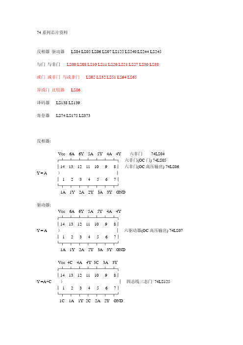
74系列芯片资料反相器驱动器LS04 LS05 LS06 LS07 LS125 LS240 LS244 LS245与门与非门LS00 LS08 LS10 LS11 LS20 LS21 LS27 LS30 LS38或门或非门与或非门LS02 LS32 LS51 LS64 LS65异或门比较器LS86译码器LS138 LS139寄存器LS74 LS175 LS373反相器:Vcc 6A 6Y 5A 5Y 4A 4Y 六非门74LS04┌┴─┴─┴─┴─┴─┴─┴┐六非门(OC门) 74LS05 _ │14 13 12 11 10 9 8│六非门(OC高压输出) 74LS06 Y = A )││1 2 3 4 5 6 7│└┬─┬─┬─┬─┬─┬─┬┘1A 1Y 2A 2Y 3A 3Y GND驱动器:Vcc 6A 6Y 5A 5Y 4A 4Y┌┴─┴─┴─┴─┴─┴─┴┐│14 13 12 11 10 9 8│Y = A )│六驱动器(OC高压输出) 74LS07 │1 2 3 4 5 6 7│└┬─┬─┬─┬─┬─┬─┬┘1A 1Y 2A 2Y 3A 3Y GNDVcc -4C 4A 4Y -3C 3A 3Y┌┴─┴─┴─┴─┴─┴─┴┐_ │14 13 12 11 10 9 8│Y =A+C )│四总线三态门74LS125 │1 2 3 4 5 6 7│└┬─┬─┬─┬─┬─┬─┬┘-1C 1A 1Y -2C 2A 2Y GNDVcc -G B1 B2 B3 B4 B8 B6 B7 B8┌┴─┴─┴─┴─┴─┴─┴─┴─┴─┴┐8位总线驱动器74LS245 │20 19 18 17 16 15 14 13 12 11│)│DIR=1 A=>B│1 2 3 4 5 6 7 8 9 10│DIR=0 B=>A└┬─┬─┬─┬─┬─┬─┬─┬─┬─┬┘DIR A1 A2 A3 A4 A5 A6 A7 A8 GND正逻辑与门,与非门:Vcc 4B 4A 4Y 3B 3A 3Y┌┴─┴─┴─┴─┴─┴─┴┐│14 13 12 11 10 9 8│Y = AB )│2输入四正与门74LS08 │1 2 3 4 5 6 7│└┬─┬─┬─┬─┬─┬─┬┘1A 1B 1Y 2A 2B 2Y GNDVcc 4B 4A 4Y 3B 3A 3Y┌┴─┴─┴─┴─┴─┴─┴┐__ │14 13 12 11 10 9 8│Y = AB )│2输入四正与非门74LS00 │1 2 3 4 5 6 7│└┬─┬─┬─┬─┬─┬─┬┘1A 1B 1Y 2A 2B 2Y GNDVcc 1C 1Y 3C 3B 3A 3Y┌┴─┴─┴─┴─┴─┴─┴┐___ │14 13 12 11 10 9 8│Y = ABC )│3输入三正与非门74LS10 │1 2 3 4 5 6 7│└┬─┬─┬─┬─┬─┬─┬┘1A 1B 2A 2B 2C 2Y GNDVcc H G Y┌┴─┴─┴─┴─┴─┴─┴┐│14 13 12 11 10 9 8│)│8输入与非门74LS30│1 2 3 4 5 6 7│________└┬─┬─┬─┬─┬─┬─┬┘Y = ABCDEFGHA B C D E F GND正逻辑或门,或非门:Vcc 4B 4A 4Y 3B 3A 3Y┌┴─┴─┴─┴─┴─┴─┴┐2输入四或门74LS32│14 13 12 11 10 9 8│)│Y = A+B│1 2 3 4 5 6 7│└┬─┬─┬─┬─┬─┬─┬┘1A 1B 1Y 2A 2B 2Y GNDVcc 4Y 4B 4A 3Y 3B 3A┌┴─┴─┴─┴─┴─┴─┴┐2输入四或非门74LS02│14 13 12 11 10 9 8│___)│Y = A+B│1 2 3 4 5 6 7│└┬─┬─┬─┬─┬─┬─┬┘1Y 1A 1B 2Y 2A 2B GNDVcc 2Y 2B 2A 2D 2E 1F┌┴─┴─┴─┴─┴─┴─┴┐双与或非门74S51│14 13 12 11 10 9 8│_____)│2Y = AB+DE│1 2 3 4 5 6 7│_______└┬─┬─┬─┬─┬─┬─┬┘1Y = ABC+DEF1Y 1A 1B 1C 1D 1E GNDVcc D C B K J Y┌┴─┴─┴─┴─┴─┴─┴┐4-2-3-2与或非门74S64 74S65(OC门) │14 13 12 11 10 9 8│______________)│Y = ABCD+EF+GHI+JK│1 2 3 4 5 6 7│└┬─┬─┬─┬─┬─┬─┬┘A E F G H I GND页首非门,驱动器与门,与非门或门,或非门异或门,比较器译码器寄存器2输入四异或门74LS86Vcc 4B 4A 4Y 3Y 3B 3A┌┴─┴─┴─┴─┴─┴─┴┐│14 13 12 11 10 9 8│)│_ _│1 2 3 4 5 6 7│Y=AB+AB└┬─┬─┬─┬─┬─┬─┬┘1A 1B 1Y 2Y 2A 2B GND8*2输入比较器74LS688_Vcc Y B8 A8 B7 A7 B6 A6 B5 A5┌┴─┴─┴─┴─┴─┴─┴─┴─┴─┴┐8*2输入比较器74LS688│20 19 18 17 16 15 14 13 12 11│)││1 2 3 4 5 6 7 8 9 10│└┬─┬─┬─┬─┬─┬─┬─┬─┬─┬┘CE A1 B1 A2 B2 A3 B3 A4 B4 GND_Y=A1⊙B1+A2⊙B2+A3⊙B3+A4⊙B4+A5⊙B5+A6⊙B6+A7⊙B7+A8⊙B83-8译码器74LS138Vcc -Y0 -Y1 -Y2 -Y3 -Y4 -Y5 -Y6 __ _ _ _ __ _ _ __ _ _ __ _┌┴─┴─┴─┴─┴─┴─┴─┴┐Y0=A B C Y1=A B C Y2=A B C Y3=A B C│16 15 14 13 12 11 10 9 │)│__ _ _ __ _ __ _ __│1 2 3 4 5 6 7 8│Y4=A B C Y5=A B C Y6=A B C Y7=A B C└┬─┬─┬─┬─┬─┬─┬─┬┘A B C -CS0 -CS1 CS2 -Y7 GND双2-4译码器74LS139Vcc -2G 2A 2B -Y0 -Y1 -Y2 -Y3 __ __ __ __ __ __ __ __┌┴─┴─┴─┴─┴─┴─┴─┴┐Y0=2A 2B Y1=2A 2B Y2=2A 2B Y3=2A 2B│16 15 14 13 12 11 10 9 │)│__ __ __ __ __ __ __ __│ 1 2 3 4 5 6 7 8│Y0=1A 1B Y1=1A 1B Y2=1A 1B Y3=1A 1B└┬─┬─┬─┬─┬─┬─┬─┬┘-1G 1A 1B -Y0 -Y1 -Y2 -Y3 GND8*2输入比较器74LS688_Vcc Y B8 A8 B7 A7 B6 A6 B5 A5┌┴─┴─┴─┴─┴─┴─┴─┴─┴─┴┐8*2输入比较器74LS688 │20 19 18 17 16 15 14 13 12 11│)││1 2 3 4 5 6 7 8 9 10│└┬─┬─┬─┬─┬─┬─┬─┬─┬─┬┘CE A1 B1 A2 B2 A3 B3 A4 B4 GND_Y=A1⊙B1+A2⊙B2+A3⊙B3+A4⊙B4+A5⊙B5+A6⊙B6+A7⊙B7+A8⊙B8寄存器:Vcc 2CR 2D 2Ck 2St 2Q -2Q┌┴─┴─┴─┴─┴─┴─┴┐双D触发器74LS74│14 13 12 11 10 9 8 │)││1 2 3 4 5 6 7│└┬─┬─┬─┬─┬─┬─┬┘1Cr 1D 1Ck 1St 1Q -1Q GNDVcc 8Q 8D 7D 7Q 6Q 6D 5D 5Q ALE┌┴─┴─┴─┴─┴─┴─┴─┴─┴─┴┐8位锁存器74LS373│20 19 18 17 16 15 14 13 12 11│)││1 2 3 4 5 6 7 8 9 10│└┬─┬─┬─┬─┬─┬─┬─┬─┬─┬┘-OE 1Q 1D 2D 2Q 3Q 3D 4D 4Q GND--------------------------------------------------------------------------------常见数字逻辑器件中文注解74系列:74LS00 TTL 2输入端四与非门74LS01 TTL 集电极开路2输入端四与非门74LS02 TTL 2输入端四或非门74LS03 TTL 集电极开路2输入端四与非门74LS04 TTL 六反相器74LS05 TTL 集电极开路六反相器74LS06 TTL 集电极开路六反相高压驱动器74LS07 TTL 集电极开路六正相高压驱动器74LS08 TTL 2输入端四与门74LS09 TTL 集电极开路2输入端四与门74LS10 TTL 3输入端3与非门74LS107 TTL 带清除主从双J-K触发器74LS109 TTL 带预置清除正触发双J-K触发器74LS11 TTL 3输入端3与门74LS112 TTL 带预置清除负触发双J-K触发器74LS12 TTL 开路输出3输入端三与非门74LS121 TTL 单稳态多谐振荡器74LS122 TTL 可再触发单稳态多谐振荡器74LS123 TTL 双可再触发单稳态多谐振荡器74LS125 TTL 三态输出高有效四总线缓冲门74LS126 TTL 三态输出低有效四总线缓冲门74LS13 TTL 4输入端双与非施密特触发器74LS132 TTL 2输入端四与非施密特触发器74LS133 TTL 13输入端与非门74LS136 TTL 四异或门74LS138 TTL 3-8线译码器/复工器74LS139 TTL 双2-4线译码器/复工器74LS14 TTL 六反相施密特触发器74LS145 TTL BCD—十进制译码/驱动器74LS15 TTL 开路输出3输入端三与门74LS150 TTL 16选1数据选择/多路开关74LS151 TTL 8选1数据选择器74LS153 TTL 双4选1数据选择器74LS154 TTL 4线—16线译码器74LS155 TTL 图腾柱输出译码器/分配器74LS156 TTL 开路输出译码器/分配器74LS157 TTL 同相输出四2选1数据选择器74LS158 TTL 反相输出四2选1数据选择器74LS16 TTL 开路输出六反相缓冲/驱动器74LS160 TTL 可预置BCD异步清除计数器74LS161 TTL 可予制四位二进制异步清除计数器74LS162 TTL 可预置BCD同步清除计数器74LS163 TTL 可予制四位二进制同步清除计数器74LS164 TTL 八位串行入/并行输出移位寄存器74LS165 TTL 八位并行入/串行输出移位寄存器74LS166 TTL 八位并入/串出移位寄存器74LS169 TTL 二进制四位加/减同步计数器74LS17 TTL 开路输出六同相缓冲/驱动器74LS170 TTL 开路输出4×4寄存器堆74LS173 TTL 三态输出四位D型寄存器74LS174 TTL 带公共时钟和复位六D触发器74LS175 TTL 带公共时钟和复位四D触发器74LS180 TTL 9位奇数/偶数发生器/校验器74LS181 TTL 算术逻辑单元/函数发生器74LS185 TTL 二进制—BCD代码转换器74LS190 TTL BCD同步加/减计数器74LS191 TTL 二进制同步可逆计数器74LS192 TTL 可预置BCD双时钟可逆计数器74LS193 TTL 可预置四位二进制双时钟可逆计数器74LS194 TTL 四位双向通用移位寄存器74LS195 TTL 四位并行通道移位寄存器74LS196 TTL 十进制/二-十进制可预置计数锁存器74LS197 TTL 二进制可预置锁存器/计数器74LS20 TTL 4输入端双与非门74LS21 TTL 4输入端双与门74LS22 TTL 开路输出4输入端双与非门74LS221 TTL 双/单稳态多谐振荡器74LS240 TTL 八反相三态缓冲器/线驱动器74LS241 TTL 八同相三态缓冲器/线驱动器74LS243 TTL 四同相三态总线收发器74LS244 TTL 八同相三态缓冲器/线驱动器74LS245 TTL 八同相三态总线收发器74LS247 TTL BCD—7段15V输出译码/驱动器74LS248 TTL BCD—7段译码/升压输出驱动器74LS249 TTL BCD—7段译码/开路输出驱动器74LS251 TTL 三态输出8选1数据选择器/复工器74LS253 TTL 三态输出双4选1数据选择器/复工器74LS256 TTL 双四位可寻址锁存器74LS257 TTL 三态原码四2选1数据选择器/复工器74LS258 TTL 三态反码四2选1数据选择器/复工器74LS259 TTL 八位可寻址锁存器/3-8线译码器74LS26 TTL 2输入端高压接口四与非门74LS260 TTL 5输入端双或非门74LS266 TTL 2输入端四异或非门74LS27 TTL 3输入端三或非门74LS273 TTL 带公共时钟复位八D触发器74LS279 TTL 四图腾柱输出S-R锁存器74LS28 TTL 2输入端四或非门缓冲器74LS283 TTL 4位二进制全加器74LS290 TTL 二/五分频十进制计数器74LS293 TTL 二/八分频四位二进制计数器74LS295 TTL 四位双向通用移位寄存器74LS298 TTL 四2输入多路带存贮开关74LS299 TTL 三态输出八位通用移位寄存器74LS30 TTL 8输入端与非门74LS32 TTL 2输入端四或门74LS322 TTL 带符号扩展端八位移位寄存器74LS323 TTL 三态输出八位双向移位/存贮寄存器74LS33 TTL 开路输出2输入端四或非缓冲器74LS347 TTL BCD—7段译码器/驱动器74LS352 TTL 双4选1数据选择器/复工器74LS353 TTL 三态输出双4选1数据选择器/复工器74LS365 TTL 门使能输入三态输出六同相线驱动器74LS365 TTL 门使能输入三态输出六同相线驱动器74LS366 TTL 门使能输入三态输出六反相线驱动器74LS367 TTL 4/2线使能输入三态六同相线驱动器74LS368 TTL 4/2线使能输入三态六反相线驱动器74LS37 TTL 开路输出2输入端四与非缓冲器74LS373 TTL 三态同相八D锁存器74LS374 TTL 三态反相八D锁存器74LS375 TTL 4位双稳态锁存器74LS377 TTL 单边输出公共使能八D锁存器74LS378 TTL 单边输出公共使能六D锁存器74LS379 TTL 双边输出公共使能四D锁存器74LS38 TTL 开路输出2输入端四与非缓冲器74LS380 TTL 多功能八进制寄存器74LS39 TTL 开路输出2输入端四与非缓冲器74LS390 TTL 双十进制计数器74LS393 TTL 双四位二进制计数器74LS40 TTL 4输入端双与非缓冲器74LS42 TTL BCD—十进制代码转换器74LS352 TTL 双4选1数据选择器/复工器74LS353 TTL 三态输出双4选1数据选择器/复工器74LS365 TTL 门使能输入三态输出六同相线驱动器74LS366 TTL 门使能输入三态输出六反相线驱动器74LS367 TTL 4/2线使能输入三态六同相线驱动器74LS368 TTL 4/2线使能输入三态六反相线驱动器74LS37 TTL 开路输出2输入端四与非缓冲器74LS373 TTL 三态同相八D锁存器74LS374 TTL 三态反相八D锁存器74LS375 TTL 4位双稳态锁存器74LS377 TTL 单边输出公共使能八D锁存器74LS378 TTL 单边输出公共使能六D锁存器74LS379 TTL 双边输出公共使能四D锁存器74LS38 TTL 开路输出2输入端四与非缓冲器74LS380 TTL 多功能八进制寄存器74LS39 TTL 开路输出2输入端四与非缓冲器74LS390 TTL 双十进制计数器74LS393 TTL 双四位二进制计数器74LS40 TTL 4输入端双与非缓冲器74LS42 TTL BCD—十进制代码转换器74LS447 TTL BCD—7段译码器/驱动器74LS45 TTL BCD—十进制代码转换/驱动器74LS450 TTL 16:1多路转接复用器多工器74LS451 TTL 双8:1多路转接复用器多工器74LS453 TTL 四4:1多路转接复用器多工器74LS46 TTL BCD—7段低有效译码/驱动器74LS460 TTL 十位比较器74LS461 TTL 八进制计数器74LS465 TTL 三态同相2与使能端八总线缓冲器74LS466 TTL 三态反相2与使能八总线缓冲器74LS467 TTL 三态同相2使能端八总线缓冲器74LS468 TTL 三态反相2使能端八总线缓冲器74LS469 TTL 八位双向计数器74LS47 TTL BCD—7段高有效译码/驱动器74LS48 TTL BCD—7段译码器/内部上拉输出驱动74LS490 TTL 双十进制计数器74LS491 TTL 十位计数器74LS498 TTL 八进制移位寄存器74LS50 TTL 2-3/2-2输入端双与或非门74LS502 TTL 八位逐次逼近寄存器74LS503 TTL 八位逐次逼近寄存器74LS51 TTL 2-3/2-2输入端双与或非门74LS533 TTL 三态反相八D锁存器74LS534 TTL 三态反相八D锁存器74LS54 TTL 四路输入与或非门74LS540 TTL 八位三态反相输出总线缓冲器74LS55 TTL 4输入端二路输入与或非门74LS563 TTL 八位三态反相输出触发器74LS564 TTL 八位三态反相输出D触发器74LS573 TTL 八位三态输出触发器74LS574 TTL 八位三态输出D触发器74LS645 TTL 三态输出八同相总线传送接收器74LS670 TTL 三态输出4×4寄存器堆74LS73 TTL 带清除负触发双J-K触发器74LS74 TTL 带置位复位正触发双D触发器74LS76 TTL 带预置清除双J-K触发器74LS83 TTL 四位二进制快速进位全加器74LS85 TTL 四位数字比较器74LS86 TTL 2输入端四异或门74LS90 TTL 可二/五分频十进制计数器74LS93 TTL 可二/八分频二进制计数器74LS95 TTL 四位并行输入\\输出移位寄存器74LS97 TTL 6位同步二进制乘法器CD系列:CD4000 双3输入端或非门+单非门TICD4001 四2输入端或非门HIT/NSC/TI/GOLCD4002 双4输入端或非门NSCCD4006 18位串入/串出移位寄存器NSCCD4007 双互补对加反相器NSCCD4008 4位超前进位全加器NSCCD4009 六反相缓冲/变换器NSCCD4010 六同相缓冲/变换器NSCCD4011 四2输入端与非门HIT/TICD4012 双4输入端与非门NSCCD4013 双主-从D型触发器FSC/NSC/TOSCD4014 8位串入/并入-串出移位寄存器NSCCD4015 双4位串入/并出移位寄存器TICD4016 四传输门FSC/TICD4017 十进制计数/分配器FSC/TI/MOTCD4018 可预制1/N计数器NSC/MOTCD4019 四与或选择器PHICD4020 14级串行二进制计数/分频器FSCCD4021 08位串入/并入-串出移位寄存器PHI/NSCCD4022 八进制计数/分配器NSC/MOTCD4023 三3输入端与非门NSC/MOT/TICD4024 7级二进制串行计数/分频器NSC/MOT/TICD4025 三3输入端或非门NSC/MOT/TICD4026 十进制计数/7段译码器NSC/MOT/TICD4027 双J-K触发器NSC/MOT/TICD4028 BCD码十进制译码器NSC/MOT/TICD4029 可预置可逆计数器NSC/MOT/TICD4030 四异或门NSC/MOT/TI/GOLCD4031 64位串入/串出移位存储器NSC/MOT/TICD4032 三串行加法器NSC/TICD4033 十进制计数/7段译码器NSC/TICD4034 8位通用总线寄存器NSC/MOT/TICD4035 4位并入/串入-并出/串出移位寄存NSC/MOT/TI CD4038 三串行加法器NSC/TICD4040 12级二进制串行计数/分频器NSC/MOT/TICD4041 四同相/反相缓冲器NSC/MOT/TICD4042 四锁存D型触发器NSC/MOT/TICD4043 4三态R-S锁存触发器("1"触发) NSC/MOT/TI CD4044 四三态R-S锁存触发器("0"触发) NSC/MOT/TI CD4046 锁相环NSC/MOT/TI/PHICD4047 无稳态/单稳态多谐振荡器NSC/MOT/TICD4048 4输入端可扩展多功能门NSC/HIT/TICD4049 六反相缓冲/变换器NSC/HIT/TICD4050 六同相缓冲/变换器NSC/MOT/TICD4051 八选一模拟开关NSC/MOT/TICD4052 双4选1模拟开关NSC/MOT/TICD4053 三组二路模拟开关NSC/MOT/TICD4054 液晶显示驱动器NSC/HIT/TICD4055 BCD-7段译码/液晶驱动器NSC/HIT/TI CD4056 液晶显示驱动器NSC/HIT/TICD4059 “N”分频计数器NSC/TICD4060 14级二进制串行计数/分频器NSC/TI/MOT CD4063 四位数字比较器NSC/HIT/TICD4066 四传输门NSC/TI/MOTCD4067 16选1模拟开关NSC/TICD4068 八输入端与非门/与门NSC/HIT/TICD4069 六反相器NSC/HIT/TICD4070 四异或门NSC/HIT/TICD4071 四2输入端或门NSC/TICD4072 双4输入端或门NSC/TICD4073 三3输入端与门NSC/TICD4075 三3输入端或门NSC/TICD4076 四D寄存器CD4077 四2输入端异或非门HITCD4078 8输入端或非门/或门CD4081 四2输入端与门NSC/HIT/TICD4082 双4输入端与门NSC/HIT/TICD4085 双2路2输入端与或非门CD4086 四2输入端可扩展与或非门CD4089 二进制比例乘法器CD4093 四2输入端施密特触发器NSC/MOT/ST CD4094 8位移位存储总线寄存器NSC/TI/PHICD4095 3输入端J-K触发器CD4096 3输入端J-K触发器CD4097 双路八选一模拟开关CD4098 双单稳态触发器NSC/MOT/TICD4099 8位可寻址锁存器NSC/MOT/STCD40100 32位左/右移位寄存器CD40101 9位奇偶较验器CD40102 8位可预置同步BCD减法计数器CD40103 8位可预置同步二进制减法计数器CD40104 4位双向移位寄存器CD40105 先入先出FI-FD寄存器CD40106 六施密特触发器NSC\\TICD40107 双2输入端与非缓冲/驱动器HAR\\TI CD40108 4字×4位多通道寄存器CD40109 四低-高电平位移器CD40110 十进制加/减,计数,锁存,译码驱动STCD40147 10-4线编码器NSC\\MOTCD40160 可预置BCD加计数器NSC\\MOTCD40161 可预置4位二进制加计数器NSC\\MOTCD40162 BCD加法计数器NSC\\MOTCD40163 4位二进制同步计数器NSC\\MOTCD40174 六锁存D型触发器NSC\\TI\\MOTCD40175 四D型触发器NSC\\TI\\MOTCD40181 4位算术逻辑单元/函数发生器CD40182 超前位发生器CD40192 可预置BCD加/减计数器(双时钟) NSC\\TICD40193 可预置4位二进制加/减计数器NSC\\TICD40194 4位并入/串入-并出/串出移位寄存NSC\\MOTCD40195 4位并入/串入-并出/串出移位寄存NSC\\MOTCD40208 4×4多端口寄存器CD4501 4输入端双与门及2输入端或非门CD4502 可选通三态输出六反相/缓冲器CD4503 六同相三态缓冲器CD4504 六电压转换器CD4506 双二组2输入可扩展或非门CD4508 双4位锁存D型触发器CD4510 可预置BCD码加/减计数器CD4511 BCD锁存,7段译码,驱动器CD4512 八路数据选择器CD4513 BCD锁存,7段译码,驱动器(消隐)CD4514 4位锁存,4线-16线译码器CD4515 4位锁存,4线-16线译码器CD4516 可预置4位二进制加/减计数器CD4517 双64位静态移位寄存器CD4518 双BCD同步加计数器CD4519 四位与或选择器CD4520 双4位二进制同步加计数器CD4521 24级分频器CD4522 可预置BCD同步1/N计数器CD4526 可预置4位二进制同步1/N计数器CD4527 BCD比例乘法器CD4528 双单稳态触发器CD4529 双四路/单八路模拟开关CD4530 双5输入端优势逻辑门CD4531 12位奇偶校验器CD4532 8位优先编码器CD4536 可编程定时器CD4538 精密双单稳CD4539 双四路数据选择器CD4541 可编程序振荡/计时器CD4543 BCD七段锁存译码,驱动器CD4544 BCD七段锁存译码,驱动器CD4547 BCD七段译码/大电流驱动器CD4549 函数近似寄存器CD4551 四2通道模拟开关CD4553 三位BCD计数器CD4555 双二进制四选一译码器/分离器CD4556 双二进制四选一译码器/分离器CD4558 BCD八段译码器CD4560 "N"BCD加法器CD4561 "9"求补器CD4573 四可编程运算放大器CD4574 四可编程电压比较器CD4575 双可编程运放/比较器CD4583 双施密特触发器CD4584 六施密特触发器CD4585 4位数值比较器CD4599 8位可寻址锁存器PROTEL 99 初使用心得——常用库文件&分立元件库我喜欢的快捷键:b 工具条选择eea 取消所有选择状态ctrl+del 删除pw 画导线pb 画总线pu画总线分支线pn 设置网络标号原理图常用库文件:Miscellaneous Devices.ddbDallas Microprocessor.ddbIntel Databooks.ddbProtel DOS Schematic Libraries.ddb PCB元件常用库:Advpcb.ddbGeneral IC.ddbMiscellaneous.ddb部分分立元件库元件名称及中英对照AND 与门ANTENNA 天线BATTERY 直流电源BELL 铃,钟BVC 同轴电缆接插件BRIDEG 1 整流桥(二极管) BRIDEG 2 整流桥(集成块) BUFFER 缓冲器BUZZER 蜂鸣器CAP 电容CAPACITOR 电容CAPACITOR POL 有极性电容CAPVAR 可调电容CIRCUIT BREAKER 熔断丝COAX 同轴电缆CON 插口CRYSTAL 晶体整荡器DB 并行插口DIODE 二极管DIODE SCHOTTKY 稳压二极管DIODE VARACTOR 变容二极管DPY_3-SEG 3段LEDDPY_7-SEG 7段LEDDPY_7-SEG_DP 7段LED(带小数点) ELECTRO 电解电容FUSE 熔断器INDUCTOR 电感INDUCTOR IRON 带铁芯电感INDUCTOR3 可调电感JFET N N沟道场效应管JFET P P沟道场效应管LAMP 灯泡LAMP NEDN 起辉器LED 发光二极管METER 仪表MICROPHONE 麦克风MOSFET MOS管MOTOR AC 交流电机MOTOR SERVO 伺服电机NAND 与非门NOR 或非门NOT 非门NPN NPN三极管NPN-PHOTO 感光三极管OPAMP 运放OR 或门PHOTO 感光二极管PNP 三极管NPN DAR NPN三极管PNP DAR PNP三极管POT 滑线变阻器PELAY-DPDT 双刀双掷继电器RES1.2 电阻RES3.4 可变电阻RESISTOR BRIDGE ? 桥式电阻RESPACK ? 电阻SCR 晶闸管PLUG ? 插头PLUG AC FEMALE 三相交流插头SOCKET ? 插座SOURCE CURRENT 电流源SOURCE VOLTAGE 电压源SPEAKER 扬声器SW ? 开关SW-DPDY ? 双刀双掷开关SW-SPST ? 单刀单掷开关SW-PB 按钮THERMISTOR 电热调节器TRANS1 变压器TRANS2 可调变压器TRIAC ? 三端双向可控硅TRIODE ? 三极真空管VARISTOR 变阻器ZENER ? 齐纳二极管DPY_7-SEG_DP 数码管SW-PB 开关74系列:74LS00 TTL 2输入端四与非门74LS01 TTL 集电极开路2输入端四与非门74LS02 TTL 2输入端四或非门74LS03 TTL 集电极开路2输入端四与非门74LS122 TTL 可再触发单稳态多谐振荡器74LS123 TTL 双可再触发单稳态多谐振荡器74LS125 TTL 三态输出高有效四总线缓冲门74LS126 TTL 三态输出低有效四总线缓冲门74LS13 TTL 4输入端双与非施密特触发器74LS132 TTL 2输入端四与非施密特触发器74LS133 TTL 13输入端与非门74LS136 TTL 四异或门74LS138 TTL 3-8线译码器/复工器74LS139 TTL 双2-4线译码器/复工器74LS14 TTL 六反相施密特触发器74LS145 TTL BCD—十进制译码/驱动器74LS15 TTL 开路输出3输入端三与门74LS150 TTL 16选1数据选择/多路开关74LS151 TTL 8选1数据选择器74LS153 TTL 双4选1数据选择器74LS154 TTL 4线—16线译码器74LS155 TTL 图腾柱输出译码器/分配器74LS156 TTL 开路输出译码器/分配器74LS157 TTL 同相输出四2选1数据选择器74LS158 TTL 反相输出四2选1数据选择器74LS16 TTL 开路输出六反相缓冲/驱动器74LS160 TTL 可预置BCD异步清除计数器74LS161 TTL 可予制四位二进制异步清除计数器74LS162 TTL 可预置BCD同步清除计数器74LS163 TTL 可予制四位二进制同步清除计数器74LS164 TTL 八位串行入/并行输出移位寄存器74LS165 TTL 八位并行入/串行输出移位寄存器74LS166 TTL 八位并入/串出移位寄存器74LS169 TTL 二进制四位加/减同步计数器74LS17 TTL 开路输出六同相缓冲/驱动器74LS170 TTL 开路输出4×4寄存器堆74LS173 TTL 三态输出四位D型寄存器74LS174 TTL 带公共时钟和复位六D触发器74LS175 TTL 带公共时钟和复位四D触发器74LS180 TTL 9位奇数/偶数发生器/校验器74LS181 TTL 算术逻辑单元/函数发生器74LS185 TTL 二进制—BCD代码转换器74LS190 TTL BCD同步加/减计数器74LS191 TTL 二进制同步可逆计数器74LS192 TTL 可预置BCD双时钟可逆计数器74LS193 TTL 可预置四位二进制双时钟可逆计数器74LS194 TTL 四位双向通用移位寄存器74LS195 TTL 四位并行通道移位寄存器74LS196 TTL 十进制/二-十进制可预置计数锁存器74LS197 TTL 二进制可预置锁存器/计数器74LS20 TTL 4输入端双与非门74LS21 TTL 4输入端双与门74LS22 TTL 开路输出4输入端双与非门74LS221 TTL 双/单稳态多谐振荡器74LS240 TTL 八反相三态缓冲器/线驱动器74LS241 TTL 八同相三态缓冲器/线驱动器74LS243 TTL 四同相三态总线收发器74LS244 TTL 八同相三态缓冲器/线驱动器74LS245 TTL 八同相三态总线收发器74LS247 TTL BCD—7段15V输出译码/驱动器74LS248 TTL BCD—7段译码/升压输出驱动器74LS249 TTL BCD—7段译码/开路输出驱动器74LS251 TTL 三态输出8选1数据选择器/复工器74LS253 TTL 三态输出双4选1数据选择器/复工器74LS256 TTL 双四位可寻址锁存器74LS257 TTL 三态原码四2选1数据选择器/复工器74LS258 TTL 三态反码四2选1数据选择器/复工器74LS259 TTL 八位可寻址锁存器/3-8线译码器74LS26 TTL 2输入端高压接口四与非门74LS260 TTL 5输入端双或非门74LS266 TTL 2输入端四异或非门74LS27 TTL 3输入端三或非门74LS273 TTL 带公共时钟复位八D触发器74LS279 TTL 四图腾柱输出S-R锁存器74LS28 TTL 2输入端四或非门缓冲器74LS283 TTL 4位二进制全加器74LS290 TTL 二/五分频十进制计数器74LS293 TTL 二/八分频四位二进制计数器74LS295 TTL 四位双向通用移位寄存器74LS298 TTL 四2输入多路带存贮开关74LS299 TTL 三态输出八位通用移位寄存器74LS30 TTL 8输入端与非门74LS32 TTL 2输入端四或门74LS322 TTL 带符号扩展端八位移位寄存器74LS323 TTL 三态输出八位双向移位/存贮寄存器74LS33 TTL 开路输出2输入端四或非缓冲器74LS347 TTL BCD—7段译码器/驱动器74LS352 TTL 双4选1数据选择器/复工器74LS353 TTL 三态输出双4选1数据选择器/复工器74LS365 TTL 门使能输入三态输出六同相线驱动器74LS365 TTL 门使能输入三态输出六同相线驱动器74LS366 TTL 门使能输入三态输出六反相线驱动器74LS367 TTL 4/2线使能输入三态六同相线驱动器74LS368 TTL 4/2线使能输入三态六反相线驱动器74LS37 TTL 开路输出2输入端四与非缓冲器74LS373 TTL 三态同相八D锁存器74LS374 TTL 三态反相八D锁存器74LS375 TTL 4位双稳态锁存器74LS377 TTL 单边输出公共使能八D锁存器74LS378 TTL 单边输出公共使能六D锁存器74LS379 TTL 双边输出公共使能四D锁存器74LS38 TTL 开路输出2输入端四与非缓冲器74LS380 TTL 多功能八进制寄存器74LS39 TTL 开路输出2输入端四与非缓冲器74LS390 TTL 双十进制计数器74LS393 TTL 双四位二进制计数器74LS40 TTL 4输入端双与非缓冲器74LS42 TTL BCD—十进制代码转换器74LS352 TTL 双4选1数据选择器/复工器74LS353 TTL 三态输出双4选1数据选择器/复工器74LS365 TTL 门使能输入三态输出六同相线驱动器74LS366 TTL 门使能输入三态输出六反相线驱动器74LS367 TTL 4/2线使能输入三态六同相线驱动器74LS368 TTL 4/2线使能输入三态六反相线驱动器74LS37 TTL 开路输出2输入端四与非缓冲器74LS373 TTL 三态同相八D锁存器74LS374 TTL 三态反相八D锁存器74LS375 TTL 4位双稳态锁存器74LS377 TTL 单边输出公共使能八D锁存器74LS378 TTL 单边输出公共使能六D锁存器74LS379 TTL 双边输出公共使能四D锁存器74LS38 TTL 开路输出2输入端四与非缓冲器74LS380 TTL 多功能八进制寄存器74LS39 TTL 开路输出2输入端四与非缓冲器74LS390 TTL 双十进制计数器74LS393 TTL 双四位二进制计数器74LS40 TTL 4输入端双与非缓冲器74LS42 TTL BCD—十进制代码转换器74LS447 TTL BCD—7段译码器/驱动器74LS45 TTL BCD—十进制代码转换/驱动器74LS450 TTL 16:1多路转接复用器多工器74LS451 TTL 双8:1多路转接复用器多工器74LS453 TTL 四4:1多路转接复用器多工器74LS46 TTL BCD—7段低有效译码/驱动器74LS460 TTL 十位比较器74LS461 TTL 八进制计数器74LS465 TTL 三态同相2与使能端八总线缓冲器74LS466 TTL 三态反相2与使能八总线缓冲器74LS467 TTL 三态同相2使能端八总线缓冲器74LS468 TTL 三态反相2使能端八总线缓冲器74LS469 TTL 八位双向计数器74LS47 TTL BCD—7段高有效译码/驱动器74LS48 TTL BCD—7段译码器/内部上拉输出驱动74LS490 TTL 双十进制计数器74LS491 TTL 十位计数器74LS498 TTL 八进制移位寄存器74LS50 TTL 2-3/2-2输入端双与或非门74LS502 TTL 八位逐次逼近寄存器74LS503 TTL 八位逐次逼近寄存器74LS51 TTL 2-3/2-2输入端双与或非门74LS533 TTL 三态反相八D锁存器74LS534 TTL 三态反相八D锁存器74LS54 TTL 四路输入与或非门74LS540 TTL 八位三态反相输出总线缓冲器74LS55 TTL 4输入端二路输入与或非门74LS563 TTL 八位三态反相输出触发器74LS564 TTL 八位三态反相输出D触发器74LS573 TTL 八位三态输出触发器74LS574 TTL 八位三态输出D触发器74LS645 TTL 三态输出八同相总线传送接收器74LS670 TTL 三态输出4×4寄存器堆74LS73 TTL 带清除负触发双J-K触发器74LS74 TTL 带置位复位正触发双D触发器74LS76 TTL 带预置清除双J-K触发器74LS83 TTL 四位二进制快速进位全加器74LS85 TTL 四位数字比较器74LS86 TTL 2输入端四异或门74LS90 TTL 可二/五分频十进制计数器74LS93 TTL 可二/八分频二进制计数器74LS95 TTL 四位并行输入\\输出移位寄存器74LS97 TTL 6位同步二进制乘法器CD系列::CD4000 双3输入端或非门+单非门TICD4001 四2输入端或非门HIT/NSC/TI/GOLCD4002 双4输入端或非门NSCCD4006 18位串入/串出移位寄存器NSCCD4007 双互补对加反相器NSCCD4008 4位超前进位全加器NSCCD4009 六反相缓冲/变换器NSCCD4010 六同相缓冲/变换器NSCCD4011 四2输入端与非门HIT/TICD4012 双4输入端与非门NSCCD4013 双主-从D型触发器FSC/NSC/TOSCD4014 8位串入/并入-串出移位寄存器NSCCD4015 双4位串入/并出移位寄存器TICD4016 四传输门FSC/TICD4017 十进制计数/分配器FSC/TI/MOTCD4018 可预制1/N计数器NSC/MOTCD4019 四与或选择器PHICD4020 14级串行二进制计数/分频器FSCCD4021 08位串入/并入-串出移位寄存器PHI/NSC CD4022 八进制计数/分配器NSC/MOTCD4023 三3输入端与非门NSC/MOT/TICD4024 7级二进制串行计数/分频器NSC/MOT/TI CD4025 三3输入端或非门NSC/MOT/TICD4026 十进制计数/7段译码器NSC/MOT/TICD4027 双J-K触发器NSC/MOT/TICD4028 BCD码十进制译码器NSC/MOT/TICD4029 可预置可逆计数器NSC/MOT/TICD4030 四异或门NSC/MOT/TI/GOLCD4031 64位串入/串出移位存储器NSC/MOT/TI CD4032 三串行加法器NSC/TICD4033 十进制计数/7段译码器NSC/TICD4034 8位通用总线寄存器NSC/MOT/TICD4035 4位并入/串入-并出/串出移位寄存NSC/MOT/TICD4038 三串行加法器NSC/TICD4040 12级二进制串行计数/分频器NSC/MOT/TI CD4041 四同相/反相缓冲器NSC/MOT/TICD4042 四锁存D型触发器NSC/MOT/TICD4043 4三态R-S锁存触发器("1"触发) NSC/MOT/TICD4044 四三态R-S锁存触发器("0"触发) NSC/MOT/TICD4046 锁相环NSC/MOT/TI/PHICD4047 无稳态/单稳态多谐振荡器NSC/MOT/TI CD4048 4输入端可扩展多功能门NSC/HIT/TICD4049 六反相缓冲/变换器NSC/HIT/TICD4050 六同相缓冲/变换器NSC/MOT/TICD4051 八选一模拟开关NSC/MOT/TICD4052 双4选1模拟开关NSC/MOT/TICD4053 三组二路模拟开关NSC/MOT/TICD4054 液晶显示驱动器NSC/HIT/TICD4055 BCD-7段译码/液晶驱动器NSC/HIT/TI CD4056 液晶显示驱动器NSC/HIT/TICD4059 “N”分频计数器NSC/TICD4060 14级二进制串行计数/分频器NSC/TI/MOT CD4063 四位数字比较器NSC/HIT/TICD4066 四传输门NSC/TI/MOTCD4067 16选1模拟开关NSC/TICD4068 八输入端与非门/与门NSC/HIT/TICD4069 六反相器NSC/HIT/TICD4070 四异或门NSC/HIT/TICD4071 四2输入端或门NSC/TICD4072 双4输入端或门NSC/TICD4073 三3输入端与门NSC/TICD4075 三3输入端或门NSC/TICD4076 四D寄存器CD4077 四2输入端异或非门HITCD4078 8输入端或非门/或门CD4081 四2输入端与门NSC/HIT/TICD4082 双4输入端与门NSC/HIT/TICD4085 双2路2输入端与或非门CD4086 四2输入端可扩展与或非门CD4089 二进制比例乘法器CD4093 四2输入端施密特触发器NSC/MOT/ST CD4094 8位移位存储总线寄存器NSC/TI/PHICD4095 3输入端J-K触发器CD4096 3输入端J-K触发器CD4097 双路八选一模拟开关CD4098 双单稳态触发器NSC/MOT/TICD4099 8位可寻址锁存器NSC/MOT/STCD40100 32位左/右移位寄存器CD40101 9位奇偶较验器CD40102 8位可预置同步BCD减法计数器CD40103 8位可预置同步二进制减法计数器CD40104 4位双向移位寄存器CD40105 先入先出FI-FD寄存器CD40106 六施密特触发器NSC\\TICD40107 双2输入端与非缓冲/驱动器HAR\\TI CD40108 4字×4位多通道寄存器CD40109 四低-高电平位移器CD4529 双四路/单八路模拟开关CD4530 双5输入端优势逻辑门CD4531 12位奇偶校验器CD4532 8位优先编码器CD4536 可编程定时器CD4538 精密双单稳CD4539 双四路数据选择器CD4541 可编程序振荡/***CD4543 BCD七段锁存译码,驱动器CD4544 BCD七段锁存译码,驱动器CD4547 BCD七段译码/大电流驱动器CD4549 函数近似寄存器CD4551 四2通道模拟开关CD4553 三位BCD计数器CD4555 双二进制四选一译码器/分离器CD4556 双二进制四选一译码器/分离器CD4558 BCD八段译码器CD4560 "N"BCD加法器CD4561 "9"求补器CD4573 四可编程运算放大器CD4574 四可编程电压比较器CD4575 双可编程运放/比较器CD4583 双施密特触发器CD4584 六施密特触发器CD4585 4位数值比较器CD4599 8位可寻址锁存器CD40110 十进制加/减,计数,锁存,译码驱动STCD40147 10-4线编码器NSC\\MOTCD40160 可预置BCD加计数器NSC\\MOTCD40161 可预置4位二进制加计数器NSC\\MOT CD40162 BCD加法计数器NSC\\MOTCD40163 4位二进制同步计数器NSC\\MOTCD40174 六锁存D型触发器NSC\\TI\\MOTCD40175 四D型触发器NSC\\TI\\MOTCD40181 4位算术逻辑单元/函数发生器CD40182 超前位发生器CD40192 可预置BCD加/减计数器(双时钟) NSC\\TI CD40193 可预置4位二进制加/减计数器NSC\\TI CD40194 4位并入/串入-并出/串出移位寄存NSC\\MOTCD40195 4位并入/串入-并出/串出移位寄存NSC\\MOTCD40208 4×4多端口寄存器型号器件名称厂牌备注。
SN74LVC2G74
Copyright © 1999–2007, Texas Instruments Incorporated
SN74LVC2G74 SINGLE POSITIVE-EDGE-TRIGGERED D-TYPE FLIP-FLOP WITH CLEAR AND PRESET
SCES203M – APRIL 1999 – REVISED FEBRUARY 2007
IIK Input clamp cuΒιβλιοθήκη rentVI < 0
IOK Output clamp current
VO < 0
IO Continuous output current
Continuous current through VCC or GND
DCT package
θJA Package thermal impedance(4)
GND 4 5 Q Q 3 6 CLR D 2 7 PRE
CLK 1 8 VCC
GND
4
5
Q
See mechanical drawings for dimensions.
DESCRIPTION/ORDERING INFORMATION
This single positive-edge-triggered D-type flip-flop is designed for 1.65-V to 5.5-V VCC operation.
• Supports 5-V VCC Operation • Inputs Accept Voltages to 5.5 V
• Max tpd of 5.9 ns at 3.3 V • Low Power Consumption, 10-µA Max ICC • ±24-mA Output Drive at 3.3 V
- 1、下载文档前请自行甄别文档内容的完整性,平台不提供额外的编辑、内容补充、找答案等附加服务。
- 2、"仅部分预览"的文档,不可在线预览部分如存在完整性等问题,可反馈申请退款(可完整预览的文档不适用该条件!)。
- 3、如文档侵犯您的权益,请联系客服反馈,我们会尽快为您处理(人工客服工作时间:9:00-18:30)。
DESCRIPTION/ORDERING INFORMATION (CONTINUED)
NanoStar™ and NanoFree™ package technology is a major breakthrough in IC packaging concepts, using the die as the package.
Copyright © 1999–2005, Texas Instruments Incorporated
元器件交易网
SN74LVC2G04 DUAL INVERTER GATE
SCES195J – APRIL 1999 – REVISED JULY 2005
VCC
Supply voltage range
VI
Input voltage range(2)
VO
Voltage range applied to any output in the high-impedance or power-off state(2)
VO
Voltage range applied to any output in the high or low state(2)(3)
SN74LVC2G04 DUAL INVERTER GATE
SCES195J – APRIL 1999 – REVISED JULY 2005
DBV OR DCK PACKAGE (TOP VIEW)
1A 1 GND 2
2A 3
6 1Y 5 VCC 4 2Y
YEA, YEP, YZA, OR YZP PACKAGE (BOTTOM VIEW)
NanoStar, NanoFree are trademarks of Texas Instruments.
PRODUCTION DATA information is current as of publication date. Products conform to specifications per the terms of the Texas Instruments standard warranty. Production processing does not necessarily include testing of all parameters.
2
元器件交易网
Recommended Operating Conditions(1)
SN74LVC2G04 DUAL INVERTER GATE
SCES195J – APRIL 1999 – REVISED JULY 2005
VCC
Supply voltage
IIK
Input clamp current
VI < 0
IOK
Output clamp current
VO < 0
IO
Continuous output current
Continuous current through VCC or GND
DBV impedance(4)
This device is fully specified for partial-power-down applications using Ioff. The Ioff circuitry disables the outputs, preventing damaging current backflow through the device when it is powered down.
DCK package YEA/YZA package
YEP/YZP package
Tstg
Storage temperature range
MIN
MAX
–0.5
6.5
–0.5
6.5
–0.5
6.5
–0.5 VCC + 0.5 –50
–50
±50
±100
165
259
143
123
–65
150
UNIT V V V V mA mA mA mA
Please be aware that an important notice concerning availability, standard warranty, and use in critical applications of Texas Instruments semiconductor products and disclaimers thereto appears at the end of this data sheet.
°C/W
°C
(1) Stresses beyond those listed under "absolute maximum ratings" may cause permanent damage to the device. These are stress ratings only, and functional operation of the device at these or any other conditions beyond those indicated under "recommended operating conditions" is not implied. Exposure to absolute-maximum-rated conditions for extended periods may affect device reliability.
VIH
High-level input voltage
VIL
Low-level input voltage
VI
Input voltage
VO
Output voltage
IOH
High-level output current
IOL
Low-level output current
∆t/∆v Input transition rise or fall rate
(2) The input negative-voltage and output voltage ratings may be exceeded if the input and output current ratings are observed. (3) The value of VCC is provided in the recommended operating conditions table. (4) The package thermal impedance is calculated in accordance with JESD 51-7.
ORDERING INFORMATION
TA
PACKAGE (1)
NanoStar™ – WCSP (DSBGA) 0.17-mm Small Bump – YEA
ORDERABLE PART NUMBER SN74LVC2G04YEAR
–40°C to 85°C
NanoFree™ – WCSP (DSBGA) 0.17-mm Small Bump – YZA (Pb-free)
(2) DBV/DCK: The actual top-side marking has one additional character that designates the assembly/test site. YEA/YZA,YEP/YZP: The actual top-side marking has three preceding characters to denote year, month, and sequence code, and one following character to designate the assembly/test site. Pin 1 identifier indicates solder-bump composition (1 = SnPb, • = Pb-free).
NanoStar™ – WCSP (DSBGA) 0.23-mm Large Bump – YEP
NanoFree™ – WCSP (DSBGA) 0.23-mm Large Bump – YZP (Pb-free)
Reel of 3000
SN74LVC2G04YZAR SN74LVC2G04YEPR
TOP-SIDE MARKING(2) _ _ _CC_
C04_ CC_
(1) Package drawings, standard packing quantities, thermal data, symbolization, and PCB design guidelines are available at /sc/package.
TA
Operating free-air temperature
Operating Data retention only VCC = 1.65 V to 1.95 V VCC = 2.3 V to 2.7 V VCC = 3 V to 3.6 V VCC = 4.5 V to 5.5 V VCC = 1.65 V to 1.95 V VCC = 2.3 V to 2.7 V VCC = 3 V to 3.6 V VCC = 4.5 V to 5.5 V
FUNCTION TABLE (EACH INVERTER)
INPUT A
H
L
OUTPUT Y
L
H
LOGIC DIAGRAM (POSITIVE LOGIC)
1 1A
6 1Y
3 2A
4 2Y
Absolute Maximum Ratings(1)