single chip note
modern system-on-chip design on arm 笔记

modern system-on-chip design on arm 笔记Modern system-on-chip (SoC) design on ARM involves the integration of multiple components onto a single chip, enabling high-performance computing in a compact and power-efficient package. In this note, we will explore some key aspects of SoC design on ARM.1. Architecture: ARM provides a range of processor architectures, such as ARM Cortex-A, Cortex-R, and Cortex-M, each catering to different application requirements. SoC designers need to select the appropriate architecture based on factors like performance, power consumption, and real-time processing capabilities.2. Integration of Components: SoC design involves integrating various components like the processor core, memory subsystem, peripherals, and interfaces onto a single chip. This integration enables efficient communication between different components, reducing latency and power consumption.3. Power Management: Power management is a critical aspect of SoC design, as modern devices demand high performance while maintaining long battery life. SoC designers use techniques like power gating, clock gating, and voltage-frequency scaling to optimize power consumption in different operating modes.4. Security: With the increasing connectivity of devices, SoC design needs to prioritize security. ARM provides TrustZone technology, enabling the isolation of secure and non-secure software and protecting sensitive data from unauthorized access. SoC designers need to incorporate security features and developrobust encryption and authentication mechanisms.5. Verification and Validation: SoC designers undertake rigorous verification and validation processes to ensure the correct functioning of the integrated components. This involves testing the system for diverse scenarios, corner cases, and performance benchmarks. Advanced verification techniques like simulation, formal verification, and emulation are utilized to detect and fix design flaws.6. Software Development: SoC designers work closely with software developers to optimize software architecture for the specific SoC design. This collaboration involves developing device drivers, firmware, and operating systems that leverage the hardware capabilities effectively.7. Packaging and Manufacturing: Once the SoC design is finalized, it needs to be packaged and manufactured. The packaging involves integrating the chip into a package with appropriate interconnects and thermal management. The manufacturing process includes wafer fabrication, die testing, and final assembly.In conclusion, modern SoC design on ARM involves selecting the right processor architecture, integrating components, optimizing power consumption, ensuring security, thorough verification and validation, software development, and packaging/manufacturing. All these aspects collectively contribute to the successful deployment of efficient and high-performance ARM-based SoCs.。
A3150光耦DataSheet

U E D P R O D U C T E F E R E N C E O N L Y .U250 f o r n e w d e s i g n Data Sheet 27621.40The A3150JLT and A3150JUA programmable switches provide tooth/valley recognition in large gear-tooth sensing applications. Each sensor consists of a single element, chopper-stabilized Hall-effect IC that can be programmed to the desired magnetic switch point, opti-mizing sensor airgap and timing accuracy performance after final packaging. The small package can be easily assembled and used in conjunction with a wide variety of gear/target shapes and sizes. The two devices differ only in package style.The sensing technology used for this sensor is Hall-effect based.The sensor incorporates a single-element Hall IC that switches inresponse to magnetic signals created by a ferrous target. The program-mability of the circuit eliminates magnet and system offsets such as those caused by tilt yet provides zero-speed detection capabilities without the associated running jitter inherent in classical digital solu-tions.A proprietary dynamic offset cancelation technique, with an internal high-frequency clock, reduces the residual offset voltage,which is normally caused by device overmolding, temperaturedependancies, and thermal stress. This technique produces devices that have an extremely stable quiescent output voltage, are immune to mechanical stress, and have precise recoverability after temperature cycling. Many problems normally associated with low-level analog signals are minimized by having the Hall element and amplifier in a single chip. Output precision is obtained by internal gain adjustments during the manufacturing process and operate-point programming in the user’s application.This sensor system is ideal for use in gathering speed, position, and timing information using gear-tooth-based configurations. TheA3150JLT/JUA are particularly suited to those applications that require accurate duty cycle control or accurate edge detection. The lower vibration sensitivity also makes these devices extremely useful for transmission speed sensing.3150Always order by complete part number: the prefix 'A' + the basic four-digit part number + a suffix to indicate operating temperature range +a suffix to indicate package style, e.g., A3150JLT .PROGRAMMABLE, CHOPPER-STABILIZED, HALL-EFFECT SWITCHContinued next page115 Northeast Cutoff, Box 15036Worcester, Massachusetts 01615-0036 (508) 853-********PROGRAMMABLE, CHOPPER-STABILIZED, PRECISION,HALL-EFFECT SWITCHCopyright © 2000, Allegro MicroSystems, Inc.Two package styles provide a magnetically opti-mized package for most applications. Suffix ‘–LT’ is a miniature SOT-89/TO-243AA transistor package for surface-mount applications; while suffix ‘–UA’ is a three-lead ultra-mini-SIP for through-hole mounting.FEATURES AND BENEFITSs Chopper Stabilized forExtremely Low Switch-Point Drift and Immunity to Mechanical Stresss Externally Programmed Switch Point s On-Chip Supply-Transient Protection s Output Short-Circuit Protections Single-Chip Sensing IC for High Reliability s Small Mechanical Size s <50µs Power-On Times Wide Operating Voltage Range s Defined Power-On State3150PROGRAMMABLE, CHOPPER-STABILIZED, PRECISION,HALL-EFFECT SWITCHLimitsCharacteristic Symbol Test ConditionsMin.Typ.Max.Units Operate PointB OPProgrammable offset range 500670850G Initial (before programming)02040G Resolution8.01114G ∆B OPV CC = 14 V, after programming, B OP ≈ 500 G-358.0+35G HysteresisB hys5.02035GNOTE: Typical data is at V CC = 5 V and T A = +25°C and is for design information only.ELECTRICAL CHARACTERISTICS over operating voltage and temperature range (unless otherwise noted).LimitsCharacteristic Symbol Test Conditions Min.Typ.Max.Units Supply Voltage V CC Operating, T J < 165°C4.25–26V Power-On State POS After programming, V CC = 0 ¡ 5 V HIGH HIGH HIGH –Low Output Voltage V OUT(SAT)I OUT = 20 mA –175400mV Output Current Limit I OUTM V OUT = 12 V 658095mA Output Leakage Current I OFF V OUT = 24 V–0.210µA Supply CurrentI CCBefore programming, output OFF – 4.07.0mA Before programming, output ON– 5.08.0mA Reverse Supply Current I RCC V RCC = -30 V ––-5.0mA Power-On Delay t on V CC > 5 V–2050µs Output Rise Time t r R L = 820 Ω, C L = 20 pF –200–ns Output Fall Time t f R L = 820 Ω, C L = 20 pF–100–ns Clock Frequency f C –340–kHz Zener Voltage V Z I ZT = 100 µA, T A = 25°C 2732–V Zener Impedancez zI ZT = 10 mA, T A = 25°C –50100ΩNOTE: Typical data is at V CC = 5 V and T A = +25°C and is for design information only.MAGNETIC CHARACTERISTICS over operating supply voltage and temperature ranges.115 Northeast Cutoff, Box 15036Worcester, Massachusetts 01615-0036 (508) 853-50003150PROGRAMMABLE, CHOPPER-STABILIZED, PRECISION,HALL-EFFECT SWITCHTYPICAL ELECTRICAL CHARACTERISTICS255075100AMBIENT TEMPERATURE IN °C-50Dwg. GH-053-2125-25S U P P L Y C U R R E N T I N m A5.04.03.02.01.015010152025SUPPLY VOLTAGE IN VOLTSDwg. GH-041-25S U P P L Y C U R R E N T I N m A10300AMBIENT TEMPERATURE IN °C200Dwg. GH-040-4S A T U R A T I O N V O L T A G E I N m V3150PROGRAMMABLE, CHOPPER-STABILIZED, PRECISION,HALL-EFFECT SWITCHFUNCTIONAL DESCRIPTIONChopper-Stabilized Technique. These devices use a proprietary dynamic offset cancellation technique, with an internal high-frequency clock to reduce the residual offset voltage of the Hall element that is normally caused by device overmolding, temperature dependencies, and thermal stress.This technique produces devices that have an extremely stable quiescent Hall output voltage, are immune to thermal stress, and have precise recoverability after temperature cycling. Thistechnique will also slightly degrade the device output repeatabil-ity.The Hall element can be considered as a resistor arraysimilar to a Wheatstone bridge. A large portion of the offset is a result of the mismatching of these resistors. The chopper-stabilizing technique cancels the mismatching of the resistors by changing the direction of the current flowing through the Hall plate and Hall voltage measurement taps, while maintaining the Hall-voltage signal that is induced by the external magnetic flux.The signal is, then, captured by a sample-and-hold circuit.Operation. The output of these devices switches low (turns ON) when a magnetic field (south pole) perpendicular to the Hall sensor exceeds the operate point threshold (B OP ). After turn-ON, the output is capable of sinking 25 mA and the output voltage is V OUT(SAT). When the magnetic field is reduced below the release point (B RP ), the device output goes high (turns OFF).The difference in the magnetic operate and release points is the hysteresis (B hys ) of the device. This built-in hysteresis allows clean switching of the output even in the presence of external mechanical vibration and electrical noise.Applications. It is strongly recommended that an external bypass capacitor be connected (in close proximity to the Hall sensor) between the supply and ground of the device to reduce both external noise and noise generated by the chopper-stabiliza-tion technique.The simplest form of magnet that will operate these devices is a bar magnet with the south-seeking pole towards the branded surface of the device. Many other methods of operation are possible. Extensive applications information on magnets and Hall-effect sensors is also available in the Allegro Electronic Data Book AMS-702 or Application Note 27701, orO U T P U T V O L T A G EFLUX DENSITYDwg. GH-007-2115 Northeast Cutoff, Box 15036Worcester, Massachusetts 01615-0036 (508) 853-50003150PROGRAMMABLE, CHOPPER-STABILIZED, PRECISION,HALL-EFFECT SWITCHPROGRAMMING PROTOCOLThe A3150JLT and A3150JUA operate points are pro-grammed by serially addressing the device through the supply terminal (pin1). After the correct operate point is determined, the device programming bits are selected and then a “lock” set to prevent any further (accidental)programming.Program Enable. To program the device, a sequence of pulses is used to activate/enable the addressing mode as shown in figure 1. This sequence of a V PP pulse, at least seven V PH pulses, and a V PP pulse with no supply interrup-tions, is designed to prevent the device from being pro-grammed accidentally (for example, as a result of noise on the supply line).VV V Dwg. WH-013Figure 1 — Program enablePROGRAMMING PROTOCOL over operating temperature range.LimitsCharacteristic Symbol DescriptionMin.Typ.Max.Units Programming VoltageV PL Minimum voltage during programming4.55.0 5.5V V PH 9.01011V V PP202325V Programming Current I PP Max. supply current during programming –250–mA Pulse Widtht d(0)OFF time between bits20––µs t d(1)Enable, address, program, or lock bit ON time 20––µs t dPProgram pulse ON time 100300–µs Pulse Rise Time t r V PL to V PH or V PP 11––µs Pulse Fall Timet fV PH or V PP to V PL 5.0––µsNOTE: Typical data is at T A = +25°C and is for design information only.3150PROGRAMMABLE, CHOPPER-STABILIZED, PRECISION,HALL-EFFECT SWITCH* In application, the terms “gear” and “target” are often interchanged. However, “gear” is preferred when motion is transferred.Address Determination. The operate point is adjust-able in 64 increments. With the appropriate target or gear*in position, the 64 switch points are sequentially selected (figure 2) until the required operate point is reached. Note that the difference between the operate point and the release point (hysteresis) is a constant for all addresses.Set-Point Programming. After the desired set-point address is determined (0 through 63), each bit of theequivalent binary address is programmed individually. For example, as illustrated in figure 3, to program address code 5 (binary 000101), bits 1 and 3 need to be programmed.Each bit is programmed during the wide V PP pulse and is not reversible.Lock Programming. After the desired set point is programmed, the program lock is then activated (figure 4)to prevent further programming of the device.V PV 0Dwg. WH-014A D D R E S S 0A D D R E S S 1A D D R E S S 2A D D R E S S N (UP T O 63)A D D R E S S N -1A D D R E S S N -2Figure 2 — Address determinationFigure 4 — Lock programmingV V VDwg. WH-016Figure 3 — Set-point programmingV V V Dwg. WH-015A115 Northeast Cutoff, Box 15036Worcester, Massachusetts 01615-0036 (508) 853-50003150PROGRAMMABLE, CHOPPER-STABILIZED, PRECISION,HALL-EFFECT SWITCHAll Allegro sensors are subjected to stringent qualification requirements prior to being released to production.To become qualified, except for the destructive ESD tests, no failures are permitted.CRITERIA FOR DEVICE QUALIFICATIONQualification Test Test Method and Test Conditions Test Length SamplesComments Biased Humidity (HAST)T A = 130°C, RH = 85%50 hrs 77V CC = V OUT = 5 V High-Temperature JESD22-A108,408 hrs77V CC = 24 V,Operating Life (HTOL)T A = 150°C, T J = 165°C V OUT = 20 V Accelerated HTOLJESD22-A108,504 hrs 77V CC = 24 V,T A = 175°C, T J = 190°C V OUT = 20 VAutoclave, Unbiased JESD22-A102, Condition C,96 hrs 77T A = 121°C, 15 psig High-Temperature MIL-STD-883, Method 1008,1000 hrs 77(Bake) Storage Life T A = 170°CTemperature CycleMIL-STD-883, Method 1010,500 cycles 77-65°C to +150°C Latch-Up—Pre/Post 6Reading Electro-Thermally—Pre/Post 6Induced Gate Leakage Reading ESD,CDF-AEC-Q100-002Pre/Post x per Test to failure,Human Body Model Reading test All leads > TBDElectrical DistributionsPer Specification—303150PROGRAMMABLE, CHOPPER-STABILIZED, PRECISION,HALL-EFFECT SWITCHSENSOR LOCATIONS(±0.005” [0.13 mm] die placement)Package Designators “UA” and "UA-TL"Although sensor location is accurate to three sigma for a particular design, product improvements may result in small changes to sensor location.Dwg. MH-008-80.030"0.76 mm NOMDwg. MH-011-9APackage Designator “LT”115 Northeast Cutoff, Box 15036Worcester, Massachusetts 01615-0036 (508) 853-50003150PROGRAMMABLE, CHOPPER-STABILIZED, PRECISION,HALL-EFFECT SWITCH0.440.35PACKAGE DESIGNATOR 'LT'(SOT-89/TO-243AA)Dimensions in Inches (for reference only)Dimensions in Millimeters (controlling dimensions)Dwg. MA-012-3 mmPads 1, 2, 3, and B — Low-Stress VersionPads 1, 2, and 3 only — Lowest Stress, But Not Self AligningNOTE: Exact body and lead configuration at vendor’s option within limits shown.Dwg. MA-012-3 inads 1, 2, 3, and B — Low-Stress Versionads 1, 2, and 3 only — Lowest Stress, But Not Self Aligning3150 PROGRAMMABLE, CHOPPER-STABILIZED, PRECISION,HALL-EFFECT SWITCH Surface-Mount Lead Form (Suffix '-TL')Dimensions in Inches (controlling dimensions)Dimensions in Millimeters (for reference only)PACKAGE DESIGNATOR 'UA'Dwg. MH-014E mm1.27BSC°Dwg. MH-014E inBSC°NOTES: 1.Tolerances on package height and width represent allowable mold offsets. Dimensions given are measured at the widest point (parting line).2.Exact body and lead configuration at vendor’s option within limits shown.3.Height does not include mold gate flash.4.Recommended minimum PWB hole diameter to clear transition area is 0.035” (0.89 mm).5.Where no tolerance is specified, dimension is nominal.115 Northeast Cutoff, Box 15036Worcester, Massachusetts 01615-0036 (508) 853-50003150PROGRAMMABLE, CHOPPER-STABILIZED, PRECISION,HALL-EFFECT SWITCHThe products described herein are manufactured under one or more of the following U.S. patents: 5,045,920; 5,264,783; 5,442,283;5,389,889; 5,581,179; 5,517,112; 5,619,137; 5,621,319; 5,650,719;5,686,894; 5,694,038; 5,729,130; 5,917,320; and other patents pending.Allegro MicroSystems, Inc. reserves the right to make, from time to time, such departures from the detail specifications as may be required to permit improvements in the performance, reliability, ormanufacturability of its products. Before placing an order, the user is cautioned to verify that the information being relied upon is current.Allegro products are not authorized for use as critical components in life-support appliances, devices, or systems without express written approval.The information included herein is believed to be accurate andreliable. However, Allegro MicroSystems, Inc. assumes no responsibil-ity for its use; nor for any infringements of patents or other rights of third parties that may result from its use.。
华宏光电子(深圳)有限公司 3528单晶蓝光贴片产品说明书

产品规格书Specification3528单晶蓝光贴片3528 Single Chip Blue Color Top LED产品型号/ Part No : WW-BNA30TS-Q1批准审核制定牛焕东陶源杨成琼华宏光电子(深圳)有限公司WAH WANG OPTOELECTRONIC (SHENZHEN)COMPANY LIMITED地址:深圳市宝安区大浪街道华荣路联建科技工业园第五栋Address:Floor Block 5, Lianjian Science &Technology lndustrial Park,Crossing of HuaRong Road,Dalang Sub-District, Bao`an, ShenZhen电话:*************Tel**************传真:*************Fax**************S.D.N. / D.N. No. 送货单编号Customer Name客户名称Sample Approval Signature戶客确认签署Date日期■ 产品特性■ Features:PLCC LED dimensions: 3.5(L) x 2.8(W) x 1.9(H) mm 发散视角120°Wide view angle 120 环保防静电胶带包装Available on tape and reel with Anti-electrostatic bag 产品性能稳定可靠Compatible for all SMT Assembly and Lead-Free SolderingRoHS Compliant■ 应用■ Applications: 背光液晶开关和显示Backlight for LCD Switch and Display 装饰照明Decorative Lighting 一般照明General Lighting 汽车内部照明Automotive Interior Lighting 常规使用General Use■ 产品尺寸图■ Package Dimensions:2建议焊盘尺寸■ 注释■ Notes :1、上图所有尺寸的单位为毫米All dimension units are in millimeters.2、所有外形尺寸公差为 ± 0.25毫米,除非另有说明All dimension tolerances are ± 0.25mm unless otherwise noted.■ 最大绝对额定值■ Absolute Maximum Ratings :参数Parameter 符号 Symbol 数值 Value单位 Unit 功耗Power dissipation P d 60 mW 连续正向电流I F 20 mA 峰值正向电流 Peak Forward CurrentI FP 50 mA 反向电压 Reverse Voltage V R5V静电放电(HBM)ESD 1000 V 工作温度范围T opr -25 to +85 ℃ 存储温度范围T stg -40 to +100 ℃ 无铅焊接温度T sol260( for 5 sec)℃Recommended Soldering Pads Dimensions Recommended Soldering Pads Dimensions光电参数规格:Electrical Optical Characteristics:WW-BNA30TS-Q1注释Notes:1、发光强度、功耗和光通量的误差为 ± 10%WW maintains a tolerance of ±10% on flux and power measurements.2、波长的误差为 ±1nm;d ±1nm.3、电压的误差为 ± 0.1VA tolerance of ±0.1V on forward voltage measurements参数 Parameter 符号 Symbol最小值 Min.平均值Typ.最大值 Max.单位 Unit测试条件 Test Conditions发光强度I v 400 --- 600 mcd波长 Spectral λd465 --- 475 nm参考光通量 Φv ------- --- lm 正向电压 V F 2.7 --- 3.3 V 视角Viewing Angle 2θ1/2 ---120 --- Deg I F =20mA反向电流 I R --- --- 5 µA V R = 5V■光电特性Typical Optical Characteristics CurvesAmbient Temperature TA(°C)环境温度(℃)R e l a t i v e L u m i n o u s I n t e n s i t y (%)发光强度(%)Forward Current Derating Curve 环境温度与电流的关系曲线图Radiation Diagram发光角度图Spectral Distribution波长曲线图Luminous Intensity vs AmbientTemperature发光强度与温度的关系曲线图F o r w a r d C u r r e n t (m A )电流(m A )Ambient Temperature TA(°C)R e l a t i v e L u m i n o u s I n t e n s i t y (%)光通量(%)Forward Current (mA)电流(mA)Forward Voltage (V)电压(V)F o r w a r d C u r r e n t (m A ) 电流(m A )Forward Current vs Forward Voltage伏安特性曲线Forward Current vs Relative Luminous Intensity电流和光通量的关系■ 产品可靠性检测项目:序號No.实验项目Test Item标准测试方法Standard TestMethod测试条件Test Conditions检测时间和周期Duration不良数/测试数Failure RateIf=20mA1正常工作寿命Steady StateOperating LifeJEITA ED-4701100 103 Ta=25℃1000hrs 0/22 JEITA ED-47012低温贮藏Low TemperatureStorage 200 202Ta=-40℃ 1000hrs 0/22JEITA ED-47013高温贮存High TemperatureStorage 200 201Ta=100℃ 1000hrs 0/22JEITA ED-4701 Ta=60℃4高温高湿贮藏TemperatureHumidity Storage 100 103 RH=90%1000hrs 0/22JEITA ED-4701 0℃ ~ +100℃5 冷热冲击Thermal Shock 300 307 5min~ 15sec ~5min10 cycles 0/22H:+100℃ 30min.高低温循环Temperature Cycle ∫ : +25℃ 5min.6 JEITA ED-4701100 105L:-40℃ 30min100cycles0/22 JEITA ED-47017 烫锡Solder Heat 300 301 Tsld=260℃, 10sec(Max.)2 times 0/22■ 失效产品判定标准:项目Item符号Symbol测试条件Test Condition最小值Min.最大值Max.正向电压Forward VoltageV F I F = 20mA -- *U.S.L×1.1 反向电流Reverse CurrentI R V R = 5V -- *U.S.L×2.0发光强度Luminous IntensityI V I F = 20mA **L.S.L×0.7 --*U.S.L.:超出标准最大值*U.S.L.: Upper Standard Level** L.S.L.:低于标准最低值** L.S.L.: Lower Standard Level■ .■■■ Dimensions of the reel:■ .包装■ Packing:防潮、防静电真空密封包装■ Moisture, anti-static vacuum sealed packages■ 注释■ Note:上图所有尺寸的单位为毫米,公差为 ± 2.0毫米,除非另有说明All dimensions are in mm, tolerance is ± 2.0mm unless otherwise noted.■注意事项:PRECAUTION IN USE1.存储要求:1.1推荐储存环境温度:5℃30℃的(41oF86oF)湿度:相对湿度60%以下1.2防潮袋密封包装储存时间3个月,起始时间以包装标签日期为准,需在包装袋封口良好并无漏气现象,且湿度卡未变为粉红色前提下使用,如超过3个月的LED需按2. 2要求除潮烘烤后才能正常使用。
SiLabs CP2101单芯片USB到UART桥数据手册说明书
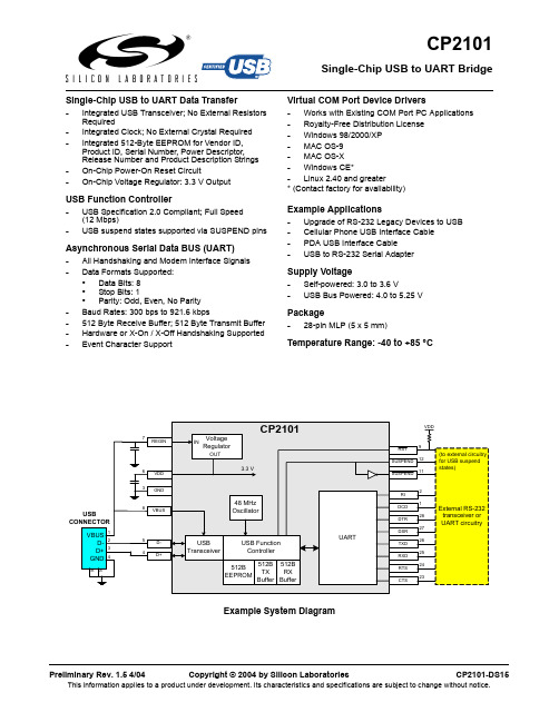
Single-Chip USB to UART BridgeCP2101Single-Chip USB to UART Data Transfer-Integrated USB Transceiver; No External Resistors Required-Integrated Clock; No External Crystal Required -Integrated 512-Byte EEPROM for Vendor ID, Product ID, Serial Number, Power Descriptor, Release Number and Product Description Strings -On-Chip Power-On Reset Circuit-On-Chip Voltage Regulator: 3.3 V OutputUSB Function Controller-USB Specification 2.0 Compliant; Full Speed (12 Mbps)-USB suspend states supported via SUSPEND pinsAsynchronous Serial Data BUS (UART)-All Handshaking and Modem Interface Signals -Data Formats Supported:•Data Bits: 8•Stop Bits: 1•Parity: Odd, Even, No Parity -Baud Rates: 300 bps to 921.6 kbps-512 Byte Receive Buffer; 512 Byte Transmit Buffer -Hardware or X-On / X-Off Handshaking Supported -Event Character SupportVirtual COM Port Device Drivers-Works with Existing COM Port PC Applications -Royalty-Free Distribution License -Windows 98/2000/XP -MAC OS-9-MAC OS-X -Windows CE*-Linux 2.40 and greater* (Contact factory for availability)Example Applications-Upgrade of RS-232 Legacy Devices to USB -Cellular Phone USB Interface Cable -PDA USB Interface Cable -USB to RS-232 Serial Adapter Supply Voltage-Self-powered: 3.0 to 3.6 V-USB Bus Powered: 4.0 to 5.25 V Package-28-pin MLP (5 x 5 mm)Temperature Range: -40 to +85 °CCP2101Table of Contents1.System Overview (4)2.Absolute Maximum Ratings (4)Table 2.1. Absolute Maximum Ratings (4)3.Global DC Electrical Characteristics (5)Table 3.1. Global DC Electrical Characteristics (5)Table 3.2. UART and Suspend I/O DC Electrical Characteristics (5)4.Pinout and Package Definitions (6)Table 4.1. Pin Definitions for the CP2101 (6)Figure 4.1. MLP-28 Pinout Diagram (Top View) (7)Figure 4.2. MLP-28 Package Drawing (8)Table 4.2. MLP-28 Package Dimensions (8)Figure 4.3. Typical MLP-28 Landing Diagram (9)Figure 4.4. Typical MLP-28 Solder Mask (10)B Function Controller and Transceiver (11)Figure 5.1. Typical Connection Diagram (11)6.Asynchronous Serial Data Bus (UART) Interface (12)Table 6.1. Data Formats and Baud Rates (12)7.Internal EEPROM (12)Table 7.1. Default USB Configuration Data (12)8.Virtual Com Port Device Drivers (13)9.Voltage Regulator (14)Table 9.1. Voltage Regulator Electrical Specifications (14)Figure 9.1. Configuration 1: USB Bus-Powered (14)Figure 9.2. Configuration 2: USB Self-Powered (15)Figure 9.3. Configuration 3: USB Self-Powered, Regulator Bypassed (15)1.System OverviewThe CP2101 is a highly-integrated USB-to-UART Bridge Controller providing a simple solution for updating RS-232 designs to USB using a minimum of components and PCB space. The CP2101 includes a USB 2.0 full-speed function controller, USB transceiver, oscillator, EEPROM and asynchronous serial data bus (UART) with full modem control signals in a compact 5 x 5 mm MLP-28 package. No other external USB components are required.The on-chip EEPROM may be used to customize the USB Vendor ID, Product ID, Product Description String, Power Descriptor, Device Release Number and Device Serial Number as desired for OEM applications. The EEPROM is programmed on-board via the USB allowing the programming step to be easily integrated into the product manufacturing and testing process.Royalty-free Virtual COM Port (VCP) device drivers provided by Silicon Laboratories allow a CP2101-based product to appear as a COM port to PC applications. The CP2101 UART interface implements all RS-232 signals, including control and handshaking signals, so existing system firmware does not need to be modified. In many existing RS-232 designs, all that is required to update the design from RS-232 to USB is to replace the RS-232 level-translator with the CP2101.An evaluation kit for the CP2101 (Part Number: CP2101EK) is available. It includes a CP2101-based USB-to-UART/RS-232 evaluation board, a complete set of VCP device drivers, USB and RS-232 cables, and full documentation. Contact a Silicon Labs’ sales representatives or go to to order the CP2101 Evaluation Kit.2.Absolute Maximum RatingsTable 2.1. Absolute Maximum RatingsParameter Conditions Min Typ Max Units Ambient temperature under bias–55—125°C Storage Temperature–65—150°C Voltage on any I/O Pin or RST with respect to–0.3— 5.8V GNDVoltage on V DD with respect to GND–0.3— 4.2V Maximum Total current through V DD and GND——500mA——100mA Maximum output current sunk by RST or anyI/O pinNote: stresses above those listed under “Absolute Maximum Ratings” may cause permanent damage to the device. This is a stress rating only and functional operation of the devices at those or any other condi-tions above those indicated in the operation listings of this specification is not implied. Exposure to maxi-mum rating conditions for extended periods may affect device reliability.CP21013.Global DC Electrical CharacteristicsTable 3.1. Global DC Electrical CharacteristicsV DD = 2.7 to 3.6 V, –40 to +85 °C unless otherwise specifiedParameter Conditions Min Typ Max Units Supply Voltage 3.0 3.3 3.6V Supply Current V DD = 3.3 V—25—mA Supply Current in Suspend V DD = 3.3 V—325—µA Specified Operating Temperature Range–40—+85°CTable 3.2. UART and Suspend I/O DC Electrical CharacteristicsV DD = 2.7 to 3.6 V, -40 to +85 °C unless otherwise specifiedParameters Conditions Min Typ Max UNITSOutput High Voltage I OH = -3mAI OH = -10µAI OH = -10mAVDD-0.7VDD-0.1VDD-0.8VOutput Low Voltage I OL = 8.5mAI OL = 10µAI OL = 25mA 1.00.60.1VInput High Voltage 2.0V Input Low Voltage0.8V Input Leakage Current2550µACP21014.Pinout and Package DefinitionsTable 4.1. Pin Definitions for the CP2101Name Pin #Type DescriptionV DD6Power InPowerOut3.0–3.6 V Power Supply Voltage Input.3.3 V Voltage Regulator Output. See Section 9.GND3GroundRST9 D I/O Device Reset. Open-drain output of internal POR or V DD monitor. An external source can initiate a system reset by driving this pin low for at least 15 µs.REGIN7Power In 5 V Regulator Input. This pin is the input to the on-chip voltage regu-lator.VBUS8 D In VBUS Sense Input. This pin should be connected to the VBUS signal of a USB network. A 5 V signal on this pin indicates a USB network connection.D+4 D I/O USB D+D–5 D I/O USB D–TXD26 D Out Asynchronous data output (UART Transmit) RXD25 D In Asynchronous data input (UART Receive) CTS23* D In Clear To Send control input (active low)RTS24* D Out Ready to Send control output (active low)DSR27* D in Data Set Ready control input (active low)DTR28* D Out Data Terminal Ready control output (active low) DCD1* D In Data Carrier Detect control input (active low)RI2* D In Ring Indicator control input (active low)SUSPEND12* D Out This pin is driven high when the CP2101 enters the USB suspend state.SUSPEND11* D Out This pin is driven low when the CP2101 enters the USB suspend state.NC10, 13–22These pins should be left unconnected or tied to V DD. *Note: Pins can be left unconnected when not used.CP2101Figure 4.1. MLP-28 Pinout Diagram (Top View)CP2101Figure 4.2. MLP-28 Package DrawingTable 0.1. MLP-28 Package DimensionsMM MIN TYP MAX A 0.800.90 1.00A100.020.05A200.65 1.00A3—0.25—b 0.180.230.30D — 5.00—D2 2.90 3.15 3.35E — 5.00—E2 2.90 3.15 3.35e —0.5—L 0.450.550.65N —28—ND —7—NE —7—R 0.09——AA —0.435—BB —0.435—CC —0.18—DD—0.18—CP2101Figure 4.3. Typical MLP-28 Landing DiagramCP2101Figure 4.4. Typical MLP-28 Solder Mask11Rev. 1.5B Function Controller and TransceiverThe Universal Serial Bus function controller in the CP2101 is a USB 2.0 compliant full-speed device with integrated transceiver and on-chip matching and pull-up resistors. The USB function controller manages all data transfers between the USB and the UART as well as command requests generated by the USB host controller and commands for controlling the function of the UART.The USB Suspend and Resume signals are supported for power management of both the CP2101 device as well as external circuitry. The CP2101 will enter Suspend mode when Suspend signaling is detected on the bus. On entering Suspend mode, the CP2101 asserts the SUSPEND and SUSPEND signals. SUSPEND and SUSPEND are also asserted after a CP2101 reset until device configuration during USB Enumeration is completeThe CP2101 exits the Suspend mode when any of the following occur: (1) Resume signaling is detected or generated, (2) a USB Reset signal is detected, or (3) a device reset occurs. On exit of Suspend mode, the SUSPEND and SUSPEND signals are de-asserted.Both SUSPEND and SUSPEND temporarily float high during a CP2101 reset. If this behavior is undesirable, a strong pulldown (10 kΩ) can be used to ensure SUSPEND remains low during reset. See Figure 5.1 for other recommended options.Figure 5.1. Typical Connection DiagramRev. 1.5126.Asynchronous Serial Data Bus (UART) InterfaceThe CP2101 UART interface consists of the TX (transmit) and RX (receive) data signals as well as the RTS, CTS, DSR, DTR, DCD and RI control signals. The UART supports RTS/CTS, DSR/DTR and X-On/X-Off handshaking.The UART is programmable to support a variety of data formats and baud rates. The data format and baud rate programmed into the UART is set during COM port configuration on the PC. The data formats and baud rates available are listed in Table 6.1.7.Internal EEPROMThe CP2101 includes an internal EEPROM that may be used to customize the USB Vendor ID, Product ID, Product Description String, Power Descriptor, Device Release Number and Device Serial Number as desired for OEM applications. Customization of the USB configuration data is optional. If the EEPROM is not programmed with OEM data, the default configuration data shown in Table 7.1 is used. However, a unique serial number is required for OEM applications in which it is possible for multiple CP2101-based devices to be connected to the same PC.The internal EEPROM is programmed via the USB. This allows the OEM's USB configuration data and serial number to be written to the CP2101 on-board during the manufacturing and testing process. A stand-alone utility for programming the internal EEPROM is available from Silicon Laboratories. A library of routines provided in the form of a Windows ® DLL is also available. This library can be used to integrate the EEPROM programming step into custom software used by the OEM to streamline testing and serial number management during manufacturing. The EEPROM has a typical endurance of 100,000 write cycles with a data retention of 100 years.Table 6.1. Data Formats and Baud RatesData Bits 8Stop Bits 1Parity Type None, Even, OddBaud Rates300, 600, 1200, 1800, 2400, 4800, 7200, 9600, 14400, 19200, 28800, 38400, 56000, 57600, 115200, 128000, 230400, 460800, 921600Table 7.1. Default USB Configuration DataName Value Vendor ID 10C4h Product IDEA60h Power Descriptor (Attributes)80hPower Descriptor (Max. Power)32h Release Number 0100hSerial Number0001 (63 characters maximum)Product Description String“CP2101 USB to UART Bridge Controller” (126 characters maximum)13Rev. 1.58.Virtual Com Port Device DriversThe CP2101 Virtual COM Port (VCP) device drivers allow a CP2101-based device to appear to the PC's application software as an additional COM port (in addition to any existing hardware COM ports). Application software running on the PC accesses the CP2101-based device as it would access a standard hardware COM port. However, actual data transfer between the PC and the CP2101 device is performed over the USB. Therefore, existing COM port applications may be used to transfer data via the USB to the CP2101-based device without modifying the application. Contact Silicon Laboratories for the latest list of supported operating systems.Note:The Silicon Laboratories VCP device drivers are required for device operation and are only distributed as part of the CP2101 Evaluation Kit (Part Number: CP2101EK). Contact any of Silicon Lab’s sales representatives or go to to order the CP2101 Evaluation Kit. The CP2101 drivers and programming utilities are subject to change without notice. Subscription to the website "Auto Email Alert" system for automatic notification of updates and the use of the "Product Update Registration" service is recommended.Rev. 1.5149.Voltage RegulatorThe CP2101 includes an on-chip 5-to-3 V voltage regulator. This allows the CP2101 to be configured as either a USB bus-powered device or a USB self-powered device. These configurations are shown in Figure 9.1 and Figure 9.2. When enabled, the 3 V voltage regulator output appears on the V DD pin and can be used to power external 3V devices. See Table 9.1 for the voltage regulator electrical characteristics.Alternatively, if 3 V power is supplied to the V DD pin, the CP2101 can function as a USB self-powered device with the voltage regulator disabled. For this configuration, it is recommended that the REGIN input be tied to the 3 V net to disable the voltage regulator. This configuration is shown in Figure 9.3.The USB max power and power attributes descriptor must match the device power usage and configuration. See application note “AN144: CP2101 Customization Guide” for information on how to customize USB descriptors for the CP2101.Note:It is recommended that additional decoupling capacitance (e.g., 0.1 µF in parallel with 1.0 µF) be provided on the REGIN input.Figure 9.1. Configuration 1: USB Bus-PoweredTable 9.1. Voltage Regulator Electrical Specifications–40 to +85 °C unless otherwise specifiedParameterConditionsMin Typ Max Units Input Voltage Range 4.0— 5.25V Output VoltageOutput Current = 1 to 100 mA*3.0 3.3 3.6V VBUS Detection Input Threshold 1.0 1.84.0V Bias Current—90TBDµA* The maximum regulator supply current is 100 mA.15Rev. 1.5Figure 9.2. Configuration 2: USB Self-PoweredFigure 9.3. Configuration 3: USB Self-Powered, Regulator BypassedRev. 1.516Document Change ListRevision 1.4 to Revision 1.5Updated Example System Diagram on page 1.Updated Table 3.1, “Global DC Electrical Characteristics,” on page 5.Added Table 3.2, “UART and Suspend I/O DC Electrical Characteristics,” on page 5 Added Table note to Table 4.1, “Pin Definitions for the CP2101,” on page 6 Added Figure 5.1. , "Typical Connection Diagram" on page 11Removed asterisk from the “Linux 2.40 and greater” bullet on page 117Rev. 1.5NotesRev. 1.518Contact InformationSilicon Laboratories Inc.4635 Boston Lane Austin, TX 78735Tel: 1+(512) 416-8500 Fax: 1+(512) 416-9669 Toll Free: 1+(877) 444-3032Email:********************** Internet: Silicon Laboratories and Silicon Labs are trademarks of Silicon Laboratories Inc.Other products or brandnames mentioned herein are trademarks or registered trademarks of their respective holdersThe information in this document is believed to be accurate in all respects at the time of publication but is subject to change without notice. Silicon Laboratories assumes no responsibility for errors and omissions, and disclaims responsibility for any consequences resulting from the use of information included herein. Additionally, Silicon Laboratories assumes no responsibility for the function-ing of undescribed features or parameters. Silicon Laboratories reserves the right to make changes without further notice. Silicon Laboratories makes no warranty, representation or guarantee regarding the suitability of its products for any particular purpose, nor does Silicon Laboratories assume any liability arising out of the application or use of any product or circuit, and specifically disclaims any and all liability, including without limitation consequential or incidental damages. Silicon Laboratories products are not designed, intended, or authorized for use in applications intended to support or sustain life, or for any other application in which the failure of the Silicon Laboratories product could create a situation where personal injury or death may occur. Should Buyer purchase or use Silicon Laboratories products for any such unintended or unauthorized application, Buyer shall indemnify and hold Silicon Laboratories harmless against all claims and damages.。
温控仪中英文对照

干式变压器温度控制仪Temperature Controller for Dry-type Transformer安装使用说明书Installation Operation Instruction辽宁金立电力电器有限公司LIAO NING JIN LI ELECTRIC POWER EQUIPMENT CO.,LTDNO.1在使用您所购置的温控仪之前,请务必仔细阅读我公司的使用说明书。
并妥善保管,以备使用中查阅。
By all means please carefully read the operation instruction of our company before using the temperature controller. And please keep it safely for reference.注意事项 Note☆ 本说明书由最终使用者保留!☆ The manual should be kept by the end users!☆ 安装操作前,请认真阅读本手册!☆ Please carefully read the manual before installation and operation!☆ ※在进行变压器耐压试验前应先将传感电缆插头与温控仪分离,以免损坏温控仪!!!☆ ※Separate the sensor cable plug and temperature controller before havingwithstand voltage test of transformer in order to avoid damage☆ 为让温控仪能够长时间稳定运行,在搬运、安装时尽可能小心轻放。
☆ Please be careful as much as possible when handling and installing in order that the temperature controller can have a long and stable operation.☆ 请勿将温控仪安装在高温、强腐蚀性、高场强的环境当中。
SA2532K资料

AN1500A
PDS038-SA2532K-001
Rev. C
21-03-00
元器件交易网
AN1500A
TABLE OF CONTENTS
1 2 3 4 5 6 7
SCOPE................................................................................................................................................................. 1 KEY FEATURES ................................................................................................................................................. 1 OTHER APPLICABLE DOCUMENTS AND PAPERS ........................................................................................ 4 REVISION STATUS............................................................................................................................................. 4 SA2532K PIN LAYOUT . ..................................................................................................................................... 4 GENERAL DESCRIPTION .................................................................................................................................. 5 DEMO BOARD CONFIGURATION..................................................................................................................... 5
广州唯创电子有限公司 WTN4 系列语音芯片说明书

广州唯创电子有限公司MP3录音模块WTN4系列语音芯片说明书3I/O Single-Chip Speech SynthesizerV1.052017-01-17Note:WAYTRONIC ELECTRONIC CO.,LTD.reserves the right to change this document without prior rmation provided by WAYTRONIC is believed to be accurate and reliable.However,WAYTRONIC makes no warranty for any errors which may appear in this document.Contact WAYTRONIC to obtain the latest version of device specifications before placing your orders.No responsibility is assumed by WAYTRONIC for any infringement of patent or other rights of third parties which may result from its use.In addition,WAYTRONIC products are not authorized for use as critical components in life support devices/systems or aviation devices/systems,where a malfunction or failure of the product may reasonably be expected to result in significant injury to the user, without the express written approval of WAYTRONIC.目录1、概述: (3)2、功能简述: (3)3、管脚描述: (4)3.1、WTN4045/WTN4065/WTN4105-8S管脚介绍 (4)3.2、WTN4165-8S管脚介绍 (4)3.3、极限参数: (5)3.4、直流特性: (5)4、一线串口通讯: (6)4.1、管脚分配: (6)4.2、一线语音地址对应关系: (6)4.3、一线语音及命令码对应表: (7)4.4、一线串口时序图: (7)4.5、一线串口程序范例: (8)5、两线串口通讯: (9)5.1、管脚分配: (9)5.2、语音地址对应关系: (9)5.3、语音及命令码对应表: (9)5.4、两线串口时序图: (10)5.5、两线串口程序范例: (10)6、数脉冲控制方式: (11)6.1、管脚分配: (11)6.2、语音地址对应关系: (11)6.3、数脉冲控制时序: (12)6.4、数脉冲程序范例: (12)7、应用电路: (13)7.1、WTN4045/065/105-8S一线串口控制应用电路 (13)7.2、WTN4045/065/105-8S两线串口控制应用电路 (14)7.3、WTN4045/065/105-8S数脉冲控制应用电路 (14)7.4、WTN4165-8S一线串口控制应用电路 (15)7.5、WTN4165-8S两线串口控制应用电路 (15)7.6、WTN4165-8S数脉冲控制应用电路 (16)8、管脚封装图: (16)9、版本记录 (17)1、概述WTN4系列语音芯片是广州唯创电子有限公司推出的一系列语音芯片,其性能优越,价格实惠。
外文翻译--基于51单片机温度报警器的设计(适用于毕业论文外文翻译+中英文对照)

外文翻译--基于51单片机温度报警器的设计(适用于毕业论文外文翻译+中英文对照)XXX: Design of a Temperature Alarm Based on 51 MCUDepartment: n EngineeringMajor: Measurement and Control Technology and nClass:Student ID:Name:Supervisor:Date:A microcontroller。
also known as a single-chip computer system。
XXX its ns being integrated on a small chip。
it has most of the components needed for a complete computer system。
such as CPU。
memory。
internal and external bus systems。
and mostof them also have external storage。
At the same time。
it integrates XXX interfaces。
timers。
real-time clocks。
etc。
The most XXX integrate sound。
image。
ork。
and complex input-output systems on a single chip.XXX used in the industrial control field。
Microcontrollers XXX CPUs inside the chip。
The original design concept was to integrate a large number of peripheral devices and CPUs on a chip to make the computer system XXX's Z80 was the first processor designed according to this concept。