DTC114技术资料
IBMX60笔记本电路图_GAOQS

就爱技术网 Wistron CorporationKS NoteSBBlock Diagram533/667MHzAGTL+ FSBIntel ICH7-MUSB 2.0 (2+2+2+2)LAN Connect I/F (LCI)AC97 2.3/Azalia InterfaceUltra ATA/100/66/33ACPI 2.0INT. RTCLPC I/F PCI Rev 2.3L7:GNDL3:Signal 1System DC/DCVINT19L4:VCC L8:ComponentL1:Component OUTPUTSL6:Signal 3L2:GND PCB Layer StackupINPUTSMAX1977L5:Signal 2July 22 '05VCC3MVCC5M Battery Charger/SelectorMAX8724DOCK_PWR19_FM-BAT-PWR VINT19ADP3207CPU DC/DCVCCCPUCORE3,4,58,9,10,11,12,13,14596564Yonah NV/LV/ULV IntelIntel Calistoga-GMLVDS INTEGRATED GRAHPICSDDR2 400/533/667MHz DMI x4CK-410MClock Generator 47,48H8S/2161BKBCLPC Bus / 33MHz12.1'' XGA LCDLVDS2021RGB CRTCRT SELECTIONSD Socket34PCMCIA SLOT +USB-based NEW Card3331,32Power Switch RICOH R5C5841Cardbus +SD Card +IEEE1394R5534VSUPER I/O PC873825143SST-49LF008FWHLPC Debug Board Conn43TCPA Chip5450PMH-7G/ASerial ATA I/FUSB 2.0AC97 CODEC AD1981HDHP OUTOP AMP MAX9750MDC 423027,28,29Modem ATA 66/100IDE I/F Port 0Int. MICMIC INKS Note Block Diagram46Media Slice VCC1R05B/VCC1R5MS-BAT-PWRUSB x 4HDD, Optical DrivesCRT HP OUT Parallel PortRJ11DC-INUltraBay46RJ452nd BatteryStereo Speaker x 2Media SliceMIC INMAX3243RS232 Transceiver52TFDU6102FIRPC87392NS SIO COM Port LPC BusUSB20H04USB HubSMSC MAX1989LM75Thermal SensorSMBusIDE I/F23,24,25,2622CRT PortMedia Slice 46535405207-SB-FINALProcessor 19Serial ATA 150MB/sPCI Express CRT I/FG-Sensor5635CH5Finger Print45CH7DDR2 400/533/667Channel A UNBUFFERED DDR2 SODIMM Reverse Socket200-PIN DDR SODIMM1516Channel B DDR2 400/533/667VCC1R8AVINT19VINT19VCC1R8MVCC1R5M VCC1R05BMAX1540MAX86326768I2C Bus / SM Bus ThermalSensor LM265UNBUFFERED DDR2 SODIMM Normal SocketIEEE1394CONN31MediaBay I/FPCI Bus / 33MHzWWAN Card41Mini PCI-E 36,37IntelGBE TEKOA WLAN Card41Mini PCI-EPCI ExpressUSB 2.0 CH282573MPCI Express ATMELAT25010AN 3938GBE Switch PI3L500ZFEX Media Slice46RJ45Conn40454545AC LINKPCMCIA I/FUSB 2.0 CH3CH0,1,4USB 3USB 1USB 2Bus Switch ICCH6Bluetooth 2049Int. KB Track point IV44Board toBoard CONNSATA HDDKeyboard Light^_^ReferenceDYYONAH CPU(1/3)YONAH CPU(2/3)YONAH CPU(3/3)CALISTOGA(1/7):HOST I/FCALISTOGA(2/7):DDR2-ACALISTOGA(3/7):DDR2-BCALISTOGA(4/7):DMI/PM/CFGCALISTOGA(6/7):VCCCALISTOGA(7/7):GNDDDR-2 TERMINATIONDYCLOCK GEN(CK410M)就爱技术网 DYLCD CONNECTORCRT SELECTOREXT CRT INTERFACE就爱技术网 DYICH7-M(1/4):PCI/PCIE/DMI/USB/SPI就爱技术网 ICH7-M(2/4):ATA/AC97/LPCICH7-M(3/4):PM/SMB/GPIOICH7-M(4/4):VCC/GNDAUDIO AD1981HDJSTZ2 2 2AUDIO AMP MAX9750CARD BUS CONTROLLER(1/2)CARD BUS CONTROLLER(2/2)CARD BUS SLOT2 2 22 2 2CARD BUS POWER CONTROLGBE VIDALIA (1/2)GBE VIDALIA (2/2) : POWERGBE LAN SW就爱技术网 DYGBE MAGNETICS15MINI CARD SLOT22DYMH2AMP-CONN12A-1GPFWH, RTC BATTERY就爱技术网 USB POWER / CONNECTORSLICE CONNECTOR就爱技术网 KEYBOARD CONN。
tc114 通用数据要求标准

标题:TC114 通用数据要求标准摘要:TC114是指ISO/TC 114国际标准化技术委员会,该委员会制定了一系列通用数据要求标准,涵盖了多个领域,为提高数据交换和共享的效率和准确性提供了重要的支持。
本文将对TC114的通用数据要求标准进行介绍和分析,探讨其在实际应用中的意义和影响。
一、TC114 的背景和作用ISO/TC 114国际标准化技术委员会成立于1996年,是一个负责制定钢铁、铁合金和有色金属材料的国际标准的专业委员会。
在其领域内,TC114致力于制定通用数据要求标准,旨在提高数据的交换和共享效率,确保各类材料数据的准确性和可靠性。
二、TC114 的通用数据要求标准分类TC114的通用数据要求标准主要分为以下几类:1. 数据格式标准:包括数据的编码、格式、结构等方面的要求,以确保数据能够在不同系统和评台之间进行有效地交换和共享。
2. 数据质量标准:包括数据的准确性、完整性、一致性等方面的要求,以确保数据能够满足特定的使用需求。
3. 数据安全标准:包括数据的保护、权限控制、加密等方面的要求,以确保数据在传输和存储过程中不受到未经授权的访问和篡改。
4. 数据管理标准:包括数据的采集、存储、检索、更新等方面的要求,以确保数据能够有效地管理和利用。
三、TC114 的通用数据要求标准的应用TC114的通用数据要求标准在各个领域得到了广泛的应用,包括但不限于材料科学、工程设计、生产制造、供应链管理等。
在材料科学领域,TC114的标准为各类材料的数据交换和共享提供了基础支持,促进了材料研发和应用的进步。
在工程设计领域,TC114的标准为设计数据的交换和共享提供了便利,促进了设计效率和精度的提高。
在生产制造领域,TC114的标准为生产过程中的数据管理和控制提供了指导,促进了生产效率和质量的提升。
在供应链管理领域,TC114的标准为供应链上下游之间的数据交换和共享提供了规范,促进了供应链的协同和响应能力的提升。
DTC114YET1G中文资料
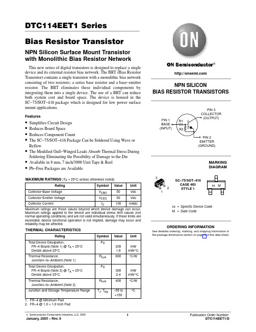
DTC114EET1 SeriesBias Resistor TransistorNPN Silicon Surface Mount Transistor with Monolithic Bias Resistor Network This new series of digital transistors is designed to replace a single device and its external resistor bias network. The BRT (Bias Resistor Transistor) contains a single transistor with a monolithic bias network consisting of two resistors; a series base resistor and a base−emitter resistor. The BRT eliminates these individual components by integrating them into a single device. The use of a BRT can reduce both system cost and board space. The device is housed in the SC−75/SOT−416 package which is designed for low power surface mount applications.Features•Simplifies Circuit Design•Reduces Board Space•Reduces Component Count•The SC−75/SOT−416 Package Can be Soldered Using Wave or Reflow•The Modified Gull−Winged Leads Absorb Thermal Stress During Soldering Eliminating the Possibility of Damage to the Die •Available in 8 mm, 7 inch/3000 Unit Tape & Reel•Pb−Free Packages are AvailableMAXIMUM RATINGS(T= 25°C unless otherwise noted)Maximum ratings applied to the device are individual stress limit values (not normal operating conditions) and are not valid simultaneously. If these limits are exceeded, device functional operation is not implied, damage may occur and reliability may be affected.THERMAL CHARACTERISTICS2.FR−4 @ 1.0 × 1.0 Inch PadNPN SILICONBIAS RESISTOR TRANSISTORSSC−75/SOT−416CASE 463STYLE 121PIN 3(OUTPUT)PIN 2EMITTER(GROUND)PIN 1BASExx= Specific Device CodeM=Date CodeMARKINGDIAGRAMSee detailed ordering, marking, and shipping information in the package dimensions section on page 2 of this data sheet.ORDERING INFORMATION†For information on tape and reel specifications, including part orientation and tape sizes, please refer to our Tape and Reel Packaging Specifications Brochure, BRD8011/D.ELECTRICAL CHARACTERISTICS(T= 25°C unless otherwise noted)ON CHARACTERISTICS (Note 3)3.Pulse Test: Pulse Width < 300 m s, Duty Cycle < 2.0%ELECTRICAL CHARACTERISTICS (T A = 25°C unless otherwise noted) (Continued)Figure 1. Derating Curve250200150100500T A , AMBIENT TEMPERATURE (°C)P D , P O W E R D I S S I P A T I O N (M I L L I W A T T S )0.0010.010.11.0r (t ), N O R M A L I Z E D T R A N S I E N T T H E R M A L R E S I S T A N C Et, TIME (s)Figure 2. Normalized Thermal ResponseV i n , I N P U T V O L T A G E (V O L T S )I C , C O L L E C T O R C U R R E N T (m A )h F E , D C C U R R E N T G A I N (N O R M A L I Z E D )Figure 3. V CE(sat) versus I CI C , COLLECTOR CURRENT (mA)1010.1Figure 4. DC Current GainFigure 5. Output Capacitance 10.10.010.001I C , COLLECTOR CURRENT (mA)V C E (s a t ), M A X I M U M C O L L E C T O R V O L T A G E (V O L T S )100010010I C , COLLECTOR CURRENT (mA)Figure 6. Output Current versus Input VoltageV in , INPUT VOLTAGE (VOLTS)Figure 7. Input Voltage versus Output Current4312V R , REVERSE BIAS VOLTAGE (VOLTS)C o b , C A P A C I T A N C E (p F )I C , COLLECTOR CURRENT (mA)Figure 12. Input Voltage versus OutputCurrent0.001V C E (s a t ), M A X I M U M C O L L E C T O R V O L T A G E (V O L T 0.010.1143210C o b , C A P A C I T A N C E (p F )V i n , I N P U T V O L T A G E (V O L T S )V in , INPUT VOLTAGE (VOLTS)Figure 15. Output Capacitance I C , COLLECTOR CURRENT (mA)Figure 16. Output Current versus Input Voltage10.80.60.40.20V R , REVERSE BIAS VOLTAGE (VOLTS)C o b , C A P A C I T A N C E (p F )Figure 17. Input Voltage versus Output Current1010.10.01V C E (s a t ), M A X I M U M C O L L E C T O R V O L T A G E (V O L T1010.143.532.521.510.50V R , REVERSE BIAS VOLTAGE (VOLTS)V i n , I N P U T V O L T A G E (V O L T S )V C E (s a t ), M A X I M U M C O L L E C T O R V O L T A G E (V O L T S )Figure 20. Output Capacitance Figure 21. Output Current versus Input VoltageV in , INPUT VOLTAGE (VOLTS)C o b , C A P A C I T A N C E (p F )Figure 22. Input Voltage versus Output CurrentI C , COLLECTOR CURRENT (mA)10.10.010.001TYPICAL APPLICATIONS FOR NPN BRTsFigure 23. Level Shifter: Connects 12 or 24 Volt Circuits to LogicFigure 25. Inexpensive, Unregulated Current Source Figure 24. Open Collector Inverter:Inverts the Input SignalPACKAGE DIMENSIONSSC−75/SOT−416CASE 463−01ISSUE Cǒmm inchesǓSCALE 10:1*For additional information on our Pb−Free strategy and solderingdetails, please download the ON Semiconductor Soldering and Mounting Techniques Reference Manual, SOLDERRM/D.SOLDERING FOOTPRINT*ON Semiconductor and are registered trademarks of Semiconductor Components Industries, LLC (SCILLC). SCILLC reserves the right to make changes without further notice to any products herein. SCILLC makes no warranty, representation or guarantee regarding the suitability of its products for any particular purpose, nor does SCILLC assume any liability arising out of the application or use of any product or circuit, and specifically disclaims any and all liability, including without limitation special, consequential or incidental damages.“Typical” parameters which may be provided in SCILLC data sheets and/or specifications can and do vary in different applications and actual performance may vary over time. All operating parameters, including “Typicals” must be validated for each customer application by customer’s technical experts. SCILLC does not convey any license under its patent rights nor the rights of others. SCILLC products are not designed, intended, or authorized for use as components in systems intended for surgical implant into the body, or other applications intended to support or sustain life, or for any other application in which the failure of the SCILLC product could create a situation where personal injury or death may occur. Should Buyer purchase or use SCILLC products for any such unintended or unauthorized application, Buyer shall indemnify and hold SCILLC and its officers, employees, subsidiaries, affiliates,and distributors harmless against all claims, costs, damages, and expenses, and reasonable attorney fees arising out of, directly or indirectly, any claim of personal injury or death associated with such unintended or unauthorized use, even if such claim alleges that SCILLC was negligent regarding the design or manufacture of the part. SCILLC is an Equal Opportunity/Affirmative Action Employer. This literature is subject to all applicable copyright laws and is not for resale in any manner.PUBLICATION ORDERING INFORMATION。
DTC114WCA中文资料
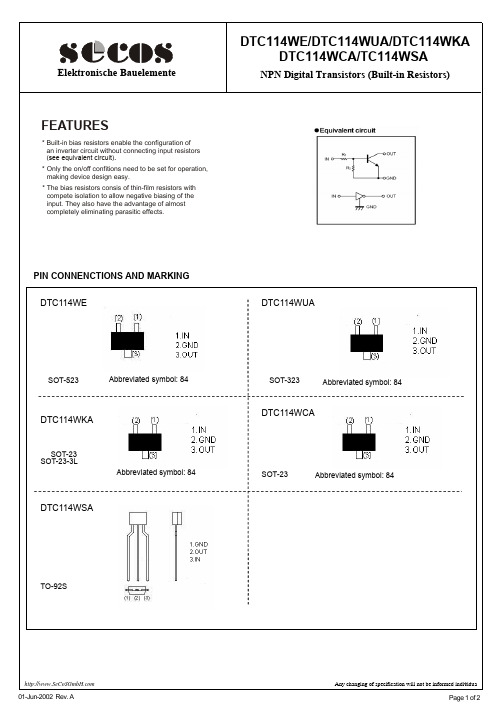
DTC114WE/DTC114WUA/DTC114WKA DTC114WCA/TC114WSA
NPN Digital Transistors (Built-in Resistors)
Absolute maximum ratings (Ta=25℃)
Parameter Supply voltage Input voltage Output current Power dissipation Junction temperature Storage temperature
Elektronische Bauelemente
DTC114WE/DTC114WUA/DTC114WKA DTC114WCA/TC114WSA
NPN Digital Transistors (Built-in Resistors)
FEATURES
* Built-in bias resistors enable the configuration of an inverter circuit without connecting input resistors (see equivalent circuit). * Only the on/off confitions need to be set for operation, making device design easy. * The bias resistors consis of thin-film resistors with compete isolation to allow negative biasing of the input. They also have the advantage of almost completely eliminating parasitic effects.
军用EMC标准CS114试验方法的演变和改进探讨
平台
2.4 CS114 监测电流限值
9 无 曲线 3 曲线 3 曲线 3 曲线 3 空间系统
பைடு நூலகம்
CS114 最大监测电流限值在不同的标准版本中 也有变化袁 如表 3 所示 遥 [1-9]
3 MIL-STD-461G 中 CS114 测试方法 变化探讨
3.1 校准配置变化
校准配置变化袁 将监测探头加入到校准测试 中袁 如图 1 所示遥 目的是将监测探头对环路阻抗 的影响纳入校准测试中袁 与测试配置保持一致袁 提供更加精准的前向功率数据遥
10 无 11 无 12 无
曲线 3 曲线 4 曲线 4 曲线 3 曲线 5 曲线 5 曲线 5 曲线 5 曲线 5
曲线 4 陆军地面 无 海军飞机
曲线 5 飞机外部等
3.2 检定配置方法
检定测试获得的监测电流频率与幅度曲线应 该与目标校准限值一致遥 该方法简单尧 巧妙地闭 环验证了 CS114 测试校准的准确性 遥 [11]
Discussion on Evolution and Improvement of CS114 Test Method of Military EMC Standard
XIONG Yiming袁 GUO Huadong袁 CHEN Siyang
渊Beijing Institute of Astronautical Systems Engineering袁 Beijing 100076袁 China冤
CS114 测试方法尧 测试对象尧 校准限值频率和幅度尧 监测电流限值的变化及原因遥 总结了海陆空天各种平台的 EMC 限值要求袁 并建议减少限值数量袁 建立面向联合作战体系的统一限值遥
关键词院 军用标准曰 CS114曰 电磁兼容曰 试验方法曰 传导敏感度曰 大电流注入 中图分类号院 T-651曰 T-652 文献标志码院 A 文章编号院 1672-5468 渊2021冤 03-0075-06 doi:10.3969/j.issn.1672-5468.2021.03.014
omron C200H-CP114凸轮定位器单元 说明书

前面:原点修正,动作模式切换 后面:旋转方向切换,设定/解除凸轮数据保护,可/不可调整运转
DC5V 0.3A以下
DC24V
+10% -15%
2A以上
34.5(W)×130(H)×101(D)mm
350g
⬉ᄤ⏽఼ 各部位的名称和功能
᭄ᄫ䴶ᵓ㸼 ●各部位的名称
˄㸼䴶˅
ൟোؐ
ᡔᴃᣛफ
LEDᰒ冫 ADJᓔ݇ (ॳ⚍ׂℷ⫼)
᭄䆒ᅮࠊЁᖗ C200H-DSC01
䕧ߎ䆒
I/O㒻⬉఼㒜ッ G7TC-OC16 G70D-SOC16 G70D-FOM16
种类
名称
本体
凸轮定位器单元
数据设定控制中心
连接电缆
解析器
轴φ10 轴φ6
标准型 高转矩型 连接器型 导线型
解析器延长电缆 (带两个连接器)
RS15用解析器电缆 (带两个连接器)
䚼ߌ䕂䕧ߎ ᦦӊ
ᑩതऩܗ 䖲ᦦӊ
1472 凸轮定位器单元 C200H-CP114
外形尺寸
●凸轮定位器单元 重量 :350g
130
安装尺寸
(单位 :mm)
ᑩ ത ऩ ܗ
34.5
●凸轮定位器单元 重量 :120g
101
11
㑺200
96
91
48
12
45
44Biblioteka 357面板孔加工尺寸
安装尺寸
92+00.8
RS15W用解析器电缆 (带单连接器)
凸轮输出用
I/O继电器终端 继电器终端
推荐电缆
型号 C200H-CP114 C200H-DSC01 2m C200H-CN225 4m C200H-CN425 3F88L-RS17 3F88L-RS17T 3F88L-RS15 3F88L-RS15W 2m 3F88L-CR002C 5m 3F88L-CR005C 10m 3F88L-CR010C 20m 3F88L-CR020C 3m 3F88L-CR003NA 5m 3F88L-CR005NA 10m 3F88L-CR010NA 15m 3F88L-CR015NA 20m 3F88L-CR020NA 3m 3F88L-CR003SA 5m 3F88L-CR005SA 10m 3F88L-CR010SA G7TC-OC16 G7VC-OC16 G7VC-OA16 G7VC-OD16 1m G79-100C 1.5m G79-150C 2m G79-200C 3m G79-300C 5m G79-500C
DDTC114YUA中文资料
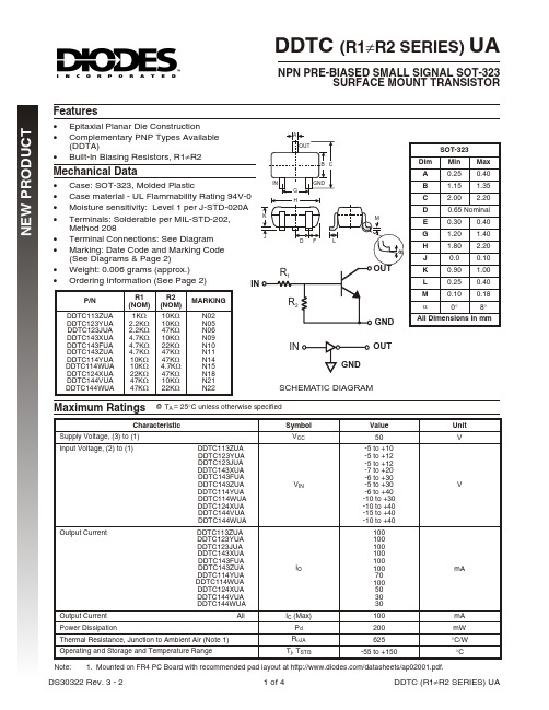
Notes: 2. For Packaging Details, go to our website at /datasheets/ap02007.pdf.
DS30322 Rev. 3 - 2
2 of 4
DDTC (R1¹R2 SERIES) UA
元器件交易网 Marking Information
(DDTA) · Built-In Biasing Resistors, R1¹R2
Mechanical Data
A OUT
BC
· Case: SOT-323, Molded Plastic · Case material - UL Flammability Rating 94V-0 · Moisture sensitivity: Level 1 per J-STD-020A
元器件交易网
DDTC (R1¹R2 SERIES) UA
NPN PRE-BIASED SMALL SIGNAL SOT-323 SURFACE MOUNT TRANSISTOR
NEW PRODUCT
Features
· Epitaxial Planar Die Construction · Complementary PNP Types Available
Tj, TSTG
Value
50
-5 to +10 -5 to +12 -5 to +12 -7 to +20 -6 to +30 -5 to +30 -6 to +40 -10 to +30 -10 to +40 -15 to +40 -10 to +40
100 100 100 100 100 100 70 100 50 30 30
和记奥普泰传输产品技术建议书

和记奥普泰传输产品技术建议书目录第一章综述 (3)第二章和记奥普泰SDH光传输系统 (5)§2.1概述 (5)§2.2遵循的ITU-T建议和国标 (6)§2.3OPS-155/622/2500系统特点 (7)§2.3.1 OPS-155 (7)§2.3.2 OPS-622 (9)§2.3.3 OPS-2500..................................................................错误!未定义书签。
§2.4机械结构和工艺. (10)§2.4.1 机械结构 (10)§2.4.2 工艺 (11)§2.5环境要求§2.6机房土建要求§2.7接地保护系统 (11)§2.8机架结构 (13)§2.8.1 OPS-155/622子架排列 (13)§2.8.2 OPS-2500子架 (15)§2.9保护倒换机制 (15)§2.9.1 设备级单元保护 ......................................................错误!未定义书签。
§2.9.2 网络级业务保护 (15)§2.10组网应用 (16)§2.10.1 点对点 (16)§2.10.2 链路应用 (16)§2.10.3 环网应用 (17)§2.10.4 环网链路混合应用 (17)§2.10.5 两环间交叉连接应用 (18)§2.10.6 复杂组网应用示例 (18)§2.11网管系统 (19)第三章组网方案 (21)§3.1组网方案 (21)§3.2组网方案说明 (21)第四章设备板位图及配置清单 (21)§4.1×××××站点 (21)第五章工程界面图 (22)第六章说明 (23)§6.1保证条款 (23)§6.2培训计划 (23)第一章综述当今电信网络正朝着数字化、宽带化、综合化、智能化和个人化的方向发展。
- 1、下载文档前请自行甄别文档内容的完整性,平台不提供额外的编辑、内容补充、找答案等附加服务。
- 2、"仅部分预览"的文档,不可在线预览部分如存在完整性等问题,可反馈申请退款(可完整预览的文档不适用该条件!)。
- 3、如文档侵犯您的权益,请联系客服反馈,我们会尽快为您处理(人工客服工作时间:9:00-18:30)。
NPN SILICON BIAS RESISTOR TRANSISTORS
COLLECTOR
3
1
BASE
2
EMITTER
3
2
1
CASE 463
SOT–416/SC–75
STYLE 1
Thermal Clad is a trademark of the Bergquist Company
ON Semiconductor and are trademarks of Semiconductor Components Industries, LLC (SCILLC). SCILLC reserves the right to make changes without further notice to any products herein. SCILLC makes no warranty, representation or guarantee regarding the suitability of its products for any particular purpose, nor does SCILLC assume any liability arising out of the application or use of any product or circuit, and specifically disclaims any and all liability, including without limitation special, consequential or incidental damages. “Typical” parameters which may be provided in SCILLC data sheets and/or specifications can and do vary in different applications and actual performance may vary over time. All operating parameters, including “Typicals” must be validated for each customer application by customer’s technical experts. SCILLC does not convey any license under its patent rights nor the rights of others.
SCILLC products are not designed, intended, or authorized for use as components in systems intended for surgical implant into the body, or other applications intended to support or sustain life, or for any other application in which the failure of the SCILLC product could create a situation where personal injury or death may occur. Should Buyer purchase or use SCILLC products for any such unintended or unauthorized application, Buyer shall indemnify and hold SCILLC and its officers, employees, subsidiaries, affiliates, and distributors harmless against all claims, costs, damages, and expenses, and reasonable attorney fees arising out of, directly or indirectly, any claim of personal injury or death associated with such unintended or unauthorized use, even if such claim alleges that SCILLC was negligent regarding the design or manufacture of the part. SCILLC is an Equal Opportunity/Affirmative Action Employer. PUBLICATION ORDERING INFORMATION
CENTRAL/SOUTH AMERICA:
Spanish Phone:303–308–7143 (Mon–Fri 8:00am to 5:00pm MST)
Email:ONlit–spanish@
ASIA/PACIFIC: LDC for ON Semiconductor – Asia Support
Phone:303–675–2121 (Tue–Fri 9:00am to 1:00pm, Hong Kong Time)
Toll Free from Hong Kong & Singapore:
001–800–4422–3781
Email: ONlit–asia@
JAPAN: ON Semiconductor, Japan Customer Focus Center
4–32–1 Nishi–Gotanda, Shinagawa–ku, Tokyo, Japan 141–0031
Phone: 81–3–5740–2745
Email: r14525@。