11SM601-H4;中文规格书,Datasheet资料
MW6S004NT1;中文规格书,Datasheet资料

RF Power Field Effect TransistorN-Channel Enhancement-Mode Lateral MOSFETDesigned for Class A or Class AB base station applications with frequencies up to 2000 MHz. Suitable for analog and digital modulation and multicarrier amplifier applications.•Typical Two-Tone Performance @ 1960 MHz, 28 Volts, I DQ = 50 mA, P out = 4 Watts PEP Power Gain — 18 dB Drain Efficiency — 33%IMD — -34 dBc•Typical Two-Tone Performance @ 900 MHz, 28 Volts, I DQ = 50 mA, P out = 4 Watts PEP Power Gain — 19 dB Drain Efficiency — 33%IMD — -39 dBc•Capable of Handling 5:1 VSWR, @ 28 Vdc, 1960 MHz, 4 Watts CW Output Power Features•Characterized with Series Equivalent Large-Signal Impedance Parameters •On-Chip RF Feedback for Broadband Stability •Integrated ESD Protection •RoHS Compliant•In Tape and Reel. T1 Suffix = 1000 Units per 12 mm, 7 inch Reel.Table 1. Maximum RatingsRatingSymbol Value Unit Drain-Source Voltage V DSS -0.5, +68Vdc Gate-Source Voltage V GS -0.5, +12Vdc Storage Temperature Range T stg -65 to +150°C Operating Junction TemperatureT J150°CTable 2. Thermal CharacteristicsCharacteristicSymbol Value (1,2)Unit Thermal Resistance, Junction to CaseCase Temperature 76°C, 4 W PEP , Two-Tone Case Temperature 79°C, 4 W CWR θJC8.88.5°C/WTable 3. ESD Protection CharacteristicsTest MethodologyClass Human Body Model (per JESD22-A114)1C (Minimum)Machine Model (per EIA/JESD22-A115) A (Minimum)Charge Device Model (per JESD22-C101)IV (Minimum)1.MTTF calculator available at /rf. Select Software & Tools/Development Tools/Calculators to access MTTF calculators by product.2.Refer to AN1955, Thermal Measurement Methodology of RF Power Amplifiers. Go to /rf. Select Documentation/Application Notes - AN1955.Document Number: MW6S004NRev. 4, 6/2009Freescale Semiconductor Technical DataMW6S004NT1Table 4. Moisture Sensitivity LevelTest MethodologyRating Package Peak TemperatureUnit Per JESD 22-A113, IPC/JEDEC J-STD-0203260°CTable 5. Electrical Characteristics (T A = 25°C unless otherwise noted)CharacteristicSymbolMinTypMaxUnitOff CharacteristicsZero Gate Voltage Drain Leakage Current (V DS = 68 Vdc, V GS = 0 Vdc)I DSS ——10μAdc Zero Gate Voltage Drain Leakage Current (V DS = 28 Vdc, V GS = 0 Vdc)I DSS ——10μAdc Gate-Source Leakage Current (V GS = 5 Vdc, V DS = 0 Vdc)I GSS——500nAdcOn CharacteristicsGate Threshold Voltage(V DS = 10 Vdc, I D = 50 mAdc)V GS(th) 1.22 2.7Vdc Gate Quiescent Voltage(V DS = 28 Vdc, I D = 50 mAdc)V GS(Q)— 2.7—Vdc Fixture Gate Quiescent Voltage (1)(V DD = 28 Vdc, I D = 50 mAdc, Measured in Functional Test)V GG(Q) 2.23 4.2Vdc Drain-Source On-Voltage(V GS = 10 Vdc, I D = 50 mAdc)V DS(on)—0.270.37VdcDynamic CharacteristicsReverse Transfer Capacitance(V DS = 28 Vdc ± 30 mV(rms)ac @ 1 MHz, V GS = 0 Vdc)C rss —21—pF Output Capacitance(V DS = 28 Vdc ± 30 mV(rms)ac @ 1 MHz, V GS = 0 Vdc)C oss —25—pF Input Capacitance(V DS = 28 Vdc, V GS = 0 Vdc ± 30 mV(rms)ac @ 1 MHz)C iss—30—pFFunctional Tests (In Freescale Test Fixture, 50 ohm system) V DD = 28 Vdc, I DQ = 50 mA, P out = 4 W PEP , f1 = 1960 MHz, f2 = 1960.1 MHz, Two-Tone Test Power Gain G ps 16.51820dB Drain EfficiencyηD 2833—%Intermodulation Distortion IMD —-34-28dBc Input Return LossIRL—-12-10dBTypical Performance (In Freescale 900 MHz Demo Board, 50 ohm system) V DD = 28 Vdc, I DQ = 50 mA, P out = 4 W PEP , f = 900 MHz, Two-Tone Test, 100 kHz Tone Spacing Power Gain G ps —19—dB Drain EfficiencyηD —33—%Intermodulation Distortion IMD —-39—dBc Input Return LossIRL—-12—dB1.V GG = 11/10 x V GS(Q). Parameter measured on Freescale Test Fixture, due to resistive divider network on the board. Refer to Test Circuit Schematic.MW6S004NT1Figure 1. MW6S004NT1 Test Circuit SchematicZ70.210″ x 1.220″ Microstrip Z80.054″ x 0.680″ Microstrip Z90.054″ x 0.260″ Microstrip Z100.025″ x 0.930″ MicrostripPCBArlon CuClad 250GX-0300-55-22, 0.020″, εr = 2.5Z10.054″ x 0.430″ Microstrip Z20.054″ x 0.137″ Microstrip Z30.580″ x 0.420″ Microstrip Z40.580″ x 0.100″ Microstrip Z50.025″ x 0.680″ Microstrip Z60.210″ x 0.100″ MicrostripV SUPPLYTable 6. MW6S004NT1 Test Circuit Component Designations and ValuesPartDescriptionPart Number Manufacturer C1100 nF Chip Capacitor CDR33BX104AKYS Kemet C2, C3, C6, C79.1 pF Chip Capacitors ATC100B9R1CT500XT ATC C4, C510 μF, 50 V Chip Capacitors GRM55DR61H106KA88B Murata C810 μF, 35 V Tantalum Chip Capacitor T490D106K035AT Kemet R1 1 k Ω, 1/4 W Chip Resistor CRCW12061001FKEA Vishay R210 k Ω, 1/4 W Chip Resistor CRCW12061002FKEA Vishay R310 Ω, 1/4 W Chip ResistorCRCW120610R0FKEAVishayMW6S004NT1Figure 2. MW6S004NT1 Test Circuit Component LayoutMW6S004NT1TYPICAL CHARACTERISTICS1420191716G p s , P O W E R G A I N (d B )100.1TWO−TONE SPACING (MHz)1100Figure 6. Intermodulation Distortion Productsversus Tone Spacing 26P in , INPUT POWER (dBm)1618222414Figure 7. Pulsed CW Output Power versusInput PowerI M D , I N T E R M O D U L A T I O N D I S T O R T I O N (d B c )181520MW6S004NT1TYPICAL CHARACTERISTICSA C P R (dB )−70P out , OUTPUT POWER (WATTS) AVG.50−2040−3030−4020−5010−600.01110Figure 8. Single-Carrier CDMA ACPR, Power Gainand Drain Efficiency versus Output PowerP out , OUTPUT POWER (WATTS) CWFigure 10. Power Gain versus Output Power 7151906171618234G p s , P O W E R G A I N (d B )1800−250f, FREQUENCY (MHz)Figure 11. Broadband Frequency Response−5−10−15−20210020502000195019001850S 11 (d B )851ηD , D R A I N E F F I C I E N C Y (%), G p s , P O W E R G A I N (d B )0.118.517.516.515.5MW6S004NT1TYPICAL CHARACTERISTICS25010790T J , JUNCTION TEMPERATURE (°C)Figure 12. MTTF versus Junction TemperatureThis above graph displays calculated MTTF in hours when the device is operated at V DD = 28 Vdc, P out = 4 W PEP, and ηD = 33%.MTTF calculator available at /rf. Select Software & Tools/Development Tools/Calculators to access MTTF calculators by product.106105104110130150170190M T T F (H O U R S )210230MW6S004NT1f = 1930 MHzZ o = 10 ΩZ loadZ sourcef = 1990 MHzf = 1930 MHzf = 1990 MHzV DD = 28 Vdc, I DQ = 50 mA, P out = 4 W PEPfMHzZ sourceWZ loadW1930 1.96 - j5.348.78 + j6.961960 1.89 - j5.108.93 + j7.461990 1.82 - j4.859.11 + j7.97Z source=Test circuit impedance as measured fromgate to ground.Z load=Test circuit impedance as measured fromdrain to ground.Z source Z loadOutputMatchingNetworkFigure 13. Series Equivalent Source and Load ImpedanceMW6S004NT1Table 7. Common Source Scattering Parameters (V DD = 28 V, 50 ohm system)I DQ = 50 mAf MH S 11S 21S 12S 22MHz |S 11|∠φ|S 21|∠φ|S 12|∠φ|S 22|∠φ5000.649-116.3407.902105.4200.056-73.7500.548-33.5705500.695-121.6807.50298.7900.053-80.5700.593-41.4806000.733-126.5607.11192.3800.049-87.0100.632-48.8906500.770-131.340 6.69986.2900.045-93.2800.669-56.0007000.800-135.740 6.30280.4500.041-99.1200.701-62.8107500.827-140.030 5.92274.8500.038-104.8500.727-69.2908000.848-143.950 5.55269.6300.035-110.1100.750-75.3508500.866-147.690 5.22064.5800.032-115.2200.770-81.1309000.882-151.140 4.89159.9700.029-119.9600.786-86.5709500.895-154.560 4.59755.4900.026-124.7900.800-91.73010000.907-157.590 4.31551.2400.024-129.0900.813-96.66010500.916-160.540 4.06047.1700.022-133.3700.824-101.34011000.923-163.310 3.81943.3400.020-137.4600.833-105.79011500.929-165.930 3.60139.6500.018-141.4400.840-110.05012000.935-168.430 3.39836.1100.017-145.3300.847-114.17012500.938-170.770 3.21032.7400.015-149.5400.851-118.06013000.942-173.030 3.03629.4900.014-153.4300.856-121.88013500.945-175.140 2.87526.3600.013-157.4600.859-125.52014000.948-177.170 2.72823.3300.012-161.9100.863-129.02014500.951-179.090 2.59020.4400.011-166.1800.866-132.39015000.953179.030 2.46417.6400.010-170.6300.869-135.65015500.954177.270 2.34714.9200.009-174.8900.872-138.76016000.955175.570 2.24012.3200.008179.9500.875-141.75016500.956173.980 2.1399.7400.008173.9200.877-144.65017000.957172.350 2.0477.2500.007167.7100.880-147.48017500.957170.800 1.958 4.8100.007161.8100.882-150.18018000.958169.340 1.879 2.4400.006155.3700.884-152.76018500.959167.920 1.8060.2600.006148.9400.886-155.23019000.959166.510 1.736-1.9800.005142.6300.887-157.58019500.960165.200 1.668-4.3100.005136.7400.888-160.05020000.959163.800 1.611-6.2400.005129.9100.890-162.07020500.959162.420 1.555-8.2900.005123.8100.891-164.19021000.958161.170 1.504-10.2700.005118.2000.892-166.14021500.958159.840 1.456-12.2100.005112.7400.893-168.06022000.957158.560 1.412-14.1300.005108.4600.894-169.84022500.957157.160 1.372-16.0100.005103.8400.896-171.61023000.955155.870 1.334-17.8700.00599.3100.896-173.26023500.954154.510 1.300-19.7000.00595.3600.897-174.83024000.953153.120 1.268-21.5100.00591.0300.898-176.39024500.953151.7301.238-23.2500.00587.4600.899-177.840MW6S004NT1Table 7. Common Source Scattering Parameters (V DD = 28 V, 50 ohm system) (continued)I DQ = 50 mAf MH S 11S 21S 12S 22MHz |S 11|∠φ|S 21|∠φ|S 12|∠φ|S 22|∠φ25000.952150.340 1.211-25.1200.00684.1600.899-179.27025500.950149.010 1.187-26.9200.00680.7800.897179.42026000.949147.380 1.166-28.6500.00677.8800.897178.12026500.948145.920 1.144-30.4200.00774.6700.898176.84027000.944144.200 1.121-32.3100.00771.3600.896175.48027500.944142.790 1.105-34.2300.00767.9800.897174.06028000.943141.020 1.088-36.0000.00763.9500.897172.93028500.941139.410 1.073-37.8700.00761.2300.896171.63029000.940137.640 1.058-39.7600.00859.8100.896170.33029500.938135.900 1.045-41.6800.00858.2800.896169.04030000.937133.8601.032-43.6100.00856.7400.895167.510分销商库存信息: FREESCALEMW6S004NT1。
SD51;中文规格书,Datasheet资料

Major Ratings and Characteristics SCHOTTKY RECTIFIER60 AmpSD51Bulletin PD-2.327 rev. C 11/02TO-203AB (DO-5)SD512Bulletin PD-2.327 rev. C 11/02T J Max. Junction Temperature Range -65 to 150°C T stgMax. Storage Temperature Range-65 to 150°C R thJC Max. Thermal Resistance Junction1.0°C/W DC o peration * See Fig. 4to Case R thCS Typical Thermal Resistance, Case to0.25°C/WMounting surface , smooth and greasedHeatsink wt Approximate Weight 15 (0.53)g (oz.)TMounting T orque Min.23 (20)Non-lubricated t hreads Max.46 (40)Case S tyleDO-203AB(DO-5)JEDECKg-cm (Ibf-in)Thermal-Mechanical SpecificationsParametersSD51UnitsConditionsV FMMax. Forward Voltage Drop (2)0.58V @ 35A * See Fig. 10.66V @ 60A 0.86V @ 120A 0.75V @ 120A I RM Max. Reverse Leakage Current (2)50mA T J = 25 °C * See Fig. 2200mA T J = 125 °CC T Max. Junction Capacitance 2900pF V R = 5V DC , (test signal range 100Khz to 1Mhz) 25 °C L STypical Series Inductance7.5nH Measured from top of terminal to mounting planedv/dt Max. Voltage Rate of Change10000V/ µs(Rated V R )V R = rated V RElectrical SpecificationsParametersSD51UnitsConditions(2) Pulse Width < 300µs, Duty Cycle < 2%T J = 150 °C T J = 25 °C I F(AV)Max. Average Forward Current60A 50% duty cycle @ T C = 90°C, rectangular wave form * See Fig. 5I FSMMax. Peak One Cycle Non-Repetitive 800A60Hz half cycle sine wave Surge Current * See Fig. 7or 5ms rectangular pulseParametersSD51 UnitsConditionsAbsolute Maximum RatingsFollowing any rated load condition and with rated V RRM appliedPart numberSD51V RMax. DC Reverse Voltage (V)V RWM Max. Working Peak Reverse Voltage (V)45(1)Voltage Ratings* For Additional Informations and Graphs, Please See the 50HQ Series(1) For SD51 V RWM and V RRM = 45V @ T J = 25°C , =35V @ T J = 150°CSD513Bulletin PD-2.327 rev. C 11/02SD514Bulletin PD-2.327 rev. C 11/024812160102030405060708090A l l o w a b l e C a s e T e m p e r a t u r e - (°C )A v e r a g e F o r w a r d C u r r e n t - I (A )F (A V)5101520253004080120160200A v e r a g e P o w e r L o s s - (W a t t s )F (A V )A v e r a g e F o r w a r d C u r r e n t - I (A )Fig. 5 - Maximum Allovable Case TemperatureVs. Average Forward CurrentFig. 6 - Forward Power Loss Characteristics10100100010100100010000pF S MN o n -R e p e t i t i v e S u r g e C u r r e n t - I (A )S q u a r e W a v e P u l s e D u r a t i o n - t (m i c r o s e c )Fig. 7 - Max. Non-Repetitive Surge CurrentIR WORLD HEADQUARTERS: 233 Kansas St., El Segundo, California 90245, USA Tel: (310) 252-7105TAC Fax: (310) 252-7309Visit us at for sales contact information. 11/02Data and specifications subject to change without notice.This product has been designed for Industrial Level.Qualification Standards can be found on IR's Web site.分销商库存信息: VISHAYSD51。
DMN601TK-7;中文规格书,Datasheet资料
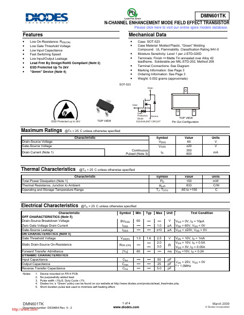
Features• Low On-Resistance: R DS(ON) • Low Gate Threshold Voltage • Low Input Capacitance • Fast Switching Speed• Low Input/Output Leakage• Lead Free By Design/RoHS Compliant (Note 2) • ESD Protected Up To 2kV • "Green" Device (Note 4)Mechanical Data• Case: SOT-523 • Case Material: Molded Plastic, “Green” MoldingCompound. UL Flammability Classification Rating 94V-0 • Moisture Sensitivity: Level 1 per J-STD-020D • Terminals: Finish ⎯ Matte Tin annealed over Alloy 42leadframe. Solderable per MIL-STD-202, Method 208 • Terminal Connections: See Diagram • Marking Information: See Page 3 • Ordering Information: See Page 3 • Weight: 0.002 grams (approximate)Maximum Ratings @T A = 25°C unless otherwise specifiedCharacteristicSymbol Value Units Drain-Source Voltage V DSS 60 VGate-Source Voltage V GSS±20 V Drain Current (Note 1) ContinuousPulsed (Note 3)I D300800mAThermal Characteristics @T A = 25°C unless otherwise specifiedCharacteristicSymbol Value Units Total Power Dissipation (Note 1)P D 150 mW Thermal Resistance, Junction to Ambient R θJA 833 °C/W Operating and Storage Temperature Range T J , T STG-65 to +150°CElectrical Characteristics @T A = 25°C unless otherwise specifiedCharacteristicSymbol Min Typ Max UnitTest ConditionOFF CHARACTERISTICS (Note 5) Drain-Source Breakdown Voltage BV DSS 60 ⎯ ⎯ V V GS = 0V, I D = 10μA Zero Gate Voltage Drain Current I DSS ⎯ ⎯ 1.0 μA V DS = 60V, V GS = 0V Gate-Source LeakageI GSS ⎯ ⎯ ±10 μA V GS = ±20V, V DS = 0V ON CHARACTERISTICS (Note 5) Gate Threshold VoltageV GS(th) 1.0 1.6 2.5 VV DS = 10V, I D = 1mA Static Drain-Source On-Resistance R DS (ON) ⎯ ⎯ ⎯ 2.0 3.0 ΩV GS = 10V, I D = 0.5A V GS = 5V, I D = 0.05A Forward Transfer Admittance |Y fs | 80 ⎯ ⎯ ms V DS =10V, I D = 0.2A DYNAMIC CHARACTERISTICS Input Capacitance C iss ⎯ ⎯ 50 pF V DS = 25V, V GS = 0V f = 1.0MHz Output CapacitanceC oss ⎯ ⎯ 25 pF Reverse Transfer CapacitanceC rss⎯⎯5.0pFNotes: 1. Device mounted on FR-4 PCB. 2. No purposefully added lead.3. Pulse width ≤10μS, Duty Cycle ≤1%4. Diodes Inc.’s “Green” policy can be found on our website at /products/lead_free/index.php.5. Short duration pulse test used to minimize self-heating effect.SOT-523TOP VIEWPin Out ConfigurationESD Protected up to 2kVEQUIVALENT CIRCUITPlease click here to visit our online spice models database.V , DRAIN-SOURCE VOLTAGE (V)Fig. 1 Typical Output CharacteristicsDS I , D R A I N C U R R E N T (A )DFig. 2 Typical Transfer CharacteristicsGS T , CHANNEL TEMPERATURE (°C)Fig. 3 Gate Threshold Voltage vs. Channel T emperaturech 00.51.5I DRAIN CURRENT (A)Fig. 4 Static Drain-Source On-Resistancevs. Drain CurrentD , R , S T A T I C D R A I N -S O U R CE D S (O N)Fig. 5 Static Drain-Source On-Resistancevs. Drain CurrentDR , S T A T I C D R A I N -S O U R C E D S (O N )V GATE SOURCE VOLTAGE (V)Fig. 6 Static Drain-Source On-Resistancevs. Gate-Source VoltageGS,R , S T A T I C D R A I N -S O U R C E O N -R E S I S T A N C E ()D S (O N )ΩFig. 7 CH Static Drain-Source On-State Resistancevs. Channel T emperatureR , S T A T I C D R A I N -S O U R C E D S (O N )1I , R E V E R S E D R A I N C U R RE N T (A )D R 1I , DRAIN CURRENT (A)D Fig.10 Forward Transfer Admittancevs. Drain CurrentOrdering Information (Note 6)Part Number Case Packaging DMN601TK-7SOT-523 3000/Tape & ReelNotes: 6. For packaging details, go to our website at /datasheets/ap02007.pdf.Marking InformationDate Code KeyYear 2005 2006 2007 2008 2009 2010 2011 2012 Code S T U V W X Y ZMonth Jan Feb Mar Apr May Jun Jul Aug Sep Oct Nov Dec Code 1 2 3 4 5 6 7 8 9 O N DK7K = Product Type Marking Code YM = Date Code Marking Y = Year (ex: S = 2005) M = Month (ex: 9 = September) K7K YMPackage Outline DimensionsSuggested Pad LayoutIMPORTANT NOTICEDiodes Incorporated and its subsidiaries reserve the right to make modifications, enhancements, improvements, corrections or other changes without further notice to any product herein. Diodes Incorporated does not assume any liability arising out of the application or use of any product described herein; neither does it convey any license under its patent rights, nor the rights of others. The user of products in such applications shall assume all risks of such use and will agree to hold Diodes Incorporated and all the companies whose products are represented on our website, harmless against all damages.LIFE SUPPORTDiodes Incorporated products are not authorized for use as critical components in life support devices or systems without the expressed written approval of the President of Diodes Incorporated.SOT-523Dim Min Max Typ A 0.15 0.30 0.22 B 0.75 0.85 0.80 C 1.45 1.75 1.60 D ⎯ ⎯ 0.50 G 0.90 1.10 1.00 H 1.50 1.70 1.60 J 0.00 0.10 0.05 K 0.60 0.80 0.75 L 0.10 0.30 0.22 M 0.10 0.20 0.12 N 0.45 0.65 0.50α0° 8° ⎯ All Dimensions in mmDimensions Value (in mm)Z1.8 X 0.4 Y 0.51 C 1.3 E 0.7X EYCZ分销商库存信息: DIODESDMN601TK-7。
MIC3003GFL;MIC3003GFL TR;中文规格书,Datasheet资料

MIC3003GFLFOM Management IC with Internal CalibrationMLF and MicroLead Frame are registered trademarks of Amkor Technology, Inc.General DescriptionThe MIC3003GFL is a fiber optic module controller which enables the implementation of sophisticated, hot-pluggable fiber optic transceivers with intelligent laser control and an internally calibrated Digital Diagnostic Monitoring Interface per SFF-8472. It essentially integrates all non-data path functions of an SFP/SFP+ transceiver into a tiny (3mm x 3mm ) MLF ® package. It also works well as a microcontroller peripheral in transponders or 10Gbps transceivers. The MIC3003GFL uses the same die as the MIC3003 with all its functions, but in a smaller package and different pin out. A highly configurable automatic power control (APC) circuit controls laser bias. Bias and modulation are temperature compensated using dual DACs, an on-chip temperature sensor, and NVRAM look-up tables. A programmable internal feedback resistor provides a wide dynamic range for the APC. Controlled laser turn-on.An analog-to-digital converter converts the measured temperature, voltage, bias current, transmit power, and received power from analog to digital. An EEPOT provides front-end adjustment of RX power. Each parameter is compared against user-programmed warning and alarm thresholds. Analog comparators and DACs provide fast monitoring of received power and critical laser operating parameters. Data can be reported as either internally calibrated or externally calibrated.An interrupt output, power-on hour meter, and data-ready bits add user friendliness beyond SFF-8472. The interrupt output and data-ready bits reduce overhead in the host system. The power-on hour meter logs operating hours using an internal real-time clock and stores the result in NVRAM.In addition to the features listed above, the MIC3003 features an extended temperature range, options to mask alarms and warnings interrupt and TXFAULT, a reset signal source, and the ability to support up to four chips with the same address on the serial interface. It also supports eight-byte SMBus block writes.Communication with the MIC3003 is via an industry standard 2-wire SMBus serial interface. Nonvolatile memory is provided for serial ID, configuration, and separate OEM and user scratchpad spaces.Datasheets and support documentation can be found on Micrel’s web site at: .Features• Packaged in a ultra small (3mm x 3mm) 24-pin MLF ® package • Extended temperature range• Alarms and warnings interrupt and TXFAULT masks • Capability to support up to four devices on one SMBus • APC or constant-current laser bias• Turbo mode for APC loop start-up and shorter laser turn on time • Supports multiple laser types and bias circuit topologies • Integrated digital temperature sensor• Temperature compensation of modulation, bias, bias fault and alarm thresholds via NVRAM look-up tables • NVRAM to support GBIC/SFP serial ID function • User writable EEPROM scratchpad• Reset signal compatible with some new systems requirements • Diagnostic monitoring interface per SFF-8472 – Monitors and reports critical parameters:temperature, bias current, TX and RX optical power, and supply voltage– S/W control and monitoring of TXFAULT, RXLOS, RATESELECT, and TXDISABLE – Internal or external calibration– EEPOT for adjusting RX power measurement • Power-on hour meter • Interrupt capability• Extensive test and calibration features • 2-wire SMBus-compatible serial interface • SFP/SFP+ MSA and SFF-8472 compliant • 3.0V to 3.6V power supply range • 5V-tolerant I/OApplications• SFP/SFP+ optical transceivers• SONET/SDH transceivers and transponders • Fibre Channel transceivers • 10Gbps transceivers• Free space optical communications • Proprietary optical linksTypical ApplicationOrdering InformationPart NumberPackage Marking Junction Temp.RangePackage Type Lead FinishMIC3003GFL GFL 3003 with Pb-Free bar-line indicator–45°C to +105°C24-pin (3mm x 3mm) MLF ® Pb-Free,NiPdAuMIC3003GFLTR (1) GFL 3003 with Pb-Free bar-line indicator–45°C to +105°C24-pin (3mm x 3mm) MLF ® Pb-Free,NiPdAuNote:1. Tape and Reel.ContentsGeneral Description (1)Features (1)Pin Configuration (8)Pin Configuration (8)Pin Description (MIC3003GFL only) (8)Absolute Maximum Ratings (10)Operating Ratings (10)Electrical Characteristics (10)Electrical Characteristics (12)Electrical Characteristics (13)Serial Interface Timing Diagram (14)Serial Interface Address Maps (15)Block Diagram (18)Analog-to-Digital Converter/Signal Monitoring (18)Alarms and Warnings Interrupt Source Masking (19)Alarms and Warnings as TXFAULT Source (21)Latching of Alarms and Warnings (21)SMBus Multipart Support (21)QGOP Pin Function (21)Calibration Modes (22)A/ External Calibration (22)Voltage (22)Temperature (22)Bias Current (22)TX Power (22)RX Power (23)B/ Internal Calibration (23)Computing Internal Calibration Results (23)C/ Reading the ADC Result Registers (25)RXPOT (25)Laser Diode Bias Control (25)Laser Modulation Control (26)Power On and Laser Start-Up (27)Fault Comparators (28)SHDN and TXFIN (29)Temperature Measurement (30)Diode Faults (30)Temperature Compensation (30)Alarms and Warning Flags (32)Control and Status I/O (32)System Timing (34)Warm Resets (36)Power-On Hour Meter (36)Test and Calibration Features (37)Serial Port Operation (38)Block Writes (38)Acknowledge Polling (39)Write Protection and Data Security (39)OEM Password (39)OEM Mode and User Mode (39)Detailed Register Descriptions (40)Alarm Threshold Registers (40)Temperature High Alarm Threshold (40)Temperature Low Alarm Threshold (40)Voltage High Alarm Threshold (40)D[7] read/write (40)Bias Current High Alarm Threshold (41)Bias Current Low Alarm Threshold (41)TX Optical Power High Alarm Threshold (41)TX Optical Power Low Alarm Threshold (42)RX Optical Power High Alarm Threshold (42)RX Optical Power Low Alarm Threshold (42)Warning Threshold Registers (43)Temperature High Warning Threshold (43)Temperature Low Warning Threshold (43)Voltage High Warning Threshold (43)Voltage Low Warning Threshold (44)Bias Current High Warning Threshold (44)Bias Current Low Warning Threshold (44)TX Optical Power High Warning (44)TX Optical Power Low Warning (45)RX Optical Power High Warning Threshold (45)RX Optical Power Low Warning Threshold (45)Checksum (CHKSUM) Checksum of bytes 0 - 94 at serial address A2h (45)ADC Result Registers (46)Temperature Result (46)Voltage (46)Laser Diode Bias Current (46)Transmitted Optical Power (47)Received Optical Power (47)Control and Status (CNTRL) (47)Application Select Control Mode (ASCM) (48)Alarm Flags (50)Alarm Status Register 0 (ALARM0) (50)Alarm Status Register 1 (ALARM1) (50)Warning Flags (51)Warning Status Register 0 (WARN0) (51)Warning Status Register 1 (WARN1) (51)Extended Control and Status (ECNTRL) (52)OEM Password Entry (OEMPW) (52)Power-On Hours (POHh and POHl) (53)Data Ready Flags (DATARDY) (53)User Control Register (USRCTL) (54)RESETOUT (54)OEM Configuration Register 0 (OEMCFG0) (55)OEM Configuration Register 1 (OEMCFG1) (56)OEM Configuration Register 2 (OEMCFG2) (57)APC Setpoint 0, 1, and 2 (APCSET0, APCSET1, APCSET2) Automatic Power Control Setpoint (58)Modulation Setpoint 0, 1, and 2 (MODSET0, MODSET1, and MODSET2) Nominal V MOD Setpoint (58)I BIAS Fault Threshold (IBFLT) Bias Current Fault Threshold (59)Transmit Power Fault Threshold (TXFLT) (59)Loss-Of-Signal Threshold (LOSFLT) (59)Fault Suppression Timer (FLTTMR) Fault Suppression Interval in Increments of 0.5 ms (60)Fault Mask (FLTMSK) (60)OEM Password Setting (OEMPWSET) (61)OEM Calibration 0 (OEMCAL0) (61)OEM Calibration 1 (OEMCAL1) (63)LUT Index (LUTINDX) (64)OEM Configuration 3 (OEMCFG3) (64)BIAS DAC Setting (APCDAC) Current VBIAS Setting (65)Modulation DAC Setting (MODDAC) Current VMOD Setting (66)OEM Readback Register (OEMRD) (66)OEM Configuration 4 (OEMCFG4) (67)OEM Configuration 5 (OEMCFG5) (68)OEM Configuration 6 (OEMCFG6) (69)Power-On Hour Meter Data (POHDATA) (70)OEM Scratchpad Registers (SCRATCHn) (71)RX Power Coefficient Look-up Table (RXLUTn) (71)Calibration Constants (CALCOEFn) (72)Manufacturer ID Register (MFG_ID) Identifies Micrel as the manufacturer of the device. Always returns 2Ah (72)Device ID Register (DEV_ID) (73)Package Information (74)Figure 1. MIC3003 Block Diagram (18)Figure 2. Analog-to-Digital Converter Block Diagram (18)Figure 3. Internal Calibration RX Power Linear Approximation (25)Figure 4. RXPOT Block Diagram (25)Figure 5. APC and Modulation Control Block Diagram (26)Figure 6. Programmable Feedback Resistor (26)Figure 7. Transmitter Configurations Supported by MIC3003 (26)Figure 8. V MOD Configured as Voltage Output with Gain (27)Figure 9. MIC3003 Power-On Timing (OE = 1) (28)Figure 10. Fault Comparator Logic (28)Figure 11. Saturation Detector (29)Figure 12. RXLOS Comparator Logic (29)Figure 14. Transmitter On-Off Timing (34)Figure 15. Initialization Timing with TXDISABLE Asserted (34)Figure 16. Initialization Timing with TXDISABLE Not Asserted (34)Figure 17. Loss-of-Signal (LOS) Timing (35)Figure 19. Successfully Clearing a Fault Condition (36)Figure 20. Unsuccessful Attempt to Clear a Fault (36)Figure 21. Write Byte Protocol (38)Figure 22. Read Byte Protocol (38)Figure 23. Read_Word Protocol (38)Figure 24. Eight-Byte Block Write Protocol (39)Table 1. Serial Interface Address Map, Device Address = A0h (15)Table 2. Serial Interface Address Map, Device Address = A2 (15)Table 3. Serial Interface Address Map (Temperature Compensation Tables), Device Address = A4h (16)Table 4. Serial Interface Address Map (OEM Configuration Registers), Device Address = A6h (17)Table 5. A/D Input Signal Ranges and Resolutions (19)Table 6. V AUX Input Signal Ranges and Resolutions (19)Table 7. Alarms Interrupt Sources Masking Bits (20)Table 8. Warnings Interrupt Sources Masking Bits (20)Table 9. RESETOUT Clear Delay (21)Table 10. LSB Values of Offset Coefficients (23)Table 11. Internal Calibration Coefficient Memory Map – Part I (24)Table 12. Internal Calibration Coefficient Memory Map – Part II (24)Table 13. Shutdown State of SHDN vs. Configuration Bits (27)Table 14. Shutdown State of V BIAS vs. Configuration Bits (27)Table 15. Shutdown State of V MOD vs. Configuration Bits (27)Table 16. Temperature Compensation Look-up Tables (30)Table 17. APC Temperature Compensation Look-Up Table (31)Table 18. I MOD Temperature Compensation Look-Up Table (31)Table 19. I BIAS Comparator Temperature Compensation Look-Up Table (31)Table 20. BIAS Current High Alarm Temperature Compensation Table (31)Table 21. MIC3003 Alarm and Warning Events (33)Table 22. Test and Diagnostic Features (37)Pin Configuration24-Pin MLF® (ML)Pin Description (MIC3003GFL only)Pin Number Pin Name Pin Function1 VDDD Power supply input for digital functions.Open-drain output. Can be selected (via OEMCFG3 bit 7) to be an open-drain GPO or an active-2 QGPOlow, open-drain, pulsed reset signal output controlled by the status of bits [0-2] of byte A2h: FFh.3 GNDD Ground return for digital functions.Digital input. Receiver Rate Select input. OR’ed with soft rate select bit SRS0 to determine the4 RS0state of the RRSOUT pin. The state of this pin is always reflected in the RS0S bit.If bit 4 (IE) in the USRCTL register is set to 0 (its default value), this pin is configured as an analog5 VIN/INTinput. If IE bit is set to 1, this pin is configured as an open-drain output.Analog input: Multiplexed A/D input for monitoring supply voltage, with a 0V to 5.5V input range.Open-drain output: outputs the internally generated active-low interrupt signal /INT.6 CLK Digital input. Serial clock input.7 DATA Digital I/O, open-drain, bi-directional serial data input/output.Digital input; Active high. The transmitter is disabled when this input is high or the STXDIS bit is8 TXDISABLEset to 1. The state of this input is always reflected in the TXDIS bit.Digital Output; Open-Drain, with programmable polarity. If OEMCFG5 bit 4 is set to 0, a high level9 TXFAULTindicates a hardware fault impeding transmitter operation. If OEMCFG5 bit 4 is set to 1, a low levelindicates a hardware fault impeding transmitter operation. The state of this pin is always reflectedin the TXFLT bit.Digital Input; Transmitter Rate Select Input; OR’ed with soft rate select bit SRS1 to determine the10 RS1state of the TRSOUT pin. The state of this pin is always reflected in the RS1S bit.Analog Input. Multiplexed A/D converter input for monitoring received optical power. The input11 VRXrange is 0 to V REF. A 5-bit programmable EEPOT on this pin provides coarse calibration andranging of the RX power measurement.Pin Number Pin Name Pin Function12 SHDN/TXFINDigital output/Input; programmable polarity. When used as shutdown output (SHDN), OEMCFG3bit 2 set to 0, SHDN is asserted at the detection of a fault condition if OEMCFG4 bit 7 is set to 0. IfOEMCFG4 bit 7 is set to 1, a fault condition will not assert SHDN. When programmed as TXFIN, itis an input for external fault signals to be OR’ed with the internal fault sources to drive TXFAULT.13 VILD+Analog Input. Multiplexed A/D input for monitoring laser bias current via a sense resistor (signalinput); accommodates inputs referenced to V DD or GND (see pin 14 description).14 VILD–Analog Input. Reference terminal for the multiplexed pseudo-differential A/D converter inputs formonitoring laser bias current via a sense resistor (VILD+ is the sensing input). Tie to V DD or GNDto reference the voltage sensed on VILD+ to V DD or GND, respectively.15 VDDA Power supply input for analog functions.16 GNDA Ground return for analog functions.17 VMPDAnalog Input. Multiplexed A/D converter input for monitoring transmitted optical power via amonitor photodiode. In most applications, VMPD will be connected directly to FB. The input rangeis 0 - V REF or 0 - V REF/4 depending upon the setting of the APC configuration bits18 FBAnalog Input. Feedback voltage for the APC loop op-amp. Polarity and scale are programmablevia the APC configuration bits I OEMCFG1. Connect to V BIAS if APC is not used.19 VMODAnalog Output. Buffered DAC output to set the modulation current on the laser driver IC. Operateswith either a 0– V REF or a (V DD–V REF) – V DD output swing so as to generate either a ground-referenced or a V DD referenced programmed voltage. A simple external circuit can be used togenerate a programmable current for those drivers that require a current rather than a voltageinput.20 VMOD–Analog input. This pin is the inverting terminal of the VMOD buffer op-amp. Connect to VMOD(gain = 1) or a feedback resistor network to set a different gain value.21 VBIASAnalog output. Buffered DAC output capable of sourcing or sinking up to 10mA under control ofthe APC function to drive an external transistor or the APCSET pin of a laser diode driver for laserdiode DC bias. The output and feedback polarity are programmable to accommodate either anNPN or a PNP transistor to drive a common-anode or common-cathode laser diode.22 COMPAnalog output. Compensation terminal for the APC loop. Connect a capacitor between this pin andGNDA or V DDA with the appropriate value to tune the APC loop time constant to a desirable value.23 RRSOUT/GPO Digital Output. Open-Drain or push-pull.If OEMCFG3 bit 4 is set to 0, RRSOUT is selected. It represents the receiver rate select as per SFF. This output is controlled by the SRS0 bit OR’ed with RS0 input and is open drain only.If OEMCFG3 bit 4 is set to 1, GPO is selected. General-purpose, non-volatile output, it is controlled by the GPO configuration bits in OEMCFG3.24 RXLOS/TRSOUT Digital output. This programmable polarity, open-drain outputs has two purposes:If OEMCFG6 bit 2 = 0, indicates the loss of the received signal as indicated by a level of received optical power below the programmed RXLOS comparator threshold; may be wire-OR’ed with external signals. Normal operation is indicated by a low level when OEMCFG6 bit 3 is set to 0 and a high level when OEMCFG6 bit 3 is set to 1. RXLOS is de-asserted when VRX > LOSFLTn. The LOS bit reflects the state of RXLOS whether driven by the MIC3003 or an external circuit.If OEMCFG6 bit 2 = 1, TRSOUT is selected. This signal represents the transmitter rate select as per the SFF specification. This output is controlled by the SRS1 bit OR’ed with the RS1 input.Absolute Maximum Ratings(1)Power Supply Voltage, V DD.......................................+3.8V Voltage on CLK, DATA, TXFAULT, VIN, RXLOS, TXDISABLE, RS0, RS1.........................–0.3V to +6.0V Voltage On Any Other Pin.....................–0.3V to V DD+0.3V Power Dissipation, T A = 85°C....................................1.5W Junction Temperature (T J).......................................150°C Storage Temperature (T S).......................–65°C to +150°C Soldering (20 sec.)...................................................260ºC ESD Ratings(3)Human Body Model..................................................2kV Machine Model.......................................................300V Operating Ratings(2)Power Supply Voltage, V DDA/V DDD...........+3.0V to +3.6V Ambient Temperature Range (T A) .......–40°C to +105°C Package Thermal ResistanceMLF® (θJA).................................................60°C/WElectrical CharacteristicsFor typical values, T A = 25°C, V DDA = V DDD = +3.3V, unless otherwise noted. Bold values are guaranteed for +3.0V ≤ (V DDA = V DDD)≤ 3.6V, T(min)≤ T A≤ T(min), (8)Symbol Parameter Condition Min Typ Max Units Power SupplyCLK = DATA = V DDD= V DDA; TXDISABLE low; all DACs at full-scale; all A/D inputs at full-scale; all other pins open. 2.3 3.5 mAI DD SupplyCurrentCLK = DATA = V DDD= V DDA; TXDISABLEhigh; FLTDAC at full-scale; all A/D inputsat full-scale; all other pins open.2.33.5 mAV POR Power-on Reset Voltage All registers reset to default values;A/D conversions initiated. 2.92.98 VVUVLOUnder-Voltage Lockout Threshold Note 5 2.5 2.73 VVHYSTPower-on Reset Hysteresis Voltage 170 mVtPORPower-on Reset Time V DD > V POR, Note 4 50 µs V REF ReferenceVoltage 1.2101.2251.240 V ΔV REF/ΔV DDAVoltage Reference Line Regulation 1.7 mV/V Temperature-to-Digital Converter CharacteristicsLocal Temperature MeasurementError–40°C ≤ T A≤ +105°C, Note 6 ±1 ±3 °Ct CONV Conversion Time Note 4 60 mst SAMPLE SamplePeriod 100 ms Voltage-to-Digital Converter Characteristics (V RX, V AUX, V BIAS, V MPD, V ILD±)Voltage Measurement Error –40°C ≤ T A≤ +105°C, Note 6 ±1 ±2.0 %fst CONV Conversion Time Note 4 10 mst SAMPLE Sample Period Note 4 100 ms Notes:1. Exceeding the absolute maximum rating may damage the device.2. The device is not guaranteed to function outside its operating rating.3. Devices are ESD sensitive. Handling precautions recommended. Human body model, 1.5k in series with 100pF.4. Guaranteed by design and/or testing of related parameters. Not 100% tested in production.5. The MIC3003 will attempt to enter its shutdown state when V DD falls below V UVLO. This operation requires time to complete. If the supply voltage fallstoo rapidly, the operation may not be completed.6. Does not include quantization error.分销商库存信息:MICRELMIC3003GFL MIC3003GFL TR。
NOIH2SM1000S-HHC;中文规格书,Datasheet资料

NOIH2SM1000AHAS2 Image SensorINTRODUCTIONScopeThis ICD version is generated after qualification campaign closure. This specification details the ratings, physical, geometrical, electrical and electro-opticalcharacteristics, and test- and inspection-data for the High Accuracy Star Tracker (HAS2) CMOS active pixel image sensor (CMOS APS).The device described in this document is protected by US patent 6,225,670 and others.Component Type ValuesTable 10 on page 8 provides a summary of the type variants of the basic CMOS image sensor. The complete list of specifications for each type variant is given in Detailed Specifications on page 9.All specifications in Detailed Specifications on page 9 are given at 25 ±3°C, under nominal clocking and bias conditions. Exceptions are noted in the ‘Remarks’ field. Maximum RatingTable 11 on page 9 specifies the maximum ratings. Do not exceed these ratings at any times, during use or storage. Physical Dimension and Geometrical Information Figure 2 on page 24 shows the physical dimensions of the assembled component. The geometrical information in Figure 4 on page 25 describes the position of the die in the package.Pin AssignmentFigure 5 on page 26 contains the pin assignment. The figure contains a schematic drawing and a pin list. A detailed functional description of each pin is available in Pin List on page 36.Soldering InstructionsSoldering is restricted to manual soldering only. No wave or reflow soldering is allowed. For manual soldering, the following restrictions are applicable:•Solder 1 pin on each of the four sides of the sensor.•Cool down for a minimum period of 1 minute before soldering another pin on each of the four sides.•Repeat soldering of 1 pin on each side, including a 1 minute cool down period.Handling PrecautionsThe component is susceptible to damage by electro-static discharge. Therefore, use suitable precautions for protection during all phases of manufacture, testing, packaging, shipment, and any handling. Follow these guidelines:•Always manipulate devices in an ESD controlled environment.•Always store the devices in a shielded environment that protects against ESD damage (at least a non-ESD generating tray and a metal bag).•Always wear a wrist strap when handling the devices and use ESD safe gloves.•The HAS2 is classified as class 1A (JEDEC classification - [AD03]) device for ESD sensitivity. For proper handling and storage conditions, refer to the ON Semiconductor application note AN52561.Limited WarrantyON Semiconductor’s Image Sensor Business Unit warrants that the image sensor products to be delivered hereunder, if properly used and serviced, will conform to Seller’s published specifications and will be free from defects in material and workmanship for two (2) years following the date of shipment. If a defect were to manifest itself within two (2) years period from the sale date, ON Semiconductor will either replace the product or give credit for the product.Return Material Authorization (RMA)ON Semiconductor packages its image sensor products in a clean room environment under strict handling procedures and ships all image sensor products in ESD-safe, clean-room-approved shipping containers. Products returned to ON Semiconductor for failure analysis should be handled under these same conditions and packed in its original packing materials, or the customer may be liable for the product.Storage InformationThe components must be stored in a dust-free and temperature-, humidity-and ESD-controlled environment.•Store devices in special ESD-safe trays such that the glass window is never touched.•Close the trays with EDS-safe rubber bands.•Seal the trays in an ESD-safe conductive foil in clean room conditions.•For transport and storage outside a clean room, pack the trays in a second ESD-save bag that is sealed in cleanroom.Additional InformationThe HAS sensor is subject to the standard European export regulations for dual use products. A Certificate of Conformance will be issued upon request at no additional charge. The CoC refers to this document. Additional screening tests is done on request at additional cost.The following data is delivered by default with FM sensors:•Sensor calibration data •Temperature calibration data •Certificate of Conformance to this detailed specification•Visual inspection report•Bad pixel mapITAR InformationThe NOIH2SM1000A is an ITAR-free component.Table 1. ORDERING INFORMATIONMarketing Part Number Description Package NOIH2SM1000T-HHC HAS2 Mono, Flight Model, Level 284-pin JLCC NOIH2SM1000A-HHC HAS2 Mono, Engineering ModelNOIH2SM1000S-HHC HAS2 Mono, Flight Model, Level 1NOIH2SM1000A-HWC HAS2 Mono Windowless, Engineering ModelNOIH2SM1000S-HWC HAS2 Mono Windowless, Flight Model, Level 1ORDERING CODE DEFINITIONO = OptoN = ON SemiconductorHAS2M=MonoH= JLCCCommercial Temperature Range 1000M HS = Standard Process1.0 MP Resolution A= Engineering Model H= BK7G18 GlassI I = Image Sensors H CN O H2S A −S= Flight Model, Level 1T= Flight Model, Level 2W= WindowlessAPPLICABLE DOCUMENTSThe following documents form part of this specification:Table 2. APPLICABLE DOCUMENTSNo.Reference Title Issue DateAD01ESCC Generic Specification 9020Charge Coupled Devices, Silicon, Photosensitive2March 2010AD02001-06225(Note 1)Electro-optical test methods for CMOS image sensors E October, 2008AD03JESD22-A114-B Electrostatic Discharge (ESD) Sensitivity Testing HumanBody Model (HBM)B June, 2000AD04APS2-FVD-06-003Process Identification Document for HAS22February, 2008 AD05001-49283Visual Inspection for FM devices1January, 2008 AD06001-49280HAS2 FM Screening2June, 20091.This specification will be superseded by the ESCC basic specification 25000, which is currently under development. The current referenceis an internal ON Semiconductor procedure and is a confidential document.2.Lot acceptance and screening are based on ESCC 9020 issue 2. Please note that Lot Acceptance and Screening on page 6 − is valid forthe Flight Model Level 1 devices. For more information on Flight Model 1 Windowless devices, please contact imagesensors@DETAILED INFORMATIONDeviations from Generic SpecificationLot acceptance and screening are based on ESCC 9020 issue 2. See Lot Acceptance and Screening on page 6 for more information.Mechanical RequirementsDimension CheckThe dimensions of the components specified here is checked and must comply with the specifications and the tolerances indicated in Figure 2 on page 24 Geometrical CharacteristicsThe geometrical characteristics of the components specified here is checked and must comply with the specifications and tolerances given in Figure 2 on page 24 and Figure 3 on page 25WeightThe maximum weight of the components specified here is specified in Table 14 on page 9Materials and FinishesThe materials and finishes is as specified in this document. Where a definite material is not specified, a material which enables the components to meet the performance requirements of this specification must be used. See Note 2. CaseThe case is hermetically sealed and must have a ceramic body and a glass window.Table 3. CASEType JLCC−84Material Black Alumina BA−914 Thermal expansion coefficient7.6 x 10−6/KHermeticity< 5 x 10⁻⁷ atms. cm3/s Thermal resistance(Junction to case)3.633°C/WLead Material and FinishTable 4. LEAD MATERIAL AND FINISHLead Material KOVAR1e Finish Nickel, min 2 m m2nd Finish Gold, min 1.5 m mWindowThe window material is a BK7G18 glass lid with anti-reflective coating applied on both sides.The optical quality of the glass must have the specifications in Table 15 on page 9.The anti reflective coating has a reflection coefficient less than 1.3% absolute and less than 0.8% on average, over a bandwidth from 440 nm to 1100 nm.Level 2 versus Level 1 differencesHAS2 Level 2 devices are differing from Level 1 devices in Lot Acceptance and Screening on page 6•100% screening is applied with burn-in limited to 168 hinstead of 240 h as for Level 1.•Assembly process is based on ESA qualified process (same procedures and materials)•Devices will be fully tested at room temperature, electrical testing at 85 degrees is limited to power consumption measurements only.•X/Y dye placement is relaxed to +/- 200 m m.•Mismatching between odd and even columns in Direct Readout is allowed but shall stay in the limit of127LSB.•The defect and particles specification will be the same as for the Engineering Model - NOIH2SM1000A-HHC – with the exception of the defective columns which are not allowed in the Level 2 devices. Refer to Table 10“Type Variant Summary” on page 8.•Endurance testing during wafer LAT is limited to a 1000 h burn in instead of 2000 h and will be performed on 3 un-screened parts instead of 6.•Prior to endurance testing and total dose testing, a stabilization bake of 48 hrs, followed by a 168 hrs burn-in, shall be performed.•During wafer LAT, the Electro-optical measurements is limited on 2 parts (1 from endurance testing and 1 from radiation testing) instead of 6.•For each assembly batch (manufacturing-lot), 2 screened devices will be made available for a DPA test. An assembly batch is defined as a group of parts which have been assembled within a time window of less than one week. The DPA devices can be rejected devices (glass lid cosmetic defects, electrical defects,…) but has to be screened through the same thermal steps as the HAS2 “level2”. The DPA test will be carried out by ON Semiconductor as a customer courtesy.Prior to DPA testing, the following tests are performed: Solderability and Resistance to Solvents (marking permeability).NOTE:As the glass lid removal is a best effort activity, the DPA test cannot be 100% guaranteed.•Pictures and defect maps are not included in the data pack, but will be made available upon request.•Assembly lot acceptance testing is not performed.Data PackEach set of devices will have a data pack which will be made available to the customer. The data pack consists of:•CoC form referring to the applicable specification •Calibration data •Screening Report•Life Test Report and Radiation (Total Dose) Test Report for each wafer lot •Electrical Test Report •Spectral response data •Visual Inspection Report •DPA Test ReportMarkingGeneralThe marking must consist of lead identification and traceability information.Lead IdentificationAn index to pin 1 must be located on the top of the package in the position defined in Figure 2 on page 24. The pin numbering is counter clock-wise, when looking at the top-side of the component.Traceability InformationEach component must be marked such that complete traceability is maintained.The component must have a number as follows:Figure 1. Product MarkingXXXXX = Specific Device Code A = Assembly Location WL = Wafer Lot YY = YearWW = Work WeekNNNN = Serial NumberTable 5. PACKAGE MARK DECODEROrderable Part Number Package Mark: Line 1Package Mark: Line 2Package Mark: Line 3NOIH2SM1000T-HHC NOIH2SM1000T -HHC_NNNN AWLYYWW NOIH2SM1000A-HHC NOIH2SM1000A -HHC_NNNN AWLYYWW NOIH2SM1000S-HHC NOIH2SM1000S -HHC_NNNN AWLYYWW NOIH2SM1000A-HWC NOIH2SM1000A -HWC_NNNN AWLYYWW NOIH2SM1000S-HWCNOIH2SM1000S-HWC_NNNNAWLYYWWwhere NNNN- serialized number controlled manually by ON Semiconductor, BELGIUM where DD-MM-YYYY represents the lot assembly date NOIH2SM1000T-HHC has a Minimum Order Quantity of 10Electrical and Electro −optical MeasurementsElectrical and Electro −optical Measurements at Reference TemperatureThe parameters to be measured to verify the electrical and electro-optical specifications are given in Table 18 on page 13 and Table 27 on page 23. Unless otherwise specified, the measurements must be performed at a environmental temperature of 22 ±3°C.For all measurements, the nominal power supply, bias,and clocking conditions apply. The nominal power supply and bias conditions are given in Table 28 on page 23; thetiming diagrams in Figure 35 on page 47 and Figure 37 on page 49.NOTE:The given bias and power supply settings implythat the devices are measured in ‘soft-reset’condition.Electrical and Electro −optical Measurements at High and Low TemperatureTable 19 on page 14 and Table 20 on page 15 list the parameters to be measured to verify electrical and electro-optical specifications. Unless otherwise specified,the measurements must be performed at –40 (–5 +0) °C and at +85 (+5 –0) °C.Circuits for Electrical and Electro−optical Measurements Circuits for performing the electro−optical tests in Table18 on page13 and Table 27 on page 23 are shown in Figure 49 on page 59 to Figure 52 on page 59.Burn−in TestParameter Drift ValuesThe parameter drift values for power burn-in are specified in Table 21 on page 17. Unless otherwise specified, the measurements must be conducted at an environmental temperature of 22 ±3°C and under nominal power supply, bias, and timing conditions.Do not exceed the parameter drift values. In addition to these drift value requirements, do not exceed the limit values of any parameter, as indicated in Table 18 on page13 Conditions for High Temperature Reverse Bias Burn-in Not ApplicableConditions for Power Burn-inThe conditions for power burn-in is specified in Table 24 on page 19 of this specification.Electrical Circuits for High Temperature Reverse Bias Burn-inNot ApplicableElectrical Circuits for Power Burn-inCircuits to perform the power burn-in test are shown in Figure 48 on page 58 and Figure 49 on page 59 of this specification.Environmental and Endurance TestsElectrical and Electro-optical Measurements on Completion of Environmental TestThe parameters to be measured on completion of environmental tests are listed in Table 25 on page 20. Unless otherwise stated, the measurements must be performed at a environmental temperature of 22 ±3°C. Measurements of dark current must be performed at 22 ±1°C and the actual environmental temperature must be reported with the test results.Electrical and Electro-optical Measurements At Intermediate Point During Endurance TestThe parameters to be measured at intermediate points during endurance test of environmental tests are listed in Table 25 on page 20. Unless otherwise stated, the measurements must be performed at an environmental temperature of 22 ±3°C.Electrical and electro-optical Measurements on Completion of Endurance TestThe parameters to be measured on completion of endurance tests are listed in Table 25 on page 20. Unless otherwise stated, the measurements must be performed at a environmental temperature of 22 ±3°C.Conditions for Operating Life TestThe conditions for operating life tests must be as specified in Table 24 on page 19 of this specification.Electrical Circuits for Operating Life TestCircuits for performing the operating life test are shown in Figure 49 on page 59 and next ones of this specification. Conditions for High Temperature Storage TestThe temperature to be applied must be the maximum storage temperature specified in Table 11 on page 9 of this specification.Total Dose Radiation TestApplicationThe total dose radiation test must be performed in accordance with the requirements of ESCC Basic Specification 22900.Parameter Drift ValuesThe allowable parameter drift values after total dose irradiation are listed in Table 22 on page 18 . The parameters shown are valid after a total dose of 42 KRad and 168h/100°C annealing.Bias ConditionsContinuous bias must be applied during irradiation testing as shown in Figure 49 on page 59 and next ones of this specification.Electrical and Electro-optical MeasurementsThe parameters to be measured, prior to, during and on completion of the irradiation are listed in Table 27 on page23 of this specification. Only devices that meet the specification in Table 18 on page 13 of this specification must be included in the test samples.Lot Acceptance and ScreeningThis section describes the Lot Acceptance Testing (LAT) and screening on the HAS2 FM devices. All tests on device level must be performed on screened devices (see Table 9 on page 7)Wafer Lot AcceptanceThis is the acceptance of the silicon wafer lot. This must be done on every wafer lot that is used for the assembly of flight models.Table 6.Test Test Method Number of Devices Test Condition Test Location Wafer processingdata reviewPID NA NA ON Semiconductor SEM ESCC 21400 4 naked dies NA Test houseTotal dose test ESCC 22900 3 devices42 krad, not to exceed3.6 krad/hr Test house by ON SemiconductorEndurance test MIL-STD-883 Method 1005 6 devices2000h at +125°C Test houseBefore and after total dose test and endurance test:•Electrical measurements before and after at high, low, and room temperature. See Table 18 on page13, Table 19 on page 14 and Table 20 on page 15 of this specification.•Visual inspection before and after•Detailed electro-optical measurements before and after Glass Lot AcceptanceTransmission and reflectance curves that are delivered with each lot must be compared with the specifications in Table 15. Three glass lids are chosen randomly from the lot and measured in detail. The results are compared with Figure 5 on page 26.Package Lot Acceptance•Five packages are chosen randomly from the lot and measured in detail. The results are compared with Figure 2 on page 24.•A solderability test is covered in the assembly lot acceptance tests (Table 7)Table 7. ASSEMBLY LOT ACCEPTANCETest Test Method Number ofDevices Test Condition Test LocationSpecial assembly house inprocess controlAssembly House Bond strength test MIL-STD-883 method 20112D Assembly HouseAssembly house geometrical datareviewReview All CYSolder ability MIL-STD883, method 20033D Test House Terminal strength MIL-STD 883, method 2004Marking permanence ESCC 24800Geometrical measurements PID All CY Temperature cycling MIL-STD 883, method 10105Condition B50 cycles–55°C / +125°CTest House Moisture resistance JEDEC Std. Method A101-B240 h at 85°C / 85%Test HouseTable 7. ASSEMBLY LOT ACCEPTANCETestTest LocationTest ConditionNumber of DevicesTest MethodDPADie shear test MIL-STD-883 method 20194N/A Test House Bond pull testMIL-STD-883 method 2011All wiresTest HouseNOTE:As the glass lid is removed from the packageprior to DPA, the results of the DPA cannot be guaranteed.Before and after the following tests are done:•Electrical measurements conform to Table 18 on page 13 of this specification •Detailed visual inspection •Fine leak test + gross leak testFine- and gross-leak tests must be performed using the following methods:Fine Leak test : MIL-STD-883, Test Method 1014,Condition AGross Leak test : MIL-STD-883, Test Method 1014,Condition CThe required leak rate for fine leak testing is 5x 10⁻⁷atms.cm 3/sTable 8. PERIODIC TESTINGTestTest MethodNumber of DevicesTest ConditionTest Location Mechanical shock MIL-STD 883, method 20022 B - 5 shocks, 1500 g – 0.5 ms – ½ sine, 6 axesTest House Mechanical vibration MIL-STD 883, method 20072A - 4 cycles, 20 g 80 to 2000 Hz, 0.06 inch 20 to 80 Hz, 3 axesTest HouseDPADie shear test MIL-STD-883 method 20192N/A Test House Bond pull testMIL-STD-883 method 2011All wiresTest HouseNOTE:As the glass lid is removed from the packageprior to DPA, the results of the DPA cannot be guaranteed.Periodic testing is required every two years. Before and after the following tests are done:•Electrical measurements conform to Table 18 on page 13•Detailed visual inspection •Fine leak test + gross leak testFine- and gross-leak tests must be performed using the following methods:Fine Leak Test : MIL-STD-883, Test Method 1014,Condition AGross Leak Test : MIL-STD-883, Test Method 1014,Condition CThe required leak rate for fine leak testing is 5x 10⁷atms.cm 3/sTable 9. SCREENINGNo.TestTest MethodNumber of DevicesTest Condition Test Location 1HCRT Electrical measurements001-53958AllHT +85°C LT –40°C RT +25°CON Semiconductor2Visual inspection001-49283 + ICD All ON Semiconductor 3Die placement measurements Internal proc.All ON Semiconductor 4XRAYESCC 20900All Test House 5Stabilization bake MIL-STD-883 method 1008All 48h at 125°C Test House 6Fine leak testMIL-STD-883 method 1014AllATest HouseTable 9. SCREENING7Gross leak test MIL-STD-883 method 1014All C Test HouseTest House 8Temperature cycling MIL-STD-883 method 1010All B - 10 cycles–55°C +125°C 9Biased Burn-in ICD All240 h at +125°C ON Semiconductor 10Mobile Particle Detection MIL-STD-883 method 2020All A Test House 11Fine leak test MIL-STD-883 method 1014All A Test House 12Gross leak test MIL-STD-883 method 1014All C Test HouseON Semiconductor 13HCRT Electrical measurements001-53958All HT +85°CLT –40°CRT +25°C 14Final Visual Inspection001-49283 + ICD All ON SemiconductorTABLES AND FIGURESSpecification TablesTable 10. TYPE VARIANT SUMMARYHAS2 Type Variants Engineering Model Flight Model Optical quality (see Optical Quality − Definitions on page 67)Dead pixels10020Bright pixels in FPN image5020Bad pixels in PRNU image15050Bad columns50Bad rows50Bright pixel clusters2 adjacent bright pixels2524 or more adjacent bright pixels100DSNU defects at 22 dec BOL12001000DSNU defects at 22 dec EOL15001250 Particle contaminationFixed particles outside focal plane N/A N/AMobile particles > 20 m m00Fixed particles on focal plane > 20 m m00Mobile particles > 10 m m and < 20 m m2010Fixed particles on focal plane > 10 m m and < 20 m mParticles < 10 m m N/A N/AWafer lot acceptance (see section Wafer Lot Acceptance on page 6)NO YesGlass lot acceptance (see section Glass Lot Acceptance on page 6)NO Yes Assembly lot acceptance (Table 7 on page 6)NO Yes Periodic testing (Table 8 on page 7)NO Yes Screening (Table 9 on page 7)NO Yes Calibration data NO YesVisual Inspection + particle mapping NO YesTable 11. MAXIMUM RATINGSNo.Characteristic Min Typ Max Unit Remarks1Any supply voltage except VDD_RES–0.5 3.3+7.0V2Supply voltage at VDD_RES–0.5 3.3+5.0V 3.3 V for normal operation; up to5V for increased full well capacity.3Voltage on any input terminal–0.5 3.3Vdd + 0.5V4Soldering temperature NA NA260°C Hand soldering only; See Solder-ing Instructions on page 1 5Operating temperature–40NA+85°C6Storage temperature–55NA+125°CStresses exceeding Maximum Ratings may damage the device. Maximum Ratings are stress ratings only. Functional operation above the Recommended Operating Conditions is not implied. Extended exposure to stresses above the Recommended Operating Conditions may affect device reliability.Detailed Specifications − All Type VariantsTable 12. GENERAL SPECIFICATIONSNo.Characteristic Min Typ Max Unit Remarks1Image sensor format N/A1024 x 1024N/A pixels2Pixel size N/A18N/A m m3ADC resolution N/A12N/A bit10-bit accuracy at 5 Msamples/secTable 13. SILICON PARTICLE CONTAMINATION SPECIFICATIONSNo.Characteristic Min Typ Max Unit Remarks1Optical quality: Particle max size N/A N/A20m m See Type Variant Summary onpage 8Table 14. MECHANICAL SPECIFICATIONSNo.Characteristic Min Typ Max Unit Remarks1a Flatness of image area NA7.4NA m m Peak-to-peak at 25 ±3°CSpecified by the foundry over anentire 8-inch wafer 1b Flatness of glass lid NA90150m m Towards ceramic package2Mass7.77.858.0g3Total thickness 3.2 3.3 3.4mm Package + epoxy + glass lid4a Die position, X offset NA NA0.1mm Die in center of cavity4b Die position, Y offset NA NA0.1mm Die in center of cavity5Die position, parallelism vs window Die position, parallelism vs backside –0.10.10.10.1mm6Die position, Y tilt–0.100.1°7Die position, X tilt–0.100.1°8Die – window distance0.250.30.35mmTable 15. GLASS LID SPECIFICATIONSNo.Characteristic Min Typ Max Unit Remarks 1a XY size26.7 x 26.726.8 x 26.826.9 x 26.9mm1b Thickness 1.4 1.5 1.6mmTable 15. GLASS LID SPECIFICATIONSNo.RemarksUnitMaxTypMinCharacteristic2a Spectral range for optical coating ofwindow440NA1100nm2b Reflection coefficient for window NA<0.8<1.3%Over bandwidth indicated in 2a3Optical quality:Scratch max widthScratch max numberDig max sizeDig max number N/A N/A1056025m mTable 16. ENVIRONMENTAL SPECIFICATIONSNo.Characteristic Min Typ Max Unit Remarks1Operating temperature–40NA+85°C2Storage temperature–55NA+125°C Lower storage temperatures (up to–80°C) have been tested and thedevice survives, but this is not afully qualified temperature.3Sensor total dose radiation tolerance N/A42N/A krad (Si)Tested for functionality up to300krad, 42 krad is guaranteed4Sensor SEL threshold with ADC enabled NA NA>110MeV cm3mg-1Equivalent LET valueTable 17. ELECTRICAL SPECIFICATIONSNo Characteristic Min Typ Max Unit Remarks1Total power supply current stand-by1618.521mA2Total power supply current, operational353740mA ADC at 5 MHz sampling ratemeasured3Power supply current to ADC, operational: analog + digital 171921mA ADC at 5 MHz sampling ratemeasured4Power supply current to image core,operational1415.517mA5Input impedance digital input3NA NA M W6Input impedance ADC input3NA NA M W7Output amplifier voltage range 2.2 2.45 2.6V8Output amplifier gain setting 0NA1NA–Nominal 1measured reference9Output amplifier gain setting 1 1.9 2.1 2.3–Nominal 2relative to setting 010Output amplifier gain setting 2 3.8 4.1 4.4–Nominal 4relative to setting 011Output amplifier gain setting 37.27.78.2–Nominal 8relative to setting 012Output amplifier offset setting 00.860.93 1.0V0 decodes to middle value 13Output amplifier offset setting 31 1.30 1.35 1.40V14Output amplifier offset setting 320.430.510.6V15Output amplifier offset setting 630.800.90 1.0V16ADC ladder network resistance NA 1.8NA k W Typical value17ADC differential nonlinearity NA711lsb18ADC integral nonlinearity NA818lsb分销商库存信息: ONSEMINOIH2SM1000S-HHC。
601-01SM电气说明书解析

目录1 总则 (3)2 电制 (3)3 电源设备 (4)4 配电设备 (6)5 动力装置 (9)6 照明系统 (10)7 无线电设备 (12)8 导航、助航系统 (13)9 火灾报警装置 (14)10 生活、娱乐设施 (15)11 电缆 (15)12 接地 (16)1 总则1.1 本船电气设计的主要依据:1)《钢质海洋渔船建造规范》(1998年)2)《渔业船舶法定检验规则》(2000年)及修改通报3) 设计任务书及有关要求。
总长:39.20m垂线间长:35.00m航区:近海1.2 国产的电气设备应符合“ZY”规范或“GB”标准的有关要求,进口的电气设备应经“ZY”或按IEC要求及制造厂标准。
1.3电气设备的备品备件按如下原则提供:国产的电气设备按“ZY”规范的有关要求。
进口的电气设备按制造厂标准。
1.4电气设备的制造厂试验一般根据“ZY”规范和制造厂的标准进行,船厂试验的细节根据设计所的试验大纲。
1.5 电气设备安装,除特殊要求外,均按:“船舶电气设备安装工艺(CB/T3909-1999)”进行。
2 电制2.1 动力装置采用AC380V 50HZ 3相3线制。
2.2 照明及小型电气装置采用:AC220V 50HZ单相2线制(主电路为3相3线制)。
2.3 通信助航设备采用:1)AC220V 50HZ 单相2线制。
2)DC24V 2线制。
2.4 应急、低压照明系统采用:DC24V双线绝缘制。
3 电源设备3.1交流发电机组1)发电设备机舱设交流发电机组2台,作船上动力和照明设备、通信设备等用电。
该机组原则上使用一台,另一台为备用。
NO.1-2发电机组型式:防滴自通风型功率: 40KW电流: 72.2A电压: AC400V相数: 3相线制: 3线极数: 4极频率: 50HZ转速: 1500r/min功率因数:0.8工作方式:全负荷连续运行绝缘等级:F级励磁方式:自励式驱动方式:辅机驱动防护等级:IP22制造商:国产上述2台发电机可实现短时并车实现负载转移。
7440430022;中文规格书,Datasheet资料

description :A mmB mm Cmm D mm Emm= Start of winding Marking = Inductance codeEigenschaften / properties Wert / valueEinheit / unittol.Induktivität /inductanceDC-Widerstand /DC-resistance DC-Widerstand /DC-resistance Nennstrom /rated currentSättigungsstrom /saturation current Eigenres.-Frequenz /self-res.-fequency33% Umgebungstemperatur / temperature:+20°CFerrit Endoberfläche / finishing electrode:CZ10-08-01ME 09-01-15MST 08-04-11MST 04-10-11MST04-08-09MPH03-03-20Name Datum / dateKunde / customerFreigabe erteilt / general release:C Lötpad / soldering spec.:B Elektrische Eigenschaften / electrical properties:E Testbedingungen / test conditions:Luftfeuchtigkeit / humidity:It is recommended that the temperature of the part does F Werkstoffe & Zulassungen / material & approvals:Draht / wire:Class HG Eigenschaften / general specifications:Betriebstemp. / operating temperature: -40°C - + 125°C Sn/Ag/Cu - 96.5/3.0/0.5%DATUM / DATE : 2010-08-01max.mA Datum / date.................................................................................Unterschrift / signature Kontrolliert / approvedTestbedingungen / test conditions D-74638 Waldenburg · Max-Eyth-Strasse 1 - 3 · Germany · Telefon (+49) (0) 7942 - 945 - 0 · Telefax (+49) (0) 7942 - 945 - 400Geprüft / checked SRFMHzUmgebungstemp. / ambient temperature: -40°C - + 85°C Basismaterial / base material:not exceed 125°C under worst case operating conditions.POWER-CHOKE WE-TPCA Mechanische Abmessungen / dimensions:1,60 typ.1,60typ.2,8 ± 0,2HP 34401 A für/for R DC und I DC0,028± 30%2,20µH2350R DC typ 0,023I DC D Prüfgeräte / test equipment:HP 4274 A für/for L und/and Q @ 20°C @ 20°C ∆T=30 K 100 kHZ / 0,1V2500100,0I sat |ΔL/L|<35%Version 5.....................................................................................................................................................................................................................................................Würth Elektroniktyp.R DC max typ.L max.mA typ.Version 44,8 ± 0,24,8 ± 0,2Type 4828Änderung / modificationVersion 1Version 2Version 3Version 6[mm]5,302,001,502,001,80MarkingABCDDEdescription :CZ10-08-01ME 09-01-15MST 08-04-11MST 04-10-11MST04-08-09MPH03-03-20Name Datum / dateFreigabe erteilt / general release:Kontrolliert / approvedDATUM / DATE : 2010-08-01Würth ElektronikKunde / customer...................................................................................................................................................................POWER-CHOKE WE-TPCH Induktivitätskurve / Inductance curve :Version 4Version 5Änderung / modificationVersion 1Version 2Version 3D-74638 Waldenburg · Max-Eyth-Strasse 1 - 3 · Germany · Telefon (+49) (0) 7942 - 945 - 0 · Telefax (+49) (0) 7942 - 945 - 400Datum / dateUnterschrift / signature Version 6 ...................................................................................................................................................................Geprüft / checked 0,000,501,001,502,002,500,000,501,001,502,002,503,003,50L (µH )Current (A)Induktivität vs Strom (typ.) / Inductance vs Current (typ.)description :I Rollenspezifikation / tape and reel specification:A 8,0± 1,0mm B4,00± 0,1mma 178± 0,5mmb 20,20± 0,1mm+ 0,5- 1,0d 50,0± 1,0mmCZ10-08-01ME 09-01-15MST 08-04-11MST 04-10-11MST04-08-09MPH03-03-20Name Datum / dateWürth Elektronik...................................................................................................................................................................Würth Elektronik eiSos GmbH & Co.KGD-74638 Waldenburg · Max-Eyth-Strasse 1 - 3 · Germany · Telefon (+49) (0) 7942 - 945 - 0 · Telefax (+49) (0) 7942 - 945 - 400Geprüft / checked Kontrolliert / approvedÄnderung / modification...................................................................................................................................................................Datum / dateUnterschrift / signature Gurtspezifikation / Tape specification: Rollenspezifikation / Reel specification:Freigabe erteilt / general release:Kunde / customermm 13,00POWER-CHOKE WE-TPCDATUM / DATE : 2010-08-01Version 5c Version 1Version 2Version 3Version 4Version 6Ø cadbThe force for tearing off cover tape is 20 to 70 grams in arrow direction150feeding directionThis electronic component has been designed and developed for usage in general electronic equipment. Before incorporating this component into any equipment where higher safety and reliability is especially required or if there is the possibility of direct damage or injury to human body, for example in the range of aerospace, aviation, nuclear control, submarine, transportation, (automotive control, train control, ship control),transportation signal, disaster prevention, medical, public information network etc, Würth Elektronik eiSos GmbH must be informed before the design-in stage. In addition, sufficient reliability evaluation checks for safety must be performed on every electronic component which is used in electrical circuits that require high safety and reliability functions or performance.分销商库存信息: WURTH-ELECTRONICS 7440430022。
AD7606BSTZ-RL;AD7606BSTZ;AD7606BSTZ-4RL;AD7606BSTZ-6RL;AD7606BSTZ-4;中文规格书,Datasheet资料

8-/6-/4-Channel DAS with 16-Bit, BipolarInput, Simultaneous Sampling ADCData SheetAD7606/AD7606-6/AD7606-4Rev. CInformation furnished by Analog Devices is believed to be accurate and reliable. However , no responsibility is assumed by Analog Devices for its use, nor for any infringements of patents or other rights of third parties that may result from its use. Specifications subject to change without notice. No license is granted by implication or otherwise under any patent or patent rights of Analog Devices. T rademarks and registered trademarks are the property of their respective owners.One Technology Way, P.O. Box 9106, Norwood, M A 02062-9106, U.S.A. Tel: 781.329.4700 Fax: 781.461.3113 ©2010–2012 Analog Devices, Inc. All rights reserved.FEATURES8/6/4 simultaneously sampled inputsTrue bipolar analog input ranges: ±10 V, ±5 V Single 5 V analog supply and 2.3 V to 5 V V DRIVE Fully integrated data acquisition solution Analog input clamp protectionInput buffer with 1 MΩ analog input impedance Second-order antialiasing analog filterOn-chip accurate reference and reference buffer 16-bit ADC with 200 kSPS on all channels Oversampling capability with digital filter Flexible parallel/serial interfaceSPI/QSPI™/MICROWIRE™/DSP compatible Performance7 kV ESD rating on analog input channels 95.5 dB SNR, −107 dB THD ±0.5 LSB INL, ±0.5 LSB DNL Low power: 100 mW Standby mode: 25 mW 64-lead LQFP packageAPPLICATIONSPower-line monitoring and protection systems Multiphase motor controlInstrumentation and control systems Multiaxis positioning systems Data acquisition systems (DAS)Table 1. High Resolution, Bipolar Input, Simultaneous Sampling DAS SolutionsResolution Single-Ended Inputs TrueDifferential Inputs Number of SimultaneousSampling Channels 18 Bits AD7608 AD7609 8 16 Bits AD7606 8 AD7606-6 6AD7606-4 4 14 BitsAD76078FUNCTIONAL BLOCK DIAGRAM08479-001Figure 1.AD7606/AD7606-6/AD7606-4Data SheetRev. C | Page 2 of 36TABLE OF CONTENTSFeatures .............................................................................................. 1 Applications ....................................................................................... 1 Functional Block Diagram .............................................................. 1 Revision History ............................................................................... 2 General Description ......................................................................... 3 Specifications ..................................................................................... 4 Timing Specifications .................................................................. 7 Absolute Maximum Ratings .......................................................... 11 Thermal Resistance .................................................................... 11 ESD Caution ................................................................................ 11 Pin Configurations and Function Descriptions ......................... 12 Typical Performance Characteristics ........................................... 17 Terminology .................................................................................... 21 Theory of Operation ...................................................................... 22 Converter Details........................................................................ 22 Analog Input ............................................................................... 22 ADC Transfer Function ............................................................. 23 Internal/External Reference ...................................................... 24 Typical Connection Diagram ................................................... 25 Power-Down Modes .................................................................. 25 Conversion Control ................................................................... 26 Digital Interface .............................................................................. 27 Parallel Interface (PAR /SER/BYTE SEL = 0) .......................... 27 Parallel Byte (PAR /SER/BYTE SEL = 1, DB15 = 1) ............... 27 Serial Interface (PAR /SER/BYTE SEL = 1) ............................. 27 Reading During Conversion ..................................................... 28 Digital Filter ................................................................................ 29 Layout Guidelines....................................................................... 32 Outline Dimensions ....................................................................... 34 Ordering Guide .. (34)REVISION HISTORY1/12—Rev. B to Rev. CChanges to Analog Input Ranges Section ................................... 22 10/11—Rev. A to Rev. BChanges to Input High Voltage (V INH ) and Input Low Voltage(V INL ) Parameters and Endnote 6, Table 2 ..................................... 4 Changes to Table 3 ............................................................................ 7 Changes to Table 4 .......................................................................... 11 Changes to Pin 32 Description, Table 6 ....................................... 13 Changes to Analog Input Clamp Protection Section ................. 22 Changes to Typical Connection Diagram Section ..................... 25 8/10—Rev. 0 to Rev. AChanges to Note 1, Table 2 .............................................................. 6 5/10—Revision 0: Initial VersionData SheetAD7606/AD7606-6/AD7606-4Rev. C | Page 3 of 36GENERAL DESCRIPTIONThe AD76061/AD7606-6/AD7606-4 are 16-bit, simultaneous sampling, analog-to-digital data acquisition systems (DAS) with eight, six, and four channels, respectively. Each part contains analog input clamp protection, a second-order antialiasing filter, a track-and-hold amplifier, a 16-bit charge redistribution successive approximation analog-to-digital converter (ADC), a flexible digital filter, a 2.5 V reference and reference buffer, and high speed serial and parallel interfaces.The AD7606/AD7606-6/AD7606-4 operate from a single 5 V supply and can accommodate ±10 V and ±5 V true bipolar input signals while sampling at throughput rates up to 200 kSPS for all channels. The input clamp protection circuitry can tolerate voltages up to ±16.5 V . The AD7606 has 1 MΩ analog input impedance regardless of sampling frequency. The single supply operation, on-chip filtering, and high input impedance eliminate the need for driver op amps and external bipolar supplies. The AD7606/AD7606-6/AD7606-4 antialiasing filter has a 3 dB cutoff frequency of 22 kHz and provides 40 dB antialias rejection when sampling at 200 kSPS. The flexible digital filter is pin driven, yields improvements in SNR, and reduces the 3 dB bandwidth.1Patent pending.AD7606/AD7606-6/AD7606-4 Data Sheet SPECIFICATIONSV REF = 2.5 V external/internal, A V CC = 4.75 V to 5.25 V, V DRIVE = 2.3 V to 5.25 V, f SAMPLE = 200 kSPS, T A = T MIN to T MAX, unless otherwise noted.1 Table 2.Parameter Test Conditions/Comments Min Typ Max Unit DYNAMIC PERFORMANCE f IN = 1 kHz sine wave unless otherwise notedSignal-to-Noise Ratio (SNR)2, 3Oversampling by 16; ±10 V range; f IN = 130 Hz 94 95.5 dBOversampling by 16; ±5 V range; f IN = 130 Hz 93 94.5 dBNo oversampling; ±10 V Range 88.5 90 dBNo oversampling; ±5 V range 87.5 89 dB Signal-to-(Noise + Distortion) (SINAD)2No oversampling; ±10 V range 88 90 dBNo oversampling; ±5 V range 87 89 dB Dynamic Range No oversampling; ±10 V range 90.5 dBNo oversampling; ±5 V range 90 dB Total Harmonic Distortion (THD)2−107 −95 dB Peak Harmonic or Spurious Noise (SFDR)2−108 dB Intermodulation Distortion (IMD)2fa = 1 kHz, fb = 1.1 kHzSecond-Order Terms −110 dB Third-Order Terms −106 dB Channel-to-Channel Isolation2f IN on unselected channels up to 160 kHz −95 dB ANALOG INPUT FILTERFull Power Bandwidth −3 dB, ±10 V range 23 kHz−3 dB, ±5 V range 15 kHz−0.1 dB, ±10 V range 10 kHz−0.1 dB, ±5 V range 5 kHzt GROUP DELAY±10 V Range 11 µs±5 V Range 15 µsDC ACCURACYResolution No missing codes 16 Bits Differential Nonlinearity2±0.5 ±0.99 LSB4 Integral Nonlinearity2±0.5 ±2 LSB Total Unadjusted Error (TUE) ±10 V range ±6 LSB±5 V range ±12 LSB Positive Full-Scale Error2, 5External reference ±8 ±32 LSBInternal reference ±8 LSB Positive Full-Scale Error Drift External reference ±2 ppm/°CInternal reference ±7 ppm/°C Positive Full-Scale Error Matching2±10 V range 5 32 LSB±5 V range 16 40 LSB Bipolar Zero Code Error2,6±10 V range ±1 ±6 LSB± 5 V range ±3 ±12 LSB Bipolar Zero Code Error Drift ±10 V range 10 µV/°C± 5 V range 5 µV/°C Bipolar Zero Code Error Matching2±10 V range 1 8 LSB±5 V range 6 22 LSB Negative Full-Scale Error2, 5External reference ±8 ±32 LSBInternal reference ±8 LSB Negative Full-Scale Error Drift External reference ±4 ppm/°CInternal reference ±8 ppm/°C Negative Full-Scale Error Matching2±10 V range 5 32 LSB±5 V range 16 40 LSBRev. C | Page 4 of 36Data SheetAD7606/AD7606-6/AD7606-4Rev. C | Page 5 of 36ParameterTest Conditions/Comments Min Typ Max Unit ANALOG INPUTInput Voltage Ranges RANGE = 1 ±10 VRANGE = 0±5 V Analog Input Current 10 V; see Figure 31 5.4 µA5 V; see Figure 31 2.5 µA Input Capacitance 75 pF Input ImpedanceSee the Analog Input section 1 MΩ REFERENCE INPUT/OUTPUTReference Input Voltage Range See the ADC Transfer Function section 2.475 2.5 2.525 V DC Leakage Current±1 µA Input Capacitance 7REF SELECT = 1 7.5 pF Reference Output Voltage REFIN/REFOUT2.49/ 2.505V Reference Temperature Coefficient ±10 ppm/°C LOGIC INPUTSInput High Voltage (V INH ) 0.7 × V DRIVEV Input Low Voltage (V INL ) 0.3 × V DRIVE V Input Current (I IN )±2 µA Input Capacitance (C IN )7 5 pF LOGIC OUTPUTSOutput High Voltage (V OH ) I SOURCE = 100 µA V DRIVE − 0.2 V Output Low Voltage (V OL )I SINK = 100 µA 0.2 V Floating-State Leakage Current ±1 ±20 µA Floating-State Output Capacitance 75 pF Output Coding Twos complement CONVERSION RATEConversion TimeAll eight channels included; see Table 3 4 µs Track-and-Hold Acquisition Time1 µs Throughput Rate Per channel, all eight channels included 200 kSPS POWER REQUIREMENTS AV CC 4.75 5.25 V V DRIVE2.3 5.25 V I TOTALDigital inputs = 0 V or V DRIVE Normal Mode (Static) AD7606 16 22 mA AD7606-6 14 20 mAAD7606-412 17 mA Normal Mode (Operational)8 f SAMPLE = 200 kSPS AD7606 20 27 mA AD7606-6 18 24 mAAD7606-4 15 21 mA Standby Mode 5 8 mA Shutdown Mode 2 6 µAAD7606/AD7606-6/AD7606-4Data SheetRev. C | Page 6 of 36ParameterTest Conditions/Comments Min Typ Max Unit Power DissipationNormal Mode (Static)AD760680 115.5 mW Normal Mode (Operational)8 f SAMPLE = 200 kSPS AD7606 100 142 mW AD7606-6 90 126 mWAD7606-4 75 111 mW Standby Mode 25 42 mW Shutdown Mode1031.5µW1Temperature range for the B version is −40°C to +85°C. The AD7606 is operational up to 125°C with throughput rates ≤ 160 kSPS, and the SNR typically reduces by 0.7 dB at 125°C. 2See the Terminology section. 3This specification applies when reading during a conversion or after a conversion. If reading during a conversion in parallel mode with V DRIVE = 5 V, SNR typically reduces by 1.5 dB and THD by 3 dB. 4LSB means least significant bit. With ±5 V input range, 1 LSB = 152.58 µV. With ±10 V input range, 1 LSB = 305.175 µV. 5These specifications include the full temperature range variation and contribution from the internal reference buffer but do not include the error contribution from the external reference. 6Bipolar zero code error is calculated with respect to the analog input voltage. See the Analog Input Clamp Protection section. 7Sample tested during initial release to ensure compliance. 8Operational power/current figure includes contribution when running in oversampling mode.Data Sheet AD7606/AD7606-6/AD7606-4TIMING SPECIFICATIONSA V CC = 4.75 V to 5.25 V, V DRIVE = 2.3 V to 5.25 V, V REF = 2.5 V external reference/internal reference, T A = T MIN to T MAX, unless otherwise noted.1Rev. C | Page 7 of 36AD7606/AD7606-6/AD7606-4 Data SheetRev. C | Page 8 of 36Data SheetAD7606/AD7606-6/AD7606-4Rev. C | Page 9 of 361 Sample tested during initial release to ensure compliance. All input signals are specified with tR = t F = 5 ns (10% to 90% of V DRIVE ) and timed from a voltage level of 1.6 V. 2In oversampling mode, typical t CONV for the AD7606-6 and AD7606-4 can be calculated using ((N × t CONV ) + ((N − 1) × 1 µs)). N is the oversampling ratio. For the AD7606-6, t CONV = 3 µs; and for the AD7606-4, t CONV = 2 µs. 3The delay between the CONVST x signals was measured as the maximum time allowed while ensuring a <10 LSB performance matching between channel sets. 4A buffer is used on the data output pins for these measurements, which is equivalent to a load of 20 pF on the output pins.Timing Diagrams08479-002Figure 2. CONVST Timing—Reading After a Conversion08479-003Figure 3. CONVST Timing—Reading During a ConversionAD7606/AD7606-6/AD7606-4Data SheetRev. C | Page 10 of 3608479-004Figure 4. Parallel Mode, Separate CS and RD PulsesDATA:DB[15:0]FRSTDATACS AND RD08479-005Figure 5. CS and RD , Linked Parallel ModeSCLKD OUT A,D OUT BFRSTDATA08479-006Figure 6. Serial Read Operation (Channel 1)08479-007Figure 7. BYTE Mode Read Operation分销商库存信息:ANALOG-DEVICESAD7606BSTZ-RL AD7606BSTZ AD7606BSTZ-4RL AD7606BSTZ-6RL AD7606BSTZ-4AD7606BSTZ-6 EVAL-AD7606-6EDZ EVAL-AD7606EDZ EVAL-AD7606-4EDZ。