FT24C32&64_资料完整版
FT24C16`FT24C08 资料完整版

F MDCo nf i de n t i al© 2012 Fremont Micro Devices Inc. DS24C04_08_16-A0--page1Two-Wire Serial EEPROM4K, 8K and 16K (8-bit wide)FEATURES❑Low voltage and low power operations:FT24C04A/08A/16A: V CC = 1.8V to 5.5V❑ Maximum Standby current < 1µA (typically 0.02µA and 0.06µA @ 1.8V and 5.5V respectively). ❑ 16 bytes page write mode.❑ Partial page write operation allowed.❑ Internally organized: 512 x 8 (4K), 1024 x 8 (8K), 2048 x 8 (16K). ❑ Standard 2-wire bi-directional serial interface. ❑ Schmitt trigger, filtered inputs for noise protection. ❑ Self-timed Write Cycle (5ms maximum).❑ 1 MHz (5V), 400 kHz (1.8V, 2.5V, 2.7V) Compatibility. ❑ Automatic erase before write operation.❑ Write protect pin for hardware data protection.❑ High reliability: typically 1, 000,000 cycles endurance. ❑ 100 years data retention.❑ Industrial temperature range (-40o C to 85o C).❑Standard 8-lead DIP/SOP/MSOP/TSSOP/DFN and 5-lead SOT-23/TSOT-23 Pb-free packages.DESCRIPTIONThe FT24C04A/08A/16A series are 4,096/8,192/16,384 bits of serial Electrical Erasable andProgrammable Read Only Memory, commonly known as EEPROM. They are organized as 512/1,024/2,048 words of 8 bits (1 byte) each. The devices are fabricated with proprietary advanced CMOS process for low power and low voltage applications. These devices are available in standard 8-lead DIP, 8-lead SOP, 8-lead TSSOP, 8-lead DFN, 8-lead MSOP, and 5-lead SOT-23/TSOT-23 packages. A standard 2-wire serial interface is used to address all read and write functions. Our extended V CC range (1.8V to 5.5V) devices enables wide spectrum of applications.PIN CONFIGURATIONPin Name Pin FunctionA2, A1, A0 Device Address Inputs SDA Serial Data Input / Open Drain Output SCL Serial Clock Input WP Write Protect NC No-ConnectF MDCo nf i de nt i a l© 2012 Fremont Micro Devices Inc. DS24C04_08_16-A0--page2All these packaging types come in conventional or Pb-free certified.VCC W P SCL SDAA2A1A0G 8L DIP 8L SOP8L TSSOP W P VCCG ND FT24C04A/08A/16A 5L SOT-23SCL 8L DFN8L M SOP 5L TSO T-23ABSOLUTE MAXIMUM RATINGSIndustrial operating temperature: -40℃ to 85℃ Storage temperature:-50℃ to 125℃Input voltage on any pin relative to ground: -0.3V to V CC + 0.3V Maximum voltage: 8VESD protection on all pins: >2000V* Stresses exceed those listed under “Absolute Maximum Rating” may cause permanent damage to thedevice. Functional operation of the device at conditions beyond those listed in the specification is not guaranteed. Prolonged exposure to extreme conditions may affect device reliability or functionality .F MDCo nf i de nt i a l© 2012 Fremont Micro Devices Inc. DS24C04_08_16-A0--page3PIN DESCRIPTIONS(A) SERIAL CLOCK (SCL)The rising edge of this SCL input is to latch data into the EEPROM device while the falling edge of this clock is to clock data out of the EEPROM device.(B) DEVICE / CHIP SELECT ADDRESSES (A2, A1, A0)These are the chip select input signals for the serial EEPROM devices. Typically, these signals are hardwired to either V IH or V IL . If left unconnected, they are internally recognized as V IL . FT24C04A has A0 pin as no-connect. FT24C08A has both A0 and A1 pins as no-connect. For FT24C16A, all device address pins (A0-A2) are no-connect.(C) SERIAL DATA LINE (SDA)SDA data line is a bi-directional signal for the serial devices. It is an open drain output signal and can bewired-OR with other open-drain output devices.(D) WRITE PROTECT (WP)The FT24C04A/08A/16A devices have a WP pin to protect the whole EEPROM array from programming. Programming operations are allowed if WP pin is left un-connected or input to V IL . Conversely all programming functions are disabled if WP pin is connected to V IH or V CC . Read operations is not affected by the WP pin’s input level.Table AF MDCo nf i de nt i al© 2012 Fremont Micro Devices Inc. DS24C04_08_16-A0--page4Device Chip Select/DeviceAddress Pins UsedNo-Connect Pins Max number of similardevices on the samebusFT24C04A A2, A1 A0 4FT24C08A A2, A1, A0 2 FT24C16A(None)A2, A1, A01MEMORY ORGANIZATIONThe FT24C04A/08A/16A devices have 32/64/128 pages respectively. Since each page has 16 bytes, random word addressing to FT24C04A/08A/16A will require 9/10/11 bits data word addresses respectively.DEVICE OPERATION(A) SERIAL CLOCK AND DATA TRANSITIONSThe SDA pin is typically pulled to high by an external resistor. Data is allowed to change only whenSerial clock SCL is at V IL . Any SDA signal transition may interpret as either a START or STOP condition as described below. (B) START CONDITIONWith SCL V IH , a SDA transition from high to low is interpreted as a START condition. All valid commands must begin with a START condition.F MDCo nf i de nt i al© 2012 Fremont Micro Devices Inc. DS24C04_08_16-A0--page5(C) STOP CONDITIONWith SCL V IH , a SDA transition from low to high is interpreted as a STOP condition. All valid read or write commands end with a STOP condition. The device goes into the STANDBY mode if it is after a read command. A STOP condition after page or byte write command will trigger the chip into the STANDBY mode after the self-timed internal programming finish. (D) ACKNOWLEDGEThe 2-wire protocol transmits address and data to and from the EEPROM in 8 bit words. The EEPROM acknowledges the data or address by outputting a "0" after receiving each word. The ACKNOWLEDGE signal occurs on the 9th serial clock after each word. (E) STANDBY MODEThe EEPROM goes into low power STANDBY mode after a fresh power up, after receiving a STOP bit in read mode, or after completing a self-time internal programming operation.Figure 1: Timing diagram for START and STOP conditionsFigure 2: Timing diagram for output ACKNOWLEDGESCLSDASTART ConditionSTOP ConditionData Data Valid TransitionSCLData inData out START ConditionACKF MDCo nf i de nt i a l© 2012 Fremont Micro Devices Inc. DS24C04_08_16-A0--page6DEVICE ADDRESSINGThe 2-wire serial bus protocol mandates an 8 bits device address word after a START bit condition to invoke valid read or write command. The first four most significant bits of the device address must be 1010, which is common to all serial EEPROM devices. The next three bits are device address bits. These three device address bits (5th , 6th and 7th ) are to match with the external chip select/address pin states. If a match is made, the EEPROM device outputs an ACKNOWLEDGE signal after the 8th read/write bit, otherwise the chip will go into STANDBY mode. However, matching may not be needed for some or all device address bits (5th , 6th and 7th ) as noted below. The last or 8th bit is a read/write command bit. If the 8th bit is at V IH then the chip goes into read mode. If a “0” is detected, the device enters programming mode.FT24C04A uses A2 (5th ) and A1 (6th ) device address bits. Only four FT24C04A devices can be wired-OR on the same 2-wire bus. Their corresponding chip select address pins A2 and A1 must be hard wired and coded from 00 (b) to 11 (b). Chip select address pin A0 is not used.FT24C08A uses only A2 (5th ) device address bit. Only two FT24C08A devices can be wired-OR on the same 2-wire bus. Their corresponding chip select address pin A2 must be hard-wired and coded from 0 (b) to 1 (b). Chip select address pins A1 and A0 are not used.FT24C16A does not use any device address bit. Only one FT24C16A device can be used on the on 2-wire bus. Chip Select address pins A2, A1, and A0 are not used.WRITE OPERATIONS(A) BYTE WRITEA byte write operation starts when a micro-controller sends a START bit condition, follows by a proper EEPROM device address and then a write command. If the device address bits match the chip select address, the EEPROM device will acknowledge at the 9th clock cycle. The micro-controller will then send the rest of the lower 8 bits word address. At the 18th cycle, the EEPROM will acknowledge the 8-bit address word. The micro-controller will then transmit the 8 bit data. Following an ACKNOWLDEGE signal from the EEPROM at the 27th clock cycle, the micro-controller will issue a STOP bit. After receiving the STOP bit, the EEPROM will go into a self-timed programming mode during which all external inputs will be disabled. After a programming time of T WC , the byte programming will finish and the EEPROM device will return to the STANDBY mode.(B) PAGE WRITEA page write is similar to a byte write with the exception that one to sixteen bytes can be programmed along the same page or memory row. All FT24C04A/08A/16A are organized to have 16 bytes per memory row or page.With the same write command as the byte write, the micro-controller does not issue a STOP bit aftersending the 1st byte data and receiving the ACKNOWLEDGE signal from the EEPROM on the 27th clock cycle. Instead it sends out a second 8-bit data word, with the EEPROM acknowledging at the 36th cycle. This data sending and EEPROM acknowledging cycle repeats until the micro-controller sends a STOP bit after the n 9th clock cycle. After which the EEPROM device will go into a self-timed partial or full page programming mode. After the page programming completes after a time of T WC , the devices will return to the STANDBY mode.F MDCo nf i de nt i a l© 2012 Fremont Micro Devices Inc. DS24C04_08_16-A0--page7The least significant 4 bits of the word address (column address) increments internally by one after receiving each data word. The rest of the word address bits (row address) do not change internally, but pointing to a specific memory row or page to be programmed. The first page write data word can be of any column address. Up to 16 data words can be loaded into a page. If more then 16 data words are loaded, the 17th data word will be loaded to the 1st data word column address. The 18th data word will be loaded to the 2nd data word column address and so on. In other word, data word address (column address) will “roll” over the previously loaded data. (C) ACKNOWLEDGE POLLINGACKNOWLEDGE polling may be used to poll the programming status during a self-timed internal programming. By issuing a valid read or write address command, the EEPROM will not acknowledge at the 9th clock cycle if the device is still in the self-timed programming mode. However, if the programming completes and the chip has returned to the STANDBY mode, the device will return a valid ACKNOWLEDGE signal at the 9th clock cycle.READ OPERATIONSThe read command is similar to the write command except the 8th read/write bit in address word is set to “1”. The three read operation modes are described as follows:(A) CURRENT ADDRESS READThe EEPROM internal address word counter maintains the last read or write address plus one if the power supply to the device has not been cut off. To initiate a current address read operation, the micro-controller issues a START bit and a valid device address word with the read/write bit (8th ) set to “1”. The EEPROM will response with an ACKNOWLEDGE signal on the 9th serial clock cycle. An 8-bit data word will then be serially clocked out. The internal address word counter will then automatically increase by one. For current address read the micro-controller will not issue an ACKNOWLEDGE signal on the 18th clock cycle. The micro-controller issues a valid STOP bit after the 18th clock cycle to terminate the read operation. The device then returns to STANDBY mode.(B) SEQUENTIAL READThe sequential read is very similar to current address read. The micro-controller issues a START bitand a valid device address word with read/write bit (8th ) set to “1”. The EEPROM will response with an ACKNOWLEDGE signal on the 9th serial clock cycle. An 8-bit data word will then be serially clocked out. Meanwhile the internally address word counter will then automatically increase by one. Unlike current address read, the micro-controller sends an ACKNOWLEDGE signal on the 18th clock cycle signaling the EEPROM device that it wants another byte of data. Upon receiving the ACKNOWLEDGE signal, the EEPROM will serially clocked out an 8-bit data word based on the incremented internal address counter. If the micro-controller needs another data, it sends out an ACKNOWLEDGE signal on the 27th clock cycle. Another 8-bit data word will then be serially clocked out. This sequential read continues as long as the micro-controller sends an ACKNOWLEDGE signal after receiving a new data word. When the internal address counter reaches its maximum valid address, it rolls over to the beginning of the memory array address. Similar to current address read, the micro-controller can terminate the sequential read by not acknowledging the last data word received, but sending a STOP bit afterwards instead.(C) RANDOM READRandom read is a two-steps process. The first step is to initialize the internal address counter with a target read address using a “dummy write” instruction. The second step is a current address read.To initialize the internal address counter with a target read address, the micro-controller issues a START bit first, follows by a valid device address with the read/write bit (8th ) set to “0”. The EEPROM will then acknowledge. The micro-controller will then send the address word. Again the EEPROM willacknowledge. Instead of sending a valid written data to the EEPROM, the micro-controller performs a current address readinstruction to read the data. Note that once a START bit is issued, the EEPROM will reset the internal programming process and continue to execute the new instruction - which is to read the current address.laitnedifnoCDMF© 2012 Fremont Micro Devices Inc. DS24C04_08_16-A0--page8F MDCo nf i de nt i al© 2012 Fremont Micro Devices Inc. DS24C04_08_16-A0--page9Figure 8: SCL and SDA Bus TimingAC CHARACTERISTICS1.8 V2.5-5.0 V Symbol ParameterMin Max MinMax Unit f SCLClock frequency, SCL 400 1000 kHz t LOW Clock pulse width low1.20.7µst HIGH Clock pulse width high0.4 0.3 µst I Noise suppression time (1) 180 120 ns t AAClock low to data out valid 0.30.90.20.7µs t BUF Time the bus must be free before a new transmission can start (1)1.3 0.5µs t HD.STA START hold time0.6 0.25 µs t SU.STA START set-up time 0.6 0.25 µs t HD.DAT Data in hold time 0 0 µs t SU.DAT Data in set-up time100100nst R Input rise time (1)0.3 0.3 µst F Input fall time (1) 300 100 nst SU.STO STOP set-up time 0.6 0.25 µs t DH Date out hold time 50 50 ns WRWrite cycle time55msEndurance(1)25o C, Page Mode, 3.3V1,000,000Write CyclesNotes: 1. This Parameter is expected by characterization but are not fully screened by test.2. AC Measurement conditions: R L (Connects to Vcc): 1.3K ΩInput Pulse Voltages: 0.3Vcc to 0.7VccInput and output timing reference Voltages: 0.5VccF MDCo nf i de nt i al© 2012 Fremont Micro Devices Inc. DS24C04_08_16-A0--page10DC CHARACTERISTICSSymbol Parameter Test ConditionsMin Typical Max Units V CC1 24C A supply V CC1.8 5.5 V I CC Supply read currentV CC @ 5.0V SCL = 400 kHz0.5 1.0 mA I CCSupply write current V CC @ 5.0V SCL = 400 kHz2.03.0 mA I SB1 Supply current V CC @ 1.8V, V IN = V CC or V SS 1.0 µA I SB2 Supply current V CC @ 2.5V, V IN = V CC or V SS 1.0 µA I SB3 Supply currentV CC @ 5.0V, V IN = V CC or V SS 0.06 1.0 µA I ILInput leakagecurrentV IN = V CC or V SS 3.0 µA I LOOutput leakagecurrentV IN = V CC or V SS3.0µAV IL Input low level -0.6 V CC x 0.3 V V IHInput high levelV CC x 0.7V CC +0.5 VV OL1 Output low level V CC @ 1.8V, I OL = 0.15 mA0.2 V V OL2 Output low level V CC @ 3.0V, I OL = 2.1 mA0.4VF MDCo nf i de nt i a l© 2012 Fremont Micro Devices Inc. DS24C04_08_16-A0--page11ORDERING INFORMATION:Density PackageTemperatureRangeVcc HSF Packaging Ordering CodeRoHSTube FT24C04A-UDR-BDIP8 -40℃-85℃ 1.8V-5.5VGreen Tube FT24C04A-UDG-B Tube FT24C04A-USR-B RoHSTape and Reel FT24C04A-USR-TTube FT24C04A-USG-B SOP8 -40℃-85℃ 1.8V-5.5VGreen Tape and Reel FT24C04A-USG-TTube FT24C04A-UMR-B RoHS Tape and Reel FT24C04A-UMR-TTube FT24C04A-UMG-B MSOP8 -40℃-85℃ 1.8V-5.5VGreen Tape and Reel FT24C04A-UMG-TTube FT24C04A-UTR-B RoHSTape and Reel FT24C04A-UTR-TTube FT24C04A-UTG-B TSSOP8 -40℃-85℃ 1.8V-5.5VGreen Tape and Reel FT24C04A-UTG-T RoHS Tape and Reel FT24C04A-ULR-T SOT23-5 -40℃-85℃ 1.8V-5.5VGreen Tape and Reel FT24C04A-ULG-T RoHS Tape and Reel FT24C04A-UPR-T TSOT23-5 -40℃-85℃ 1.8V-5.5V Green Tape and Reel FT24C04A-UPG-T RoHS Tape and Reel FT24C04A-UNR-T 4kbitsDFN8 -40℃-85℃ 1.8V-5.5V Green Tape and Reel FT24C04A-UNG-TRoHS Tube FT24C08A-UDR-B DIP8 -40℃-85℃ 1.8V-5.5VGreen Tube FT24C08A-UDG-B Tube FT24C08A-USR-B RoHSTape and Reel FT24C08A-USR-TTube FT24C08A-USG-B 8kbitsSOP8 -40℃-85℃ 1.8V-5.5VGreenTape and Reel FT24C08A-USG-TD: DIP8 S: SOP8 M: MSOP8 T: TSSOP8 L: SOT23-5 P: TSOT23-5 N: DFN8Packaging B: TubeT: Tape and Reel HSF R: RoHS G: GreenU:-40F MDCo nf i de nt i a l© 2012 Fremont Micro Devices Inc. DS24C04_08_16-A0--page12Density Package TemperatureRangeVcc HSF Packaging Ordering CodeTube FT24C08A-UMR-BRoHSTape and Reel FT24C08A-UMR-TTube FT24C08A-UMG-B MSOP8 -40℃-85℃ 1.8V-5.5VGreen Tape and Reel FT24C08A-UMG-TTube FT24C08A-UTR-B RoHSTape and Reel FT24C08A-UTR-TTube FT24C08A-UTG-B TSSOP8 -40℃-85℃ 1.8V-5.5VGreen Tape and Reel FT24C08A-UTG-T RoHSTape and Reel FT24C08A-ULR-T SOT23-5 -40℃-85℃ 1.8V-5.5V Green Tape and Reel FT24C08A-ULG-T RoHS Tape and Reel FT24C08A-UPR-T TSOT23-5 -40℃-85℃ 1.8V-5.5V Green Tape and Reel FT24C08A-UPG-T RoHS Tape and Reel FT24C08A-UNR-T 8kbitsDFN8 -40℃-85℃ 1.8V-5.5V Green Tape and Reel FT24C08A-UNG-TRoHS Tube FT24C16A-UDR-B DIP8 -40℃-85℃ 1.8V-5.5VGreen Tube FT24C16A-UDG-B Tube FT24C16A-USR-B RoHSTape and Reel FT24C16A-USR-TTube FT24C16A-USG-B SOP8 -40℃-85℃ 1.8V-5.5VGreen Tape and Reel FT24C16A-USG-TTube FT24C16A-UMR-B RoHSTape and Reel FT24C16A-UMR-TTube FT24C16A-UMG-B MSOP8 -40℃-85℃ 1.8V-5.5VGreen Tape and Reel FT24C16A-UMG-TTube FT24C16A-UTR-B RoHS Tape and Reel FT24C16A-UTR-TTube FT24C16A-UTG-B TSSOP8 -40℃-85℃ 1.8V-5.5VGreen Tape and Reel FT24C16A-UTG-T RoHSTape and Reel FT24C16A-ULR-T SOT23-5 -40℃-85℃ 1.8V-5.5V Green Tape and Reel FT24C16A-ULG-T RoHS Tape and Reel FT24C16A-UPR-T TSOT23-5 -40℃-85℃ 1.8V-5.5VGreen Tape and Reel FT24C16A-UPG-T RoHS Tape and Reel FT24C16A-UNR-T 16kbitsDFN8 -40℃-85℃ 1.8V-5.5VGreenTape and Reel FT24C16A-UNG-TF MDCo nf i de nt i al© 2012 Fremont Micro Devices Inc. DS24C04_08_16-A0--page13DIP8 PACKAGE OUTLINEDIMENSIONSDimensions In MillimetersDimensions In InchesSymbolMin Max Min MaxA 3.710 4.310 0.146 0.170 A1 0.510 0.020 A2 3.200 3.600 0.126 0.142B 0.380 0.570 0.015 0.022B1 1.524(BSC ) 0.060(BSC )C 0.204 0.360 0.008 0.014D 9.000 9.400 0.354 0.370E 6.200 6.600 0.244 0.260 E1 7.320 7.920 0.288 0.312 e 2.540 (BSC) 0.100(BSC ) L 3.000 3.600 0.118 0.142 E2 8.400 9.000 0.331 0.354F MDCo nf i de nt i al© 2012 Fremont Micro Devices Inc. DS24C04_08_16-A0--page14SOP8 PACKAGE OUTLINE DIMENSIONSDimensions In MillimetersDimensions In InchesSymbolMin Max Min MaxA 1.350 1.750 0.053 0.069A1 0.100 0.250 0.004 0.010A2 1.350 1.550 0.053 0.061 b 0.330 0.510 0.013 0.020 c 0.170 0.250 0.006 0.010D 4.700 5.100 0.185 0.200E 3.800 4.000 0.150 0.157 E1 5.800 6.200 0.228 0.244 e 1.270 (BSC)0.050 (BSC)L 0.400 1.270 0.016 0.050 θ 0° 8° 0° 8°F MDCo nf i de nt i al© 2012 Fremont Micro Devices Inc. DS24C04_08_16-A0--page15MSOP8 PACKAGE OUTLINE DIMENSIONSDimensions In MillimetersDimensions In InchesSymbolMin Max Min MaxA 0.820 1.100 0.320 0.043 A1 0.020 0.150 0.001 0.006 A2 0.750 0.950 0.030 0.037 b 0.250 0.380 0.010 0.015 c 0.090 0.230 0.004 0.009 D 2.900 3.100 0.114 0.122 e 0.65 (BSC) 0.026 (BSC) E 2.900 3.100 0.114 0.122 E1 4.750 5.050 0.187 0.199 L 0.400 0.800 0.016 0.031 θ 0° 6° 0° 6°F MDCo nf i de nt i al© 2012 Fremont Micro Devices Inc. DS24C04_08_16-A0--page16TSSOP8 PACKAGE OUTLINEDIMENSIONSDimensions In MillimetersDimensions In Inches SymbolMinMax Min Max D 2.900 3.100 0.114 0.122 E4.3004.5000.1690.177b 0.190 0.300 0.007 0.012c 0.090 0.200 0.004 0.008 E1 6.250 6.550 0.246 0.258 A 1.100 0.043 A2 0.800 1.000 0.031 0.039 A1 0.020 0.150 0.001 0.006e 0.65 (BSC) 0.026 (BSC) L 0.500 0.700 0.020 0.028H 0.25 (TYP) 0.01 (TYP)θ 1°7° 1° 7°F MDCo n f i de nt i a l© 2012 Fremont Micro Devices Inc. DS24C04_08_16-A0--page17SOT-23-5 PACKAGE OUTLINE DIMENSIONSDimensions In MillimetersDimensions In InchesSymbolMin Max Min MaxA 1.050 1.250 0.041 0.049A1 0.000 0.100 0.000 0.004 A2 1.050 1.150 0.041 0.045 b 0.300 0.500 0.012 0.020 c 0.100 0.200 0.004 0.008 D 2.820 3.020 0.111 0.119 E 1.500 1.700 0.059 0.067 E1 2.650 2.950 0.104 0.116 e 0.95 (BSC) 0.037 (BSC) e1 1.800 2.000 0.071 0.079 L 0.300 0.600 0.012 0.024 θ 0° 8° 0° 6°F MDCo nf i de nt i a l© 2012 Fremont Micro Devices Inc. DS24C04_08_16-A0--page18TSOT-23-5 PACKAGE OUTLINE DIMENSIONSDimensions In MillimetersDimensions In InchesSymbolMin Max Min MaxA 0.700 0.900 0.028 0.035A1 0.000 0.100 0.000 0.004 A2 0.700 0.800 0.028 0.031 b 0.350 0.500 0.014 0.020 c 0.080 0.200 0.003 0.008 D 2.820 3.020 0.111 0.119 E 1.600 1.700 0.063 0.067 E1 2.650 2.950 0.104 0.116 e 0.95 (BSC) 0.037 (BSC) e1 1.90 (BSC) 0.075 (BSC) L 0.300 0.600 0.012 0.024 θ 0° 8° 0° 8°F MDCo nf i de n t i al© 2012 Fremont Micro Devices Inc. DS24C04_08_16-A0--page19DFN8 PACKAGE OUTLINE DIMENSIONSDimensions In MillimetersSymbolMinNomMaxA 0.70 0.75 0.80A1 - 0.02 0.05 b 0.18 0.25 0.03 c 0.18 0.20 0.25 D 1.902.00 2.10D2 1.50REF e 0.50BSC Nd 1.50BSC E 2.90 3.00 3.10 E2 1.60REFL 0.30 0.40 0.50 h 0.20 0.25 0.30F MDCo nf i de n t i al© 2012 Fremont Micro Devices Inc. DS24C04_08_16-A0--page20Fremont Micro Devices (SZ) Limited* Information furnished is believed to be accurate and reliable. However, Fremont Micro Devices, Incorporated (BVI) assumes no responsibility for the consequences of use of such information or for any infringement of patents of other rights of third parties which may result from its use. No license is granted by implication orotherwise under any patent rights of Fremont Micro Devices, Incorporated (BVI). Specifications mentioned in this publication are subject to change without notice. This publication supersedes and replaces all information previously supplied. Fremont Micro Devices, Incorporated (BVI) products are not authorized for use as critical components in life support devices or systems without express written approval of Fremont Micro Devices, Incorporated (BVI). The FMD logo is a registered trademark of Fremont Micro Devices, Incorporated (BVI). All other names are the property of their respective owners.。
CAT24C323中文资料
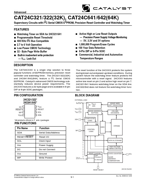
© 1998 by Catalyst Semiconductor, Inc. Characteristics subject to change without noticeDoc. No. 25083-00 12/989-1CAT24C321/322/641/6422AdvancedDoc. No. 25083-00 12/98ABSOLUTE MAXIMUM RATINGS*Temperature Under Bias....................–55°C to +125°C Storage Temperature........................ –65°C to +150°C Voltage on Any Pin withRespect to Ground (1) ..............–2.0V to +V CC + 2.0V V CC with Respect to Ground..................–2.0V to +7.0V Package Power DissipationCapability (Ta = 25°C)1.0W.................................1.0W Lead Soldering Temperature (10 secs)...............300°C Output Short Circuit Current (2) ..........................100mACOMMENTStresses above those listed under “Absolute Maximum Ratings” may cause permanent damage to the device.These are stress ratings only, and functional operation of the device at these or any other conditions outside of those listed in the operational sections of this specifica-tion is not implied. Exposure to any absolute maximum rating for extended periods may affect device perfor-mance and reliability.RELIABILITY CHARACTERISTICSSymbol Parameter Min.Max. Units Reference Test MethodN END (3)Endurance 1,000,000 Cycles/Byte MIL-STD-883, Test Method 1033 T DR (3)Data Retention 100 Years MIL-STD-883, Test Method 1008 V ZAP (3)ESD Susceptibility 2000 Volts MIL-STD-883, Test Method 3015 I LTH (3)(4)Latch-up 100 mAJEDEC Standard 17D.C. OPERATING CHARACTERISTICSV CC = +2.7V to +6.0V, unless otherwise specified.Symbol Parameter Min. Typ. Max. Units Test Conditions I CC Power Supply Current 3mA f SCL = 100 KHzIsbStandby Current40 µAVcc=3.3V50 µA Vcc=5I LI Input Leakage Current 2 µA V IN =G ND or V CC I LO Output Leakage Current10µA V IN =G ND or V CCV IL Input Low Voltage –1 V CC x 0.3 V V IH Input High Voltage V CC x 0.7 V CC + 0.5 VV OLOutput Low Voltage (SDA)0.4 V I OL = 3 mA ,V CC =3.0VLimitsCAPACITANCE T A = 25°C, f = 1.0 MHz, V CC = 5V Symbol Test Max.Units Conditions C I/O (3) Input/Output Capacitance (SDA)8pF V I/O = 0V C IN (3)Input Capacitance (SCL)6pFV IN = 0VNote:(1)The minimum DC input voltage is –0.5V. During transitions, inputs may undershoot to –2.0V for periods of less than 20 ns. Maximum DCvoltage on output pins is V CC +0.5V, which may overshoot to V CC + 2.0V for periods of less than 20ns.(2)Output shorted for no more than one second. No more than one output shorted at a time.(3)This parameter is tested initially and after a design or process change that affects the parameter.(4)Latch-up protection is provided for stresses up to 100 mA on address and data pins from –1V to V CC +1V.CAT24C321/322/641/6423AdvancedDoc. No. 25083-00 12/98A.C. CHARACTERISTICSV CC =2.7V to 6.0V unless otherwise specified.Output Load is 1 TTL Gate and 100pFRead & Write Cycle Limits SymbolParameterV CC =2.7V - 6V V CC =4.5V - 5.5V Min.Max.Min.Max.Units F SCL Clock Frequency100400kHz T I (1)Noise Suppression Time200200ns Constant at SCL, SDA Inputs t AA SCL Low to SDA Data Out 3.51µs and ACK Outt BUF (1)Time the Bus Must be Free Before 4.7 1.2µs a New Transmission Can Start t HD:STA Start Condition Hold Time 40.6µs t LOW Clock Low Period 4.7 1.2µs t HIGH Clock High Period40.6µs t SU:STA Start Condition Setup Time4.70.6µs (for a Repeated Start Condition)t HD:DAT Data In Hold Time 00ns t SU:DAT Data In Setup Time 5050ns t R (1)SDA and SCL Rise Time 10.3µs t F (1)SDA and SCL Fall Time 300300ns t SU:STO Stop Condition Setup Time 40.6µs t DHData Out Hold Time100100nsPower-Up Timing (1)(2)Symbol ParameterMax.Units t PUR Power-up to Read Operation 1ms t PUWPower-up to Write Operation1msNote:(1)This parameter is tested initially and after a design or process change that affects the parameter.(2)t PUR and t PUW are the delays required from the time V CC is stable until the specified operation can be initiated.Write Cycle Limits Symbol Parameter Min.Typ.Max Units t WRWrite Cycle Time10msThe write cycle time is the time from a valid stop condition of a write sequence to the end of the internal program/erase cycle. During the write cycle, the bus interface circuits are disabled, SDA is allowed to remain high, and the device does not respond to its slave address.CAT24C321/322/641/6424AdvancedDoc. No. 25083-00 12/98RESET CIRCUIT CHARACTERISTICSCAT24C321/322/641/6425AdvancedDoc. No. 25083-00 12/98PIN DESCRIPTIONSWP : WRITE PROTECTIf the pin is tied to V CC the entire memory array becomes Write Protected (READ only). When the pin is tied to V SS or left floating normal read/write operations are allowed to the device.SCL : SERIAL CLOCKThe serial clock input clocks all data transferred into or out of the device.RESET/RESET : RESET I/OThese are open drain pins and can be used as reset trigger inputs. By forcing a reset condition on the pins the device will initiate and maintain a reset condition for approximately 200ms. RESET pin must be connected through a pull-down and RESET pin must be connected through a pull-up device.SDA: SERIAL DATA/ADDRESSThe bidirectional serial data/address pin is used to transfer all data into and out of the device. The SDA pin is an open drain output and can be wire-ORed with other open drain or open collector outputs. In the 24C321/641, the SDA line is also used as the Watchdog Timer Monitor.Reset Controller DescriptionThe CAT24CXXX provides a precision RESET control-ler that ensures correct system operation during brown-out and power-up/down conditions. It is configured with open drain RESET outputs. During power-up, the RESET outputs remain active until V CC reaches the V TH threshold and will continue driving the outputs for approximately 200ms (t PURST ) after reaching V TH. After the t PURST timeout interval, the device will cease to drive reset outputs. At this point the reset outputs will be pulled up or down by their respective pull up/pull down devices. During power-down, the RESET outputs will begin driving active when V CC falls below V TH. The RESET outputs will be valid so long as V CC is >1.0V (V RVALID ).The RESET pins are I/Os; therefore, the CAT24CXXX can act as a signal conditioning circuit for an externally applied reset. The inputs are level triggered; that is, the RESET input in the 24CXXX will initiate a reset timeout after detecting a high and the RESET input in the 24CXXX will initiate a reset timeout after detecting a low.Watchdog TimerThe Watchdog Timer provides an independent protec-tion for microcontrollers. During a system failure, the CAT24C321/641 will respond with a reset signal after a time-out interval of 1.6 seconds for lack of activity.24CXX1 is designed with the Watchdog Timer feature on the SDA input. For the 24C321/641, if the microcontroller does not toggle the SDA input pin within 1.6 seconds the Watchdog Timer times out. This will generate a reset condition on reset outputs. The Watch-dog Timer is cleared by any transition on SDA.As long as the reset signal is asserted, the Watchdog Timer will not count and will stay cleared. 24C322/642does not feature the Watchdog Timer function.DEVICE OPERATIONV CCV RESETCAT24C321/322/641/6426AdvancedDoc. No. 25083-00 12/98Hardware Data ProtectionThe 24CXXX is designed with the following hardware data protection features to provide a high degree of data integrity.(1) The 24CXXX features a WP pin. When WP pin is tied high the entire memory array becomes write protected (read only).(2) The V CC sense provides write protection when V CC falls below the reset threshold value (V TH ). The V CC lock out inhibits writes to the serial EEPROM whenever V CC falls below (power down) V TH or until V CC reaches the reset threshold (power up) V TH .Reset Threshold VoltageFrom the factory the 24CXXX is offered in five different variations of reset threshold voltages. They are 4.50-4.75V, 4.25-4.50V, 3.00-3.15V, 2.85-3.00V and 2.55-2.70V. To provide added flexibility to design engineers using this product, the 24CXXX is designed with an additional feature of programming the reset threshold voltage. This allows the user to change the existing reset threshold voltage to one of the other four reset threshold voltages. Once the reset threshold voltage is selected it will not change even after cycling the power,unless the user uses the programmer to change the reset threshold voltage. However, the programming function is available only through third party programmer manufacturers. Please call Catalyst for a list of program-mer manufacturers who support this function.STOPCONDITIONSTARTCONDITIONADDRESSSCLSDAFigure 3. Write Cycle TimingSTART BITSDASTOP BITSCLFigure 4. Start/Stop TimingSCLSDA INSDA OUTFigure 2. Bus TimingCAT24C321/322/641/6427AdvancedDoc. No. 25083-00 12/98ACKNOWLEDGESTARTSCL FROM MASTERDATA OUTPUTFROM TRANSMITTERDATA OUTPUT FROM RECEIVERFigure 5. Acknowledge TimingFigure 6. Slave Address BitsFUNCTIONAL DESCRIPTIONThe CAT24CXXX supports the I 2C Bus data transmis-sion protocol. This Inter-Integrated Circuit Bus protocol defines any device that sends data to the bus to be a transmitter and any device receiving data to be a re-ceiver. The transfer is controlled by the Master device which generates the serial clock and all START and STOP conditions for bus access. The CAT24CXXX operates as a Slave device. Both the Master device and Slave device can operate as either transmitter or re-ceiver, but the Master device controls which mode is activated.I 2C BUS PROTOCOLThe features of the I 2C bus protocol are defined as follows:(1) Data transfer may be initiated only when the bus is not busy.(2) During a data transfer, the data line must remain stable whenever the clock line is high. Any changes in the data line while the clock line is high will be interpreted as a START or STOP condition.START ConditionThe START Condition precedes all commands to the device, and is defined as a HIGH to LOW transition of SDA when SCL is HIGH. The CAT24CXXX monitors the SDA and SCL lines and will not respond until this condition is met.STOP ConditionA LOW to HIGH transition of SDA when SCL is HIGH determines the STOP condition. All operations must end with a STOP condition.DEVICE ADDRESSINGThe Master begins a transmission by sending a START condition. The Master sends the address of the particu-lar slave device it is requesting. The four most significant bits of the 8-bit slave address are fixed as 1010.The next three bits are don't care. The last bit of the slave address specifies whether a Read or Write operation is to be performed. When this bit is set to 1, a Read operation is selected, and when set to 0, a Write opera-tion is selected.After the Master sends a START condition and the slave address byte, the CAT24CXXX monitors the bus and responds with an acknowledge (on the SDA line) when its address matches the transmitted slave address. The CAT24CXXX then performs a Read or Write operation depending on the state of the R/W bit.1010X R/WX XCAT24C321/322/641/6428AdvancedDoc. No. 25083-00 12/98Figure 7. Byte Write TimingFigure 8. Page Write TimingACKNOWLEDGEAfter a successful data transfer, each receiving device is required to generate an acknowledge. The Acknowledg-ing device pulls down the SDA line during the ninth clock cycle, signaling that it received the 8 bits of data.The CAT24CXXX responds with an acknowledge after receiving a START condition and its slave address. If the device has been selected along with a write operation,it responds with an acknowledge after receiving each 8-bit byte.When the CAT24CXXX begins a READ mode it trans-mits 8 bits of data, releases the SDA line, and monitors the line for an acknowledge. Once it receives this ac-knowledge, the CAT24CXXX will continue to transmit data. If no acknowledge is sent by the Master, the device terminates data transmission and waits for a STOP condition.WRITE OPERATIONSByte WriteIn the Byte Write mode, the Master device sends the START condition and the slave address information (with the R/W bit set to zero) to the Slave device. After t he Slave generates an acknowledge, the Master sends a 8-bit address that is to be written into the address pointers of the CAT24CXXX. After receiving another acknowledge from the Slave, the Master device trans-mits the data to be written into the addressed memory location. The CAT24CXXX acknowledges once more and the Master generates the STOP condition. At this time, the device begins an internal programming cycle to nonvolatile memory. While the cycle is in progress, the device will not respond to any request from the Master device.Page WriteThe 24CXXX writes up to 32 bytes of data in a single write cycle, using the Page Write operation. The page write operation is initiated in the same manner as the byte write operation, however instead of terminating after the initial byte is transmitted, the Master is allowed to send up to 31 additional bytes. After each byte has been transmitted, CAT24CXXX will respond with an acknowledge, and internally increment the lower order address bits by one. The high order bits remain un-changed.If the Master transmits more than 32 bytes before sending the STOP condition, the address counter ‘wraps around’, and previously transmitted data will be overwrit-ten.When all 32 bytes are received, and the STOP condi tion has been sent by the Master, the internal program-ming cycle begins. At this point, all received data is written to the CAT24CXXX in a single write cycle.* = Don't care bit for 24C321/322X= Don't care bitA 15–A 8SLAVE ADDRESSSA C KAC KDATAA C KS T O P P BUS ACTIVITY:MASTERSDA LINES T A R T A 7–A 0BYTE ADDRESS A C K*X X XSLAVE C KC KC KBUS ACTIVITY:MASTERSDA LINES T A BYTE ADDRESS C KS T C K C KC KCAT24C321/322/641/6429AdvancedDoc. No. 25083-00 12/98Figure 9. Immediate Address Read TimingAcknowledge PollingDisabling of the inputs can be used to take advantage of the typical write cycle time. Once the stop condition is issued to indicate the end of the host’s write operation,CAT24CXXX initiates the internal write cycle. ACK poll-ing can be initiated immediately. This involves issuing the start condition followed by the slave address for a write operation. If CAT24CXXX is still busy with the write operation, no ACK will be returned. If CAT24CXXX has completed the write operation, an ACK will be returned and the host can then proceed with the next read or write operation.WRITE PROTECTIONThe Write Protection feature allows the user to protect against inadvertent programming of the memory array.If the WP pin is tied to V CC , the entire memory array is protected and becomes read only. The CAT24CXXX will accept both slave and byte addresses, but the memory location accessed is protected from program-ming by the device's failure to send an acknowledge after the first byte of data is received.READ OPERATIONSThe READ operation for the CAT24CXXX is initiated in the same manner as the write operation with one excep-tion, that R/W bit is set to one. Three different READ operations are possible: Immediate/Current Address READ, Selective/Random READ and Sequential READ.SCL SDA 8TH BIT STOPNO ACKDATA OUT89SLAVE ADDRESSSA C KBUS ACTIVITY:MASTERSDA LINES T A R T N O A C KDATAS T O P PCAT24C321/322/641/64210AdvancedDoc. No. 25083-00 12/98Figure 10. Selective Read TimingFigure 11. Sequential Read TimingImmediate/Current Address ReadThe CAT24CXXX’s address counter contains the ad-dress of the last byte accessed, incremented by one. In other words, if the last READ or WRITE access was to address N, the READ immediately following would ac-cess data from address N+1. If N=E (where E=4095 for 24C321/322 and E=8191 for 24C641/642), then the counter will ‘wrap around’ to address 0 and continue to clock out data. After the CAT24CXXX receives its slave address information (with the R/W bit set to one), it issues an acknowledge, then transmits the 8-bit byte requested. The master device does not send an ac-knowledge, but will generate a STOP condition.Selective/Random ReadSelective/Random READ operations allow the Master device to select at random any memory location for a READ operation. The Master device first performs a ‘dummy’ write operation by sending the START condi-tion, slave address and byte addresses of the location it wishes to read. After CAT24CXXX acknowledges, the Master device sends the START condition and the slave address again, this time with the R/W bit set to one.The CAT24CXXX then responds with its acknowledge and sends the 8-bit byte requested. The master deviceSequential ReadThe Sequential READ operation can be initiated by either the Immediate Address READ or Selective READ operations. After the CAT24CXXX sends the initial 8-bit byte requested, the Master will respond with an acknowledge which tells the device it requires more data. The CAT24CXXX will continue to output an 8-bit byte for each acknowledge sent by the Master. The operation will terminate when the Master fails to respond with an acknowledge, thus sending the STOP condition.The data being transmitted from CAT24CXXX is output-ted sequentially with data from address N followed by data from address N+1. The READ operation address counter increments all of the CAT24CXXX address bits so that the entire memory array can be read during one operation. If more than E (where E= 4095 for 24C321/322, E=511 and E=8191 for 24C641/642) bytes are read out, the counter will ‘wrap around’ and continue to clock out data bytes.does not send an acknowledge but will generate a STOP condition.BUS ACTIVITY:MASTERSDA LINEDATA n+xDATA nC KC KDATA n+1C KS T O O A C KDATA n+2C KSLAVE ADDRESS* = Don't care bit for 24C321/322X= Don't care bitA 15–A 8SLAVE ADDRESSSA C KA C KA C KBUS ACTIVITY:MASTERSDA LINES T A R T A 7–A 0BYTE ADDRESS SLAVEADDRESSSA C KN O A C KS T A R T DATAPS T O P X X X *CAT24C321/322/641/64211Advanced Doc. No. 25083-00 12/98Ordering InformationNote:(1) The device used in the above example is a CAT24C322JI-30TE13 (32K I 2C Memory, SOIC, Industrial Temperature, 3.0-3.15V ResetThreshold Voltage, Tape and Reel)CAT24C321/322/641/64212AdvancedDoc. No. 25083-00 12/98。
AT24C32使用方法总结
2011-04-2916:56:58 分类:LINUXAT24C32是2-WireSerialEEPROM,容量为32Kbits(4096*8)。
利用该芯片可以模拟I2C总线,如果采用IO口来进行模拟,可以采用二线制(SCL、SDA),也可以采用三线制(WP、SCL、SDA)。
在编写驱动程序时,要分为两个层次。
第一、针对IIC总线的驱动部分。
第二、针对AT24C32的驱动部分。
DynamicC里面的IO模拟IIC函数库采用的是二线制,针对的芯片是24C02。
如果要用,就需要进行相应的改进。
下面把使用该芯片时注意的地方总结如下:1、各个引脚的含义A0-A2:地址线,用来选择slave器件。
WP:WriteProtect写保护,高电平拒绝写入,低电平可以写入,即低电平有效。
SCL:SerialClock串行时钟,用来指示什么时候数据线上是有效数据。
SDA:SerialData串行数据,用于数据传送2、关于WP脚二线制没有WP,也就是把WP置为低电平,始终写有效。
这样的问题是,在上电或调电的时候,可能会发生异常情况,对EEPROM内数据有所改动。
所以,如果有重要的数据,还是要采用WP引脚比较安全。
对AT24C32来说,WP置高,则只有四分之一受保护,即0x0C00-0x0FFF。
也就是说保护区为1KBytes。
对于低地址的四分之三,则不保护。
所以,如果数据较多时,可以有选择地存储。
不重要的数据则放在低四分之三区域,重要的数据则放在高四分之一区域。
看ICDatasheet,一定要仔细。
初次写测试程序时,发现WP不起作用,常有效。
用万用表测试,确实是高电平。
经过仔细阅读WP引脚说明,发现只有高四分之一区域可以写保护。
改变地址后,测试成功。
整个驱动函数也就修改成功了。
WP:Thewriteprotectinput,whentiedtoGND,,allwriteoperationstotheupperquand rant(8Kbits),WPisinternallypulleddowntoGND.3、关于读写流程AT24C32的数据地址必须要先发高字节地址,再发低字节地址。
联想ThinkAgile CP系列云平台产品指南说明书
Lenovo ThinkAgile CP Series Cloud PlatformProduct Guide (withdrawn product)Lenovo ThinkAgile CP Series is an all-in-one, composable cloud with an integrated application marketplace and end-to-end automation, delivering a turn-key cloud experience in your own data center. ThinkAgile CP Series uses modular compute, storage, and networking components paired with the cloud virtualization software to create pools of IT resources, independently scaling and allocating capacity, and automatically configuring resources to fulfill application requirements.Due to its software-defined modular architecture, the ThinkAgile CP Series platform can be scaled easily by adding more compute and storage resources independently of each other as your needs grow. Suggested workloads for the ThinkAgile CP Series include web services, virtual desktop infrastructure (VDI), enterprise applications, OLTP and OLAP databases, data analytics, application development, cost-optimized virtualization, containers, and other back-office applications.The following figure shows the ThinkAgile CP Series hardware components.Figure 1. Lenovo ThinkAgile CP Series hardware componentsDid you know?Lenovo professional deployment services are included in ThinkAgile CP Series to get customers up and running quickly. Also included is the ThinkAgile Advantage lifecycle management with a single point of support for the entire ThinkAgile CP platform with the nodes, networking, and software components, for quicker problem determination and minimized downtime.Lenovo offers additional professional services that can be purchased for the ThinkAgile CP Series deployments, including hardware installation, software deployment, workload migration, cloud assessment and design, and ongoing managed services to help achieve optimal operations and performance. ThinkAgile CP is designed to minimize downtime with all of the components engineered to work together, and with tested, standardized and automated code updates.Click here to check for updatesFigure 2. ThinkAgile CP Interconnect port-side viewThe following figure shows the non-port-side view of the ThinkAgile CP Interconnect. Figure 3. ThinkAgile CP Interconnect non-port-side viewThe following figure shows the rear view of the ThinkAgile CP Compute Block.Figure 5. ThinkAgile CP Compute Block rear viewFigure 6. ThinkAgile CP Storage Block front viewThe following figure shows the rear view of the ThinkAgile CP Storage Block.Figure 7. ThinkAgile CP Storage Block rear viewThe following figure shows the port-side view of the RackSwitch G7052.Figure 8. RackSwitch G7052 port-side viewThe following figure shows the non-port-side view of the RackSwitch G7052.Figure 9. RackSwitch G7052 non-port-side viewThe following figure shows the port-side view of the NE0152T RackSwitch.Figure 10. NE0152T RackSwitch port-side viewThe following figure shows the non-port-side view of the NE0152T RackSwitch.Figure 11. NE0152T RackSwitch non-port-side viewSystem specificationsThe following table lists the system specifications of the ThinkAgile CP Series. Table 1. ThinkAgile CP Series system specificationsAttribute SpecificationCP4000CP6000Warranty and support Three-, four-, or five-year customer-replaceable unit and onsite limited hardware warranty with ThinkAgile Advantage Support and selectable service levels: 9x5 next business day (NBD) parts delivered (base warranty), 9x5 NBD onsite response (Foundation Service), 24x7 coverage with 4-hour onsite response or 24-hour committed repair (select areas), (Essential Service), or 2-hour onsite response or 6-hour committed repair (select areas) (Advanced Service). Also available are YourDrive YourData, Premier Support, and Enterprise Software Support.Software Guardian Edition Software for ThinkAgile CP.Figure 12. ThinkAgile CP network connectivity topologyNote: When only one Interconnect is deployed with the CP4000 model, all ports on the Compute Block and Storage Block are connected to the same Interconnect network device.The following table lists the ThinkAgile CP Interconnect model.Table 2. Interconnect for CP SeriesDescription Machine Type/ModelThinkAgile CP Interconnect (CP-I-10)7Y67CTO1WW ThinkAgile CP Interconnect Expansion (CP-I-10E)7Y67CTO2WWConfiguration notes:Table 5. Transceivers and cables for customer network uplinksDescription FeaturecodeMaximum quantityper Interconnect10 GbE SFP+ DAC cables1.5m Passive DAC SFP+ Cable A51N2 2m Passive DAC SFP+ Cable A51P2 3m Passive DAC SFP+ Cable A1PJ2 5m Passive DAC SFP+ Cable A1PK2 7m Passive DAC SFP+ Cable A3RH2 10 GbE SFP+ active optical cablesLenovo 3m SFP+ to SFP+ Active Optical Cable ATYY2 Lenovo 5m SFP+ to SFP+ Active Optical Cable ATYZ2 Lenovo 7m SFP+ to SFP+ Active Optical Cable ATZ02 Lenovo 15m SFP+ to SFP+ Active Optical Cable ATZ12 Lenovo 20m SFP+ to SFP+ Active Optical Cable ATZ22 40 GbE QSFP+ transceivers and optical cablesLenovo 40GBASE-SR4 QSFP+ Transceiver A1DR2 Lenovo 10m QSFP+ MPO-MPO OM3 MMF Cable AT2U2 Lenovo 30m QSFP+ MPO-MPO OM3 MMF Cable AT2V2 40 GbE QSFP+ active optical cablesLenovo 3m QSFP+ to QSFP+ Active Optical Cable ATZ32 Lenovo 5m QSFP+ to QSFP+ Active Optical Cable ATZ42 Lenovo 7m QSFP+ to QSFP+ Active Optical Cable ATZ52 Lenovo 15m QSFP+ to QSFP+ Active Optical Cable ATZ62 Lenovo 20m QSFP+ to QSFP+ Active Optical Cable ATZ72 40 GbE QSFP+ to 4x10 GbE SFP+ active optical breakout cablesLenovo 1m QSFP+ to 4xSFP+ Active Optical Cable ATZ82 Lenovo 3m QSFP+ to 4xSFP+ Active Optical Cable ATZ92 Lenovo 5m QSFP+ to 4xSFP+ Active Optical Cable ATZA2 40 GbE QSFP+ direct-attach copper cablesLenovo 1m Passive QSFP+ DAC Cable A1DP2 Lenovo 3m Passive QSFP+ DAC Cable A1DQ2 Lenovo 5m Passive QSFP+ DAC Cable A2X82 Lenovo 7m Passive QSFP+ DAC Cable A2X92 40 GbE QSFP+ to 4x 10 GbE SFP+ breakout cablesLenovo 1m Passive QSFP+ to SFP+ Breakout DAC Cable A1DL2 Lenovo 3m Passive QSFP+ to SFP+ Breakout DAC Cable A1DM2 Lenovo 5m Passive QSFP+ to SFP+ Breakout DAC Cable A1DN2Intel Xeon Silver 4214 12C 85W 2.2GHz Processor B4HR Intel Xeon Silver 4214Y 12/10/8C 85W 2.2GHz Processor B4NW Intel Xeon Silver 4215 8C 85W 2.5GHz Processor B4HQ Intel Xeon Silver 4216 16C 100W 2.1GHz Processor B4HP Intel Xeon Gold processorsIntel Xeon Gold 5215 10C 85W 2.5GHz Processor B4HN Intel Xeon Gold 5215M 10C 85W 2.5GHz Processor B4P1 Intel Xeon Gold 5215L 10C 85W 2.5GHz Processor B4P9 Intel Xeon Gold 5217 8C 115W 3.0GHz Processor B4HM Intel Xeon Gold 5218 16C 125W 2.3GHz Processor B4HL Intel Xeon Gold 5218B 16C 125W 2.3GHz Processor B6BS Intel Xeon Gold 5218T 16C 105W 2.1GHz Processor B4P3 Intel Xeon Gold 5220 18C 125W 2.2GHz Processor B4HK Intel Xeon Gold 5220S 18C 125W 2.7GHz Processor B6CW Intel Xeon Gold 5220T 18C 105W 1.9GHz Processor B6CQ Intel Xeon Gold 6222V 20C 115W 1.8GHz Processor B6CV Intel Xeon Gold 6226 12C 125W 2.7GHz Processor B6CL Intel Xeon Gold 6230 20C 125W 2.1GHz Processor B4HJ Intel Xeon Gold 6230N 20C 125W 2.3GHz Processor B5RY Intel Xeon Gold 6230T 20C 125W 2.1GHz Processor B6CP Intel Xeon Gold 6234 8C 130W 3.3GHz Processor B6CK Intel Xeon Gold 6238 22C 140W 2.1GHz Processor B6CJ Intel Xeon Gold 6238M 22C 140W 2.1GHz Processor B6CM Intel Xeon Gold 6238L 22C 140W 2.1GHz Processor B6CR Intel Xeon Gold 6238T 22C 125W 1.9GHz Processor B4P2 Intel Xeon Gold 6240 18C 150W 2.6GHz Processor B4HH Intel Xeon Gold 6240M 18C 150W 2.6GHz Processor B6CN Intel Xeon Gold 6240L 18C 150W 2.6GHz Processor B6CS Intel Xeon Gold 6240Y 18/14/8C 150W 2.6GHz Processor B4NV Intel Xeon Gold 6242 16C 150W 2.8GHz Processor B4HG Intel Xeon Gold 6244 8C 150W 3.6GHz Processor B4HF Intel Xeon Gold 6246 12C 165W 3.3GHz Processor B6PD Intel Xeon Gold 6248 20C 150W 2.5GHz Processor B4HE Intel Xeon Gold 6252 24C 150W 2.1GHz Processor B4HC Intel Xeon Gold 6252N 24C 150W 2.3GHz Processor B6CT Intel Xeon Gold 6254 18C 200W 3.1GHz Processor B4HD Intel Xeon Gold 6262V 24C 135W 1.9GHz Processor B6CU Intel Xeon Platinum processorsIntel Xeon Platinum 8253 16C 125W 2.2GHz Processor B5RZ Intel Xeon Platinum 8260 24C 165W 2.4GHz Processor B4HB Intel Xeon Platinum 8260M 24C 165W 2.4GHz Processor B4NZManagement switchThe management network switch is a 1 GbE RJ-45 switch that connects SMM management ports on the Compute Blocks and management ports on the Storage Blocks. The management switch also provides one management uplink to the first Interconnect. The management switch can be purchased from Lenovo or provided by the customer.The following table lists the management switches that are available from Lenovo.Table 13. Management switchesDescription Machine Type-ModelFeaturecode QuantityRackSwitch G7052 (Rear to Front) for ThinkAgile CP7159-HCS B2ZC1 ThinkSystem NE0152T RackSwitch (Rear to Front) for ThinkAgile CP7Y81CTO4WW BAEU1The following tables list cables that are available for selection for the management switch.Table 14. 1 GbE UTP cables for management links to Compute Blocks and Storage BlocksDescription FeaturecodeMaximum quantityper switchQuantity perCompute BlockQuantity perStorage Block0.75m Blue Cat5e Cable AVFT16121.0m Blue Cat5e Cable AVFU1612 1.25m Blue Cat5e Cable AVFV1612 1.5m Blue Cat5e Cable38021612 3m Blue Cat5e Cable38031612 10m Blue Cat5e Cable38041612 25m Blue Cat5e Cable38051612Table 15. 10 GbE SFP+ cables for management uplink to InterconnectDescription FeaturecodeQuantityper switch10 GbE SFP+ DAC cables1.5m Passive DAC SFP+ Cable A51N1 2m Passive DAC SFP+ Cable A51P1 3m Passive DAC SFP+ Cable A1PJ1 5m Passive DAC SFP+ Cable A1PK1 7m Passive DAC SFP+ Cable A3RH1 10 GbE SFP+ active optical cablesLenovo 3m SFP+ to SFP+ Active Optical Cable ATYY1 Lenovo 5m SFP+ to SFP+ Active Optical Cable ATYZ1 Lenovo 7m SFP+ to SFP+ Active Optical Cable ATZ01 Lenovo 15m SFP+ to SFP+ Active Optical Cable ATZ11 Lenovo 20m SFP+ to SFP+ Active Optical Cable ATZ21Power cablesPower cablesThe following table lists the power cable options that can be selected for the ThinkAgile CP Series components. Two power cables are required per each Compute Block, Storage Block, Interconnect, and NE0152T management switch. One power cable is required for the G7052 management switch.Table 16. Power cablesDescription Feature codeRack power cables1.0m, 10A/125-250V, C13 to IEC 320-C14 Rack Power Cable A4VP1.5m, 10A/100-250V, C13 to IEC 320-C14 Rack Power Cable62012.0m, 13A/125V-10A/250V, C13 to IEC 320-C14 Rack Power Cable6570 2.8m, 10A/100-250V, C13 to IEC 320-C14 Rack Power Cable6311 2.8m, 13A/125V-10A/250V, C13 to IEC 320-C14 Rack Power Cable6400 2.8m, 10A/100-250V, C13 to IEC 320-C20 Rack Power Cable6204 4.3m, 10A/100-250V, C13 to IEC 320-C14 Rack Power Cable6263 4.3m, 13A/125V-10A/250V, C13 to IEC 320-C14 Rack Power Cable6583 Line cordsAustralia/New Zealand 2.8m, 10A/250V, C13 to AS/NZS 3112 Line Cord6211 Australia/New Zealand 4.3m, 10A/250V, C13 to AS/NZS 3112 Line Cord6574 Denmark 2.8m, 10A/250V, C13 to DK2-5a Line Cord6213 Denmark 4.3m, 10A/250V, C13 to DK2-5a Line Cord6575 Europe 2.8m, 10A/250V, C13 to CEE7-VII Line Cord6212 Europe 4.3m, 10A/250V, C13 to CEE7-VII Line Cord6572 India 2.8m, 10A/250V, C13 to IS 6538 Line Cord6269 India 4.3m, 10A/250V, C13 to IS 6538 Line Cord6567 Israel 2.8m, 10A/250V, C13 to SI 32 Line Cord6218 Israel 4.3m, 10A/250V, C13 to SI 32 Line Cord6579 Italy 2.8m, 10A/250V, C13 to CEI 23-16 Line Cord6217 Italy 4.3m, 10A/250V, C13 to CEI 23-16 Line Cord6493 South Africa 2.8m, 10A/250V, C13 to SABS 164 Line Cord6214 South Africa 4.3m, 10A/250V, C13 to SABS 164 Line Cord6576 Switzerland 2.8m, 10A/250V, C13 to SEV 1011-S24507 Line Cord6216 Switzerland 4.3m, 10A/250V, C13 to SEV 1011-S24507 Line Cord6578 United Kingdom 2.8m, 10A/250V, C13 to BS 1363/A Line Cord6215 United Kingdom 4.3m, 10A/250V, C13 to BS 1363/A Line Cord6577 United States 2.8m, 10A/250V, C13 to NEMA 6-15P Line Cord A1RF United States 4.3m, 10A/250V, C13 to NEMA 6-15P Line Cord6373Rack cabinetsThe following table lists the rack cabinets that are offered by Lenovo that can be used with the ThinkAgile CP Series.Table 20. Rack cabinetsDescription Part number25U S2 Standard Rack (1000 mm deep; 2 sidewall compartments)93072RX 25U Static S2 Standard Rack (1000 mm deep; 2 sidewall compartments)93072PX 42U S2 Standard Rack (1000 mm deep; 6 sidewall compartments)93074RX 42U 1100mm Enterprise V2 Dynamic Rack (6 sidewall compartments)93634PX 42U 1100mm Enterprise V2 Dynamic Expansion Rack (6 sidewall compartments)93634EX 42U 1200mm Deep Dynamic Rack (6 sidewall compartments)93604PX 42U 1200mm Deep Static Rack (6 sidewall compartments)93614PX 42U Enterprise Rack (1105 mm deep; 4 sidewall compartments)93084PX 42U Enterprise Expansion Rack (1105 mm deep; 4 sidewall compartments)93084EXFor more information, see the list of Product Guides in the Rack Cabinets category:/servers/options/racks#rt=product-guidePower distribution unitsThe following table lists the power distribution units (PDUs) that are offered by Lenovo that can be used with the ThinkAgile CP Series.Table 21. Power distribution unitsDescription Part number0U Basic PDUs0U 36 C13/6 C19 24A/200-240V 1 Phase PDU with NEMA L6-30P line cord00YJ776 0U 36 C13/6 C19 32A/200-240V 1 Phase PDU with IEC60309 332P6 line cord00YJ777 0U 21 C13/12 C19 32A/200-240V/346-415V 3 Phase PDU with IEC60309 532P6 cord00YJ778 0U 21 C13/12 C19 48A/200-240V 3 Phase PDU with IEC60309 460P9 line cord00YJ779 Switched and Monitored PDUs0U 20 C13/4 C19 Switched and Monitored 24A/200-240V/1Ph PDU w/ NEMA L6-30P cord00YJ781 0U 20 C13/4 C19 Switched and Monitored 32A/200-240V/1Ph PDU w/ IEC60309 332P6 cord00YJ780 0U 18 C13/6 C19 Switched and Monitored 32A/200-240/346-415V/3Ph PDU w/ IEC60309 532P6 cord00YJ782 0U 12 C13/12 C19 Switched and Monitored 48A/200-240V/3Ph PDU w/ IEC60309 460P9 cord00YJ783 1U 9 C19/3 C13 Switched and Monitored DPI PDU (without line cord)46M4002 1U 9 C19/3 C13 Switched and Monitored 60A 3Ph PDU with IEC 309 3P+Gnd cord46M4003 1U 12 C13 Switched and Monitored DPI PDU (without line cord)46M4004 1U 12 C13 Switched and Monitored 60A 3 Phase PDU with IEC 309 3P+Gnd line cord46M4005 Ultra Density Enterprise PDUs (9x IEC 320 C13 + 3x IEC 320 C19 outlets)Ultra Density Enterprise C19/C13 PDU Module (without line cord)71762NXUltra Density Enterprise C19/C13 PDU 60A/208V/3ph with IEC 309 3P+Gnd line cord 71763NU C13 Enterprise PDUs (12x IEC 320 C13 outlets)DPI C13 Enterprise PDU+ (without line cord)39M2816DPI Single Phase C13 Enterprise PDU (without line cord)39Y8941C19 Enterprise PDUs (6x IEC 320 C19 outlets)DPI Single Phase C19 Enterprise PDU (without line cord)39Y8948DPI 60A 3 Phase C19 Enterprise PDU with IEC 309 3P+G (208 V) fixed line cord 39Y8923Front-end PDUs (3x IEC 320 C19 outlets)DPI 30amp/250V Front-end PDU with NEMA L6-30P line cord 39Y8939DPI 32amp/250V Front-end PDU with IEC 309 2P+Gnd line cord 39Y8934DPI 60amp/250V Front-end PDU with IEC 309 2P+Gnd line cord 39Y8940DPI 63amp/250V Front-end PDU with IEC 309 2P+Gnd line cord 39Y8935Universal PDUs (7x IEC 320 C13 outlets)DPI Universal 7 C13 PDU (with 2 m IEC 320-C19 to C20 rack power cord)00YE443Line cords for PDUs that ship without a line cord DPI 30a Line Cord (NEMA L6-30P)40K9614DPI 32a Line Cord (IEC 309 P+N+G)40K9612DPI 32a Line Cord (IEC 309 3P+N+G)40K9611DPI 60a Cord (IEC 309 2P+G)40K9615DPI 63a Cord (IEC 309 P+N+G)40K9613DPI Australian/NZ 3112 Line Cord (32A)40K9617DPI Korean 8305 Line Cord (30A)40K9618DescriptionPart number For more information, see the list of Product Guides in the Power Distribution Units category:/servers/options/pdu#rt=product-guideUninterruptible power supply unitsUninterruptible power supply unitsThe following table lists the uninterruptible power supply (UPS) units that are offered by Lenovo that can be used with the ThinkAgile CP Series.Table 22. Uninterruptible power supply unitsDescription Part numberRT1.5kVA 2U Rack or Tower UPS (200-240VAC) (8x IEC 320 C13 10A outlets)55941KX RT2.2kVA 2U Rack or Tower UPS (200-240VAC) (8x IEC 320 C13 10A, 1x C19 16A outlets)55942KX RT3kVA 2U Rack or Tower UPS (200-240VAC) (8x IEC 320 C13 10A, 1x C19 16A outlets)55943KX RT5kVA 3U Rack or Tower UPS (200-240VAC) (8x IEC 320 C13 10A, 2x C19 16A outlets)55945KX RT6kVA 3U Rack or Tower UPS (200-240VAC) (8x IEC 320 C13 10A, 2x C19 16A outlets)55946KX RT8kVA 6U Rack or Tower UPS (200-240VAC) (4x IEC 320-C19 16A outlets)55948KX RT11kVA 6U Rack or Tower UPS (200-240VAC) (4x IEC 320-C19 16A outlets)55949KX RT8kVA 6U 3:1 Phase Rack or Tower UPS (380-415VAC) (4x IEC 320-C19 16A outlets)55948PX RT11kVA 6U 3:1 Phase Rack or Tower UPS (380-415VAC) (4x IEC 320-C19 16A outlets)55949PXFor more information, see the list of Product Guides in the Uninterruptible Power Supply Units category: /servers/options/ups#rt=product-guideLenovo Financial ServicesLenovo Financial Services reinforces Lenovo’s commitment to deliver pioneering products and services that are recognized for their quality, excellence, and trustworthiness. Lenovo Financial Services offers financing solutions and services that complement your technology solution anywhere in the world.We are dedicated to delivering a positive finance experience for customers like you who want to maximize your purchase power by obtaining the technology you need today, protect against technology obsolescence, and preserve your capital for other uses.We work with businesses, non-profit organizations, governments and educational institutions to finance their entire technology solution. We focus on making it easy to do business with us. Our highly experienced team of finance professionals operates in a work culture that emphasizes the importance of providing outstanding customer service. Our systems, processes and flexible policies support our goal of providing customers with a positive experience.We finance your entire solution. Unlike others, we allow you to bundle everything you need from hardware and software to service contracts, installation costs, training fees, and sales tax. If you decide weeks or months later to add to your solution, we can consolidate everything into a single invoice.Our Premier Client services provide large accounts with special handling services to ensure these complex transactions are serviced properly. As a premier client, you have a dedicated finance specialist who manages your account through its life, from first invoice through asset return or purchase. This specialist develops an in-depth understanding of your invoice and payment requirements. For you, this dedication provides a high-quality, easy, and positive financing experience.For your region-specific offers please ask your Lenovo sales representative or your technology provider about the use of Lenovo Financial Services. For more information, see the following Lenovo website:Related publications and linksTrademarksLenovo and the Lenovo logo are trademarks or registered trademarks of Lenovo in the United States, other countries, or both. A current list of Lenovo trademarks is available on the Web athttps:///us/en/legal/copytrade/.The following terms are trademarks of Lenovo in the United States, other countries, or both:Lenovo®Lenovo ServicesRackSwitchThinkAgile®ThinkSystem®TruDDR4XClarity®The following terms are trademarks of other companies:Intel® and Xeon® are trademarks of Intel Corporation or its subsidiaries.Linux® is the trademark of Linus Torvalds in the U.S. and other countries.Microsoft® is a trademark of Microsoft Corporation in the United States, other countries, or both.Other company, product, or service names may be trademarks or service marks of others.Lenovo ThinkAgile CP Series Cloud Platform (withdrawn product)31。
All-in-One 0.72° Stepper Motor Built-in Controller

All-in-One 0.72° Stepper MotorBuilt-in Controller Type PKA SeriesThis all-in-one 0.72° stepper motor features a built-incontroller (stored data) type, microstepping driver andhigh performance motor integrated into one compactpackage.There is no wiring needed between the controller,driver and motor, providing easy motion control of thehigh performance 0.72° stepper motor.There are three control methods that can be selected,I/O, Modbus (RTU)/RS-485 or Factory Automation (FA)Network.The controller and driver are integrated onto the 0.72º highperformance stepper motor. Since there is a built-in controllerthere is no need for a pulse generator. The system is simplified andrequires less wiring.By combining the high performance motor with a built-inmicrostepping driver and stored data controller, superior noise andvibration reduction can be easily achieved.Comparison of Vibration Characteristics2.01.61.20.80.4Speed [r/min]VibrationComponentVoltageVp-p[V]All-in-One Simplifies Motion ControlAdvantages of the All-in-One High Performance 0.72° Stepper MotorBuilt-in Controller (Stored Data) TypeDriver and ControllerMotorA positioning function is built-in, ensuring that the traveling amount, speed and other operating data is retained in the motor. It is also equipped with a variety of other operation functions in addition to the positioning operation, such as continuous operation and a return-to-home operation. This contributes to a reduced load on the programmable controller and a simplified program.All-in-One 0.72º Stepper MotorReduces the Burden on the Master ControllerPositioning Operation●The motor's operating speed and traveling amount are set in the operating data and operations are performed in accordance with the selected operating data.Linked Operation◇If the operating data is set to "linked", continuous positioning with the following data number is possible with one START signal.If data No. 01 is selected and the START input, the data No. 01 operation is executed. After that, it is stopped for only the set dwell time ✽ and then the operations from data No. 02 to No. 03 are executed. Operating data with a different rotation direction can also be linked.✽ Dwell time is the wait time until the nextpositioning operation starts.If data No. 01 is selected and the START input, linked driving from data No. 01 to No. 03 is performed without the motor stopping.Sequential Operation◇If the operating data is set to "sequential positioning", positioning of the next data number is performed in sequence every time a SSTART signal is input.I/OProgrammable ControllerThe positioning module (pulse generator) function is built-in to the driver, allowing theoperation to use I/O by directly connecting to a switch box or PLC. Because apositioning module is not necessary on the PLC side, space is saved and the system is simplified.Modbus (RTU)/RS-485Programmable ControllerComputerorOperating data and parameters can be set and operation commands can be input using RS-485 communication. Up to 31 drivers can be connected to each serial communication module. Also, there is a function that enables the simultaneous start of multiple axes. The protocol supports Modbus (RTU), enabling connection with devices such as touch screen (HMI) and PCs.Factory Automation (FA) NetworkUse of a network converter (sold separately)✽2 enables support with CC-Link, MECHATROLINK or EtherCAT communication. Operating data and parameters can be set and operationcommands can be input using various communication methods.Network Converter NETC01-CC (Sold separately)NETC01-M2 (Sold separately)NETC01-M3 (Sold separately)NETC01-ECT (Sold separately)Programmable Controller 2 A network converter converts✽various network protocols to the RS-485 communication protocol used in Oriental Motor products.Speed Control Operation●The motor operates continuously while a FWD signal or RVS signal is input. Because it operates at the speed of the operating data set beforehand, multistep speed-change operation is possible by changing the data number.FWD inputRVS input M0∼M5 inputMotor operationON OFF ON OFF ON OFF+Direction −DirectionReturn-To-Home Operation●Equipped with a sequence for return-to-home operation thatreduces the burden of the host (master controller) and the hassle of combining programs or sequences. A separate sensor is required.Touch Screen or Computer③FA Network② RS-485① I/O ② Modbus (RTU)② Modbus (RTU)CC-LinkMECHATROLINK-MECHATROLINK-EtherCATSystem Configuration■Example of System Configuration●The system configuration shown above is an example. Other combinations are also available.●Product Line■ 1 ✽Not supplied.2 ✽This is required for driving I/O control.3 ✽Compatible software can be downloaded from the Oriental Motor website.4 For details, please contact the nearest Oriental Motor sales office.✽N etwork ConverterSpecifications ■Speed – Torque Characteristics■PKA544KDPKA566KD0(0)10(100)5(50)15(150)Pulse Speed [kHz]Resolution: 500(Resolution: 5000)Speed [r/min]Current: 0.75 A/Phase Step Angle: 0.72˚/stepExternal Load Inertia: JL=0 kg·m (0 oz-in )T o r q u e [N ·m ]12C u r r e n t [A ]510152025T o r q u e [o z -i n]0(0)5(50)2.5(25)7.5(75)Speed [r/min]Pulse Speed [kHz]Resolution: 500(Resolution: 5000)Current: 1.4 A/Phase Step Angle: 0.72˚/step External Load Inertia: JL=0 kg·m (0 oz-in )T o r q u e [N ·m ] 024C u r r en t [A ]08012016040T o r q u e [o z -i n ]NoteDepending on the driving conditions, a considerable amount of heat may be generated by the motor. Be sure to keep the motor case temperature at 75˚C (167˚F) max.●Control Circuit Specifications■No. of Positioning Data Sets 64Operation FunctionsPositioning operation, return-to-home operation, continuous operation, JOG operation, test operationControl Circuit RS-485 Communication Specification■ProtocolModbus protocol (Modbus RTU mode)Electrical CharacteristicsEIA-485 complianceTwisted-pair wire (TIA/EIA-568B CAT5e or greater recommended) is used up to a total extension length of 50 m (164 ft.).Sending and Receiving Method Half-duplex communication Baud Rate 9600 bps/19200 bps/38400 bps/57600 bps/115200 bps Physical Layer Start-stop synchronization method (data: 8-bit, stop bit: 1-bit/2-bit, parity: none/odd/even)Connection Type Up to 31 units can be connected to one programmable controller (master controller).General Specifications■1 This value is for full step under no load. (The value changes with the size of the load.)✽2 Radial Play: Displacement in shaft position in the radial direction, when a 5 N (1.12 lb.) load is applied in the vertical direction to the tip of the motor's✽shaft.3 Axial Play: Displacement in shaft position in the axial direction, when a 10 N (2.2 lb.) load is applied to the motor shaft in the axial direction.✽4 T. I. R. (Total Indicator Reading): The total dial gauge reading when the measurement section is rotated one revolution centered on the reference axis✽center.Permissible Overhung Load and Permissible Thrust Load■Dimensions■Unit mm (in.)Motor●Frame Size 60 mm (2.36 in.)Connection Cable (Included)●Connection and Operation■Names and Function of Parts●Axis Setting Switch (SW2)Signal Monitor DisplayBaud Rate Setting Switch (SW3)Power Supply & I/O SignalConnector (CN1)RS-485 Communication Connector (CN2, 3)Control Module Connector (CN4)Signal Monitor Display LED Indicator◇Function Switch (SW1)Settings for RS-485 Communication Protocol◇Axis Setting Switch (SW2)Baud Rate Setting Switch (SW3)RS-485 Baud Rate Setting◇Power Supply & I/O Signal Connector (CN1)Sets the function to be assigned according to the parameter setting. The initial values are shown above. For details, refer to the User's Manual.✽The following input signals can be assigned to input terminals IN0∼3.1: FWD 9: MS124: ALM-RST 37: R545: R1353: M52: RVS 10: MS225: P-PRESET 38: R646: R1460: +LS 3: HOME 11: MS327: HMI 39: R747: R1561: −LS 4: START 12: MS432: R040: R848: M062: HOMES 5: SSTART 13: MS533: R141: R949: M163: SLIT6: +JOG 16: FREE 34: R242: R1050: M27: −JOG17: AWO35: R343: R1151: M31: FWD_R 10: MS2_R 34: R243: R1152: M4_R 68: MOVE 2: RVS_R 11: MS3_R 35: R344: R1253: M5_R 70: HOME-P 3: HOME_R 12: MS4_R 36: R445: R1360: +LS_R 72: TIM 4: START_R 13: MS5_R 37: R546: R1461: −LS_R 73: AREA15: SSTART_R 16: FREE_R 38: R647: R1562: HOMES_R 74: AREA26: +JOG_R 17: AWO_R 39: R748: M0_R 63: SLIT_R 75: AREA37: −JOG_R 18: STOP_R 40: R849: M1_R 65: ALM 80: S-BSY8: MS0_R32: R041: R950: M2_R66: WNGConnection Diagram●Connection to Programmable Controller◇Example of Connection with Current Sink Output Circuit (NPN specification)●Example of Connection with Current Source Output Circuit (PNP specification)●NotesUse 24 VDC for the input signals.●U se 24 VDC 10 mA max. for the output signals. When the current value exceeds 10 mA, connect the external resistor R to keep the current 10 mA max. ●If noise generated by the power supply cable causes a problem with the specific wiring or layout, shield the cable or use ferrite cores.●Control Module CableThis is a cable that connects an OPX-2A or data setting software communication cable to the PKA Series.Product Line■Dimensions■unit mm (in.)Accessories (Sold separately)These accessories are necessary to change operating data such as parameter settings and data settings in the PKA Series.Data Setting Software Communication CableThis communication cable is required for connecting to the computer on which the data setting software is installed.Product Line■orControl ModulePerform operations such as setting the driver's internal parameters and setting or changing the data. It can also be used for operations such as speed and I/O monitoring and teaching.Product Line■Specifications■IndicationLEDCable Length5 m (16.4 ft.)Operating Ambient Temperature0∼40˚C (+32∼+104˚F) (non-freezing)<Enlarged view>Dimensions■Unit mm (in.)Control Module●Mass: 0.25 kg (0.55 lb.)B453Panel Cut-Out for ●Controller Module[Installation Plate Thickness 1∼3 mm (0.04∼0.12 in.)]3.6220920 +0.8+0.031680 +0.7( (2.677 +0.0280))RS-485 Communication CableThis is an RS-485 communication cable.Product Line■Dimensions■unit mm (in.)CC020-RS4ACC020-RS4BOperating Environment■Operating System (OS)●Microsoft Windows 2000 Professional Service Pack 4●Be sure to install Rollup 1 provided by Microsoft Corporation. Check whether Rollup 1 has been installed in "Add or Remove Programs".For the following operating systems, both the 32-bit (x86) edition and 64-bit (x64) edition are supported.Microsoft Windows XP Home Edition Service Pack 3●Microsoft Windows XP Professional Service Pack 2●Microsoft Windows XP Professional Service Pack 3●✽1Microsoft Windows Vista Home Basic Service Pack 2●Microsoft Windows Vista Home Premium Service Pack 2●Microsoft Windows Vista Business Service Pack 2●Microsoft Windows Vista Ultimate Service Pack 2●Microsoft Windows Vista Enterprise Service Pack 2●Microsoft Windows 7 Starter Service Pack 1●Microsoft Windows 7 Home Premium Service Pack 1●Microsoft Windows 7 Professional Service Pack 1●Microsoft Windows 7 Ultimate Service Pack 1●Microsoft Windows 7 Enterprise Service Pack 1● 1 32-bit (x86) version only✽CC020-RS4ACC020-RS4BConnection Example●PC●Recommended CPU ✽2Intel Core processor 2 GHz min.(Must be compatible with OS)DisplayVideo adapter and monitor with resolution of XGA (1024 × 768) min.Recommended Memory ✽232-bit version (x86): 1 GB min.64-bit version (x64): 2 GB min.Hard Disk ✽3Free disk space of 30 MB B Port USB 1.1 1 PortDisk DeviceCD-ROM Drive (Used for installation)2 The operating conditions of the OS must be satisfied.✽3 Microsoft .NET Framework 2.0 Service Pack 2 is required for ✽MEXE02. If it is notinstalled, it will be installed automatically. An additional max. of 500 MB of free space may be required.NotesThe required memory and hard disk space may vary depending on the system environment. ●Windows and Windows Vista are registered trademarks of the Microsoft Corporation in the ●United States and other countries.Data Setting Software■MEXE02The data setting software can be downloaded from the Oriental Motor website. For details, please go to the Oriental Motor website or contact the nearest Oriental Motor sales office.A network converter converts from the hostcommunication protocols to Oriental Motor's own RS-485 communication protocol. Use the network converter to control products supporting Oriental Motor's RS-485 compatible products in the host communication environment.Features■Reduced Wiring and Space Saving is Possible●Only the one included cable is needed for the wiring when connecting to an RS-485-compatible product.Setting Method for Various Parameters●A control module OPX-2A (sold separately) or data setting software MEXE02 is required for setting a network converter.A control module OPX-2A and data setting software MEXE02 can also be used to monitor the time it takes to communicate with each axis.Multi-axis Connection is Possible●RS-485-compatible products can be connected on multiple -Link-compatible: 12 axes max.●MECHATROLINK-●-compatible: 16 axes max.MECHATROLINK-●-compatible: 16 axes max.EtherCAT-compatible: 16 axes max.●Product Line■The following items are included in each product.Network converter, RS-485 communication cable, power supply connector, operatingmanual, CC-Link communication connector (NETC01-CC only)Related Products (Sold separately)Network ConverterNETC01-CCNETC01-M2NETC01-M3NETC01-ECTCopyright ©2013 ORIENTAL MOTOR U.S.A. CORP .Printed in USA 13S #419Specifications are subject to change without notice. This catalog was published in May, 2013.ORIENTAL MOTOR U.S.A. CORP .Western Sales andCustomer Service Center Tel: (310) 715-3301 Fax: (310) 225-2594Los AngelesTel: (310) 715-3301San JoseTel: (408) 392-9735Midwest Sales andCustomer Service Center Tel: (847) 871-5900 Fax: (847) 472-2623ChicagoTel: (847) 871-5900DallasTel: (214) 432-3386TorontoTel: (905) 502-5333Eastern Sales andCustomer Service Center Tel: (781) 848-2426 Fax: (781) 848-2617BostonTel: (781) 848-2426CharlotteTel: (704) 766-1335New YorkTel: (973) 359-1100Technical SupportTel: (800) 468-3982 / 8:30 A.M. to 5:00 P .M., P .S.T. (M–F)7:30 A.M. to 5:00 P .M., C.S.T. (M–F)E-mail:*****************************Obtain Specifications, Online Training and Purchase Products at:。
滚动轴承习题和的答案解析
滚动轴承一、选择题11-1.滚动轴承代号由前置代号、基本代号和后置代号组成,其中基本代号表示_______。
A.轴承的类型、结构和尺寸 B. 轴承组件C.轴承内部结构变化和轴承公差等级 D. 轴承游隙和配置11-2.滚动轴承的类型代号由________表示。
A.数字B.数字或字母C. 字母D. 数字加字母11-3.________只能承受径向载荷。
A.深沟球轴承 B. 调心球轴承C. 圆锥滚子轴承D. 圆柱滚子轴承11-4.________ 只能承受轴向载荷。
A.圆锥滚子轴承 B. 推力球轴承C. 滚针轴承D. 调心滚子轴承11-5.________ 不能用来同时承受径向载荷和轴向载荷。
A. 深沟球轴承B. 角接触球轴承C. 圆柱滚子轴承11-6.角接触轴承承受轴向载荷的能力,随接触角α的增大而________。
A.增大 B.减小C.不变D.不定11-7.有a)7230C和b)7230AC两种滚动轴承,在相等的径向载荷作用下,它们的派生轴向力Sa和Sb相比较,应是________。
A.Sa >Sb B.Sa = SbC.Sa <Sb D.大小不能确定11-8.若转轴在载荷作用下弯曲变形较大或轴承座孔不能保证良好的同轴度,宜选用类型代号为________的轴承。
A.1或2 B.3或7C.N或NU D.6或NA11-9.一根用来传递转矩的长轴,采用三个固定在水泥基础上支点支承,各支点应选用的轴承类型为________。
A. 深沟球轴承B. 调心球轴承C. 圆柱滚子轴承D. 调心滚子轴承11-10.跨距较大并承受较大径向载荷的起重机卷筒轴轴承应选用________ 。
A. 深沟球轴承C. 调心滚子轴承D. 圆柱滚子轴承11-11.________ 轴承通常应成对使用。
A.深沟球轴承 B. 圆锥滚子轴承C. 推力球轴承D. 圆柱滚子轴承11-12.在正常转动条件下工作,滚动轴承的主要失效形式为________。
FM24CXX产品基本介绍以及应用领域概述

FM24CXX产品基本介绍以及应用领域概述(共2页)首先,简单介绍一下什么是EEPROM:EEPROM(Electrically Erasable Programmable Read一Only Memory)即电子擦除式只读存储器,它是一种非挥发性存储器,与擦除式只读存储器(EPROM)类似,电源消失后,储存的数据依然存在,要消除储存在其中的内容,不是用紫外线照射方式,而是以电子信号直接消除即可。
正是由于EEPROM具有以上特点,该器件可广泛应用于对数据存储安全性及可靠性要求高的应用场合,如门禁考勤系统,测量和医疗仪表,非接触式智能卡,税控收款机,预付费电度表或复费率电度表、水表、煤气表以及家电遥控器等应用场合。
该类型存储器在可靠数据存储领域会获得越来越广泛的应用。
但是,EEPROM有固定的使用寿命,这是指某一位由1写为O或由O写为1的次数。
不同厂家的产品,相同厂家不同型号、系列的产品,它们的寿命也不尽相同,100万次为常见主流产品。
24CXX系列在EEPROM产品中的位置:最常见的EEPROM有2线制串行EEPROM,3线制串行EEPROM,也有并行EEPROM。
在2线制串行EEPROM中又有适应不同总线的产品系列,其中24CXX是适用用于IIC总线的两线制串行EEPROM。
I2C(Inter-Integrated Circuit)总线是一种由PHILIPS公司开发的两线式串行总线,用于连接微控制器及其外围设备。
I2C总线产生于在80年代,最初为音频和视频设备开发,如今的应用领域涉及几乎所有有小容量字节存储需求的电子产品方案。
譬如每年在深圳就有IIC器件全球峰会,可见IIC器件的大量应用是将来通用类电子产品方案设计的首选。
I2C总线最主要的优点是其简单性和有效性。
由于接口直接在组件之上,因此I2C总线占用的空间非常小,减少了电路板的空间和芯片管脚的数量,降低了互联成本。
总线的长度可高达25英尺,并且能够以10Kbps的最大传输速率支持40个组件。
FM24C32中文资料

FM24C32U – 32K-Bit Standard 2-Wire Bus Interface Serial EEPROMInterface24IICFM Fairchild Non-VolatileMemoryFM24C32U – 32K-Bit Standard 2-Wire Bus Interface Serial EEPROMFM24C32U – 32K-Bit Standard 2-Wire Bus Interface Serial EEPROMBackground Information (IIC Bus) Extended IIC specification is an extension of Standard IIC speci-fication to allow addressing of EEPROMs with more than 16Kbits of memory on an IIC bus. The difference between the two specifications is that Extended IIC specification defines two bytes of “Array Address” information while Standard IIC specification defines only one. All other aspects are identical between the two specifications. Using two bytes of Array Address and 3 address signals (A2, A1 and A0), it is now possible to address up to 4 Mbits (28 * 28 * 23 * 8 = 4 Mbits) of memory on an IIC bus.Note that due to format difference, it is not possible to have peripherals which follow Standard IIC specification (e.g. 16K bit EEPROM) and peripherals which follow Extended IIC specifica-tion (e.g. 32K bit EEPROM) on a common IIC bus.IIC bus allows synchronous bi-directional communication be-tween a TRANSMITTER and a RECEIVER using a Clock signal (SCL) and a Data signal (SDA). Additionally there are up to three Address signals (A2, A1 and A0) which collectively serve as “chip select signal” to a device (e.g. EEPROM) on the bus.All communication on the IIC bus must be started with a valid START condition (by a MASTER), followed by transmittal (by the MASTER) of byte(s) of information (Address/Data). For every byte of information received, the addressed RECEIVER provides a valid ACKNOWLEDGE pulse to further continue the communi-cation unless the RECEIVER intends to discontinue the commu-nication. Depending on the direction of transfer (Write or Read), the RECEIVER can be a SLAVE or the MASTER. A typical IIC communication concludes with a STOP condition (by the MAS-TER).Addressing an EEPROM memory location involves sending a command string with the following information:[DEVICE TYPE]—[DEVICE/PAGE BLOCK SELECTION]—[R/W BIT]—[ARRAY ADDRESS#1]—[ARRAY ADDRESS#0] Slave AddressSlave Address is an 8-bit information consisting of a Device type field (4bits), Device/Page block selection field (3bits) and Read/ Write bit (1bit).Slave Address Format Device TypeIIC bus is designed to support a variety of devices such as RAMs, EPROMs etc., along with EEPROMS. Hence to properly identify various devices on the IIC bus, a 4-bit “Device Type” identifier string is used. For EEPROMS, this 4-bit string is 1-0-1-0. Every IIC device on the bus internally compares this 4-bit string to its own “Device Type” string to ensure proper device selection. Device/Page Block SelectionWhen multiple devices of the same type (e.g. multiple EEPROMS) are present on the IIC bus, then the A2, A1 and A0 address information bits are used in device selection. Every IIC device on the bus internally compares this 3-bit string to its own physical configuration (A2, A1 and A0 pins) to ensure proper device selection. This comparison is in addition to the “D evice Type”comparison.In addition to selecting an EEPROM, these 3 bits are also used to select a “page block” within the selected EEPROM. Each page block is 512Kbit (64 K Bytes) in size. If an EEPROM contains more than one page bock then the selection of a page block within the EEPROM is by using A2, A1 and A0 bits.Read/Write BitLast bit of the Slave Address indicates if the intended access is Read or Write. If the bit is "1," then the access is Read, whereas if the bit is "0," then the access is Write.AcknowledgeAcknowledge is an active LOW pulse on the SDA line driven by an addressed receiver to the addressing transmitter to indicate receipt of 8-bits of data. The receiver provides an ACK pulse for every 8-bits of data received. This handshake mechanism is done as follows: After transmitting 8-bits of data, the transmitter re-leases the SDA line and waits for the ACK pulse. The addressed receiver, if present, drives the ACK pulse on the SDA line during the 9th clock and releases the SDA line back (to the transmitter). Refer Figure 3.Array Address#1This is an 8-bit information containing the most significant 8-bits of 16-bit memory array address of a location to be selected within a page block of the device.Array Address#0This is an 8-bit information containing the least significant 8-bits of 16-bit memory array address of a location to be selected within a page block of the device.Device Type Identifier Device/Page BlockSelection1010A2A1A0R/W(LSB)FM24C32U – 32K-Bit Standard 2-Wire Bus Interface Serial EEPROMPin DescriptionsSerial Clock (SCL)The SCL input is used to clock all data into and out of the device. Serial Data (SDA)SDA is a bi-directional pin used to transfer data into and out of the device. It is an open drain output and may be wire–ORed with any number of open drain or open collector outputs.Write Protect (WP)If tied to V CC, PROGRAM operations onto the upper half (upper 16Kbits) of the memory will not be executed. READ operations are possible. If tied to V SS, normal operation is enabled, READ/ WRITE over the entire memory is possible.This feature allows the user to assign the upper half of the memory as ROM which can be protected against accidental programming. When write is disabled, slave address and word address will be acknowledged but data will not be acknowledged.This pin has an internal pull-down circuit. However, on systems where write protection is not required it is recommended that this pin is tied to V SS.Device Selection Inputs A2, A1 and A0 (as appropriate)These inputs collectively serve as “chip select” signal to an EEPROM when multiple EEPROMs are present on the same IIC bus. Hence these inputs should be connected to V CC or V SS in a unique manner to allow proper selection of an EEPROM amongst multiple EEPROMs. During a typical addressing sequence, every EEPROM on the IIC bus compares the configuration of these inputs to the respective 3 bit “D evice/Page block selection”information (part of slave address) to determine a valid selection. For e.g. if the 3 bit “Device/Page block selection” is 1-0-1, then the EEPROM whose “Device Selection inputs” (A2, A1 and A0) are connected to V CC-V SS-V CC respectively, is selected.Device OperationThe FM24C32U supports a bi-directional bus oriented protocol.The protocol defines any device that sends data onto the bus asa transmitter and the receiving device as the receiver. The devicecontrolling the transfer is the master and the device that iscontrolled is the slave. The master will always initiate datatransfers and provide the clock for both transmit and receive operations. Therefore, the FM24C32U will be considered a slavein all applications.Clock and Data ConventionsData states on the SDA line can change only during SCL LOW.SDA state changes during SCL HIGH are reserved for indicatingstart and stop conditions. Refer Figure 1.Start ConditionAll commands are preceded by the start condition, which is aHIGH to LOW transition of SD A when SCL is HIGH. The FM24C32U continuously monitors the SDA and SCL lines for the start condi-tion and will not respond to any command until this condition hasbeen met. Refer Figure 2.Stop ConditionAll communications are terminated by a stop condition, which is aLOW to HIGH transition of SDA when SCL is HIGH. The stopcondition is also used by the FM24C32U to place the device in thestandby power mode. Refer Figure 2.FM24C32U Array AddressingDuring Read/Write operations, addressing the EEPROM memoryarray involves in providing 2 address bytes, “Word Address 1” and“Word Address 0." However on FM24C32U only the 4 leastsignificant bits (LSB) of “Word Address 1” byte are used indecoding the access location. The remaining 4 bits are not usedand are recommended to be set to “0”. All 8 bits of the “WordAddress 0” byte are used in decoding the access location.FM24C32U – 32K-Bit Standard 2-Wire Bus Interface Serial EEPROMFM24C32U – 32K-Bit Standard 2-Wire Bus Interface Serial EEPROMFM24C32U – 32K-Bit Standard 2-Wire Bus Interface Serial EEPROMFM24C32U – 32K-Bit Standard 2-Wire Bus Interface Serial EEPROM。
- 1、下载文档前请自行甄别文档内容的完整性,平台不提供额外的编辑、内容补充、找答案等附加服务。
- 2、"仅部分预览"的文档,不可在线预览部分如存在完整性等问题,可反馈申请退款(可完整预览的文档不适用该条件!)。
- 3、如文档侵犯您的权益,请联系客服反馈,我们会尽快为您处理(人工客服工作时间:9:00-18:30)。
F MDCo nf i de n t i al© 2012 Fremont Micro Devices Inc. DS24C32_64-A0--page1Two-Wire Serial EEPROM32K, 64K (8-bit wide)FEATURES❑Low voltage and low power operations:FT24C32A/64A: V CC = 1.8V to 5.5V❑ Maximum Standby current < 1µA (typically 0.02µA and 0.06µA @ 1.8V and 5.5V respectively). ❑ 32 bytes page write mode.❑ Partial page write operation allowed.❑ Internally organized: 4,096 × 8 (32K), 8,192 × 8 (64K). ❑ Standard 2-wire bi-directional serial interface. ❑ Schmitt trigger, filtered inputs for noise protection. ❑ Self-timed Write Cycle (5ms maximum).❑ 800 kHz (5V), 400 kHz (1.8V, 2.5V, 2.7V) Compatibility. ❑ Automatic erase before write operation.❑ Write protect pin for hardware data protection.❑ High reliability: typically 1, 000,000 cycles endurance. ❑ 100 years data retention.❑ Industrial temperature range (-40℃ to 85℃).❑Standard 8-lead DIP/SOP/ MSOP/TSSOP/DFN and 5-lead SOT23/TSOT23 Pb-free packages.DESCRIPTIONThe FT24C32A/64A series are 32,768/65,536 bits of serial Electrical Erasable and Programmable Read Only Memory, commonly known as EEPROM. They are organized as 4096/8192 words of 8 bits (one byte) each. The devices are fabricated with proprietary advanced CMOS process for low power and low voltage applications. These devices are available in standard 8-lead DIP, 8-lead SOP, 8-lead MSOP, 8-lead TSSOP, 8-lead DFN, 5-lead SOT23, and 5-lead TSOT23 packages. A standard 2-wire serial interface is used to address all read and write functions. Our extended V CC range (1.8V to 5.5V) devices enables wide spectrum of applications.PIN CONFIGURATIONPin Name Pin Function A2, A1, A0 Device Address Inputs SDA Serial Data Input / Open Drain Output SCL Serial Clock Input WP Write Protect NC No-ConnectF MDCo nf i de nt i a l© 2012 Fremont Micro Devices Inc. DS24C32_64-A0--page2All these packaging types come in Pb-free certified.VCC WP SCL SDAA2A1A0GND8L DIP 8L SOP8L TSSOP 8L MSOP 8L DFN5L SOT235L TSOT23ABSOLUTE MAXIMUM RATINGSIndustrial operating temperature: -40℃ to 85℃ Storage temperature:-50℃ to 125℃Input voltage on any pin relative to ground: -0.3V to V CC + 0.3V Maximum voltage: 8VESD Protection on all pins: >2000V* Stresses exceed those listed under “Absolute Maximum Rating” may cause permanent damage to the device. Functional operation of the device at conditions beyond those listed in the specification is not guaranteed. Prolonged exposure to extreme conditions may affect device reliability or functionality .F MDCo nf i de nt i a l© 2012 Fremont Micro Devices Inc. DS24C32_64-A0--page3PIN DESCRIPTIONS(A) SERIAL CLOCK (SCL)The rising edge of this SCL input is to latch data into the EEPROM device while the falling edge of this clock is to clock data out of the EEPROM device. (B) DEVICE / CHIP SELECT ADDRESSES (A2, A1, A0)These are the chip select input signals for the serial EEPROM devices. Typically, these signals are hardwired to either V IH or V IL . If left unconnected, they are internally recognized as V IL . (C) SERIAL DATA LINE (SDA)SDA data line is a bi-directional signal for the serial devices. It is an open drain output signal and can be wired-OR with other open-drain output devices. (D) WRITE PROTECT (WP)The FT24C32A/64A devices have a WP pin to protect the whole EEPROM array from programming. Programming operations are allowed if WP pin is left un-connected or input to V IL . Conversely all programming functions are disabled if WP pin is connected to V IH or V CC . Read operations is not affected by the WP pin’s input level.MEMORY ORGANIZATIONThe FT24C32A/64A devices have 128/256 pages respectively. Since each page has 32 bytes, random word addressing to FT24C32A/64A will require 12/13 bits data word addresses respectively.DEVICE OPERATION(A) SERIAL CLOCK AND DATA TRANSITIONSThe SDA pin is typically pulled to high by an external resistor. Data is allowed to change only when Serial clock SCL is at V IL . Any SDA signal transition may interpret as either a START or STOP condition as described below.(B) START CONDITIONWith SCL V IH , a SDA transition from high to low is interpreted as a START condition. All valid commands must begin with a START condition.(C) STOP CONDITIONWith SCL V IH , a SDA transition from low to high is interpreted as a STOP condition. All valid read or write commands end with a STOP condition. The device goes into the STANDBY mode if it is after a read command. A STOP condition after page or byte write command will trigger the chip into the STANDBY mode after the self-timed internal programming finish (see Figure 1).(D) ACKNOWLEDGEThe 2-wire protocol transmits address and data to and from the EEPROM in 8 bit words. The EEPROM acknowledges the data or address by outputting a "0" after receiving each word. The ACKNOWLEDGE signal occurs on the 9th serial clock after each word.F MDCo nf i de nt i a l© 2012 Fremont Micro Devices Inc. DS24C32_64-A0--page4(E) STANDBY MODEThe EEPROM goes into low power STANDBY mode after a fresh power up, after receiving a STOP bit in read mode, or after completing a self-time internal programming operation.Figure 1: Timing diagram for START and STOP conditionsFigure 2: Timing diagram for output ACKNOWLEDGEDEVICE ADDRESSINGThe 2-wire serial bus protocol mandates an 8 bits device address word after a START bit condition to invoke a valid read or write command. The first four most significant bits of the device address must be 1010, which is common to all serial EEPROM devices. The next three bits are device address bits. These three device address bits (5th , 6th and 7th ) are to match with the external chip select/address pin states. If a match is made, the EEPROM device outputs an ACKNOWLEDGE signal after the 8th read/write bit, otherwise the chip will go into STANDBY mode. However, matching may not be needed for some or all device address bits (5th , 6th and 7th ) as noted below. The last or 8th bit is a read/write command bit. If the 8th bit is at V IH then the chip goes into read mode. If a “0” is detected, the device enters programming mode.SCLSDASTART Condition STOP ConditionData Data Valid Transition SCLData inData out START Condition ACKF MDCo nf i de nt i a l© 2012 Fremont Micro Devices Inc. DS24C32_64-A0--page5WRITE OPERATIONS(A) BYTE WRITEA write operation requires two 8-bit data word address following the device address word and ACKNOWLEDGE signal. Upon receipt of this address, the EEPROM will respond with a “0” and then clock in the first 8-bit data word. Following receipt of the 8-bit data word, the EEPROM will again output a “0”. The addressing device, such as a microcontroller, must terminate the write sequence with a STOP condition. At this time the EEPROM enters into an internally-timed write cycle state. All inputs are disabled during this write cycle and the EEPROM will not respond until the writing is completed (figure 3). (B) PAGE WRITEThe 32K/64K EEPROM are capable of 32-byte page write.A page write is initiated the same way as a byte write, but the microcontroller does not send a STOP condition after the first data word is clocked in. The microcontroller can transmit up to 31 more data words after the EEPROM acknowledges receipt of the first data word. The EEPROM will respond with a “0” after each data word is received. The microcontroller must terminate the page write sequence with a STOP condition (see Figure 4).The lower five bits of the data word address are internally incremented following the receipt of each data word. The higher data word address bits are not incremented, retaining the memory page row location. If more than 32 data words are transmitted to the EEPROM, the data word address will “roll over” and the previous data will be overwritten. (C) ACKNOWLEDGE POLLINGACKNOWLEDGE polling may be used to poll the programming status during a self-timed internal programming. By issuing a valid read or write address command, the EEPROM will not acknowledge at the 9th clock cycle if the device is still in the self-timed programming mode. However, if the programming completes and the chip has returned to the STANDBY mode, the device will return a valid ACKNOWLEDGE signal at the 9th clock cycle.READ OPERATIONSThe read command is similar to the write command except the 8th read/write bit in address word is set to “1”. The three read operation modes are described as follows: (A) CURRENT ADDRESS READThe EEPROM internal address word counter maintains the last read or write address plus one if the power supply to the device has not been cut off. To initiate a current address read operation, the micro-controller issues a START bit and a valid device address word with the read/write bit (8th ) set to “1”. The EEPROM will response with an ACKNOWLEDGE signal on the 9th serial clock cycle. An 8-bit data word will then be serially clocked out. The internal address word counter will then automatically increase by one. For current address read the micro-controller will not issue an ACKNOWLEDGE signal on the 18th clock cycle. The micro-controller issues a valid STOP bit after the 18th clock cycle to terminate the read operation. The device then returns to STANDBY mode (see Figure 5).(B) SEQUENTIAL READThe sequential read is very similar to current address read. The micro-controller issues a START bit and a valid device address word with read/write bit (8th ) set to “1”. The EEPROM will response with an ACKNOWLEDGE signal on the 9th serial clock cycle. An 8-bit data word will then be serially clocked out. Meanwhile the internally address word counter will then automatically increase by one.MDf i de nt i a l© 2012 Fremont Micro Devices Inc. DS24C32_64-A0--page6Unlike current address read, the micro-controller sends an ACKNOWLEDGE signal on the 18th clock cycle signaling the EEPROM device that it wants another byte of data. Upon receiving the ACKNOWLEDGE signal, the EEPROM will serially clocked out an 8-bit data word based on the incremented internal address counter. If the micro-controller needs another data, it sends out an ACKNOWLEDGE signal on the 27th clock cycle. Another 8-bit data word will then be serially clocked out. This sequential read continues as long as the micro-controller sends an ACKNOWLEDGE signal after receiving a new data word. When the internal address counter reaches its maximum valid address, it rolls over to the beginning of the memory array address. Similar to current address read, the micro-controller can terminate the sequential read by not acknowledging the last data word received, but sending a STOP bit afterwards instead (figure 6). (C) RANDOM READRandom read is a two-steps process. The first step is to initialize the internal address counter with a target read address using a “dummy write” instruction. The second step is a current address read.To initialize the internal address counter with a target read address, the micro-controller issues a START bit first, follows by a valid device address with the read/write bit (8th ) set to “0”. The EEPROM will then acknowledge. The micro-controller will then send two address words. Again the EEPROM will acknowledge. Instead of sending a valid written data to the EEPROM, the micro-controller performs a current address read instruction to read the data. Note that once a START bit is issued, the EEPROM will reset the internal programming process and continue to execute the new instruction - which is to read the current address (figure 7).Figure 3: Byte WriteSDA LINES T A R S BDEVICE S B /W C KW R I T FIRST WORD S BC KC KC KS B SECOND WORD S T O DATAFigure 4: Page WriteSDA LINES T A R S BDEVICE S B /W C KW R I T FIRST WORD S BC KC KC KS B SECOND WORD S T OC KFDCo ne nt i a l© 2012 Fremont Micro Devices Inc. DS24C32_64-A0--page7Figure 5: Current Address ReadSDA LINES T A R S BDEVICE S B /W C KR E A DO A C KS T O DATAFigure 6: Sequential ReadDEVICE /W R E A DC KO A C KS T O DATA (N)DATA (N+1)DATA (N+2)DATA (N+3)C KC KC KFigure 7: Random ReadS T A R S BDEVICE S B /W C R E A DKO A C KS T O DATA (N)S T A R S BDEVICE S B /W C KW R I T FIRST WORD S BC KS B SECOND WORD C KSDA LINENotes: 1) * = Don’t Care bits2) # = Don’t Care bits for FT24C32F MDCo nf i de nt i© 2012 Fremont Micro Devices Inc. DS24C32_64-A0--page8Figure 8: SCL and SDA Bus TimingSCLSDA INSDA OUTAC CHARACTERISTICS1.8V2.5-5.0 VSymbolParameter Min Max Min Max Unitf SCL Clock frequency, SCL400800 kHz t LOW Clock pulse width low 1.20.9µst HIGH Clock pulse width high0.4 0.3 µs t I Noise suppression time (1)180 120 nst AA Clock low to data out valid0.3 1.2 0.2 0.9 µs t BUF Time the bus must be free before a newtransmission can start (1) 1.3 1.2 µst HD.STA START hold time0.6 0.6 µs t SU.STA START set-up time0.6 0.6 µs t HD.DAT Data in hold time 0 0 µs t SU.DAT Data in set-up time 100100nst R Input rise time (1) 0.3 0.3 µst F Input fall time (1)300 300 nst SU.STO STOP set-up time 0.6 0.6 µs t DH Date out hold time 200 50 ns t WRWrite cycle time55msEndurance (1) 25o C, Page Mode, 3.3V1,000,000Write CyclesNotes: 1. This Parameter is expected by characterization but are not fully screened by test.2. AC Measurement conditions: R L (Connects to Vcc): 1.3K ΩInput Pulse Voltages: 0.3Vcc to 0.7VccInput and output timing reference Voltages: 0.5VccF MDe nt i a l© 2012 Fremont Micro Devices Inc. DS24C32_64-A0--page9DC CHARACTERISTICSSymbol Parameter Test ConditionsMin Typical Max Units V CC1 24C ××A supply V CC1.8 5.5 V I CC Supply read current V CC @ 5.0V SCL = 400 kHz 0.4 1.0 mA I CCSupply write currentV CC @ 5.0V SCL = 400 kHz2.03.0mAI SB1 Supply current V CC @ 1.8V, V IN = V CC or V SS 0.02 1.0 µA I SB2 Supply current V CC @ 2.5V, V IN = V CC or V SS 1.0 µA I SB3 Supply current V CC @ 5.0V, V IN = V CC or V SS 0.07 1.0 µAI IL Input leakage current V IN = V CC or V SS 3.0 µA I LO Output leakage current V IN = V CC or V SS3.0µA V IL Input low level -0.6V CC × 0.3V V IH Input high levelV CC × 0.7V CC + 0.5VV OL2 Output low level V CC @ 3.0V, I OL = 2.1 mA0.4 VV OL1 Output low levelV CC @ 1.8V, I OL = 0.15 mA0.2 VORDERING INFORMATIONDensity PackageTemperature RangeVcc HSF Packaging Ordering CodeRoHSTube FT24C32A-UDR-BDIP8 -40℃-85℃ 1.8V-5.5VGreenTube FT24C32A-UDG-B Tube FT24C32A-USR-B RoHSTape and Reel FT24C32A-USR-TTube FT24C32A-USG-B SOP8 -40℃-85℃ 1.8V-5.5VGreen Tape and Reel FT24C32A-USG-TTube FT24C32A-UMR-B RoHSTape and Reel FT24C32A-UMR-TTube FT24C32A-UMG-B 32kbitsMSOP8 -40℃-85℃ 1.8V-5.5VGreenTape and Reel FT24C32A-UMG-TD: DIP8 S: SOP8 M: MSOP8 T: TSSOP8 L: SOT23-5 P: TSOT23-5 N: DFN8PackagingB: TubeT: Tape and Reel HSF R: RoHS G: GreenU:-40F MDCo nf i de nt i a l© 2012 Fremont Micro Devices Inc. DS24C32_64-A0--page10Tube FT24C32A-UTR-B RoHSTape and Reel FT24C32A-UTR-TTube FT24C32A-UTG-B TSSOP8 -40℃-85℃ 1.8V-5.5VGreenTape and Reel FT24C32A-UTG-T RoHS Tape and Reel FT24C32A-ULR-T SOT23-5-40℃-85℃1.8V-5.5VGreen Tape and Reel FT24C32A-ULG-T RoHSTape and Reel FT24C32A-UPR-T TSOT23-5 -40℃-85℃ 1.8V-5.5VGreen Tape and Reel FT24C32A-UPG-T RoHSTape and Reel FT24C32A-UNR-T 32kbitsDFN8 -40℃-85℃ 1.8V-5.5VGreen Tape and Reel FT24C32A-UNG-TRoHSTube FT24C64A-UDR-B DIP8 -40℃-85℃ 1.8V-5.5VGreen Tube FT24C64A-UDG-B Tube FT24C64A-USR-B RoHSTape and Reel FT24C64A-USR-TTube FT24C64A-USG-B SOP8 -40℃-85℃ 1.8V-5.5VGreen Tape and Reel FT24C64A-USG-TTube FT24C64A-UMR-B RoHSTape and Reel FT24C64A-UMR-TTube FT24C64A-UMG-B MSOP8 -40℃-85℃ 1.8V-5.5VGreenTape and Reel FT24C64A-UMG-TTube FT24C64A-UTR-B RoHSTape and Reel FT24C64A-UTR-TTube FT24C64A-UTG-B TSSOP8 -40℃-85℃ 1.8V-5.5VGreen Tape and Reel FT24C64A-UTG-T RoHSTape and Reel FT24C64A-ULR-T SOT23-5 -40℃-85℃ 1.8V-5.5VGreen Tape and Reel FT24C64A-ULG-T RoHSTape and Reel FT24C64A-UPR-T TSOT23-5 -40℃-85℃ 1.8V-5.5VGreen Tape and Reel FT24C64A-UPG-T RoHSTape and Reel FT24C64A-UNR-T 64kbitsDFN8 -40℃-85℃ 1.8V-5.5VGreenTape and Reel FT24C64A-UNG-TF MDCo nf i de nt i al© 2012 Fremont Micro Devices Inc. DS24C32_64-A0--page11DIP8 PACKAGE OUTLINEDIMENSIONSDimensions In MillimetersDimensions In InchesSymbolMin Max Min MaxA 3.710 4.310 0.146 0.170 A1 0.510 0.020 A2 3.200 3.600 0.126 0.142B 0.380 0.570 0.015 0.022B1 1.524(BSC ) 0.060(BSC ) C 0.204 0.360 0.008 0.014 D 9.000 9.400 0.354 0.370 E 6.200 6.600 0.244 0.260 E1 7.320 7.920 0.288 0.312 e 2.540 (BSC) 0.100(BSC ) L 3.000 3.600 0.118 0.142 E2 8.400 9.000 0.331 0.354F MDCo nf i de nt i al© 2012 Fremont Micro Devices Inc. DS24C32_64-A0--page12SOP8 PACKAGE OUTLINE DIMENSIONSDimensions In MillimetersDimensions In InchesSymbolMin Max Min MaxA 1.350 1.750 0.053 0.069A1 0.100 0.250 0.004 0.010A2 1.350 1.550 0.053 0.061 b 0.330 0.510 0.013 0.020 c 0.170 0.250 0.006 0.010D 4.700 5.100 0.185 0.200E 3.800 4.000 0.150 0.157 E1 5.800 6.200 0.228 0.244 e 1.270 (BSC)0.050 (BSC)L 0.400 1.270 0.016 0.050 θ 0° 8° 0° 8°F MDCo nf i de nt i a l© 2012 Fremont Micro Devices Inc. DS24C32_64-A0--page13MSOP8 PACKAGE OUTLINE DIMENSIONSDimensions In MillimetersDimensions In InchesSymbolMin Max Min MaxA 0.820 1.100 0.320 0.043 A1 0.020 0.150 0.001 0.006 A2 0.750 0.950 0.030 0.037 b 0.250 0.380 0.010 0.015 c 0.090 0.230 0.004 0.009 D 2.900 3.100 0.114 0.122 e 0.65 (BSC) 0.026 (BSC) E 2.900 3.100 0.114 0.122 E1 4.750 5.050 0.187 0.199 L 0.400 0.800 0.016 0.031 θ 0° 6° 0° 6°F MDC o n f i de nt i a l© 2012 Fremont Micro Devices Inc. DS24C32_64-A0--page14TSSOP8 PACKAGE OUTLINEDIMENSIONSDimensions In Millimeters Dimensions In InchesSymbolMinMax Min Max D 2.900 3.100 0.114 0.122 E4.3004.5000.1690.177b 0.190 0.300 0.007 0.012c 0.090 0.200 0.004 0.008 E1 6.250 6.550 0.246 0.258 A 1.100 0.043 A2 0.800 1.000 0.031 0.039 A1 0.020 0.150 0.001 0.006e 0.65 (BSC) 0.026 (BSC) L 0.500 0.700 0.020 0.028H 0.25 (TYP) 0.01 (TYP)θ 1°7° 1° 7°F MDCo nf i de n t i a l© 2012 Fremont Micro Devices Inc. DS24C32_64-A0--page15SOT-23-5 PACKAGE OUTLINE DIMENSIONSDimensions In MillimetersDimensions In InchesSymbolMin Max Min MaxA 1.050 1.250 0.041 0.049 A1 0.000 0.100 0.000 0.004 A2 1.050 1.150 0.041 0.045 b 0.300 0.500 0.012 0.020 c 0.100 0.200 0.004 0.008 D 2.820 3.020 0.111 0.119 E 1.500 1.700 0.059 0.067 E1 2.650 2.950 0.104 0.116 e 0.95 (BSC) 0.037 (BSC) e1 1.800 2.000 0.071 0.079 L 0.300 0.600 0.012 0.024 θ 0° 8° 0° 6°F MDCo nf i de nt i a l© 2012 Fremont Micro Devices Inc. DS24C32_64-A0--page16TSOT-23-5 PACKAGE OUTLINE DIMENSIONSDimensions In MillimetersDimensions In InchesSymbolMin Max Min MaxA 0.700 0.900 0.028 0.035 A1 0.000 0.100 0.000 0.004 A2 0.700 0.800 0.028 0.031 b 0.350 0.500 0.014 0.020 c 0.080 0.200 0.003 0.008 D 2.820 3.020 0.111 0.119 E 1.600 1.700 0.063 0.067 E1 2.650 2.950 0.104 0.116 e 0.95 (BSC) 0.037 (BSC) e1 1.90 (BSC) 0.075 (BSC) L 0.300 0.600 0.012 0.024 θ 0° 8° 0° 8°F MDCo nf i de nt i a l© 2012 Fremont Micro Devices Inc. DS24C32_64-A0--page17DFN8 PACKAGE OUTLINE DIMENSIONSDimensions In MillimetersSymbolMinNomMaxA 0.70 0.75 0.80 A1 - 0.02 0.05 b 0.18 0.25 0.03 c 0.18 0.20 0.25 D 1.902.00 2.10D2 1.50REF e 0.50BSC Nd 1.50BSC E 2.90 3.00 3.10 E2 1.60REFL 0.30 0.40 0.50 h 0.20 0.25 0.30* Information furnished is believed to be accurate and reliable. However, Fremont Micro Devices, Incorporated (BVI) assumes no responsibility for the consequences of use of such information or for any infringement of patents of other rights of third parties which may result from its use. No license is granted by implication or otherwise under any patent rights of Fremont Micro Devices, Incorporated (BVI). Specifications mentioned in this publication are subject to change without notice. This publication supersedes and replaces all information previously supplied. Fremont Micro Devices, Incorporated (BVI) products are not authorized for use as critical components in life support devices or systems without express written approval of Fremont Micro Devices, Incorporated (BVI). The FMD logo is a registered trademark of Fremont Micro Devices, Incorporated (BVI). All other names are the property of their respective owners.© 2012 Fremont Micro Devices Inc. DS24C32_64-A0--page18 DMF。