MAX4362中文资料
max9722中文资料

AAX
0.8mm)
MAX9722AEUE -40°C to +85°C 16 TSSOP
—
16 Thin QFN-EP*
MAX9722BETE -40°C to +85°C (3mm ✕ 3mm ✕
AAY
0.8mm)
MAX9722BEUE -40°C to +85°C 16 TSSOP
—
*EP = Exposed paddle.
________________________________________________________________ Maxim Integrated Products 1
本文是 Maxim正式英文资料的译文,Maxim不对翻译中存在的差异或由此产生的错误负责。请注意译文中可能存在文字组织或 翻译错误,如需确认任何词语的准确性,请参考 Maxim提供的英文版资料。 索取免费样品和最新版的数据资料,请访问 Maxim的主页:。
16-Pin Thin QFN (derate 14.7mW/°C above +70°C)....1176mW 16-Pin TSSOP (derate 9.4mW/°C above +70°C) .........755mW Junction Temperature ......................................................+150°C Operating Temperature Range............................-40°C to +85°C Storage Temperature Range .............................-65°C to +150°C Lead Temperature (soldering, 10s) .................................+300°C
MAX1232

④ 选择看门狗定时器时间必须充分考虑到程序设计中的中断嵌套、多重调用、查询等待、与外部低速器件(如液晶显示屏)接口等影响程序完成一个循环所需时间的各种因素并适当留有余量,否则容易产生意外的看门狗复位。具体时间应由试验决定。在设计初始阶段最稳妥的办法,是在监控芯片的时间选择端设置拨位开关,以便根据实际情况进行选择。
因此,从程序运行产生错误到DSP芯片完成复位,将有共计1.8 s的非受控时间,这对于对实时性要求很高的电力故障录波器来说是不能忍受的。如果在此期间电网发生故障,录波器将无法作出正确的反应。很显然,必须寻找一种具有适合看门狗定时器时间和复位脉冲宽度的硬件监控芯片。
在这里,必须明确对看门狗定时器时间的选择条件。在程序设计中,为了保证硬件监控效果,不宜过多地设置对看门狗芯片的操作,一般应在程序循环的关键部位设置1~2处对看门狗芯片的触发操作。所以,看门狗定时器的时间只要大于一个需时最长的程序循环即可。在基于F206的故障录波器中,需时最长的程序循环包含1个16点的FFT运算,整个程序循环的总时间小于2 ms。
由此看来,硬件监控电路的看门狗时间只要大于2 ms即可满足要求,过长的看门狗时间是不必要的,对保证装置的实时性也是十分不利的。
2 MAX6369~MAX6374监控芯片的原理及应用
根据以上标准,我们选用了MAXIM公司出品的MAX6374监控芯片。MAX6374是MAX6369~ MAX6374系列监控芯片中的一员。该系列芯片的看门狗定时器时间可以通过外部引脚SET2、SET1、SET0的逻辑电平进行精确调节,其引脚电平与看门狗定时器时间的关系如表1所列。
但是,根据我们的设计经验和对系统运行的仔细分析,使用MAX706等类似的许多硬件监控芯片存在2个需要注意的问题:第一,看门狗定时器的时间过长,MAX706的典型时间为1.6 s,也就是说,当DSP中的程序运行产生错误时,MAX706要在 1.6 s(相当于80个工频周期)后才能发出复位信号。第二,监控芯片输出的复位信号脉冲宽度过大,MAX706的典型值为200 ms(相当于10个工频周期),这主要是为了兼顾上电复位时对晶振100~300 ms稳定期的要求。
MAX485中文数据手册资料
MAX485中文资料2009-11-28 14:49MAX485中文资料,MAX485 PDF,DATASHEET,电路图,通讯程序内容介绍:MAX481、MAX483、MAX485、MAX487-MAX491以及MAX1487是用于RS-485与RS-422通信的低功耗收发器,每个器件中都具有一个驱动器和一个接收器。
MAX483、MAX487、MAX488以及MAX489具有限摆率驱动器,可以减小EMI,并降低由不恰当的终端匹配电缆引起的反射,实现最高250kbps 的无差错数据传输。
MAX481、MAX485、MAX490、MAX491、MAX1487的驱动器摆率不受限制,可以实现最高2.5Mbps的传输速率。
这些收发器在驱动器禁用的空载或满载状态下,吸取的电源电流在120(A 至500(A 之间。
另外,MAX481、MAX483与MAX487具有低电流关断模式,仅消耗0.1µA。
所有器件都工作在5V单电源下。
驱动器具有短路电流限制,并可以通过热关断电路将驱动器输出置为高阻状态,防止过度的功率损耗。
接收器输入具有失效保护特性,当输入开路时,可以确保逻辑高电平输出。
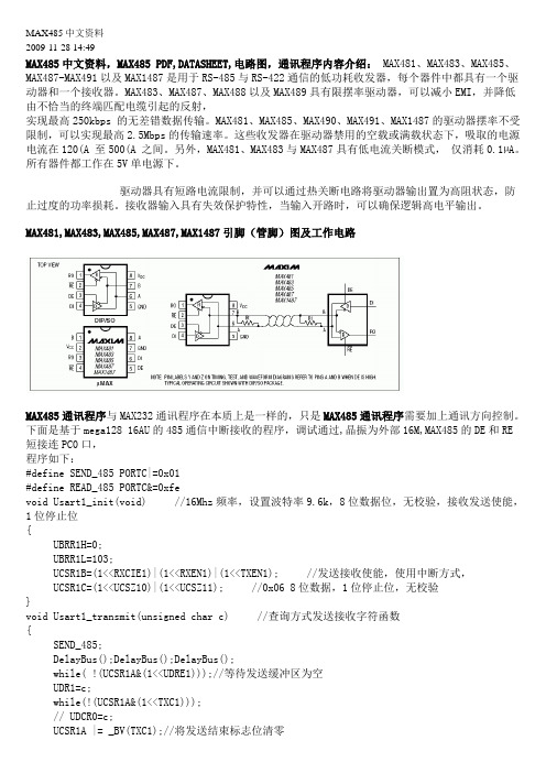
MAX481,MAX483,MAX485,MAX487,MAX1487引脚(管脚)图及工作电路MAX485通讯程序与MAX232通讯程序在本质上是一样的,只是MAX485通讯程序需要加上通讯方向控制。
下面是基于mega128 16AU的485通信中断接收的程序,调试通过,晶振为外部16M,MAX485的DE和RE短接连PC0口,程序如下:#define SEND_485 PORTC|=0x01#define READ_485 PORTC&=0xfevoid Usart1_init(void) //16Mhz频率,设置波特率9.6k,8位数据位,无校验,接收发送使能,1位停止位{UBRR1H=0;UBRR1L=103;UCSR1B=(1<<RXCIE1)|(1<<RXEN1)|(1<<TXEN1); //发送接收使能,使用中断方式,UCSR1C=(1<<UCSZ10)|(1<<UCSZ11); //0x06 8位数据,1位停止位,无校验}void Usart1_transmit(unsigned char c) //查询方式发送接收字符函数{SEND_485;DelayBus();DelayBus();DelayBus();while( !(UCSR1A&(1<<UDRE1)));//等待发送缓冲区为空UDR1=c;while(!(UCSR1A&(1<<TXC1)));// UDCR0=c;UCSR1A |= _BV(TXC1);//将发送结束标志位清零// SET_BIT(UCSR1A,);READ_485;direction++;}SIGNAL(SIG_UART1_RECV)//serial port 1 {if(UCSR1A&(1<<RXC1)){rec1buff=UDR1;rec1_flag=1;。
MAX232中文资料,MAX232CPE,MAX232EPE,MAX232ECPE,规格书,MAXIM代理商,datasheet,PDF
19-4323; Rev 15; 13;5V ޥ٫Ăۂ لRS-232 ഝڑಹ/ेฏಹ
________________________________ ݣะ
MAX220–MAX249࿅઼ഝڑಹ /ेฏಹLjከཛྷEIA/TIA232EჾࣆV.28/V.24ဳेਊහࣜLjᅐದกྐۨ໗ ޥ±12V ٫ᆚوᄮᅋă
ሦဗಹऔ໎Ӽคࠩ٫֠ޥ٫࿅༇Ljሦกᅑᅢದّڱߔࠞޢ ன৹ჾटࠞޢऋဏ ف5μW ჾăMAX225ĂMAX233Ă MAX235 ჾࣆ MAX245/MAX246/MAX247 ԥၖე༶ԩᆐ औLj༚ऌᅋᅢᄩฺ٫ଁғஎࢵᅘوᄮᅋă
1.0 (0.1) 0.1 — — 1.0 (0.1) — 1.0 (0.1) 1.0 (0.1) 1.0 (0.1) 1.0 (0.1)
1.0 1.0 (0.1) 0.1 0.1 1.0 — — — 1.0 1.0
SHDN & ThreeState No Yes Yes Yes Yes No
No No No No No Yes Yes No No No
_____________________________________________________________________ ၭျӹ
Part Number MAX220 MAX222 MAX223 (MAX213) MAX225 MAX230 (MAX200) MAX231 (MAX201)
MAX232 (MAX202) MAX232A MAX233 (MAX203) MAX233A MAX234 (MAX204) MAX235 (MAX205) MAX236 (MAX206) MAX237 (MAX207) MAX238 (MAX208) MAX239 (MAX209)
MAX3232中文资料zhuanzai

MAX3222/MAX3232/MAX3237/MAX32413.0V至5.5V、低功耗、1Mbps、真RS-232收发器,使用四只0.1µF外部电容________________________________________________________________Maxim Integrated Products119-0273; Rev 7; 1/07MegaBaud和UCSP是Maxim Integrated Products, Inc.的商标。
本页已使用福昕阅读器进行编辑。
M A X 3222/M A X 3232/M A X 3237/M A X 32413.0V至5.5V、低功耗、1Mbps、真RS-232收发器,使用四只0.1µF外部电容2_______________________________________________________________________________________ABSOLUTE MAXIMUM RATINGSELECTRICAL CHARACTERISTICS(V CC = +3.0V to +5.5V, C1–C4 = 0.1µF (Note 2), T A = T MIN to T MAX , unless otherwise noted. Typical values are at T A = +25°C.)Stresses beyond those listed under “Absolute Maximum Ratings” may cause permanent damage to the device. These are stress ratings only, and functional operation of the device at these or any other conditions beyond those indicated in the operational sections of the specifications is not implied. Exposure to absolute maximum rating conditions for extended periods may affect device reliability.Note 1:V+ and V- can have a maximum magnitude of 7V, but their absolute difference cannot exceed 13V.V CC ...........................................................................-0.3V to +6V V+ (Note 1)...............................................................-0.3V to +7V V- (Note 1)................................................................+0.3V to -7V V+ + V- (Note 1)...................................................................+13V Input VoltagesT_IN, SHDN , EN ...................................................-0.3V to +6V MBAUD...................................................-0.3V to (V CC + 0.3V)R_IN.................................................................................±25V Output VoltagesT_OUT...........................................................................±13.2V R_OUT....................................................-0.3V to (V CC + 0.3V)Short-Circuit DurationT_OUT....................................................................ContinuousContinuous Power Dissipation (T A = +70°C)16-Pin TSSOP (derate 6.7mW/°C above +70°C).............533mW 16-Pin Narrow SO (derate 8.70mW/°C above +70°C)....696mW 16-Pin Wide SO (derate 9.52mW/°C above +70°C)........762mW 16-Pin Plastic DIP (derate 10.53mW/°C above +70°C)...842mW 18-Pin SO (derate 9.52mW/°C above +70°C)..............762mW 18-Pin Plastic DIP (derate 11.11mW/°C above +70°C)..889mW 20-Pin SSOP (derate 7.00mW/°C above +70°C).........559mW 20-Pin TSSOP (derate 8.0mW/°C above +70°C).............640mW 28-Pin TSSOP (derate 8.7mW/°C above +70°C).............696mW 28-Pin SSOP (derate 9.52mW/°C above +70°C).........762mW 28-Pin SO (derate 12.50mW/°C above +70°C).....................1W Operating Temperature RangesMAX32_ _C_ _.....................................................0°C to +70°C MAX32_ _E_ _ .................................................-40°C to +85°C Storage Temperature Range.............................-65°C to +150°C Lead Temperature (soldering, 10s).................................+300°CMAX3222/MAX3232/MAX3237/MAX32413.0V至5.5V、低功耗、1Mbps、真RS-232收发器,使用四只0.1µF外部电容_______________________________________________________________________________________3TIMING CHARACTERISTICS—MAX3222/MAX3232/MAX3241(V CC = +3.0V to +5.5V, C1–C4 = 0.1µF (Note 2), T A = T MIN to T MAX , unless otherwise noted. Typical values are at T A = +25°C.)ELECTRICAL CHARACTERISTICS (continued)(V CC = +3.0V to +5.5V, C1–C4 = 0.1µF (Note 2), T A = T MIN to T MAX , unless otherwise noted. Typical values are at T A = +25°C.)M A X 3222/M A X 3232/M A X 3237/M A X 32413.0V至5.5V、低功耗、1Mbps、真RS-232收发器,使用四只0.1µF外部电容4________________________________________________________________________________________________________________________________________________________________典型工作特性(V CC = +3.3V, 235kbps data rate, 0.1µF capacitors, all transmitters loaded with 3k Ω, T A = +25°C, unless otherwise noted.)-6-5-4-3-2-101234560MAX3222/MAX3232TRANSMITTER OUTPUT VOLTAGEvs. LOAD CAPACITANCELOAD CAPACITANCE (pF)T R A N S M I T T E R O U T P U T V O L T A G E (V )20003000100040005000246810121416182022150MAX3222/MAX3232SLEW RATEvs. LOAD CAPACITANCELOAD CAPACITANCE (pF)S L E W R A T E (V /µs )20003000100040005000510152025303540MAX3222/MAX3232SUPPLY CURRENT vs. LOAD CAPACITANCEWHEN TRANSMITTING DATALOAD CAPACITANCE (pF)S U P P L Y C U R R E N T (m A )20003000100040005000TIMING CHARACTERISTICS—MAX3237(V CC = +3.0V to +5.5V, C1–C4 = 0.1µF (Note 2), T A = T MIN to T MAX , unless otherwise noted. Typical values are at T A = +25°C.)Note 2:MAX3222/MAX3232/MAX3241: C1–C4 = 0.1µF tested at 3.3V ±10%; C1 = 0.047µF, C2–C4 = 0.33µF tested at 5.0V ±10%.MAX3237: C1–C4 = 0.1µF tested at 3.3V ±5%; C1–C4 = 0.22µF tested at 3.3V ±10%; C1 = 0.047µF, C2–C4 = 0.33µF tested at 5.0V ±10%.Note 3:Transmitter input hysteresis is typically 250mV.MAX3222/MAX3232/MAX3237/MAX32413.0V至5.5V、低功耗、1Mbps、真RS-232收发器,使用四只0.1µF外部电容_______________________________________________________________________________________5-7.5-5.0-2.502.55.07.50MAX3241TRANSMITTER OUTPUT VOLTAGEvs. LOAD CAPACITANCELOAD CAPACITANCE (pF)T R A N S M I T T E R O U T P U T V O L T A G E (V )2000300010004000500046810121416182022240MAX3241SLEW RATEvs. LOAD CAPACITANCELOAD CAPACITANCE (pF)S L E W R A T E (V /µs )20003000100040005000510152025303545400MAX3241SUPPLY CURRENT vs. LOADCAPACITANCE WHEN TRANSMITTING DATALOAD CAPACITANCE (pF)S U P P L Y C U R R E N T (m A )20003000100040005000-7.5-5.0-2.502.55.07.50MAX3237TRANSMITTER OUTPUT VOLTAGE vs. LOAD CAPACITANCE (MBAUD = GND)LOAD CAPACITANCE (pF)T R A N S M I T T E R O U T P U T V O L T A G E (V )200030001000400050000102030504060700MAX3237SLEW RATE vs. LOAD CAPACITANCE(MBAUD = V CC )LOAD CAPACITANCE (pF)S L E W R A T E (V /µs )500100015002000-7.5-5.0-2.502.55.07.50MAX3237TRANSMITTER OUTPUT VOLTAGE vs. LOAD CAPACITANCE (MBAUD = V CC )LOAD CAPACITANCE (pF)T R A N S M I T T E R O U T P U T V O L T A G E (V )5001000150020001020304050600MAX3237SUPPLY CURRENT vs.LOAD CAPACITANCE (MBAUD = GND)LOAD CAPACITANCE (pF)S U P P L Y C U R R E N T (m A )200030001000400050000246810120MAX3237SLEW RATE vs. LOAD CAPACITANCE(MBAUD = GND)LOAD CAPACITANCE (pF)S L E W R A T E (V /µs )2000300010004000500010302040506070MAX3237SKEW vs. LOAD CAPACITANCE(t PLH - t PHL )LOAD CAPACITANCE (pF)1000150050020002500____________________________________________________________________典型工作特性(续)(V CC = +3.3V, 235kbps data rate, 0.1µF capacitors, all transmitters loaded with 3k Ω, T A = +25°C, unless otherwise noted.)M A X 3222/M A X 3232/M A X 3237/M A X 32413.0V至5.5V、低功耗、1Mbps、真RS-232收发器,使用四只0.1µF外部电容6_________________________________________________________________________________________________________________________________________________________________引脚说明MAX3222/MAX3232/MAX3237/MAX32413.0V至5.5V、低功耗、1Mbps、真RS-232收发器,使用四只0.1µF外部电容_______________________________________________________________________________________7_______________________________详细说明双电荷泵电压转换器MAX3222/MAX3232/MAX3237/MAX3241的内部电源由两路稳压型电荷泵组成,只要输入电压(V CC )在3.0V至5.5V范围以内,即可提供+5.5V (倍压电荷泵)和-5.5V (反相电荷泵)输出电压。
MAX320-MAX322中文资料
ELECTRICAL CHARACTERISTICS
(V+ = +5V ±10%, V- = -5V ±10%, VINH = 3.5V, VINL = 2.5V, TA = TMIN to TMAX, unless otherwise noted.)
PARAMETER ANALOG SWITCH Analog Signal Range
For equivalent devices specified for single-supply operation, see the MAX323/MAX324/MAX325 data sheet. For quad versions of these switches, see the MAX391/MAX392/MAX393 data sheet.
Plastic DIP (derate 9.09mW/°C above +70°C) .............727mW Narrow SO (derate 5.88mW/°C above +70°C) .............471mW
µMAX (derate 4.10mW/°C above +70°C) .....................330mW CERDIP (derate 8.00mW/°C above +70°C) ..................640mW Operating Temperature Ranges MAX32_C_ _ ........................................................0°C to +70°C MAX32_E_ _......................................................-40°C to +85°C MAX32_MJA ...................................................-55°C to +125°C Storage Temperature Range .............................-65°C to +150°C Lead Temperature (soldering, 10sec) .............................+300°C
MAX232中文资料_数据手册_参数

MAX4365ETA, 规格书,Datasheet 资料
General DescriptionThe MAX4364/MAX4365 are bridged audio power amplifiers intended for portable audio devices with internal speakers. The MAX4364 is capable of deliver-ing 1.4W from a single 5V supply and 500mW from a single 3V supply into an 8Ωload. The MAX4365 is capable of delivering 1W from a single 5V supply and 450mW from a single 3V supply into an 8Ωload. The MAX4364/MAX4365 feature 0.04% THD+N at 1kHz,68dB PSRR at 217Hz, and only 10nA of supply current in shutdown mode.The MAX4364/MAX4365 bridged outputs eliminate the need for output-coupling capacitors, minimizing exter-nal component count. The MAX4364/MAX4365 also include internal DC bias generation, clickless operation,short-circuit and thermal-overload protection. Both devices are unity-gain stable, with the gain set by two external resistors.The MAX4364 is available in a small 8-pin SO package.The MAX4365 is available in tiny 8-pin TDFN (3mm 3mm 0.8mm) and µMAX ®packages.ApplicationsCellular Phones PDAsTwo-Way Radios General-Purpose AudioFeatureso 1.4W into 8ΩLoad (MAX4364)o 1W into 8ΩLoad (MAX4365)o 0.04% THD+N at 1kHz o 68dB PSRR at 217Hzo 2.7V to 5.5V Single-Supply Operation o 5mA Supply Currento Low-Power, 10nA Shutdown Modeo Pin Compatible with the LM4861/LM4862/LM4864(MAX4364)o Clickless Power-Up and Shutdowno Thermal-Overload and Short-Circuit Protection o Available in TDFN, µMAX, and SO PackagesMAX4364/MAX43651.4W and 1W, Ultra-Small, Audio PowerAmplifiers with Shutdown________________________________________________________________Maxim Integrated Products 1Ordering Information19-2387; Rev 4; 5/11For pricing, delivery, and ordering information,please contact Maxim/Dallas Direct!atTypical Application Circuit/Functional DiagramPin Configurations appear at end of data sheet.+Denotes a lead(Pb)-free/RoHS-compliant package.µMAX is a registered trademark of Maxim Integrated Products, Inc.M A X 4364/M A X 43651.4W and 1W, Ultra-Small, Audio Power Amplifiers with ShutdownABSOLUTE MAXIMUM RATINGSStresses beyond those listed under “Absolute Maximum Ratings” may cause permanent damage to the device. These are stress ratings only, and functional operation of the device at these or any other conditions beyond those indicated in the operational sections of the specifications is not implied. Exposure to absolute maximum rating conditions for extended periods may affect device reliability.V CC , OUT_ to GND...................................................-0.3V to +6V IN+, IN-, BIAS, SHDN to GND....................-0.3V to (V CC + 0.3V)Output Short Circuit (OUT+ to OUT-) (Note 1)...........Continuous Continuous Power Dissipation (T A = +70°C)8-Pin µMAX (derate 4.8mW/°C above +70°C)..............388mW 8-Pin TDFN (derate 24.4mW/°C above +70°C)..........1951mW 8-Pin SO (derate 7.8mW/°C above +70°C)...................623mW Junction Temperature......................................................+150°C Operating Temperature Range ...........................-40°C to +85°C Storage Temperature Range.............................-65°C to +150°C Lead Temperature (soldering, 10s).................................+300°C Soldering Temperature (reflow).......................................+260°CELECTRICAL CHARACTERISTICS—5VNote 1:Continuous power dissipation must also be observed.PACKAGE THERMAL CHARACTERISTICS (Note 2)Note 2:Package thermal resistances were obtained using the method described in JEDEC specification JESD51-7, using a four-layer board. For detailed information on package thermal considerations, refer to /thermal-tutorial .µMAXJunction-to-Ambient Thermal Resistance (θJA )......206.3°C/W Junction-to-Case Thermal Resistance (θJC )................42°C/W TDFNJunction-to-Ambient Thermal Resistance (θJA )...........41°C/W Junction-to-Case Thermal Resistance (θJC )..................8°C/WSOJunction-to-Ambient Thermal Resistance (θJA )......128.4°C/W Junction-to-Case Thermal Resistance (θJC )................36°C/WMAX4364/MAX43651.4W and 1W, Ultra-Small, Audio PowerAmplifiers with Shutdown_______________________________________________________________________________________3ELECTRICAL CHARACTERISTICS—3VNote 3:All specifications are 100% tested at T A = +25°C.Note 4:Quiescent power-supply current is specified and tested with no load on the outputs. Quiescent power-supply currentdepends on the offset voltage when a practical load is connected to the amplifier.Note 5:Guaranteed by design, not production tested.Note 6:Common-mode bias voltage is the voltage on BIAS and is nominally V CC /2.Note 7:Maximum differential-output offset voltage is tested in a unity-gain configuration. V OS = V OUT+- V OUT-.Note 8:Output power is specified by a combination of a functional output-current test, and characterization analysis.Note 9:Measurement bandwidth for THD+N is 22Hz to 22kHz.Note 10:Extended short-circuit conditions result in a pulsed output.ELECTRICAL CHARACTERISTICS—5V (continued)(V= 5V, R = ∞, C = 1µF to GND, V = V , T = +25°C, unless otherwise noted.) (Note 3)M A X 4364/M A X 43651.4W and 1W, Ultra-Small, Audio Power Amplifiers with Shutdown 4_______________________________________________________________________________________17001000525190200.010.11101000.00102500OUTPUT POWER (mW)T H D +N (%)V CC = 3V A V = 2V/V R L = 8Ω20kHz20Hz1kHzMAX4364TOTAL HARMONIC DISTORTION PLUS NOISE vs. OUTPUT POWER16501000520200400.010.11101000.00102450OUTPUT POWER (mW)T H D +N (%)V CC = 5V A V = 4V/V R L = 8Ω20Hz20kHz1kHzMAX4364TOTAL HARMONIC DISTORTION PLUS NOISE vs. OUTPUT POWER16501000520200400.010.11101000.00102450MAX4364TOTAL HARMONIC DISTORTION PLUS NOISE vs. OUTPUT POWEROUTPUT POWER (mW)T H D +N (%)V CC = 5V A V = 2V/V R L = 8Ω20kHz1kHz20HzFREQUENCY (Hz)T H D +N (%)1001k0.11100.0110kV CC = 3V A V = 20V/V R L = 8Ω0.25W0.4WMAX4364TOTAL HARMONIC DISTORTION PLUS NOISE vs. FREQUENCYM A X 4364 t o c 05FREQUENCY (Hz)T H D +N (%)1001k0.11100.0110kV CC = 3V A V = 4V/V R L = 8Ω0.25W0.4WMAX4364TOTAL HARMONIC DISTORTION PLUS NOISE vs. FREQUENCYFREQUENCY (Hz)T H D +N (%)1001k0.11100.0110kV CC = 3V A V = 2V/V R L = 8Ω0.25W0.4WMAX4364TOTAL HARMONIC DISTORTION PLUS NOISE vs. FREQUENCYMAX4364TOTAL HARMONIC DISTORTION PLUS NOISE vs. FREQUENCYFREQUENCY (Hz)T H D +N (%)1001k0.11100.0110kV CC = 5V A V = 2V/V R L = 8Ω0.25W0.5W1WFREQUENCY (Hz)T H D +N (%)1001k0.11100.0110kV CC = 5V A V = 4V/V R L = 8Ω0.25W0.5W1WMAX4364TOTAL HARMONIC DISTORTION PLUS NOISE vs. FREQUENCYFREQUENCY (Hz)T H D +N (%)1001k0.11100.0110kV CC = 5V A V = 20V/V R L = 8Ω0.25W0.5W1WMAX4364TOTAL HARMONIC DISTORTION PLUS NOISE vs. FREQUENCYTypical Operating Characteristics(V CC = 5V, THD+N measurement bandwidth = 22Hz to 22kHz, T A = +25°C, unless otherwise noted.)MAX4364/MAX43651.4W and 1W, Ultra-Small, Audio PowerAmplifiers with Shutdown_______________________________________________________________________________________5Typical Operating Characteristics (continued)(V CC = 5V, THD+N measurement bandwidth = 22Hz to 22kHz, T A = +25°C, unless otherwise noted.)MAX4364SHUTDOWN SUPPLY CURRENTvs. SUPPLY VOLTAGEM A X 4364 t o c 18SUPPLY VOLTAGE (V)S U P P L Y C U R R E N T (n A )4.84.13.424681202.7 5.510MAX4364SUPPLY CURRENT vs. TEMPERATUREM A X 4364 t o c 17TEMPERATURE (°C)S U P P L Y C U R R E N T (m A )3510-156789105-408560V CC = 5V MAX4364SUPPLY CURRENT vs. SUPPLY VOLTAGEM A X 4364 t o c 16SUPPLY VOLTAGE (V)S U P P L Y C U R R E N T (m A )4.84.13.46.57.07.58.09.06.02.75.58.5MAX4364POWER DISSIPATION vs. OUTPUT POWEROUTPUT POWER (mW)P O W E R D I S S I P A T I O N (m W )300200100309021027030050040015060120240180MAX4364POWER DISSIPATION vs. OUTPUT POWEROUTPUT POWER (mW)P O W E R D I S S I P A T I O N (m W )90060030070210490630700015001200350140280560420MAX4364OUTPUT POWER vs. LOAD RESISTANCELOAD RESISTANCE (Ω)O U T P U T P O W E R (m W )30201020040080010001200005040600MAX4364OUTPUT POWER vs. LOAD RESISTANCELOAD RESISTANCE (Ω)O U T P U T P O W E R (m W )3020106001200180024003000005040MAX4364OUTPUT POWER vs. SUPPLY VOLTAGESUPPLY VOLTAGE (V)O U T P U T P O W E R (m W )4.84.13.4500100015002000250002.75.516501000520200400.010.11101000.00102440OUTPUT POWER (mW)T H D +N (%)MAX4364TOTAL HARMONIC DISTORTION PLUS NOISE vs. OUTPUT POWERM A X 4364/M A X 43651.4W and 1W, Ultra-Small, Audio Power Amplifiers with Shutdown 6_______________________________________________________________________________________Typical Operating Characteristics (continued)(V CC = 5V, THD+N measurement bandwidth = 22Hz to 22kHz, T A = +25°C, unless otherwise noted.)OUTPUT POWER (mW)T H D +N (%)20001600130010007505000.010.11101000.0012400MAX4365TOTAL HARMONIC DISTORTION PLUS NOISE vs. OUTPUT POWERMAX4365TOTAL HARMONIC DISTORTION PLUS NOISE vs. FREQUENCYFREQUENCY (Hz)T H D +N (%)1001k 0.11100.01010kMAX4365TOTAL HARMONIC DISTORTION PLUS NOISE vs. FREQUENCYFREQUENCY (Hz)T H D +N (%)1001k0.11100.0110kV CC = 3V A V = 2V/V R L = 8Ω0.25W0.4WFREQUENCY (Hz)T H D +N (%)1001k0.11100.0110kV CC = 5V A V = 20V/V R L = 8Ω0.25W0.5W0.75WMAX4365TOTAL HARMONIC DISTORTION PLUS NOISE vs. FREQUENCYOUTPUT POWER (mW)T H D +N (%)20001600130010007005003002000.010.11101000.0012400MAX4365TOTAL HARMONIC DISTORTION PLUS NOISE vs. OUTPUT POWERFREQUENCY (Hz)T H D +N (%)1001k0.11100.0110kV CC = 3V A V = 20V/V R L = 8Ω0.25W0.4WMAX4365TOTAL HARMONIC DISTORTION PLUS NOISE vs. FREQUENCYFREQUENCY (Hz)T H D +N (%)1001k0.11100.0110kV CC = 5V A V = 4V/V R L = 8Ω0.25W0.5W0.75WMAX4365TOTAL HARMONIC DISTORTION PLUS NOISE vs. FREQUENCYMAX4365TOTAL HARMONIC DISTORTION PLUS NOISE vs. FREQUENCYFREQUENCY (Hz)T H D +N (%)1001k0.11100.0110kV CC = 5V A V = 2V/V R L = 8Ω0.25W 0.5W0.75WMAX4364SHUTDOWN SUPPLY CURRENTvs. TEMPERATURETEMPERATURE (°C)S U P P L Y C U R R E N T (n A )3510-1520406080100-408560MAX4364/MAX43651.4W and 1W, Ultra-Small, Audio PowerAmplifiers with Shutdown_______________________________________________________________________________________7Typical Operating Characteristics (continued)(V CC = 5V, THD+N measurement bandwidth = 22Hz to 22kHz, T A = +25°C, unless otherwise noted.)MAX4365SUPPLY CURRENT vs. SUPPLY VOLTAGEM A X 4364 t o c 35SUPPLY VOLTAGE (V)S U P P L Y C U R R E N T (m A )4.13.4456732.75.54.8MAX4365POWER DISSIPATION vs. OUTPUT POWEROUTPUT POWER (mW)P O W E R D I S S I P A T I O N (m W )300200100501001502002500500400MAX4365POWER DISSIPATION vs. OUTPUT POWEROUTPUT POWER (mW)P O W E R D I S S I P A T I O N (m W )90060030020040060080015001200MAX4365OUTPUT POWER vs. LOAD RESISTANCELOAD RESISTANCE (Ω)O U T P U T P O W E R (m W )3020104006008001000120005040200MAX4365OUTPUT POWER vs. LOAD RESISTANCELOAD RESISTANCE (Ω)O U T P U T P O W E R (m W )3020102004006008001000120005040MAX4365SUPPLY CURRENT vs. TEMPERATURETEMPERATURE (°C)S U P P L Y C U R R E N T (m A )3510-1545673-408560MAX4365OUTPUT POWER vs. SUPPLY VOLTAGESUPPLY VOLTAGE (V)O U T P U T P O W E R (m W )4.84.13.4500100015002000250002.75.5OUTPUT POWER (mW)T H D +N (%)7256005004003252502001250.010.11101000.00108501000MAX4365TOTAL HARMONIC DISTORTION PLUS NOISE vs. OUTPUT POWEROUTPUT POWER (mW)T H D +N (%)7256005004003252502001250.010.11101000.00108001000MAX4365TOTAL HARMONIC DISTORTION PLUS NOISE vs. OUTPUT POWERM A X 4364/M A X 43651.4W and 1W, Ultra-Small, Audio Power Amplifiers with ShutdownTypical Operating Characteristics (continued)(V CC = 5V, THD+N measurement bandwidth = 22Hz to 22kHz, T A = +25°C, unless otherwise noted.)GAIN AND PHASE vs. FREQUENCYFREQUENCY (Hz)G A I N /P H A S E (d B /D E G R E E S )1M100k10k1k100-160-140-120-100-80-60-40-20020406080-1801010MPOWER-SUPPLY REJECTION RATIOvs. FREQUENCYFREQUENCY (Hz)P S R R (d B )10k1k 100-70-60-50-40-30-20-8010100kMAX4365SHUTDOWN SUPPLY CURRENTvs. TEMPERATURETEMPERATURE (°C)S U P P L Y C U R R E N T (n A )3510-152030104050607080-408560MAX4365SHUTDOWN SUPPLY CURRENTvs. SUPPLY VOLTAGEM A X 4364 t o c 37SUPPLY VOLTAGE (V)S U P P L Y C U R R E N T (n A )4.84.13.424681202.75.510Detailed DescriptionThe MAX4364/MAX4365 bridged audio power ampli-fiers can deliver 1.4W into 8Ω(MAX4364) or 1W into 8Ω(MAX4365) while operating from a single 5V supply.These devices consist of two high-output-current op amps configured as a bridge-tied load (BTL) amplifier (see Typical Application Circuit/Functional Diagram ).The gain of the device is set by the closed-loop gain of the input op amp. The output of the first amplifier serves as the input to the second amplifier, which is configured as an inverting unity-gain follower in both devices. This results in two outputs, identical in magni-tude, but 180°out of phase.BIASThe MAX4364/MAX4365 feature an internally generated common-mode bias voltage of V CC /2 referenced to G ND. BIAS provides both click-and-pop suppression and the DC bias level for the audio signal. BIAS is inter-nally connected to the noninverting input of one amplifi-er, and should be connected to the noninverting input of the other amplifier for proper signal biasing (see Typical Application Circuit/Functional Diagram ).Choose the value of the bypass capacitor as described in the BIAS Capacitor section.ShutdownThe MAX4364/MAX4365 feature a 10nA, low-power shutdown mode that reduces quiescent current con-sumption. Pulling SHDN high disables the device’s bias circuitry, the amplifier outputs go high impedance, and BIAS is driven to GND. Connect SHDN to GND for nor-mal operation.Current LimitThe MAX4364/MAX4365 feature a current limit that pro-tects the device during output short circuit and over-load conditions. When both amplifier outputs are shorted to either V CC or GND, the short-circuit protec-tion is enabled and the amplifier enters a pulsing mode,reducing the average output current to a safe level. The amplifier remains in this mode until the overload or short-circuit condition is removed.Applications InformationBridge-Tied LoadThe MAX4364/MAX4365 are designed to drive a load differentially in a BTL configuration. The BTL configura-tion (Figure 1) offers advantages over the single-ended configuration, where one side of the load is connected to ground. Driving the load differentially doubles the output voltage compared to a single-ended amplifier under similar conditions. Thus, the differential gain ofthe device is twice the closed-loop gain of the input amplifier. The effective gain is given by:Substituting 2 V OUT(P-P)into the following equations yields four times the output power due to doubling of the output voltage.Since the differential outputs are biased at midsupply,there is no net DC voltage across the load. This elimi-nates the need for DC-blocking capacitors required for single-ended amplifiers. These capacitors can be large, expensive, consume board space, and degrade low-frequency performance.Power DissipationUnder normal operating conditions, the MAX4364/MAX4365 can dissipate a significant amount of power.The maximum power dissipation for each package is given in the Absolute Maximum Ratings section under Continuous Power Dissipation or can be calculated by the following equation:where T J(MAX)is +150°C, T A is the ambient temperature and θJA is the reciprocal of the derating factor in °C/W as specified in the Package Thermal Characteristics section. For example, θJA of the µMAX package is 206.3°C/W.A RR VD FIN=×2MAX4364/MAX43651.4W and 1W, Ultra-Small, Audio PowerAmplifiers with Shutdown_______________________________________________________________________________________9Figure 1. Bridge-Tied Load ConfigurationM A X 4364/M A X 4365The increase in power delivered by the BTL configura-tion directly results in an increase in internal power dis-sipation over the single-ended configuration. The maximum power dissipation for a given V CC and load is given by the following equation:If the power dissipation for a given application exceeds the maximum allowed for a given package, reduce V CC , increase load impedance, decrease the ambient temperature or add heat sinking to the device. Large output, supply, and ground PC board traces improve the maximum power dissipation in the package.Thermal-overload protection limits total power dissipa-tion in the MAX4364/MAX4365. When the junction tem-perature exceeds +160°C, the thermal protection circuitry disables the amplifier output stage. The ampli-fiers are enabled once the junction temperature cools by 15°C. This results in a pulsing output under continu-ous thermal overload conditions as the device heats and cools.The MAX4365 TDFN package features an exposed thermal pad on its underside. This pad lowers the ther-mal resistance of the package by providing a direct heat conduction path from the die to the PC board.Connect the exposed thermal pad to circuit ground by using a large pad, ground plane, or multiple vias to the ground plane.EfficiencyThe efficiency of the MAX4364/MAX4365 is calculated by taking the ratio of the power delivered to the load to the power consumed from the power supply. Output power is calculated by the following equations:where V PEAK is half the peak-to-peak output voltage. In BTL amplifiers, the supply current waveform is a full-wave rectified sinusoid with the magnitude proportional to the peak output voltage and load. Calculate the sup-ply current and power drawn from the power supply by the following:The efficiency of the MAX4364/MAX4365 is:The device efficiency values in Table 1 are calculated based on the previous equation and do include the effects of quiescent current. Note that efficiency is low at low output-power levels, but remains relatively con-stant at normal operating, output-power levels.Component SelectionGain-Setting ResistorsExternal feedback components set the gain of both devices. Resistors R F and R IN (see Typical Application Circuit/Functional Diagram ) set the gain of the amplifier as follows:Optimum output offset is achieved when R F = 20k Ω.Vary the gain by changing the value of R IN . When using the MAX4364/MAX4365 in a high-gain configuration (greater than 8V/V), a feedback capacitor may be required to maintain stability (see Figure 2). C F and R F limit the bandwidth of the device, preventing high-fre-quency oscillations. Ensure that the pole created by C F and R F is not within the frequency band of interest.Input FilterThe input capacitor (C IN ), in conjunction with R IN forms a highpass filter that removes the DC bias from an incoming signal. The AC-coupling capacitor allows the amplifier to bias the signal to an optimum DC level.Assuming zero source impedance, the -3dB point of the highpass filter is given by:Choose R IN according to the G ain-Setting Resistors section. Choose C IN such that f -3dB is well below the lowest frequency of interest. Setting f -3dB too high affects the low-frequency response of the amplifier. Use capacitors whose dielectrics have low-voltage coeffi-1.4W and 1W, Ultra-Small, Audio Power Amplifiers with Shutdown 10______________________________________________________________________________________cients, such as tantalum or aluminum electrolytic.Capacitors with high-voltage coefficients, such as ceramics, may result in an increase distortion at low frequencies.Other considerations when designing the input filter include the constraints of the overall system, the actual frequency band of interest and click-and-pop suppres-sion. Although high-fidelity audio calls for a flat gain response between 20Hz and 20kHz, portable voice-reproduction devices such as cellular phones and two-way radios need only concentrate on the frequency range of the spoken human voice (typically 300Hz to3.5kHz). In addition, speakers used in portable devices typically have a poor response below 150Hz. Taking these two factors into consideration, the input filter may not need to be designed for a 20Hz to 20kHz response,saving both board space and cost due to the use of smaller capacitors.BIAS CapacitorThe BIAS bypass capacitor, C BIAS , improves PSRR and THD+N by reducing power-supply noise at the common-mode bias node, and serves as the primary click-and-pop suppression mechanism. C BIAS is fed from an internal 25k Ωsource, and controls the rate at which the common-mode bias voltage rises at startup and falls during shutdown. For optimum click-and-pop suppres-sion, ensure that the input capacitor (C IN ) is fully charged (ten time constants) before C BIAS . The value of C BIAS for best click-and-pop suppression is given by:In addition, a larger C BIAS value yields higher PSRR.MAX4364/MAX4365Amplifiers with Shutdown______________________________________________________________________________________11Figure 2. High-Gain ConfigurationM A X 4364/M A X 4365Clickless/Popless OperationProper selection of AC-coupling capacitors (C IN ) and C BIAS achieves clickless/popless shutdown and startup.The value of C BIAS determines the rate at which the midrail bias voltage rises on startup and falls when enter-ing shutdown. The size of the input capacitor also affects clickless/popless operation. On startup, C IN is charged to its quiescent DC voltage through the feedback resistor (R F ) from the output. This current creates a voltage tran-sient at the amplifier’s output, which can result in an audible pop. Minimizing the size of C IN reduces this effect, optimizing click-and-pop suppression.Supply BypassingProper supply bypassing ensures low-noise, low-distor-tion performance. Place a 0.1µF ceramic capacitor in parallel with a 10µF ceramic capacitor from V CC to G ND. Locate the bypass capacitors as close to the device as possible.Adding Volume ControlThe addition of a digital potentiometer provides simple volume control.Figure 3 shows the MAX4364/MAX4365with the MAX5407 log taper digital potentiometer used as an input attenuator. Connect the high terminal of the MAX5407 to the audio input, the low terminal to ground and the wiper to C IN . Setting the wiper to the top posi-tion passes the audio signal unattenuated. Setting the wiper to the lowest position fully attenuates the input.Layout ConsiderationsG ood layout improves performance by decreasing the amount of stray capacitance and noise at the amplifier’s inputs and outputs. Decrease stray capacitance by min-imizing PC board trace lengths, using surface-mount components and placing external components as close to the device as possible. Also refer to the Power Dissipation section for heatsinking considerations.Amplifiers with Shutdown 12______________________________________________________________________________________Figure 3. MAX4364/MAX4365 and MAX5160 Volume Control CircuitChip InformationPROCESS: BiCMOSPin ConfigurationsMAX4364/MAX4365Amplifiers with Shutdown______________________________________________________________________________________13Package InformationFor the latest package outline information and land patterns (footprints), go to /packages . Note that a “+”, “#”, or “-” in the package code indicates RoHS status only. Package drawings may show a different suffix character, but the drawing per-tains to the package regardless of RoHS status.M A X 4364/M A X 4365Amplifiers with Shutdown Maxim cannot assume responsibility for use of any circuitry other than circuitry entirely embodied in a Maxim product. No circuit patent licenses are implied. Maxim reserves the right to change the circuitry and specifications without notice at any time.14____________________Maxim Integrated Products, 120 San Gabriel Drive, Sunnyvale, CA 94086 408-737-7600©2011 Maxim Integrated ProductsMaxim is a registered trademark of Maxim Integrated Products, Inc.Revision History。
- 1、下载文档前请自行甄别文档内容的完整性,平台不提供额外的编辑、内容补充、找答案等附加服务。
- 2、"仅部分预览"的文档,不可在线预览部分如存在完整性等问题,可反馈申请退款(可完整预览的文档不适用该条件!)。
- 3、如文档侵犯您的权益,请联系客服反馈,我们会尽快为您处理(人工客服工作时间:9:00-18:30)。
General DescriptionThe MAX4361/MAX4362/MAX4363 are a family of high-performance ADSL drivers and drivers/receivers ideal for the upstream transmit path and the downstream receive path of customer premise equipment. These devices operate from a single 5V supply and deliver up to 12.5dBm average line power for DMT modulated sig-nals, meeting the requirements of full-rate ADSL.Spurious-free dynamic range (SFDR) at full output power is typically -75dBC at 100kHz.The MAX4361 is a differential IN/differential OUT driver with a fixed gain of 3.1V/V. The MAX4362 is a dual amplifier with shutdown intended for use as a differen-tial IN/differential OUT driver with gain set with external resistors. The MAX4363 is a quad amplifier with shut-down intended for use as a differential IN/differential OUT driver/receiver combination with gain set with external resistors.The MAX4361 is offered in a space-saving 8-pin µMAX package.ApplicationsADSL Line Interface HDSL Line DriverFeatureso Low-Noise Driver4.8nV/√Hz Voltage-Noise Density 1.5pA/√Hz Current-Noise Densityo Full-Rate ADSL ATU-R Line Drivers and Receivers o Single 5V Supplyo -75dBc SFDR at Full Output Power at 100kHz o -95dB Driver-to-Receiver Crosstalk (MAX4363)o +12.5dBm Average Line Power (DMT)o 280mA (min) Peak Output Current o Rail-to-Rail ®Output Swingo Thermal and Short-Circuit ProtectionMAX4361/MAX4362/MAX4363ADSL Drivers/Receivers for Customer PremiseEquipment________________________________________________________________Maxim Integrated Products1Pin ConfigurationsOrdering Information19-2299; Rev 0; 1/02For pricing, delivery, and ordering information,please contact Maxim/Dallas Direct!at 1-888-629-4642, or visit Maxim’s website at .Rail-to-Rail is a registered trademark of Nippon Motorola, Ltd.M A X 4361/M A X 4362/M A X 4363ADSL Drivers/Receivers for Customer Premise Equipment 2_______________________________________________________________________________________ABSOLUTE MAXIMUM RATINGSELECTRICAL CHARACTERISTICS —Driver(V+ = 5V, GND = 0, V CM = 2.5V, R L = 12.5Ω, SHDN = 0, T A = T MIN to T MAX , unless otherwise noted. Typical values specified at T= +25°C.)Stresses beyond those listed under “Absolute Maximum Ratings” may cause permanent damage to the device. These are stress ratings only, and functional operation of the device at these or any other conditions beyond those indicated in the operational sections of the specifications is not implied. Exposure to absolute maximum rating conditions for extended periods may affect device reliability.Supply Voltage (V+ to GND)....................................-0.3V to +6V Analog Input Voltage .......................(GND - 0.3V) to (V+ + 0.3V)SHDN Input Voltage.........................(GND - 0.3V) to (V+ + 0.3V)Output Short-Circuit Duration.................................................10s Driver Output Current...............................................................1A Receiver Output Current...................................................150mA Continuous Power Dissipation (T A = +70°C)8-Pin µMAX (derate 4.5mW/°C above +70°C)..............362mW 10-Pin µMAX (derate 5.6mW/°C above +70°C)............444mW8-Pin SO (derate 5.88mW/°C above +70°C).................471mW 14-Pin SO (derate 8.33mW/°C above +70°C)...............667mW 20-Pin SO (derate 10.0mW/°C above +70°C)...............800mW 20-Pin TSSOP (derate 10.9mW/°C above +70°C)........879mW Operating Temperature Range ...........................-40°C to +85°C Junction Temperature......................................................+150°C Storage Temperature Range.............................-65°C to +150°C Lead Temperature (soldering, 10s).................................+300°CMAX4361/MAX4362/MAX4363ADSL Drivers/Receivers for Customer PremiseEquipment_______________________________________________________________________________________3ELECTRICAL CHARACTERISTICS —Driver (continued)(V+ = 5V, GND = 0, V CM = 2.5V, R L = 12.5Ω, SHDN = 0, T A = T MIN to T MAX , unless otherwise noted. Typical values specified at T= +25°C.)M A X 4361/M A X 4362/M A X 4363ADSL Drivers/Receivers for Customer Premise Equipment 4_______________________________________________________________________________________Note 2:Implied by worst-case output-voltage swing (V OUT(DIFF)), crest factor (C r ) and load resistance (R L ):P Driver = 10log((250 ✕(V OUT(DIFF))^2 / ((C r )^2 ✕R L )) dBmWNote 3:Guaranteed by design.Note 4:May exceed absolute maximum ratings for power dissipation if unit is subject to full-scale sinusoids for long periods(see Applications Information section).ELECTRICAL CHARACTERISTICS —Receiver (MAX4363 only)(V+ = 5V, GND = 0, V CM = 2.5V, R L = ∞, SHDN = 0, T A = T MIN to T MAX , unless otherwise noted. Typical values specified at T = +25°C.)MAX4361/MAX4362/MAX4363ADSL Drivers/Receivers for Customer PremiseEquipment_______________________________________________________________________________________5DRIVER DIFFERENTIAL DISTORTIONvs. FREQUENCYFREQUENCY (Hz)D I F FE R E N T I A L D I S T O R T I O N (d B )100k -90-80-70-60-50-40-10010k1MPEAK-TO-PEAK OUTPUT VOLTAGE (V)D I F FE R E N T I A L D I S T O R T I O N (d B c )76543-90-80-70-60-50-40-10028DRIVER DIFFERENTIAL DISTORTION vs. PEAK-TO-PEAK OUTPUT VOLTAGER LOAD (Ω)D I F FE R E N T I A L D I S T O R T I O N (d B c )85654525-90-80-70-60-1005DRIVER DIFFERENTIAL DISTORTIONvs. LOAD RESISTANCETRANSFORMER TURNS RATIOP L I N E (d B m )4.84.64.2 4.43.4 3.6 3.8 4.03.210.511.011.512.012.513.013.514.014.515.015.516.010.03.0 5.0DRIVER LINE POWER vs. TURNS RATIOFREQUENCY (Hz)100k10k101M1k1001101001DRIVER CURRENT AND VOLTAGE NOISEvs. FREQUENCYI N P U T C U R R E N T N O I S E (p A /√H z )I N P U T V O L T A G E N O I S E (n V /√H z )FREQUENCY (Hz)O U T P U T I M P E D A N C E (Ω)10M1M0.11101001k 10k 100k0.01100k100MDRIVER OUTPUT IMPEDANCEvs. FREQUENCYFREQUENCY (Hz)G A I N (d B )100M10M1M100k-25-20-15-10-505101520-30-150-120-90-60-300306090120-18010k1GDRIVER GAIN AND PHASEvs. FREQUENCYP H A S E (D E G R E E S )FREQUENCY (Hz)P S R R (d B )10M1M100k10k-70-60-50-40-30-20-10010-801k1GDRIVER POWER-SUPPLY REJECTIONRATIO vs. FREQUENCYDRIVER OUTPUT SWING vs. LOAD RESISTANCELOAD RESISTANCE (Ω)O U T P U T S W I N G (V )1k 100101.21.31.41.51.61.71.81.92.02.12.22.32.42.51.1110k1.0Typical Operating Characteristics(V+ = 5V, GND = 0, V CM = 2.5V, R L = 12.5Ω, SHDN = 0, T A = +25°C.)M A X 4361/M A X 4362/M A X 4363ADSL Drivers/Receivers for Customer Premise Equipment 6_______________________________________________________________________________________Typical Operating Characteristics (continued)(V+ = 5V, GND = 0, V CM = 2.5V, R L = 12.5Ω, SHDN = 0, T A = +25°C.)FREQUENCY (Hz)D I F FE R E N T I A L D I S T O R T I O N (d B )100k -90-80-70-60-50-40-10010k1MRECEIVER DIFFERENTIAL DISTORTIONvs. FREQUENCYFREQUENCY (Hz)100k10k11M1k1000.1110101000.1RECEIVER CURRENT AND VOLTAGENOISE vs. FREQUENCYI N P U T C U R R E N T N O I S E (p A /√H z )I N P U T V O L T A G E N O I S E (n V /√H z )RECEIVER GAIN AND PHASEvs. FREQUENCYFREQUENCY (Hz)G A I N (d B )100M10M1M100k-20-10010203040506070-3010k1GP H A S E(D E G R E E S )-150-120-90-60-300306090120-180FREQUENCY (Hz)P S R R (d B )10M1M100k10k-70-60-50-40-30-20-10010-801k100MRECEIVER POWER-SUPPLY REJECTIONRATIO vs. FREQUENCYDRIVER-TO-RECEIVER CROSSTALKvs. FREQUENCYFREQUENCY (Hz)C R O S S T A L K (d B )100M10M1M100k-100-80-60-40-200-12010k1GRECEIVER-TO-RECEIVER CROSSTALKvs. FREQUENCYFREQUENCY (Hz)C R O S S T A L K (d B )100M10M1M100k-100-80-60-40-200-12010k1GRECEIVER OUTPUT AMPLITUDEvs. FREQUENCYFREQUENCY (Hz)100M10M1M100k-8-6-4-2024-1010k1GG A I N (d B )MAX4361/MAX4362/MAX4363ADSL Drivers/Receivers for Customer PremiseEquipment_______________________________________________________________________________________7Pin DescriptionsMAX4361MAX4362M A X 4361/M A X 4362/M A X 4363ADSL Drivers/Receivers for Customer Premise Equipment 8_______________________________________________________________________________________Detailed DescriptionThe MAX4361/MAX4362/MAX4363 are a family of high-performance ADSL drivers and drivers/receivers ideal for the upstream transmit path and the downstream receive path of customer premise equipment. These devices operate from a single 5V supply and deliver up to 12.5dBm average line power for DMT modulated sig-nals, meeting the requirements of full-rate ADSL. SFDR at full output power is typically -75dBc at 100kHz.Differential In/Differential Out ADSL Driver(MAX4361)The MAX4361 is a differential line driver with a fixed gain of 3.1V/V. The gain is set by three internal resistors.Uncommitted Dual Amplifier for ADSLDriver (MAX4362)The MAX4362 is a dual amplifier with shutdown intend-ed for use as a differential IN/differential OUT driver with gain set with external resistorsUncommitted Quad Amplifier for ADSLDriver/Receiver (MAX4363)The MAX4363 is a quad amplifier with shutdown intended for use as a differential IN/differential OUT driver/receiver combination with gain set with external resistors.ShutdownThe MAX4362/MAX4363 feature a low-power shutdown mode. When the SHDN pin is pulled high, the supply current drops to 70µA, and the amplifier ’s outputs are placed in a high-impedance disable mode. Connect SHDN to GND for normal operation.MAX4361/MAX4362/MAX4363ADSL Drivers/Receivers for Customer PremiseEquipment_______________________________________________________________________________________9Applications InformationPower Supply and DecouplingThe MAX4361/MAX4362/MAX4363 should be powered from a well-regulated, low-noise, 4.5V to 5.5V supply in order to optimize the ADSL upstream drive capability to +12.5dBm and maintain the best SFDR.High-quality capacitors with low equivalent series resis-tance (ESR) such as multilayer ceramic capacitors (MLCCs) should be used to minimize supply voltage ripple and power dissipation. A larger capacitor located in proximity to the MAX4361/MAX4362/MAX4363improves decoupling for lower frequency signals.In addition, 0.1µF MLCC decoupling capacitors should be located as close as possible to each of the power-supply pins, no more than 1/8 inch away. An additional large (4.7µF to 10µF) tantalum capacitor should be placed on the board near the supply terminals to sup-ply current for fast, large-signal changes at the MAX4361/MAX4362/MAX4363 outputs.MAX4361/MAX4362The MAX4361/MAX4362 require a single 0.1µF bypass from V+ to ground located as close as possible to the IC leads.MAX4363The MAX4363 features separate supply and ground pins for the receiver and driver amplifiers. Bypass the V+ (RX) supply to the GND (RX) pin with a 0.1µF capaci-tor. Bypass the V+ (TX) supply to the GND (TX) pin with a separate 0.1µF capacitor. Both capacitors should be placed as close as possible to their respective IC leads.USB ApplicationsThe 5V supplied at the universal serial bus (USB) port may be poorly regulated or unable to supply the peak currents required by an ADSL modem. Improving the quality of the supply will optimize the performance of the MAX4361/MAX4362/MAX4363 in a USB-supplied CPE ADSL modem. This can be accomplished through the use of a step-up DC-to-DC converter or switching power supply followed by a low-dropout (LDO) regula-tor. Careful attention must be paid to decoupling the power supply at the output of the DC-to-DC converter,the output of the LDO regulator and the supply pins of the MAX4361/MAX4362/MAX4363.Driving a Capacitive LoadThe MAX4361/MAX4362/MAX4363 are capable of dri-ving capacitive loads up to 2nF. Most hybrid circuits are well under this limit. For additional capacitive-drive capability use isolation resistors between the outputand the load to reduce ringing on the output signal. In a typical hybrid the back-matching resistors provide suffi-cient isolation for most any capacitive-loading condition (see Figure 1).Method for Generating a MidsupplyVoltageTo operate an amplifier on a single-voltage supply, a voltage midway between the supply and ground must be generated to properly bias the inputs and the outputs.A voltage divider can be created with two equal-value resistors (Figure 2). There is a trade-off between the power consumed by the divider and the voltage drop across these resistors due to the positive input bias currents. Selecting 2.7k Ωfor R1 and R2 will create a voltage divider that draws less than 1mA from a 5V supply. Use a decoupling capacitor (0.1µF) at the node where V REF is generated.Power DissipationIt is important to consider the total power dissipation of the MAX4361/MAX4362/MAX4363 in order to properly size the heat sink area of an application. With some simplifying assumptions we can estimate the total power dissipated in the driver (see Typical OperatingFigure 2. Voltage-Divider ReferenceFigure 1. Driving Capacitive LoadM A X 4361/M A X 4362/M A X 4363ADSL Drivers/Receivers for Customer Premise Equipment 10______________________________________________________________________________________Circuit ). If the output current is large compared to the quiescent current, computing the dissipation in the out-put devices and adding it to the quiescent power dissi-pation will give a close approximation of the total power dissipation in the package.For a 12.5dBm average line power on a 100Ωline, the RMS current is 13.4mA. With a one-to-four transformer the driver therefore supplies 53.6mA RMS. It can be shown for a DMT signal the ratio of RMS current to the average rectified current is 0.8. The total power con-sumption is approximatelyP CONS = 0.8 ✕53.6 x 5V = 214mWof which 18mW is delivered as line power and 18mW is dissipated in the back-matching resistors. Hence the average power consumption of the IC is approximately 178mW + quiescent power (110mW), or 288mW. For the MAX4361 in an 8-pin µMAX package, this corre-sponds to a temperature rise of 64°C. With an ambient temperature of +85°C this corresponds to a junction temperature of +148°C, just below the absolute maxi-mum of +150°C.Please note the part is capable of over 200mA RMS,which could cause thermal shutdown in applications with elevated ambient temperatures and/or signals with low crest factors. See Figure 3 for a guide to power der-ating for each of the MAX4361/MAX4362/MAX4363packages.Transformer SelectionFull-rate, customer premise ADSL requires the trans-mission of a +12.5dBm (18mW) DMT signal. The DMT signal has a typical crest factor of 5.3, requiring the line driver to provide peak line power of 27.5dBm (560mW).The 27.5dBm peak line power translates into a 28.4V peak-to-peak differential voltage on the 100Ωtelephone line. The maximum low-distortion output swing available from the MAX4361/MAX4362/MAX4363 line driver on a 5V supply is 3.8V and, taking into account the power lost due to the back-matching resistance, a step-up transformer with turns ratio of 3.8 or greater is needed.In the Typical Operating Circuit , the MAX4363 is cou-pled to the phone line through a step-up transformer with a 1:4 turns ratio. R1 and R2 are back-matching resistors, each 3.1Ω(100Ω/ (2 ✕ 42)), where 100Ωis the approximate phone-line impedance. The total differ-ential load for the MAX4361/MAX4362/MAX4363,including the termination resistors, is therefore 12.5Ω.Even under these conditions the MAX4361/MAX4362/MAX4363 provide low distortion signals to within 0.6V of the power rails.Receive Channel ConsiderationsA transformer used at the output of the differential line driver to step up the differential output voltage to the line has the inverse effect on signals received from the line.A voltage reduction or attenuation equal to the inverse of the turns ratio is realized in the receive channel of a typi-cal bridge hybrid. The turns ratio of the transformer may also be dictated by the ability of the receive circuitry to resolve low-level signals in the noisy, twisted-pair tele-phone plant. Higher turns-ratio transformers effectively reduce the received signal-to-noise ratio due to the reduction in the received signal strength.The MAX4363 includes an amplifier with typical voltage noise of only 8.5nV/√Hz and a low-supply current of 2mA/amplifier to be used as the receive channel.Layout ConsiderationsGood layout techniques optimize performance by decreasing the amount of stray capacitance at the amplifier ’s inputs and outputs. Excess capacitance will produce peaking in the amplifier ’s frequency response.To decrease stray capacitance, minimize trace lengths by placing external components as close to the amplifi-er as possible.Chip InformationMAX4361 TRANSISTOR COUNT: 1400MAX4362 TRANSISTOR COUNT: 1400MAX4363 TRANSISTOR COUNT: 1750PROCESS: BipolarFigure 3. Maximum Power Dissipation vs. TemperatureMAX4361/MAX4362/MAX4363ADSL Drivers/Receivers for Customer PremiseEquipment______________________________________________________________________________________11Typical Operating CircuitM A X 4361/M A X 4362/M A X 4363ADSL Drivers/Receivers for Customer Premise EquipmentPackage InformationMAX4361/MAX4362/MAX4363ADSL Drivers/Receivers for Customer PremiseEquipmentMaxim cannot assume responsibility f or use of any circuitry other than circuitry entirely embodied in a Maxim product. No circuit patent licenses are implied. Maxim reserves the right to change the circuitry and specifications without notice at any time.Maxim Integrated Products, 120 San Gabriel Drive, Sunnyvale, CA 94086 408-737-7600 ____________________13©2002 Maxim Integrated ProductsPrinted USAis a registered trademark of Maxim Integrated Products.Package Information (continued)。