CD74HC373M96,CD74HC373M96,CD74HC373M96,CD74HC373E,CD74HC373M,CD74HC373M96E4,, 规格书,Datasheet 资料
常用数字芯片大全

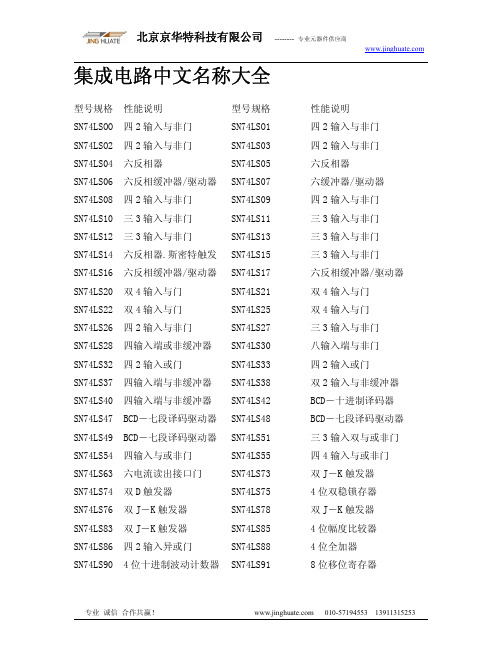
常用数字芯片大全产品型号规格性能说明型号规格性能说明名称74LSSN74LSOO四2输入与非门SN74LSO1四2输入与非门SN74LSO2四2输入与非门SN74LS03四2输入与非门SN74LS04六反相器SN74LS05六反相器SN74LS06六反相缓冲器/驱动器SN74LS07六缓冲器/驱动器SN74LS08四2输入与非门SN74LS09四2输入与非门SN74LS10三3输入与非门SN74LS11三3输入与非门SN74LS12三3输入与非门SN74LS13三3输入与非门SN74LS14六反相器.斯密特触发SN74LS15三3输入与非门SN74LS16六反相缓冲器/驱动器SN74LS17六反相缓冲器/驱动器SN74LS20双4输入与门SN74LS21双4输入与门SN74LS22双4输入与门SN74LS25双4输入与门SN74LS26四2输入与非门SN74LS27三3输入与非门SN74LS28四输入端或非缓冲器SN74LS30八输入端与非门SN74LS32四2输入或门SN74LS33四2输入或门SN74LS37四输入端与非缓冲器SN74LS38双2输入与非缓冲器SN74LS40四输入端与非缓冲器SN74LS42BCD-十进制译码器SN74LS47BCD-七段译码驱动器SN74LS48BCD-七段译码驱动器SN74LS49BCD-七段译码驱动器SN74LS51三3输入双与或非门SN74LS54四输入与或非门SN74LS55四4输入与或非门SN74LS63六电流读出接口门SN74LS73双J-K触发器SN74LS74双D触发器SN74LS754位双稳锁存器SN74LS76双J-K触发器SN74LS78双J-K触发器SN74LS83双J-K触发器SN74LS854位幅度比较器SN74LS86四2输入异或门SN74LS884位全加器SN74LS904位十进制波动计数器SN74LS918位移位寄存器SN74LS9212分频计数器SN74LS93二进制计数器SN74LS965位移位寄存器SN74LS954位并入并出寄存器SN74LS109正沿触发双J-K触发器SN74LS107双J-K触发器SN74LS113双J-K负沿触发器SN74LS112双J-K负沿触发器SN74LS121单稳态多谐振荡器SN74LS114双J-K负沿触发器SN74LS123双稳态多谐振荡器SN74LS122单稳态多谐振荡器SN74LS125三态缓冲器SN74LS124双压控振荡器SN74LS1313-8线译码器SN74LS126四3态总线缓冲器SN74LS13313输入与非门SN74LS132二输入与非触发器SN74LS137地址锁存3-8线译码器SN74LS136四异或门SN74LS139双2-4线译码-转换器SN74LS1383-8线译码/转换器SN74LS14710-4线优先编码器SN74LS145BCD十进制译码/驱动器SN74LS153双4选1数据选择器SN74LS1488-3线优先编码器SN74LS155双2-4线多路分配器SN74LS1518选1数据选择器SN74LS157四2选1数据选择器SN74LS1544-16线多路分配器SN74LS160同步BDC十进制计数器SN74LS156双2-4线多路分配器SN74LS162同步BDC十进制计数器SN74LS158四2选1数据选择器SN74LS1648位串入并出移位寄存SN74LS1614位二进制计数器SN74LS1668位移位寄存器SN74LS1634位二进制计数器SN74LS1694位可逆同步计数器SN74LS1658位移位寄存器SN74LS17216位多通道寄存器堆SN74LS1684位可逆同步计数器SN74LS1746D型触发器SN74LS1704x4位寄存器堆SN74LS176可预置十进制计数器SN74LS1734D型寄存器SN74LS182超前进位发生器SN74LS1754D烯触发器SN74LS18964位随机存储器SN74LS181运算器/函数发生器SN74LS191二进制同步可逆计数器SN74LS183双进位保存全价器SN74LS193二进制可逆计数器SN74LS190同步BCD十进制计数器SN74LS195并行存取移位寄存器SN74LS192BCD-同步可逆计数器SN74LS197可预置二进制计数器SN74LS194双向通用移位寄存器SN74LS2383-8线译码/多路转换器SN74LS196可预置十进制计数器SN74LS241八缓冲/驱动/接收器SN74LS221双单稳态多谐振荡器SN74LS243四总线收发器SN74LS240八缓冲/驱动/接收器SN74LS245八总线收发器SN74LS242四总线收发器SN74LS248BCD-七段译码驱动器SN74LS244八缓冲/驱动/接收器SN74LS251三态8-1数据选择器SN74LS247BCD-七段译码驱动器SN74LS256双四位选址锁存器SN74LS249BCD-七段译码驱动SN74LS258四2选1数据选择器SN74LS253双三态4-1数据选择器SN74LS260双5输入或非门SN74LS257四3态2-1数据选择器SN74LS266四2输入异或非门SN74LS2598位可寻址锁存器SN74LS275七位树型乘法器SN74LS2612x4位二进制乘发器SN74LS279四R-S触发器SN74LS273八进制D型触发器SN74LS2834位二进制全加器SN74LS276四J-K触发器SN74LS2934位二进制计数器SN74LS2809位奇偶数发生校检器SN74LS365六缓冲器带公用启动器SN74LS290十进制计数器SN74LS367六总线三态输出缓冲器SN74LS2954位双向通用移位寄存器SN74LS3738D锁存器SN74LS366六缓冲器带公用启动器SN74LS3754位双稳锁存器SN74LS368六总线三态输出反相器SN74LS386四2输入异或门SN74LS3748D触发器SN74LS393双4位二进制计数器SN74LS3778位单输出D型触发器SN74LS5748位D型触发器SN74LS390双十进制计数器SN74LS6848位数字比较器SN74LS5738位三态输出D型锁存器SN74LS6708位数字比较器产品名称型号规格性能说明产品名称型号规格性能说明7474HCSN7404六反相器SN74HC00四2输入与非门SN7406六反相缓冲器/驱动器SN74HC02四2输入或非门SN7407六缓冲器/驱动器SN74HC03四2输入或非门SN7414六缓冲器/驱动器SN74HC04六反相器SN7416六反相缓冲器/驱动器SN74HC05六反相器SN7440六反相缓冲器/驱动器SN74HC08四2输入与门SN7497六反相缓冲器/驱动器SN74HC10三3输入与非门74F SN74HC11三3输入与门74F00高速四2输入与非门SN74HC14六反相器/斯密特触发74F02高速四2输入或非门SN74HC20双四输入与门74F04高速六反相器SN74HC21双四输入与非门74F08高速四2输入与门SN74HC27三3输入与非门74F10高速三3输入与门SN74HC30八输入端与非门74F14高速六反相斯密特触发SN74HC32四2输入或门74F32高速四2输入或门SN74HC42BCD十进制译码器74F38高速四2输入或门SN74HC73双J-K触的器74F74高速双D型触发器SN74HC74双D型触发器74F86高速四2输入异或门SN74HC76双J-K触的器74F139高速双2-4线译码/驱动器SN74HC86四2输入异或门74F151高速双2-4线译码/驱动器SN74HC107双J-K触发器74F153高速双4选1数据选择器SN74HC113双J-K负沿触发器74F157高速双4选1数据选择器SN74HC123双稳态多谐振荡器74F161高速6D型触发器SN74HC125三态缓冲器74F174高速6D型触发器SN74HC126四三态总线缓冲器74F175高速4D型触发器SN74HC132二输入与非缓冲器74F244高速八总线3态缓冲器SN74HC137二输入与非缓冲器74F245高速八总线收发器SN74HC1383-8线译码/解调器74F373高速8D锁存器SN74HC139双2-4线译码/解调器74HCT SN74HC1488选1数据选择器SN74HCT04六反相器SN74HC151双4选1数据选择器4000SN74HC1544-16线多路分配器CD40014二输入或非门SN74HC157四2选1数据选择器CD4002双4输入或非门SN74HC1614位二进制计数器CD400618位静态移位寄存器SN74HC1634位二进制计数器CD4007双互补对加反相器SN74HC1648位串入并出移位寄存器CD4009六缓冲器/转换-倒相SN74HC1658位移位寄存器CD4010六缓冲器/转换-正相SN74HC1734D型触发器CD4011四2输入与非门SN74HC1746D触发器CD4012双4输入与非门SN74HC1754D型触发器CD4013置/复位双D型触发器SN74HC191二进制同步可逆计数器CD40148位静态同步移位寄存SN74HC221双单稳态多谐振荡器CD4015双4位静态移位寄存器SN74HC2383-8线译码器CD4016四双向模拟数字开关SN74HC240八缓冲器CD401710译码输出十进制计数器SN74HC244八总线3态输出缓冲器CD4018可预置1/N计数器SN74HC245八总线收发器CD4019四与或选择门SN74HC251三态8-1数据选择器CD402014位二进制计数器SN74HC2598位可寻址锁存器CD40218位静态移位寄存器SN74HC266四2输入异或非门CD40228译码输出8进制计数器SN74HC2738D型触发器CD4023三3输入与非门SN74HC367六缓冲器/总线驱动器CD40247位二进制脉冲计数器SN74HC368六缓冲器/总线驱动器CD4025三3输入与非门SN74HC3738D锁存器CD4026十进制/7段译码/驱动SN74HC3748D触发器CD4027置位/复位主从触发器SN74HC393双4位二进制计数器CD4028BCD十进制译码器SN74HC5418位三态输出缓冲器CD40294位可预置可逆计数器SN74HC5738位三态输出D型锁存器CD4030四异或门SN74HC5748D型触发器CD403164位静态移位寄存器SN74HC5958位移位寄存器/锁存器CD4032三串行加法器SN74HC4028 7级二进制串行加数器CD4033十进制计数器/7段显示SN74HC4046 锁相环CD40348位静态移位寄存器SN74HC4050 六同相缓冲器CD40354位并入/并出移位寄存器SN74HC4051 8选1模拟开关CD40383位串行加法器SN74HC4053 三2选1模拟开关CD404012位二进制计数器SN74HC4060 14位计数/分频/振荡器CD4041四原码/补码缓冲器SN74HC4066 四双相模拟开关CD4042四时钟D型锁存器SN74HC4078 3输入端三或门CD4043四或非R/S锁存器SN74HC4511 7段锁存/译码驱动器CD4044四与非R/S锁存器SN74HC4520 双二进制加法计数器产品名称型号规格性能说明产品名称型号规格性能说明4000CD4046锁相环4500CD4047单非稳态多谐振荡器CD4502可选通六反相缓冲器CD4048可扩充八输入门CD4503六同相缓冲器CD4049六反相缓冲/转换器CD4504六电平转换器CD4050六正相缓冲/转换器CD4508双4位锁存器CD4051单8通道多路转换/分配CD4510BCD可预置可逆计数器CD4052双4通道多路转换/分配CD4511BCD7段锁存/译码/驱动CD4053三2通道多路转换/分配CD45128通道数据选择器CD40567段液晶显示译码/驱动CD4513BCD7段锁存/译码/驱动CD4060二进制计数/分频/振荡CD45144-16线译码器CD4063四位数值比较器CD45154-16线译码器CD4066四双相模拟开管CD4518双BCD加法计数器CD406716选1模拟开关CD4520双二进制加法计数器CD40688输入端与非/与门CD452124位分频器CD4069六反相器CD4522可预置BCD1/N计数CD4070四异或门CD4526可预置二进制1/N计数CD4071四2输入或门CD4527BCD系数乘发器CD4072双四输入或门CD4528双单稳态触发器CD4073三3输入与门CD453112位奇偶校验电路CD4075三3输入与门CD45328位优先编码器CD40764位D型寄存器CD4538双精密单稳态触发器CD4077四异或非门CD4539双四路输据选择器CD4078八输入或/或非门CD4541可编程振荡/计时器CD4081四输入与门CD45437段锁存/译码/驱动CD4082双4输入与门CD45533位BCD计数器CD4085双2组2输入与或非门CD4555双4选1译码器CD4086可扩展2输入与或非门CD4556双4选1译码器CD4093四与非斯密特触发器CD45571-64位可变长度寄存器CD40948位移位/贮存总线寄存CD4558BCD-7段译码器CD40963输入J-K触发器CD4560BCD码加法器CD4098双单稳态触发器CD4561BCD转换成9的补码输出CD40998位可寻址锁存器CD4566工业定时基准发生器CD40103同步可预置减法器CD4569双4位可编程1/NBCDCD40106六斯密特触发器CD4583双斯密特触发器CD40107双2输入与非缓冲/驱动CD45844斯密特触发器CD40110计数/译码/锁存/驱动CD45854位数值比较器CD401746D触发器CD45998位总线相容寻址锁存器CD401754D触发器MC145106 频率合成器CD40192BCD可预置可逆计数器MC145026遥控编码器CD40193二进制可预置可逆计数器MC145027译码器CD401944位双相移位寄存器。
74HC373中文资料_数据手册_参数

All information provided in this document is subject to legal disclaimers.
Rev. 6 — 26 February 2016
© NXP Semiconductors N.V. 2016. All rights reserved.
+& +&7
9&& 4 ' ' 4 4 ' ' 4 /(
DDH
Fig 6. Pin configuration SO20, SSOP20 and TSSOP20
WHUPLQDO LQGH[DUHD
4 of 25
NXP Semiconductors
74HC373; 74HCT373
Octal D-type transparent latch; 3-state
6. Functional description
6.1 Function table
Table 3. Function table[1]
Pin 1 2, 5, 6, 9, 12, 15, 16, 19 3, 4, 7, 8, 13, 14, 17, 18 10 11 20
Description 3-state output enable input (active LOW) 3-state latch output data input ground (0 V) latch enable input (active HIGH) supply voltage
3 of 25
NXP Semiconductors
74HC373; 74HCT373
74CD系列芯片功能列表

系列 电平 延迟 电流 AHC CMOS 8.5ns -8/8mA AHCT COMS/TTL 8.5 -8/8 HC COMS 25 -8/8 HCT COMS/TTL 25 -8/8 ACT COMS/TTL 10 -24/24 F TTL 6.5 -15/64 ALS TTL 10 -15/64 LS TTL 18 -15/247400 与非门7401 OC与非门7402 或非门7403 与非门7404 反向器7406 高输出反向器7408 与门7409 OC与门7410 与非门7411 与门74121 单稳态74132 触发器与非门7414 触发器反向器74153 四选一74155 译码器74180 奇偶发生检验74191 计数器7420 双四输入与非门7426 与非门7427 三输入或非门7430 八输入端与非门7432 二输入或门7438 与非门缓冲器7445 译码驱动器7474 D型触发器7475 双锁存器7476 J-K触发器 7485 四位比较器7486 双端异或门74HC74HC00 双输入与非门74HC02 双输入或非门74HC03 与非门74HC04 六路反向器74HC05 六路反向器74HC08 双输入与门74HC107 J-K触发器74HC109A J-K触发器74HC11 三输入与门74HC112 双J-K触发器74HC113 双JK触发器74HC123A 可重触发单稳74HC125 四个三态门74HC126 六三态门74HC132 施密特触发与非门74HC133 十三输入与非门74HC137 3-8线译码器74HC138 3线至8线译码器74HC139 2线至4线译码器74HC14 六触发反向器74HC147 10-4编码器74HC148 8-3编码器74HC149 8-8编码器74HC151 8通道多路器74HC153 双四输入多路器74HC154 4线至16线译码器74HC155 2线至4线译码器74HC157 四个双端多路器74HC161 二进制计数器74HC163 十进制计数器74HC164 串入并出74HC165 并入串出74HC166 串入并出74HC173 三态D触发器74HC174 六D触发器74HC175 六D触发器74HC181 算术逻辑单元74HC182 进位发生器74HC190 二进制加减计数器74HC191 十进制加减计数器74HC192 十进制加减计数器74HC193 二进制加减计数器74HC194 4位双向移位寄存器74HC195 4位并行移位寄存器74HC20 四个四入与非门74HC221 不可重触发单稳74HC237 地址锁3线至8线译码器74HC242/243 三态收发器74HC244 八个三态缓冲门74HC245 三态收发器74HC251 8路3态多路器74HC253 4路3态多路器74HC257 4路3态多路器74HC258 2路3态多路器74HC259 8位地址锁存译码器74HC266A 异或非74HC27 3输入或非门74HC273 8路D触发器74HC280 奇偶发生器74HC283 四位加法器74HC299 三态移位寄存74HC30 8输入端与非门74HC32 四个双端或门74HC34 非反向器74HC354 8路3态多路器74HC356 8路3态多路器74HC365 六个三态缓冲门74HC366 缓冲反向器74HC367 缓冲反向器74HC368 缓冲反向器74HC373 三态D型锁存器- 1 -74HC374 三态D触发器74HC393 4位二进制计数器74HC4016 四路模拟量开关74HC4020 14输出计数器74HC4017 十进制计数10译码输出端 74HC4040 12出计数器74HC4046 相位监测输出器74HC4049 电平变低器74HC4050 电平变低器74HC4051 8通道多路器74HC4052 4通道多路器74HC4053 2通道多路器74HC4060 14阶BIN计数74HC4066 四通道多路器74HC4075 3输入或门74HC42 BCD转十进制译码器74HC423A 可重触发单稳74HC4511 7段译码器74HC4514 4至16线译码器74HC4538A 可重触发单稳74HC4543 LCD用BCD-7段译码74HC51 与或非门74HC521 判决定路74HC533 三态D锁存器74HC534 三态D型触发器74HC540 三态缓冲器74HC541 三态缓冲反向器74HC58 与或门74HC589 8位移位寄存三态输出 74HC594 8位移位寄存器74HC595 8位移位寄存器出锁存 74HC597 8位移位寄存器入锁存 74HC620 反向3态收发器74HC623 八路三态收发器74HC640 反向3态收发器74HC643 八路三态收发器74HC646 总线收发器74HC648 反向总线收发器 74HC688 8位判决电路74HC7266 异或非门74HC73 双JK触发器74HC74A 双D触发器74HC75 4位双稳锁存器74HC76 双JK触发器74HC85 4位判决电路74HC86 2输入异或门74HC942 300BPS低速调制解调器74HC943 300BPS低速调制解调器74LS74LS00 与非门74LS02 或非门74LS03 与非门74LS04 反向器74LS05 六路反向器74LS08 与门74LS09 OC与门74LS10 与非门74LS109 与门74LS11 与门74LS112 双J-K触发器74LS113 双JK触发器74LS114 负沿J-K触发器74LS122 可重触发单稳74LS123 可重触发单稳74LS125 四个三态门74LS13 4输入与非触发器74LS160 计数器74LS136 异或门74LS138 3线至8线译码器74LS139 2线至4线译码器74LS14 六触发反向器74HC147 10-4编码器74HC148 8-3编码器74HC149 8-8编码器74LS151 8通道多路器74LS153 双四输入多路器74LS155 2线至4线译码器74LS156 2-4译码器74LS157 四个双端多路器74LS158 2-1线多路器74LS160A 二进制计数器74LS161A 二进制计数器74LS162A 二进制计数器74LS163A 十进制计数器74LS164 串入并出74LS168 双向计数器74LS169 四位加减计数器74LS173 三态D触发器74LS174 六D触发器74LS175 六D触发器74LS190 二进制加减计数器74LS191 十进制加减计数器74LS192 十进制加减计数器74LS193 二进制加减计数器74LS194A 4位双向移位寄存器74LS195A 4位并行移位寄存器74LS20 四个四入与非门74LS21 四输入端与门74LS240 八个三态缓冲门74LS244 八个三态缓冲门74LS245 三态收发器74LS253 4路3态多路器74LS256 四位可锁存锁存器74LS257 4路3态多路器74LS258 2路3态多路器74LS27 三输入或非门74LS279 四个RS非锁存器74LS28 四双端或非缓冲74LS283 四位加法器74LS30 八输入端与非门74LS32 二输入或门74LS352 4-1线选择多路器74LS365 六个三态缓冲门74LS367 缓冲反向器- 2 -- 3 -74LS368 缓冲反向器 74LS373 三态输出锁存器 74LS76 2个JK 触发器 74LS379 四个并行寄存器 74LS38 与非门缓冲器 74LS390 2个10进制计数器 74LS393 2个2进制计数器 74LS42 BCD 转十进制译码器 74LS48 BCD-7段译码器 74LS49 BCD-7段译码器 74LS51 与或非门 74LS540 8路缓冲驱动器 74LS541 8路缓冲驱动器 74LS74 D 型触发器 74LS682 8路比较器 74LS684 8路比较器 74LS75 双锁存器 74LS83A 四位加法器 74LS85 4位判决电路 74LS86 2输入异或门 74LS90 十/二进制计数器 74LS95B 4位左右移位寄存 74LS688 8位判决电路 74LS136 2输入异或门 74LS651 总线收发器 74LS653 总线收发器 74LS670 3态4-4寄存器 74LS73A 双JK 触发器CD 系列门电路 CD4000 双3输入端或非门 CD4001 四2输入端或非门 CD4002 双4输入端或非门 CD4007 双互补对加反向器 CD4009 六反向缓冲/变换器 CD4011 四2输入端与非门 CD4012 双4输入端与非门 CD4023 三2输入端与非门 CD4025 三2输入端与非门CD4030 四2输入端异或门 CD4041 四同相/反向缓冲器 CD4048 8输入端可扩展多功能门 CD4049 六反相缓冲/变换器 CD4050 六同相缓冲/变换器 CD4068 8输入端与门/与非门 CD4069 六反相器 CD4070 四2输入异或门 CD4071 四2输入端或门 CD4072 双4输入端或门 CD4073 三3输入端与门 CD4075 三3输入端或门 CD4077 四异或非门CD4078 8输入端与非门/或门 CD4081 四2输入端与门 CD4082 双4输入端与非门 CD4085 双2路2输入端与或非门 CD4086 四2输入端可扩展与或非门 CD40104 TTL 至高电平CMOS 转换器 CD40106 六施密特触发器CD40107 双2输入端与非缓冲/驱动 CD40109 四低-高电平位移器 CD4501 三多输入门CD4052 六反向缓冲器(三态输出) CD4503 六同相缓冲器(三态输出) CD4504 6TTL 或CMOS 同级移相器 CD4506 双可扩展AIO 门 CD4507 四异或门CD4519 4位与/或选择器 CD4530 双5输入多数逻辑门 CD4572 四反向器\二输入或非门 CD4599 8 位可寻址锁存器触发器 CD4013 双D 触发器 CD4027 双JK 触发器 CD4042 四锁存D 型触发器 CD4043 四三态R-S 锁存触发器 CD4044 四三态R-S 锁存触发器CD4047 单稳态触发/无稳多谐振荡器 CD4093 四2输入端施密特触发器 CD4098 双单稳态触发器 CD4099 8位可寻址锁存器 CD4508 双4位锁存触发器 CD4528 双单稳态触发器 CD4538 精密单稳多谐振荡器 CD4583 双施密特触发器 CD4584 六施密特触发器 CD4599 8位可寻址锁存器计数器CD4017 十进制计数/分配器 CD4020 14位二进制串行计数器 CD4022 八进制计数/分配器 CD4024 7位二进制串行计数器/分频 CD4029 预置数可逆计数器 CD4040 12二进制串行计数器 CD4045 12位计数/缓冲器 CD4059 四十进制N 分频器 CD4060 14二进制串行计数器/分频 CD4095 3输入端J-K 触发器 CD4096 3输入端J-K 触发器 CD40110 十进制加减计数/7端译码 CD40160 可预置数BCD 加计数器 CD40161 可预置数4位二进制加计数器 CD40162 可预置数BCD 加计数器 CD40163 可预置数4位二进制加计数器 CD40192 可预置数BCD 加/减计数器 CD40193 可预置4位二进制加/减计数 CD4510 可预置BCD 加/减计数器 CD4516 可预置4位二进制加/减计数 CD4518 双BCD 同步加计数器CD4520 双同步4位二进制加计数器CD4521 24级频率分频器CD4522 可预置BCD 同步1/N 加计数器 CD4526 4位二进制同步1/N 加计数器 CD4534 实时与译码计数器 CD4536 可编程定时器- 4 -CD4541 可编程定时器 CD4553 3数字BCD 计数器CD4568 相位比较器/可编程计数器 CD4569 双可预置BCD/二进制计数器 CD4597 8位总线相容计数/锁存器 CD4598 8位总线相容可建地址锁存器译码器 CD4511 BCD 锁存/7段译码器/驱动器 CD4514 4位锁存/4-16线译码器 CD4515 4位锁存/4-16线译码器 CD4026 十进制计数/7段译码器 CD4028 BCD-十进制译码器 CD4033 十进制计数/7段译码器 CD4054 4位液晶显示驱动 CD4055 BCD-7段码/液晶驱动 CD4056 BCD-7段码/驱动CD40102 8位同步减法计时器(BCD) CD40103 8位同步减法计时器(二进制) CD4513 BCD-锁存/7端译码/驱动器 CD4514 4位锁存/4线—16线译码器 CD4515 4位锁存/4线—16线译码器 CD4543 BCD-锁存/7段译码/驱动器 CD4544 BCD-锁存/7段译码波动闭锁 CD4547 BCD-锁存/7段译码/大电流 CD4555 双二进制4选1译码器/分离 CD4556 双二进制4选1译码器/分离 CD4558 BCD-7段译码CD4555 双二进制4选1译码器/分离器 CD4556 双二进制4选1译码器/分离器移位寄存器 CD4006 18位串入—串出移位寄存器 CD4014 8位串入/并入—串出移位 CD4015 双4位串入—并出移位寄存器 CD4021 8位串入/并入—串出移位 CD4031 64位移位寄存器 CD4034 8位通用总线寄存器 CD4035 4位串/并入—串/并出移位 CD4076 4线D 型寄存器CD4094 8位移位/存储总线寄存器CD40100 32位左移/右移 CD40105 先进先出寄存器 CD40108 4×4多端口寄存器阵列 CD40194 4位并/串入—并/串出移位 CD40195 4位并/串入—并/串出移位 CD4517 64位移位寄存器 CD45490 连续的近似值寄存器 CD4562 128位静态移位寄存器 CD4580 4×4多端寄存器模拟开关和数据选择器 CD4016 四联双向开关 CD4019 四与或选择器 CD4051 单八路模拟开关 CD4052 双4路模拟开关 CD4053 三2路模拟开关 CD4066 四双向模拟开关 CD4067 单十六路模拟开关 CD4097 双八路模拟开关 CD40257 四2选1数据选择器 CD4512 八路数据选择器 CD4529 双四路/单八路模拟开关 CD4539 双四路数据选择器CD4551 四2通道模拟多路传输运算电路 CD4008 4位超前进位全加器CD4019 四与或选择器 CD4527 BCD 比例乘法器 CD4032 三路串联加法器CD4038 三路串联加法器(负逻辑) CD4063 四位量级比较器 CD4070 四2输入异或门 CD4585 4位数值比较器 CD4089 4位二进制比例乘法器 CD40101 9位奇偶发生器/校验器 CD4527 BCD 比例乘法器 CD4531 12位奇偶数 CD4559 逐次近似值码器 CD4560 “N”BCD 加法器 CD4561 “9”求补器 CD4581 4位算术逻辑单元 CD4582 超前进位发生器CD4585 4位数值比较器存储器CD4049 4字×8位随机存取存储器 CD4505 64×1位RAMCD4537 256×1静态随机存取存储器 CD4552 256位RAM特殊电路CD4046 锁相环集成电路 CD4532 8位优先编码器 CD4500 工业控制单元 CD4566 工业时基发生器 CD4573 可预置运算放大器 CD4574 比较器、线性、双对双运放 CD4575 双/双预置运放/比较器CD4597 8位总线相容计数/锁存器 CD4598 8位总线相容可建地址。
集成电路IC芯片中文名称大全
专业 诚信 合作共赢!
010-57194553 13911315253
北京京华特科技有限公司 -------- 专业元器件供应商
SN7407 六缓冲器/驱动器
SN74HC03
SN7414 六缓冲器/驱动器
SN74HC04
SN7416 六反相缓冲器/驱动器 SN74HC05
SN74LS126
SN74LS133 13 输入与非门
SN74LS132
SN74LS137 地址锁存 3-8 线译码器 SN74LS136
SN74LS139 双 2-4 线译码-转换器 SN74LS138
SN74LS147 10-4 线优先编码器 SN74LS145
SN74LS153 双 4 选 1 数据选择器 SN74LS148
专业 诚信 合作共赢!
010-57194553 13911315253
北京京华特科技有限公司 -------- 专业元器件供应商
SN74LS92 12 分频计数器
SN74LS93
SN74LS96 5 位移位寄存器
SN74LS95
SN74LS273
SN74LS283 4 位二进制全加器
SN74LS276
SN74LS293 4 位二进制计数器
SN74LS280
SN74LS365 六缓冲器带公用启动器 SN74LS290
SN74LS367 六总线三态输出缓冲器 SN74LS295
SN74LS373 8D 锁存器 SN74LS375 4 位双稳锁存器 SN74LS386 四 2 输入异或门 SN74LS393 双 4 位二进制计数器 SN74LS574 8 位 D 型触发器
SN74LS155 双 2-4 线多路分配器 SN74LS151
74HC系列资料查询

7474HC4052 74HC4053 74HC4060 74HC4066 74HC4075 74HC42 74HC423A 74HC4514 74HC4538A 74HC4543 74HC51 74HC521 74HC533 74HC534 74HC540 74HC541 74HC58 74HC589 74HC594 74HC595 74HC597 74HC620 74HC623 74HC640 74HC643 74HC646 74HC648 74HC688 74HC7266 74HC73 74HC74A 74HC75 74HC76 74HC85 74HC86 74HC942 74HC943 74LS00 74LS02 74LS03 74LS04 74LS05 74LS08 74LS09 74LS10 74LS109 74LS11 74LS112 74LS113 74LS114 74LS122 74LS123 74LS125 74LS160 74LS136 74LS138 74LS139 74LS14 74HC147 74HC148 74HC149 74LS151 74LS153 74LS155 74LS156 74LS157 74LS158 74LS160A 74LS161A 74LS162A 74LS163A 74LS164 74LS168 74LS169 74LS173 74LS174 74LS175 74LS190 74LS191 74LS192 74LS193 74LS194A 74LS195A 74LS20 74LS21 74LS240 74LS244 74LS245 74LS253 74LS256 74LS257 74LS258 74LS27 74LS279 74LS28 74LS283 74LS30 74LS32 74LS352 74LS367 74LS368A 74LS373 74LS76 74LS379 74LS38 74LS390 74LS393 74LS42 74LS48 74LS49 74LS51 74LS540 74LS541 74LS74 74LS682 74LS684 74LS75 74LS83A 74LS85 74LS86 74LS90 74LS95B 74LS688 74LS136 4000与4500系列型号规格性能说明CD4000 "3输入双或非门1反相器"CD4001 "四2输入或非门"CD4002 "双4输入或非门"CD4006 "18级静态移位寄存器"CD4007 "双互补对加反相器"CD4008 "4位二进制并行进位全加器"CD4009 "六缓冲器/转换器(反相)"CD4010 "六缓冲器/转换器(同相)"CD40100 "32位双向静态移位寄存器"CD40101 "9位奇偶发生器/校验器"CD40102 "8位BCD可预置同步减法计数器"CD40103 "8位二进制可预置同步减法计数器"CD40104 "4位三态输出双向通用移位寄存器"CD40105 "先进先出寄存器"CD40106 "六施密特触发器"CD40107 "2输入双与非缓冲/驱动器"CD40108 "4×4多端寄存"CD40109 "四三态输出低到高电平移位器" CD4011 "四2输入与非门"CD40110 "十进制加减计数/译码/锁存/驱动" CD40117 "10线—4线BCD优先编码器"CD4012 "双4输入与非门"CD4013 "带置位/复位的双D触发器"CD4014 "8级同步并入串入/串出移位寄存器" CD40147 "10线—4线BCD优先编码器"CD4015 "双4位串入/并出移位寄存器"CD4016 "四双向开关"CD40160 "非同步复位可预置BCD计数器" CD40161 "非同步复位可预置二进制计数器" CD40162 "同步复位可预置BCD计数器"CD40163 "同步复位可预置二进制计数器" CD4017 "十进制计数器/分频器"CD40174 "六D触发器"CD40175 "四D触发器"CD4018 可预置1/N计数器CD40181 "4位算术逻辑单元"CD40182 "超前进位发生器"CD4019 "四与或选译门"CD40192 "可预制四位BCD计数器"CD40193 "可预制四位二进制计数器"CD40194 "4位双向并行存取通用移位寄存器" CD4020 "14级二进制串行计数/分频器"CD40208 "4×4多端寄存器"CD4021 "异步8位并入同步串入/串出寄存器" CD4022 "八进制计数器/分频器"CD4023 "三3输入与非门"CD4024 "7级二进制计数器"CD4025 "三3输入或非门"CD40257 "四2线-1线数据选择器/多路传输" CD4026 "7段显示十进制计数/分频器"CD4027 "带置位复位双J-K主从触发器"CD4028 BCD-十进制译码器CD4029 "可预制加/减(十/二进制)计数器" CD4030 "四异或门"CD4031 "64级静态移位寄存器"CD4032 "3位正逻辑串行加法器"CD4033 "十进制计数器/消隐7段显示"CD4034 "8位双向并、串入/并出寄存器"CD4035 "4位并入/并出移位寄存器"CD4038 "3位串行负逻辑加法器"CD40CD40 "12级二进制计数/分频器"CD4041 "四原码/补码缓冲器"CD4042 四时钟控制D锁存器CD4043 四三态或非R/S锁存器CD4044 四三态与非R/S锁存器CD4045 "21位计数器"CD4046 PLL锁相环电路CD4047 "单稳态、无稳态多谐振荡器"CD4048 "8输入端多功能可扩展三态门" CD4049 "六反相缓冲器/转换器"CD4050 "六同相缓冲器/转换器"CD4051 "8选1双向模拟开关"CD4052 "双4选1双向模拟开关"CD4053 "三2选1双向模拟开关"CD4054 "四位液晶显示驱动器"CD4055 "BCD—7段译码/液晶显示驱动器" CD4056 "BCD—7段译码/驱动器"CD4059 可编程1/N计数器CD4060 "14级二进制计数/分频/振荡器" CD4063 "四位数字比较器"CD4066 "四双向模拟开关"CD4067 "单16通道模拟开关"CD4068 "8输入端与非门"CD4069 "六反相器"CD4070 "四异或门"CD4071 "四2输入端或门"CD4072 "4输入端双或门"CD4073 "3输入端三与门"CD4075 "3输入端三或门"CD4076 "4位三态输出D寄存器"CD4077 "四异或非门"CD4078 "8输入端或非门"CD4081 "四2输入端与门"CD4082 "4输入端双与门"CD4085 "双2×2与或非门"CD4086 "2输入端可扩展四与或非门"CD4089 "二进制系数乘法器"CD4093 "四2输入端施密特触发器"CD4094 "8级移位存储总线寄存器"CD4095 "选通J-K同相输入主从触发器" CD4096 "选通J-K反相输入主从触发器" CD4097 "双8通道模拟开关"CD4098 "双单稳态多谐振荡器"CD4099 "八位可寻址锁存器7400 "2输入端四与非门"7401 "集电极开路2输入端四与非门" 7402 "2输入端四或非门"7403 "集电极开路2输入端四与非门" 7404 "六反相器"7405 "集电极开路六反相器"7406 "集电极开路六反相高压驱动器" 7407 集电极开路六正相高压驱动器7408 "2输入端四与门"7409 集电极开路2输入端四与门7410 "3输入端3与非门"74107 "带清除主从双J-K触发器"74109 "带预置清除正触发双J-K触发器" 7411 "3输入端3与门"74112 "带预置清除负触发双J-K触发器" 7412 "开路输出3输入端三与非门"74121 "单稳态多谐振荡器"74122 "可再触发单稳态多谐振荡器" 74123 "双可再触发单稳态多谐振荡器" 74125 "三态输出高有效四总线缓冲门" 74126 "三态输出低有效四总线缓冲门" 7413 "4输入端双与非施密特触发器" 74132 "2输入端四与非施密特触发器" 74133 "13输入端与非门"74136 "四异或门"74138 "3-8线译码器/复工器"74139 "双2-4线译码器/复工器"7414 "六反相施密特触发器"74145 "BCD—十进制译码/驱动器"7415 "开路输出3输入端三与门"74150 "16选1数据选择/多路开关" 74151 "8选1数据选择器"74153 "双4选1数据选择器"74154 "4线—16线译码器"74155 "图腾柱输出译码器/分配器" 74156 "开路输出译码器/分配器"74157 "同相输出四2选1数据选择器" 74158 "反相输出四2选1数据选择器" 7416 "开路输出六反相缓冲/驱动器" 74160 "可预置BCD异步清除计数器" 74161 "可予制四位二进制异步清除计数器" 74162 "可预置BCD同步清除计数器" 74163 "可予制四位二进制同步清除计数器" 74164 "八位串行入/并行输出移位寄存器" 74165 "八位并行入/串行输出移位寄存器" 74166 "八位并入/串出移位寄存器" 74169 "二进制四位加/减同步计数器" 7417 "开路输出六同相缓冲/驱动器" 74170 "开路输出4×4寄存器堆"74173 "三态输出四位D型寄存器"74174 "带公共时钟和复位六D触发器" 74175 "带公共时钟和复位四D触发器" 74180 "9位奇数/偶数发生器/校验器" 74181 "算术逻辑单元/函数发生器"74185 "二进制—BCD代码转换器"74190 "BCD同步加/减计数器"74191 "二进制同步可逆计数器"74192 "可预置BCD双时钟可逆计数器" 74193 "可预置四位二进制双时钟可逆计数器" 74194 "四位双向通用移位寄存器"74195 "四位并行通道移位寄存器"74196 "十进制/二-十进制可预置计数锁存器" 74197 "二进制可预置锁存器/计数器"7420 "4输入端双与非门"7421 "4输入端双与门"7422 "开路输出4输入端双与非门"74221 "双/单稳态多谐振荡器"74240 "八反相三态缓冲器/线驱动器" 74241 "八同相三态缓冲器/线驱动器" 74243 "四同相三态总线收发器"74244 "八同相三态缓冲器/线驱动器" 74245 "八同相三态总线收发器"74247 "BCD—7段15V输出译码/驱动器" 74248 "BCD—7段译码/升压输出驱动器" 74249 "BCD—7段译码/开路输出驱动器" 74251 "三态输出8选1数据选择器/复工器" 74253 "三态输出双4选1数据选择器/复工器" 74256 "双四位可寻址锁存器"74257 "三态原码四2选1数据选择器/复工器" 74258 "三态反码四2选1数据选择器/复工器" 74259 "八位可寻址锁存器/3-8线译码器" 7426 "2输入端高压接口四与非门"74260 "5输入端双或非门"74266 "2输入端四异或非门"7427 "3输入端三或非门"74273 "带公共时钟复位八D触发器"74279 "四图腾柱输出S-R锁存器"7428 "2输入端四或非门缓冲器"74283 "4位二进制全加器"74290 "二/五分频十进制计数器"74293 "二/八分频四位二进制计数器" 74295 "四位双向通用移位寄存器"74298 "四2输入多路带存贮开关"74299 "三态输出八位通用移位寄存器" 7430 "8输入端与非门"7432 "2输入端四或门"74322 "带符号扩展端八位移位寄存器"74323 "三态输出八位双向移位/存贮寄存器" 7433 "开路输出2输入端四或非缓冲器" 74347 "BCD—7段译码器/驱动器"74352 "双4选1数据选择器/复工器"74353 "三态输出双4选1数据选择器/复工器" 74365 "门使能输入三态输出六同相线驱动器" 74366 "门使能输入三态输出六反相线驱动器" 74367 "4/2线使能输入三态六同相线驱动器" 74368 "4/2线使能输入三态六反相线驱动器" 7437 "开路输出2输入端四与非缓冲器" 74373 "三态同相八D锁存器"74374 "三态反相八D锁存器"74375 "4位双稳态锁存器"74377 "单边输出公共使能八D锁存器" 74378 "单边输出公共使能六D锁存器" 74379 "双边输出公共使能四D锁存器"7438 "开路输出2输入端四与非缓冲器" 74380 "多功能八进制寄存器"7439 "开路输出2输入端四与非缓冲器" 74390 "双十进制计数器"74393 "双四位二进制计数器"7440 "4输入端双与非缓冲器"7442 "BCD—十进制代码转换器"74447 "BCD—7段译码器/驱动器"7445 "BCD—十进制代码转换/驱动器" 74450 "16:1多路转接复用器多工器" 74451 "双8:1多路转接复用器多工器" 74453 "四4:1多路转接复用器多工器"7446 "BCD—7段低有效译码/驱动器" 74460 "十位比较器"74461 "八进制计数器"74465 "三态同相2与使能端八总线缓冲器" 74466 "三态反相2与使能八总线缓冲器" 74467 "三态同相2使能端八总线缓冲器" 74468 "三态反相2使能端八总线缓冲器" 74469 "八位双向计数器"7447 "BCD—7段高有效译码/驱动器"7448 "BCD—7段译码器/内部上拉输出驱动" 74490 "双十进制计数器"74491 "十位计数器"74498 "八进制移位寄存器"7450 "2-3/2-2输入端双与或非门"74502 "八位逐次逼近寄存器"74503 "八位逐次逼近寄存器"7451 "2-3/2-2输入端双与或非门"74533 "三态反相八D锁存器"74534 "三态反相八D锁存器"7454 "四路输入与或非门"74540 "八位三态反相输出总线缓冲器" 7455 "4输入端二路输入与或非门" 74563 "八位三态反相输出触发器" 74564 "八位三态反相输出D触发器" 74573 "八位三态输出触发器"74574 "八位三态输出D触发器"74645 "三态输出八同相总线传送接收器" 74670 "三态输出4×4寄存器堆"7473 "带清除负触发双J-K触发器" 7474 "带置位复位正触发双D触发器" 7476 "带预置清除双J-K触发器"7483 "四位二进制快速进位全加器" 7485 "四位数字比较器"7486 "2输入端四异或门"7490 "可二/五分频十进制计数器"7493 "可二/八分频二进制计数器"7495 "四位并行输入输出移位寄存器" 7497 "6位同步二进制乘法器"74、74HC、74LS系列芯片资料2006-9-22 23:06系列 电平 典型传输延迟ns 最大驱动电流(-Ioh/Lol)mA AHC CMOS 8.5 -8/8AHCT COMS/TTL 8.5 -8/8HC COMS 25 -8/8HCT COMS/TTL 25 -8/8ACT COMS/TTL 10 -24/24F TTL 6.5 -15/64ALS TTL 10 -15/64LS TTL 18 -15/24注:同型号的74系列、74HC系列、74LS系列芯片,逻辑功能上是一样的。
客房智能控制系统使用说明

客房智能控制系统使用说明书2007年03月27日目录第一章客房控制设备使用说明 31、客房灯光控制 (3)2、客房插座电源控制 (3)3、客房空调控制 (3)4、客房服务信息控制 (4)第二章客房管理软件使用说明 41、服务器系统及数据库建立 (5)2、客房控制系统数据库导入步骤: (6)3、客房管理软件使用说明 (7)4、网络控制器参数设置及使用说明 (21)第三章常见电子元器件参数及维修211、常用主要的元器件 (21)2、AIO CHJR板主要元器件的作用 (23)3、AIO CHMAN主要元器件的作用 (25)4、16PKZ板主要元器件的作用 (29)5、常见故障及排除方法: (31)6、网络硬件常见故障 (40)第四章附图421、接线端子表 (42)2、网络拓朴图 (42)3、系统示意图 (42)4、控制原理图 (42)5、开关接线图 (42)第一章客房控制设备使用说明1、客房灯光控制廊灯:由门磁开关和墙面开关双点控制。
打开房门,不论白天或夜间,廊灯均自动点亮;如不插入有效房卡,且不关房门,则廊灯一直亮;如不插入有效房卡,而关闭房门,则廊灯延时2分钟关闭;如插入有效房卡,且关闭房门,则廊灯一直亮,客人可按动廊灯开关关闭或打开廊灯。
卫生间灯光:由卫生间红外开关与墙面开关双点控制①卫生间灯:插入有效房卡后,系统从待机模式转入工作模式,按卫生间灯开关,可以打开或关闭卫生间灯;按动总开关,可关闭已经打开的卫生间灯;当红外线感应到卫生间无人时,延时15分钟关闭卫生间灯。
②防雾灯与排风扇:插入有效房卡后,系统从待机模式转入工作模式,按动排风扇与防雾灯开关,可以打开或关闭排风扇与防雾灯;当卫生间红外线感应到有人进入卫生间时,打开排气扇与防雾灯;按动总开关,可关闭已经打开的排风扇与防雾灯;当红外线感应到卫生间无人时,延时15分钟关闭排气扇与防雾灯。
左、右床灯:可控硅对左右床灯(仅限白炽灯)无级调光。
点按左、右床灯开关,左右床灯亮100%亮度,再次点按左、右床灯开关,左右床灯关闭;按住左、右床灯开关,左、右床灯从关闭逐渐至100%亮度,再按住左、右床灯开关,左、右床灯灯光亮度减少,直至关闭;持续按住左、右床灯开关调光过程中,松开左、右床灯调光开关,则左、右床灯停在当前亮度;按动总开关,可关闭已经打开的左、右床灯。
74HC373中文资料

74HC373和74LS373原理一样,8数据锁存器。
主要用于数码管、按键等等的控制1. 真值表Dn LE OE OnH H L HL H L LX L L QoX X H Z这个就是真值表,表示这个芯片在输入和其它的情况下的输出情况。
每个芯片的数据手册(datasheet)中都有真值表。
布尔逻辑比较简单,在此不赘述;2. 高阻态就是输出既不是高电平,也不是低电平,而是高阻抗的状态;在这种状态下,可以多个芯片并联输出;但是,这些芯片中只能有一个处于非高阻态状态,否则会将芯片烧毁; 高阻态的概念在RS232和RS422通讯中还可以用到。
3. 数据锁存当输入的数据消失时,在芯片的输出端,数据仍然保持;这个概念在并行数据扩展中经常使用到。
4. 数据缓冲加强驱动能力。
74LS244/74LS245/74LS373/74LS573都具备数据缓冲的能力。
OE:output_enable,输出使能;LE:latch_enable,数据锁存使能,latch是锁存的意思;Dn:第n路输入数据;On:第n路输出数据;再看这个真值表,意思如下:第四行:当OE=1是,无论Dn、LE为何,输出端为高阻态;第三行:当OE=0、LE=0时,输出端保持不变;第二行第一行:当OE=0、LE=1时,输出端数据等于输入端数据;结合下面的波形图,在实际应用的时候是这样做的:a.OE=0;b.先将数据从单片机的口线上输出到Dn;c.再将LE从0->1->0d.这时,你所需要输出的数据就锁存在On上了,输入的数据在变化也影响不到输出的数据了;实际上,单片机现在在忙着干别的事情,串行通信、扫描键盘……单片机的资源有限啊。
在单片机按照RAM方式进行并行数据的扩展时,使用movx @dptr, A这条指令时,这些时序是由单片机来实现的。
后面的表格中还有需要时间的参数,你不需要去管它,因为这些参数都是几十ns级别的,对于单片机在12M下的每个指令周期最小是1us的情况下,完全可以实现;如果是你自己来实现这个逻辑,类似的指令如下:mov P0,A ;将数据输出到并行数据端口clr LEsetb LEclr LE ;上面三条指令完成LE的波形从0->1->0的变化74ls573跟74LS373逻辑上完全一样,只不过是管脚定义不一样,数据输入和输出端。
74HC373及74HCT373规格书

74HC373; 74HCT373Octal D-type transparent latch; 3-stateRev. 4 — 3 September 2010Product data sheet1. General descriptionThe 74HC373; 74HCT373 is a high-speed Si-gate CMOS device and is pin compatiblewith Low-power Schottky TTL. It is specified in compliance with JEDEC standard no. 7A.The 74HC373; 74HCT373 is an octal D-type transparent latch featuring separate D-typeinputs for each latch and 3-state outputs for bus oriented applications. A latch enable (LE)input and an output enable (OE) input are common to all latches.The 74HC373; 74HCT373 consists of eight D-type transparent latches with 3-state trueoutputs. When LE is HIGH, data at the Dn inputs enters the latches. In this condition thelatches are transparent, i.e. a latch output will change state each time its correspondingD input changes.When LE is LOW the latches store the information that was present at the D inputs aset-up time preceding the HIGH-to-LOW transition of LE. When OE is LOW, the contentsof the 8 latches are available at the outputs. When OE is HIGH, the outputs go to the high-impedance OFF-state. Operation of the OE input does not affect the state of the latches.The 74HC373; 74HCT373 is functionally identical to:•74HC563; 74HCT563: but inverted outputs and different pin arrangement•74HC573; 74HCT573: but different pin arrangement2. Features and benefits3-state non-inverting outputs for bus oriented applicationsCommon 3-state output enable inputFunctionally identical to the 74HC563; 74HCT563 and 74HC573; 74HCT573ESD protection:HBM JESD22-A114F exceeds 2000VMM JESD22-A115-A exceeds 200VSpecified from −40°C to+85°C and from −40°C to+125°C3. Ordering information4. Functional diagramTable 1.Ordering informationType number PackageTemperature rangeName DescriptionVersion 74HC373N −40°C to +125°CDIP20plastic dual in-line package; 20leads (300mil)SOT146-174HCT373N 74HC373D −40°C to +125°CSO20plastic small outline package; 20leads;body width 7.5mmSOT163-174HCT373D 74HC373DB −40°C to +125°CSSOP20plastic shrink small outline package; 20leads; body width 5.3mmSOT339-174HCT373DB 74HC373PW −40°C to +125°CTSSOP20plastic thin shrink small outline package; 20leads; body width 4.4mmSOT360-174HCT373PW 74HC373BQ −40°C to +125°CDHVQFN20plastic dual in-line compatible thermal enhanced very thin quad flat package; no leads; 20terminals; body 2.5×4.5×0.85mmSOT764-174HCT373BQ5. Pinning information5.1Pinning5.2Pin descriptionTable 2.Pin descriptionSymbol Pin DescriptionOE13-state output enable input (active LOW) Q0, Q1, Q2, Q3, Q4, Q5, Q6, Q72, 5, 6, 9, 12, 15, 16, 193-state latch outputD0, D1, D2, D3, D4, D5, D6, D73, 4, 7, 8, 13, 14, 17, 18data inputGND10ground (0V)LE11latch enable input (active HIGH)V CC20supply voltage6. Functional description6.1Function table[1]H =HIGH voltage level;h =HIGH voltage level one set-up time prior to the HIGH-to-LOW LE transition;L =LOW voltage level;I =LOW voltage level one set-up time prior to the HIGH-to-LOW LE transition;X =don’t care;Z = high-impedance OFF-state.7. Limiting values[1]For DIP20 package: P tot derates linearly with 12mW/K above 70°C.[2]For SO20: P tot derates linearly with 8mW/K above 70°C.[3]For SSOP20 and TSSOP20 packages: P tot derates linearly with 5.5mW/K above 60°C.[4]For DHVQFN20 package: P tot derates linearly with 4.5mW/K above 60°C.Table 3.Function table [1]Operating mode Control Input Internal latches Output OE LE Dn Qn Enable and read register (transparent mode)L H L L L H H H Latch and read register L L l L L h H H Latch register and disable outputsHXXXZTable 4.Limiting valuesIn accordance with the Absolute Maximum Rating System (IEC 60134). Voltages are referenced to GND (ground = 0 V).Symbol Parameter ConditionsMin Max Unit V CC supply voltage −0.5+7V I IK input clamping current V I < −0.5V or V I >V CC +0.5 V -±20mA I OK output clamping current V O <−0.5V or V O >V CC +0.5V -±20mA I O output current V O = −0.5V to (V CC +0.5V)-±35mA I CC supply current -+70mA I GND ground current -−70mA T stg storage temperature −65+150°C P tottotal power dissipationDIP20 package [1]-750mW SO20 package [2]-500mW SSOP20 package [3]500mW TSSOP20 package [3]500mW DHVQFN20 package[4]-500mW8. Recommended operating conditions9. Static characteristicsTable 5.Recommended operating conditions Voltages are referenced to GND (ground = 0V)Symbol Parameter Conditions74HC37374HCT373UnitMin Typ Max Min Typ Max V CC supply voltage 2.0 5.0 6.0 4.5 5.0 5.5V V I input voltage 0-V CC 0-V CC V V O output voltage 0-V CC 0-V CC V T amb ambient temperature−40+25+125−40+25+125°C Δt/ΔVinput transition rise and fall rateV CC = 2.0 V --625---ns/V V CC = 4.5 V - 1.67139- 1.67139ns/V V CC = 6.0 V --83---ns/V Table 6.Static characteristics 74HC373At recommended operating conditions; voltages are referenced to GND (ground = 0 V).Symbol ParameterConditions Min Typ Max Unit T amb =25°CV IHHIGH-level input voltageV CC = 2.0 V 1.5 1.2-V V CC = 4.5 V 3.15 2.4-V V CC = 6.0 V4.2 3.2-V V ILLOW-level input voltageV CC = 2.0 V -0.80.5V V CC = 4.5 V - 2.1 1.35V V CC = 6.0 V- 2.8 1.8V V OHHIGH-level output voltageV I = V IH or V IL---I O =−20μA; V CC =2.0V 1.9 2.0-V I O =−20μA; V CC =4.5V 4.4 4.5-V I O =−20μA; V CC =6.0V 5.9 6.0-V I O = −6.0 mA; V CC = 4.5 V 3.98 4.32-V I O = −7.8 mA; V CC = 6.0 V5.48 5.81-V V OLLOW-level output voltageV I = V IH or V ILI O =20μA; V CC =2.0V -00.1V I O =20μA; V CC =4.5V -00.1V I O =20μA; V CC =6.0V -00.1V I O = 6.0 mA; V CC = 4.5 V -0.150.26V I O = 7.8 mA; V CC = 6.0 V-0.160.26V I I input leakage current V I =V CC or GND; V CC = 6.0 V --±0.1μA I OZ OFF-state output current V I =V IH or V IL ; V CC =6.0V; V O =V CC or GND --±0.5μA I CC supply current V CC = 6.0 V; I O = 0 A; V I =V CC or GND--8.0μA C Iinput capacitance-3.5-pFT amb =−40°C to +85°CV IHHIGH-level input voltageV CC = 2.0 V 1.5--V V CC = 4.5 V 3.15--V V CC = 6.0 V4.2--V V ILLOW-level input voltageV CC = 2.0 V --0.5V V CC = 4.5 V -- 1.35V V CC = 6.0 V-- 1.8VV OHHIGH-level output voltageV I = V IH or V ILI O =−20μA; V CC =2.0V 1.9--V I O =−20μA; V CC =4.5V 4.4--V I O =−20μA; V CC =6.0V 5.9--V I O = −6.0 mA; V CC = 4.5 V 3.84--V I O = −7.8 mA; V CC = 6.0 V5.34--VV OLLOW-level output voltageV I = V IH or V ILI O =20μA; V CC =2.0V --0.1V I O =20μA; V CC =4.5V --0.1V I O =20μA; V CC =6.0V --0.1V I O = 6.0 mA; V CC = 4.5 V --0.33V I O = 7.8 mA; V CC = 6.0 V--0.33V I I input leakage current V I =V CC or GND; V CC = 6.0 V --±1.0μA I OZ OFF-state output current V I =V IH or V IL ; V CC =6.0V; V O =V CC or GND --±5.0μA I CCsupply currentV CC = 6.0 V; I O =0 A; V I =V CC or GND -80μAT amb =−40°C to +125°C V IHHIGH-level input voltageV CC = 2.0 V 1.5--V V CC = 4.5 V 3.15--V V CC = 6.0 V4.2--V V ILLOW-level input voltageV CC = 2.0 V --0.5V V CC = 4.5 V -- 1.35V V CC = 6.0 V-- 1.8VV OHHIGH-level output voltageV I = V IH or V ILI O =−20μA; V CC =2.0V 1.9--V I O =−20μA; V CC =4.5V 4.4--V I O =−20μA; V CC =6.0V 5.9--V I O = −6.0 mA; V CC = 4.5 V 3.7--V I O = −7.8 mA; V CC = 6.0 V5.2--VTable 6.Static characteristics 74HC373 …continuedAt recommended operating conditions; voltages are referenced to GND (ground = 0 V).Symbol ParameterConditions Min Typ Max UnitV OL LOW-level output voltage V I = V IH or V ILI O=20μA; V CC=2.0V--0.1VI O=20μA; V CC=4.5V--0.1VI O=20μA; V CC=6.0V--0.1VI O = 6.0 mA; V CC = 4.5 V--0.4VI O = 7.8 mA; V CC = 6.0 V--0.4V I I input leakage current V I=V CC or GND; V CC = 6.0 V--±1.0μA I OZ OFF-state output current V I=V IH or V IL; V CC=6.0V;V O=V CC or GND--±10.0μAI CC supply current V CC = 6.0 V; I O = 0 A;V I=V CC or GND --160μATable 6.Static characteristics 74HC373 …continuedAt recommended operating conditions; voltages are referenced to GND (ground = 0 V).Symbol Parameter Conditions Min Typ Max Unit Table 7.Static characteristics 74HCT373At recommended operating conditions; voltages are referenced to GND (ground=0V).Symbol Parameter Conditions Min Typ Max Unit T amb=25°CV IH HIGH-level input voltage V CC=4.5V to 5.5V 2.0 1.6-VV IL LOW-level input voltage V CC=4.5V to 5.5V- 1.20.8VV OH HIGH-level output voltage V I=V IH or V ILI O=−20μA; V CC=4.5V 4.4 4.5-VI O=−6.0mA; V CC=4.5V 3.98 4.32-VV OL LOW-level output voltage V I=V IH or V ILI O=20μA; V CC=4.5V-0.00.1VI O=6.0mA;V CC=4.5V-0.160.26VI I input leakage current V I=V CC or GND; V CC=5.5V--±0.1μA I OZ OFF-state output current V I=V IH or V IL; V CC=5.5V;V O=V CC or GND per input pin;other inputs at V CC or GND; I O=0 A--±0.5μAI CC supply current V I=V CC or GND; I O=0A;V CC=5.5V--8.0μAΔI CC additional supply current V I=V CC−2.1V;other inputs at V CC or GND;V CC=4.5V to5.5V; I O=0ADn-30108μALE-150540μAOE-100360μA C I input capacitance- 3.5-pF T amb=−40°C to +85°CV IH HIGH-level input voltage V CC=4.5V to 5.5V 2.0--VV IL LOW-level input voltage V CC=4.5V to 5.5V--0.8VV OHHIGH-level output voltageV I =V IH or V ILI O =−20μA; V CC =4.5V4.4--V I O =−6.0μA; V CC =4.5V3.84--V V OLLOW-level output voltageV I =V IH or V ILI O =20μA; V CC =4.5V --0.1V I O =6.0mA;V CC =4.5V--0.33V I I input leakage current V I =V CC or GND; V CC =5.5V --±1.0μA I OZOFF-state output currentV I =V IH or V IL ; V CC =5.5V; V O =V CC or GND per input pin; other inputs at V CC or GND; I O =0 A --±5.0μAI CC supply currentV I =V CC or GND; I O =0A; V CC =5.5V--80μAΔI CCadditional supply currentV I =V CC −2.1V;other inputs at V CC or GND; V CC =4.5V to 5.5V; I O =0A Dn --135μA LE --675μA OE--450μAT amb =−40°C to +125°C V IH HIGH-level input voltage V CC =4.5V to 5.5V 2.0--V V IL LOW-level input voltage V CC =4.5V to 5.5V --0.8VV OHHIGH-level output voltageV I =V IH or V ILI O =−20μA; V CC =4.5V 4.4--V I O =−6.0mA; V CC =4.5V3.7--VV OLLOW-level output voltageV I =V IH or V ILI O =20μA; V CC =4.5V --0.1V I O =6.0mA;V CC =4.5V--0.4V I I input leakage current V I =V CC or GND; V CC =5.5V --±1.0μA I OZOFF-state output currentV I =V IH or V IL ; V CC =5.5V; V O =V CC or GND per input pin; other inputs at V CC or GND; I O =0 A --±10μAI CC supply currentV I =V CC or GND; I O =0A; V CC =5.5V--160μAΔI CCadditional supply currentV I =V CC −2.1V;other inputs at V CC or GND; V CC =4.5V to 5.5V; I O =0A Dn --147μA LE --735μA OE--490μATable 7.Static characteristics 74HCT373 …continuedAt recommended operating conditions; voltages are referenced to GND (ground =0V).Symbol ParameterConditions MinTypMaxUnit10. Dynamic characteristicsTable 8.Dynamic characteristics 74HC373Voltages are referenced to GND(ground =0V); C L = 50 pF unless otherwise specified; for test circuit see Figure12. Symbol Parameter Conditions Min Typ Max Unit T amb=25°Ct pd propagation delay Dn to Qn; see Figure8[1]V CC = 2.0 V-41150nsV CC = 4.5 V-1530nsV CC=5V; C L=15pF-12-nsV CC = 6.0 V-1226nsLE to Qn; see Figure9V CC = 2.0 V-50175nsV CC = 4.5 V-1835nsV CC=5V; C L=15pF-15-nsV CC = 6.0 V-1430ns t en enable time OE to Qn; see Figure10[2]V CC = 2.0 V-44150nsV CC = 4.5 V-1630nsV CC = 6.0 V-1326ns t dis disable time OE to Qn; see Figure10[3]V CC = 2.0 V-47150nsV CC = 4.5 V-1730nsV CC = 6.0 V-1426ns t t transition time Qn; see Figure8 and Figure9[4]V CC = 2.0 V-1460nsV CC = 4.5 V-512nsV CC = 6.0 V-410ns t W pulse width LE HIGH; see Figure9V CC = 2.0 V8017-nsV CC = 4.5 V166-nsV CC = 6.0 V145-ns t su set-up time Dn to LE; see Figure11V CC = 2.0 V5014-nsV CC = 4.5 V105-nsV CC = 6.0 V94-ns t h hold time Dn to LE; see Figure11V CC = 2.0 V+5−8-nsV CC = 4.5 V+5−3-nsV CC = 6.0 V+5−2-ns C PD power dissipation capacitance per latch; V I=GND to V CC[5]-45-pFTable 8.Dynamic characteristics 74HC373 …continuedVoltages are referenced to GND(ground =0V); C L = 50 pF unless otherwise specified; for test circuit see Figure12. Symbol Parameter Conditions Min Typ Max Unit T amb=−40°C to+85°Ct pd propagation delay Dn to Qn; see Figure8[1]V CC = 2.0 V--190nsV CC = 4.5 V--38nsV CC = 6.0 V--33nsLE to Qn; see Figure9V CC = 2.0 V--220nsV CC = 4.5 V--44nsV CC = 6.0 V--37ns t en enable time OE to Qn; see Figure10[2]V CC = 2.0 V--190nsV CC = 4.5 V--38nsV CC = 6.0 V--33ns t dis disable time OE to Qn; see Figure10[3]V CC = 2.0 V--190nsV CC = 4.5 V--38nsV CC = 6.0 V--33ns t t transition time Qn; see Figure8 and Figure9[4]V CC = 2.0 V--75nsV CC = 4.5 V--15nsV CC = 6.0 V--13ns t W pulse width LE HIGH; see Figure9V CC = 2.0 V100--nsV CC = 4.5 V20--nsV CC = 6.0 V17--ns t su set-up time Dn to LE; see Figure11V CC = 2.0 V65--nsV CC = 4.5 V13--nsV CC = 6.0 V11--ns t h hold time Dn to LE; see Figure11V CC = 2.0 V5--nsV CC = 4.5 V5--nsV CC = 6.0 V5--nsTable 8.Dynamic characteristics 74HC373 …continuedVoltages are referenced to GND(ground =0V); C L = 50 pF unless otherwise specified; for test circuit see Figure12. Symbol Parameter Conditions Min Typ Max Unit T amb=−40°C to+125°Ct pd propagation delay Dn to Qn; see Figure8[1]V CC = 2.0 V--225nsV CC = 4.5 V--45nsV CC = 6.0 V--38nsLE to Qn; see Figure9V CC = 2.0 V--265nsV CC = 4.5 V--53nsV CC = 6.0 V--45ns t en enable time OE to Qn; see Figure10[2]V CC = 2.0 V--225nsV CC = 4.5 V--45nsV CC = 6.0 V--38ns t dis disable time OE to Qn; see Figure10[3]V CC = 2.0 V--225nsV CC = 4.5 V--45nsV CC = 6.0 V--38ns t t transition time Qn; see Figure8 and Figure9[4]V CC = 2.0 V--90nsV CC = 4.5 V--18nsV CC = 6.0 V--15ns t W pulse width LE HIGH; see Figure9V CC = 2.0 V120--nsV CC = 4.5 V24--nsV CC = 6.0 V20--ns t su set-up time Dn to LE; see Figure11V CC = 2.0 V75--nsV CC = 4.5 V15--nsV CC = 6.0 V13--ns[1]t pd is the same as t PLH and t PHL .[2]t en is the same as t PZH and t PZL .[3]t dis is the same as t PLZ and t PHZ .[4]t t is the same as t THL and t TLH .[5]C PD is used to determine the dynamic power dissipation (P D in μW).P D =C PD ×V CC 2×f i ×N +∑(C L ×V CC 2×f o ) where:f i =input frequency in MHz;f o =output frequency in MHz;C L =output load capacitance in pF;V CC =supply voltage in V;N =number of inputs switching;∑(C L ×V CC 2×f o )=sum of outputs.t hhold timeDn to LE; see Figure 11V CC = 2.0 V 5--ns V CC = 4.5 V 5--ns V CC = 6.0 V5--nsTable 8.Dynamic characteristics 74HC373 …continuedVoltages are referenced to GND (ground =0V); C L = 50 pF unless otherwise specified; for test circuit see Figure 12.Symbol Parameter ConditionsMin Typ Max Unit Table 9.Dynamic characteristics 74HCT373Voltages are referenced to GND (ground =0V); C L = 50 pF unless otherwise specified; for test circuit see Figure 12.Symbol Parameter Conditions Min Typ Max UnitT amb =25°C t pdpropagation delayDn to Qn; see Figure 8[1]V CC = 4.5 V-1730ns V CC =5V; C L =15pF -14-ns LE to Qn; see Figure 9V CC = 4.5 V-1632ns V CC =5V; C L =15pF-13-ns t en enable time OE to Qn; see Figure 10[2]V CC = 4.5 V-1932ns t dis disable time OE to Qn; see Figure 10[3]V CC = 4.5 V-1830ns t t transition time Qn; see Figure 8 and Figure 9[4]V CC = 4.5 V -512ns t W pulse width LE HIGH; see Figure 9V CC = 4.5 V164-ns t su set-up time Dn to LE; see Figure 11V CC = 4.5 V126-ns t h hold timeDn to LE; see Figure 11V CC = 4.5 V4−1-ns C PDpower dissipation capacitanceper latch;V I =GND to (V CC −1.5V)[5]-41-pFTable 9.Dynamic characteristics 74HCT373 …continuedVoltages are referenced to GND(ground =0V); C L = 50 pF unless otherwise specified; for test circuit see Figure12. Symbol Parameter Conditions Min Typ Max Unit T amb=−40°C to+85°Ct pd propagation delay Dn to Qn; see Figure8[1]V CC = 4.5 V--38nsLE to Qn; see Figure9V CC = 4.5 V--40ns t en enable time OE to Qn; see Figure10[2]V CC = 4.5 V--40ns t dis disable time OE to Qn; see Figure10[3]V CC = 4.5 V--38ns t t transition time Qn; see Figure8 and Figure9[4]V CC = 4.5 V--15ns t W pulse width LE HIGH; see Figure9V CC = 4.5 V20--ns t su set-up time Dn to LE; see Figure11V CC = 4.5 V15--ns t h hold time Dn to LE; see Figure11V CC = 4.5 V4--ns T amb=−40°C to+125°Ct pd propagation delay Dn to Qn; see Figure8[1]V CC = 4.5 V--45nsLE to Qn; see Figure9V CC = 4.5 V--48ns t en enable time OE to Qn; see Figure10[2]V CC = 4.5 V--48ns t dis disable time OE to Qn; see Figure10[3]V CC = 4.5 V--45ns t t transition time Qn; see Figure8 and Figure9[4]V CC = 4.5 V--18ns t W pulse width LE HIGH; see Figure9V CC = 4.5 V24--ns t su set-up time Dn to LE Dn to LE; see Figure11V CC = 4.5 V18--nsTable 9.Dynamic characteristics 74HCT373 …continuedVoltages are referenced to GND(ground =0V); C L = 50 pF unless otherwise specified; for test circuit see Figure12. Symbol Parameter Conditions Min Typ Max Unit t h hold time Dn to LE Dn to LE; see Figure11V CC = 4.5 V4--ns[1]t pd is the same as t PLH and t PHL.[2]t en is the same as t PZH and t PZL.[3]t dis is the same as t PLZ and t PHZ.[4]t t is the same as t THL and t TLH.[5]C PD is used to determine the dynamic power dissipation (P D in μW).P D=C PD×V CC2×f i×N+∑(C L×V CC2×f o) where:f i=input frequency in MHz;f o=output frequency in MHz;C L=output load capacitance in pF;V CC=supply voltage in V;N=number of inputs switching;∑(C L×V CC2×f o)=sum of outputs.11. WaveformsTable 10.Measurement pointsType Input OutputV M V M74HC3730.5V CC0.5V CC 74HCT373 1.3V 1.3VTable 11.Test dataType Input Load S1 positionV I t r, t f C L R L t PHL, t PLH t PZH, t PHZ t PZL, t PLZ 74HC373V CC6ns15pF, 50 pF1kΩopen GND V CC74HCT3733V6ns15pF, 50 pF1kΩopen GND V CC12. Package outlineDIP20: plastic dual in-line package; 20 leads (300 mil)SOT146-1Fig 13.Package outline SOT146-1 (DIP20)SO20: plastic small outline package; 20 leads; body width 7.5 mm SOT163-1Fig 14.Package outline SOT163-1 (SO20)SSOP20: plastic shrink small outline package; 20 leads; body width 5.3 mm SOT339-1Fig 15.Package outline SOT339-1 (SSOP20)TSSOP20: plastic thin shrink small outline package; 20 leads; body width 4.4 mm SOT360-1Fig 16.Package outline SOT360-1 (TSSOP20)Fig 17.Package outline SOT764-1 (DHVQFN20)SOT764-1DHVQFN20: plastic dual in-line compatible thermal enhanced very thin quad flat package; no leads;20 terminals; body 2.5 x 4.5 x 0.85 mm13. Abbreviations14. Revision historyTable 12.AbbreviationsAcronym DescriptionCMOS Complementary Metal Oxide Semiconductor ESD ElectroStatic Discharge HBM Human Body Model MM Machine ModelTTLTransistor-Transistor LogicTable 13.Revision historyDocument ID Release date Data sheet status Change notice Supersedes 74HC_HCT373 v.420100903Product data sheet-74HC_HCT373 v.3Modifications:•The format of this data sheet has been redesigned to comply with the new identity guidelines of NXP Semiconductors.•Legal texts have been adapted to the new company name where appropriate.•Figure 5 changed: inversion sign added to the output buffers.74HC_HCT373 v.320060120Product data sheet -74HC_HCT373_CNV v.274HC_HCT373_CNV v.219970827Product specification--15. Legal information15.1 Data sheet status[1]Please consult the most recently issued document before initiating or completing a design.[2]The term ‘short data sheet’ is explained in section “Definitions”.[3]The product status of device(s) described in this document may have changed since this document was published and may differ in case of multiple devices. The latest product statusinformation is available on the Internet at URL .15.2 DefinitionsDraft — The document is a draft version only. The content is still under internal review and subject to formal approval, which may result in modifications or additions. NXP Semiconductors does not give any representations or warranties as to the accuracy or completeness of information included herein and shall have no liability for the consequences of use of such information.Short data sheet — A short data sheet is an extract from a full data sheet with the same product type number(s) and title. A short data sheet is intended for quick reference only and should not be relied upon to contain detailed and full information. For detailed and full information see the relevant full data sheet, which is available on request via the local NXP Semiconductors sales office. In case of any inconsistency or conflict with the short data sheet, the full data sheet shall prevail.Product specification — The information and data provided in a Product data sheet shall define the specification of the product as agreed between NXP Semiconductors and its customer, unless NXP Semiconductors and customer have explicitly agreed otherwise in writing. In no event however, shall an agreement be valid in which the NXP Semiconductors product is deemed to offer functions and qualities beyond those described in the Product data sheet.15.3 DisclaimersLimited warranty and liability — Information in this document is believed to be accurate and reliable. However, NXP Semiconductors does not give any representations or warranties, expressed or implied, as to the accuracy or completeness of such information and shall have no liability for the consequences of use of such information.In no event shall NXP Semiconductors be liable for any indirect, incidental, punitive, special or consequential damages (including - without limitation - lost profits, lost savings, business interruption, costs related to the removal or replacement of any products or rework charges) whether or not such damages are based on tort (including negligence), warranty, breach of contract or any other legal theory.Notwithstanding any damages that customer might incur for any reason whatsoever, NXP Semiconductors’ aggregate and cumulative liability towards customer for the products described herein shall be limited in accordance with the Terms and conditions of commercial sale of NXP Semiconductors.Right to make changes — NXP Semiconductors reserves the right to make changes to information published in this document, including without limitation specifications and product descriptions, at any time and without notice. This document supersedes and replaces all information supplied prior to the publication hereof.Suitability for use in automotive applications — This NXP Semiconductors product has been qualified for use in automotive applications. The product is not designed, authorized or warranted to be suitable for use in medical, military, aircraft, space or life support equipment, nor in applications where failure or malfunction of an NXP Semiconductors product can reasonably be expected to result in personal injury, death or severe property or environmental damage. NXP Semiconductors accepts no liability for inclusion and/or use of NXP Semiconductors products in such equipment or applications and therefore such inclusion and/or use is at the customer’s own risk.Applications — Applications that are described herein for any of these products are for illustrative purposes only. NXP Semiconductors makes no representation or warranty that such applications will be suitable for the specified use without further testing or modification.Customers are responsible for the design and operation of their applications and products using NXP Semiconductors products, and NXP Semiconductors accepts no liability for any assistance with applications or customer product design. It is customer’s sole responsibility to determine whether the NXP Semiconductors product is suitable and fit for the customer’s applications and products planned, as well as for the planned application and use of customer’s third party customer(s). Customers should provide appropriate design and operating safeguards to minimize the risks associated with their applications and products.NXP Semiconductors does not accept any liability related to any default, damage, costs or problem which is based on any weakness or default in the customer’s applications or products, or the application or use by customer’s third party customer(s). Customer is responsible for doing all necessary testing for the customer’s applications and products using NXP Semiconductors products in order to avoid a default of the applications and the products or of the application or use by customer’s third partycustomer(s). NXP does not accept any liability in this respect.Limiting values — Stress above one or more limiting values (as defined in the Absolute Maximum Ratings System of IEC60134) will cause permanent damage to the device. Limiting values are stress ratings only and (proper) operation of the device at these or any other conditions above those given in the Recommended operating conditions section (if present) or the Characteristics sections of this document is not warranted. Constant or repeated exposure to limiting values will permanently and irreversibly affect the quality and reliability of the device.Terms and conditions of commercial sale — NXP Semiconductors products are sold subject to the general terms and conditions of commercial sale, as published at /profile/terms, unless otherwise agreed in a valid written individual agreement. In case an individual agreement is concluded only the terms and conditions of the respective agreement shall apply. NXP Semiconductors hereby expressly objects to applying the customer’s general terms and conditions with regard to the purchase of NXP Semiconductors products by customer.No offer to sell or license — Nothing in this document may be interpreted or construed as an offer to sell products that is open for acceptance or the grant, conveyance or implication of any license under any copyrights, patents or other industrial or intellectual property rights.Document status[1][2]Product status[3]DefinitionObjective [short] data sheet Development This document contains data from the objective specification for product development. Preliminary [short] data sheet Qualification This document contains data from the preliminary specification.Product [short] data sheet Production This document contains the product specification.Export control — This document as well as the item(s) described herein may be subject to export control regulations. Export might require a prior authorization from national authorities.15.4 TrademarksNotice: All referenced brands, product names, service names and trademarks are the property of their respective owners.16. Contact informationFor more information, please visit: For sales office addresses, please send an email to: salesaddresses@。
- 1、下载文档前请自行甄别文档内容的完整性,平台不提供额外的编辑、内容补充、找答案等附加服务。
- 2、"仅部分预览"的文档,不可在线预览部分如存在完整性等问题,可反馈申请退款(可完整预览的文档不适用该条件!)。
- 3、如文档侵犯您的权益,请联系客服反馈,我们会尽快为您处理(人工客服工作时间:9:00-18:30)。
Addendum-Page 1PACKAGING INFORMATIONOrderable Device Status(1)Package Type PackageDrawingPins Package QtyEco Plan(2)Lead/Ball FinishMSL Peak Temp (3)Samples (Requires Login)CD54HC373F ACTIVE CDIP J 201TBD A42N / A for Pkg Type CD54HC373F3A ACTIVE CDIP J 201TBDA42N / A for Pkg TypeCD74HC373E ACTIVE PDIP N 2020Pb-Free (RoHS)CU NIPDAU N / A for Pkg Type CD74HC373EE4ACTIVE PDIP N 2020Pb-Free (RoHS)CU NIPDAU N / A for Pkg Type CD74HC373M ACTIVE SOIC DW 2025Green (RoHS & no Sb/Br)CU NIPDAU Level-1-260C-UNLIM CD74HC373M96ACTIVE SOIC DW 202000Green (RoHS & no Sb/Br)CU NIPDAU Level-1-260C-UNLIM CD74HC373M96E4ACTIVE SOIC DW 202000Green (RoHS & no Sb/Br)CU NIPDAU Level-1-260C-UNLIM CD74HC373M96G4ACTIVE SOIC DW 202000Green (RoHS & no Sb/Br)CU NIPDAU Level-1-260C-UNLIM CD74HC373ME4ACTIVE SOIC DW 2025Green (RoHS & no Sb/Br)CU NIPDAU Level-1-260C-UNLIM CD74HC373MG4ACTIVESOICDW2025Green (RoHS & no Sb/Br)CU NIPDAU Level-1-260C-UNLIM(1)The marketing status values are defined as follows:ACTIVE: Product device recommended for new designs.LIFEBUY: TI has announced that the device will be discontinued, and a lifetime-buy period is in effect.NRND: Not recommended for new designs. Device is in production to support existing customers, but TI does not recommend using this part in a new design.PREVIEW: Device has been announced but is not in production. Samples may or may not be available.OBSOLETE: TI has discontinued the production of the device.(2)Eco Plan - The planned eco-friendly classification: Pb-Free (RoHS), Pb-Free (RoHS Exempt), or Green (RoHS & no Sb/Br) - please check /productcontent for the latest availability information and additional product content details.TBD: The Pb-Free/Green conversion plan has not been defined.Pb-Free (RoHS): TI's terms "Lead-Free" or "Pb-Free" mean semiconductor products that are compatible with the current RoHS requirements for all 6 substances, including the requirement that lead not exceed 0.1% by weight in homogeneous materials. Where designed to be soldered at high temperatures, TI Pb-Free products are suitable for use in specified lead-free processes.Pb-Free (RoHS Exempt): This component has a RoHS exemption for either 1) lead-based flip-chip solder bumps used between the die and package, or 2) lead-based die adhesive used between the die and leadframe. The component is otherwise considered Pb-Free (RoHS compatible) as defined above.Green (RoHS & no Sb/Br): TI defines "Green" to mean Pb-Free (RoHS compatible), and free of Bromine (Br) and Antimony (Sb) based flame retardants (Br or Sb do not exceed 0.1% by weight in homogeneous material)(3)MSL, Peak Temp. -- The Moisture Sensitivity Level rating according to the JEDEC industry standard classifications, and peak solder temperature.芯天下--/Important Information and Disclaimer:The information provided on this page represents TI's knowledge and belief as of the date that it is provided. TI bases its knowledge and belief on information provided by third parties, and makes no representation or warranty as to the accuracy of such information. Efforts are underway to better integrate information from third parties. TI has taken and continues to take reasonable steps to provide representative and accurate information but may not have conducted destructive testing or chemical analysis on incoming materials and chemicals. TI and TI suppliers consider certain information to be proprietary, and thus CAS numbers and other limited information may not be available for release.In no event shall TI's liability arising out of such information exceed the total purchase price of the TI part(s) at issue in this document sold by TI to Customer on an annual basis.OTHER QUALIFIED VERSIONS OF CD54HC373, CD74HC373 :•Catalog: CD74HC373•Military: CD54HC373NOTE: Qualified Version Definitions:•Catalog - TI's standard catalog product•Military - QML certified for Military and Defense ApplicationsAddendum-Page 2芯天下--/TAPE AND REEL INFORMATION*All dimensions are nominalDevicePackage Type Package Drawing Pins SPQReel Diameter (mm)Reel Width W1(mm)A0(mm)B0(mm)K0(mm)P1(mm)W (mm)Pin1Quadrant CD74HC373M96SOICDW202000330.024.410.813.02.712.024.0Q1*All dimensions are nominalDevice Package Type Package Drawing Pins SPQ Length(mm)Width(mm)Height(mm)CD74HC373M96SOIC DW202000367.0367.045.0IMPORTANT NOTICETexas Instruments Incorporated and its subsidiaries(TI)reserve the right to make corrections,enhancements,improvements and other changes to its semiconductor products and services per JESD46C and to discontinue any product or service per JESD48B.Buyers should obtain the latest relevant information before placing orders and should verify that such information is current and complete.All semiconductor products(also referred to herein as“components”)are sold subject to TI’s terms and conditions of sale supplied at the time of order acknowledgment.TI warrants performance of its components to the specifications applicable at the time of sale,in accordance with the warranty in TI’s terms and conditions of sale of semiconductor products.Testing and other quality control techniques are used to the extent TI deems necessary to support this warranty.Except where mandated by applicable law,testing of all parameters of each component is not necessarily performed.TI assumes no liability for applications assistance or the design of Buyers’products.Buyers are responsible for their products and applications using TI components.To minimize the risks associated with Buyers’products and applications,Buyers should provide adequate design and operating safeguards.TI does not warrant or represent that any license,either express or implied,is granted under any patent right,copyright,mask work right,or other intellectual property right relating to any combination,machine,or process in which TI components or services are rmation published by TI regarding third-party products or services does not constitute a license to use such products or services or a warranty or endorsement e of such information may require a license from a third party under the patents or other intellectual property of the third party,or a license from TI under the patents or other intellectual property of TI.Reproduction of significant portions of TI information in TI data books or data sheets is permissible only if reproduction is without alteration and is accompanied by all associated warranties,conditions,limitations,and notices.TI is not responsible or liable for such altered rmation of third parties may be subject to additional restrictions.Resale of TI components or services with statements different from or beyond the parameters stated by TI for that component or service voids all express and any implied warranties for the associated TI component or service and is an unfair and deceptive business practice. TI is not responsible or liable for any such statements.Buyer acknowledges and agrees that it is solely responsible for compliance with all legal,regulatory and safety-related requirements concerning its products,and any use of TI components in its applications,notwithstanding any applications-related information or support that may be provided by TI.Buyer represents and agrees that it has all the necessary expertise to create and implement safeguards which anticipate dangerous consequences of failures,monitor failures and their consequences,lessen the likelihood of failures that might cause harm and take appropriate remedial actions.Buyer will fully indemnify TI and its representatives against any damages arising out of the use of any TI components in safety-critical applications.In some cases,TI components may be promoted specifically to facilitate safety-related applications.With such components,TI’s goal is to help enable customers to design and create their own end-product solutions that meet applicable functional safety standards and requirements.Nonetheless,such components are subject to these terms.No TI components are authorized for use in FDA Class III(or similar life-critical medical equipment)unless authorized officers of the parties have executed a special agreement specifically governing such use.Only those TI components which TI has specifically designated as military grade or“enhanced plastic”are designed and intended for use in military/aerospace applications or environments.Buyer acknowledges and agrees that any military or aerospace use of TI components which have not been so designated is solely at the Buyer's risk,and that Buyer is solely responsible for compliance with all legal and regulatory requirements in connection with such use.TI has specifically designated certain components which meet ISO/TS16949requirements,mainly for automotive ponents which have not been so designated are neither designed nor intended for automotive use;and TI will not be responsible for any failure of such components to meet such requirements.Products ApplicationsAudio /audio Automotive and Transportation /automotiveAmplifiers Communications and Telecom /communicationsData Converters Computers and Peripherals /computersDLP®Products Consumer Electronics /consumer-appsDSP Energy and Lighting /energyClocks and Timers /clocks Industrial /industrialInterface Medical /medicalLogic Security /securityPower Mgmt Space,Avionics and Defense /space-avionics-defense Microcontrollers Video and Imaging /videoRFID OMAP Mobile Processors /omap TI E2E Community Wireless Connectivity /wirelessconnectivityMailing Address:Texas Instruments,Post Office Box655303,Dallas,Texas75265Copyright©2012,Texas Instruments Incorporated。