LabVIEW FPGA教程
labviewfxp用法 -回复
labviewfxp用法-回复先介绍labviewfxp是什么,然后介绍其用法,包括环境设置、界面布局、基本功能、数据处理等方面的内容。
最后总结一下它的优点和应用范围。
LabVIEW是一种图形化编程语言,用于控制和测量系统中的数据采集、信号处理及控制任务。
LabVIEW提供了一种名为LabVIEW FPGA的模块,它能够使用现场可编程门阵列(FPGA)来实现特定硬件上的高速、低延迟的任务。
而LabVIEW FPGA的源文件被编译为二进制文件,后缀名为“.lvbitx”,而这种二进制文件(*.lvbitx)就是LabVIEW FPGA Bitfile,它被用户加载到特定的硬件上执行。
LabVIEW FPGA Bitfile文件在LabVIEW FPGA开发环境(LabVIEW FPGA Development Environment)中生成,而LabVIEW FPGA Bitfile 加载、配置与管理的工具就是LabVIEW FPGA Xilinx Tools(LabVIEW FPGA Xilinx Tools for Windows)。
接下来,我们来看一下labviewfxp的用法:1. 环境设置首先,你需要安装LabVIEW FPGA Development Environment。
这个环境提供了对FPGA硬件进行开发和调试的工具。
安装完成后,你可以通过启动LabVIEW FPGA Development Environment来开始使用LabVIEW FPGA。
2. 界面布局LabVIEW FPGA Development Environment的界面分为两个主要部分:左侧是Project Explorer,右侧是Block Diagram。
Project Explorer 用于管理你的项目,包括FPGA Bitfile、VIs和其他资源。
Block Diagram 用于实现你的电路逻辑。
3. 基本功能LabVIEW FPGA Development Environment提供了很多基本功能,包括模块化设计、集成编辑环境、硬件资源管理和快速原型验证等。
LabVIEW中的硬件加速和FPGA编程
LabVIEW中的硬件加速和FPGA编程LabVIEW(Laboratory Virtual Instrument Engineering Workbench)是一款强大的图形化编程平台,广泛应用于各个领域的实验室和工程项目中。
随着科技的发展,对系统性能和实时性的需求越来越高,LabVIEW的硬件加速和FPGA编程成为了关键技术。
本文将详细介绍LabVIEW中的硬件加速和FPGA编程的基本原理和实践应用。
一、硬件加速概述硬件加速是指利用硬件设备的计算和运算能力来提高系统的性能和响应速度。
在LabVIEW中,硬件加速通常采用FPGA(Field-Programmable Gate Array)来完成。
FPGA是一种可编程逻辑门阵列,可以即时配置为特定的电子电路,用于实现并行计算和处理。
二、FPGA编程原理FPGA编程是指利用LabVIEW的编程环境对FPGA进行配置和开发。
FPGA编程主要涉及以下几个方面:1. FPGA架构设计LabVIEW提供了丰富的FPGA架构设计工具,使开发人员可以根据具体需求进行配置和设计。
FPGA的架构设计包括逻辑电路、时钟频率、管脚布局等方面的考虑。
2. FPGA逻辑编程LabVIEW使用图形化编程语言G语言进行FPGA逻辑的编程。
开发人员可以通过拖拽和连接节点实现逻辑功能的定义和设计。
G语言中的模块、线程和数据流控制等概念被广泛运用于FPGA编程中。
3. FPGA时序分析FPGA编程中的时序分析是确保逻辑电路在设定的时钟频率下正常工作的重要环节。
LabVIEW提供了时序分析工具,可以帮助开发人员进行时序约束的设定和分析,提高系统的时序稳定性。
三、硬件加速的应用硬件加速在各个领域都有广泛的应用。
以下是几个典型的应用实例:1. 图像处理图像处理需要大量的计算和数据处理能力,利用FPGA实现硬件加速可以大大提高图像处理的速度和效率。
例如,利用FPGA加速的LabVIEW系统可以在实时视频流中进行目标检测和跟踪。
LabVIEW FPGA SPARTAN3E Starter Kit 实验指南说明书
Lab 1:Implementing a Boolean function in LabVIEW FPGA on the Xilinx SPARTAN-3E BoardKeywords: LabVIEW, LabVIEW FPGA, Xilinx SPARTAN3E Starter Kit, Implementing a Boolean Function.IntroductionWelcome to Lab1 in the serie of programming a SPARTAN3E Starter Kit by use of LabVIEW FPGA. These labs are created by Vincent Claes. If you encounter problems using this labs or want some advice/consultancy on LabVIEW and especially LabVIEW FPGA you can always contact the author.These labs are free to use however to show respect to the author please email him when you use them with your contact details (feedback is also welcome).Contact Information:Vincent Claes**********************/in/vincentclaesSoftware Requirements:•LabVIEW 8.5 or above•LabVIEW 8.5 FPGA module•XUP Spartan3E starter board: download for free from: https:///nicif/us/infolvfpgaxilsprtn/content.xhtmlHardware Requirements:•Xilinx Spartan3E Starter kit:/products/devkits/HW-SPAR3E-SK-US-G.htm•User manual:/support/documentation/boards_and_kits/ug230.pdfGetting StartedWhen you want to use this labs you have to setup your board. This labs are written for the Xilinx SPARTAN3E Starter Kit soit is quite interesting to read the user manual of the board. Be sure to plug in the USB cable, plug in the Power cord and Switch the board on before starting the lab.Step 1: Starting LabVIEWThe first step is to start the National Instruments LabVIEW 8.5 environment.Step 2: Create a LabVIEWprojectAfter we have started the LabVIEW environment we get the following screen:We have to create an Empty Project where we will add the Xilinx Spartan3E starter board on as a hardware target. In a future lab I will explain how we can create a HOST vi (this is a LabVIEW application that runs on a desktop PC) that communicates with a LabVIEW FPGA vi.Step 3: Add the Spartan3E board as a hardware targetThe next screen shows the Project Explorer view of the Empty Project that we just created.Now we have to add the Spartan3E starter board as a Hardware target. For this we do a “right click” on “My Computer” in the Project Explorer view. We select “New” and then “Targets and Devices”.In the screen that now appears we have to select the XUP starter board. Select “New target or device”.A list of “Targets and Devices” will be shown. You have to scroll down till the end and select “Spartan-3E Starter board” from the “Xilinx university Program” map.This will add the FPGA Target to the Project Explorer view. You see this target is placed under “My Computer”.Step 4: Adding FPGA I/OThe next step we make is adding “FPGA I/O’s” that we will use in this project to the Project Explorer view. For this you have to “right click” the FPGA Target you added in Step 3. Select “New” “FPGA I/O”.The next screen will appearOn the left side of this screen you see all the resources that are available on the Spartan-3E board. To add FPGA I/O to the project you have to select it in the left window and press the “Add” button. Now the FPGA I/O that you wanted to add has to show up in the window on the right side. For this project you have to add SW0, SW1 and LED0 to the project.If we go back to the “Project Explorer” view we see the FPGA I/O that we have added. With this I/O we will implement an Exclusive-OR function.Step 5: Creation of the FPGA VI The next step is the creation of a hardware program that runs on the Xilinx Spartan-3E hardware target.For this we do again a “right mouse click” on the FPGA target in the “Project Explorer” view. Select “New” VI. Be sure that you have right clicked the FPGA target and not “My Computer” because otherwise you will be creating a vi that runs not in Hardware (on the FPGA) but on your computer.This step will open the Front Panel and Block Diagram of the FPGA VI you just started creating. The code we will be implementing is an Exclusive-OR function. The view I always use in LabVIEW is the “tile left and right” view. You can select this by going to “Window” and then selecting “Tile Left and Right”. We you did all the steps right you have to see in the left corner of either the Front Panel or Block Diagram the name of the vi you created with /FPGA target behind it. This shows that the vi you are creating is aimed at the FPGA target.For now have a look at the “Functions Palette” which you can see when you click in the “Block Diagram” on “View” and then “Functions Palette”. You see that the available functions are different. You see “FPGA I/O”, “Memory & Fifo” and “FPGA Math & Analysis”. Those are specially for using on FPGA targets.Click in the Functions Palette on “FPGA I/O”.Place 2 I/O Nodes on the Block Diagram of the LabVIEW FPGA vi.Now do a “right mouse click” on one of the I/O Nodes. Select “Select FPGA I/O” then “Slide Switches” then “SW0”.You should see that the I/O node is filled with a green “SW0” label. The color green is standing for a Boolean variable. This is correct since a slider switch can only have the value of true or false.This project will be using 2 slider switches so we have to add another FPGA I/O. For this do a right click on the FPGA I/O you just filled with SW0. Select “Add Element”.The following is the screen you should have now:Try now to fill the I/O Item yourself with SW1. Try also to fill the I/O Node that is empty with LED0. This is done by right mouse clicking it then selecting “Select FPGA I/O”. In the option of “Select FPGA I/O” you see only the resources you added in the “Project Explorer” view to the project.The following screen will be created:Now we will as an example implement an exclusive-OR Boolean function into the FPGA. From the “Functions Palette” select “Programming” “Boolean” and look for the “Exclusive Or” function. Place this one on the Block diagram.Wire the “SW1” and “SW0” FPGA I/O to the Exclusive-OR inputs. Wire the output of the function to “LED0”.Your code has to look like this:When you implement the function like presented above the function will run only once. We would like to implement it that it runs continuously. For this we place a “While Loop” around it and we wire a Boolean “False constant” to the “stop condition” of this loop. This you normally don’t do on a PC because this will put your PC in a never ending loop. The “While Loop” you find on the “Functions Palette”.Now it is time to save your vi that you created for the FPGA. You do this by selecting “New” “Save As” in either the “Front Panel” or the “Block Diagram”.The name I usually use is FPGA_VI for the vi running on the FPGA.In “Project Explorer” you should see the followingIt is also a good idea to save the project file for this select in the “Project Explorer” “New” then “Save As”.I did use the name Lab1_BooleanLogicStep 5: Running the FPGA VIThis step is where we created the vi for. We designed it to run on an target. For starting the executing of this vi we have to press the “Run” arrow on either the “Block Diagram” or on the “Front Panel”.The first step LabVIEW does is “Generating Intermediate Files”. This files will be send to the Xilinx Synthesis Tools. But this is not important for us as application developers.In this step you see that LabVIEW is starting the “Compile Server”. This “Compile Server” can also be executed on another “more powerful” machine that is in your network (for this please see the information on the NI website.When the “Bitstream generation is complete” message appears and the server status is set to “Idle…” the Xilinx synthesis tools have done their job.You get a “Successful Compile Report” where you can see the implementation details of your code. You have to Press “Ok”.After you have pressed the “Ok” button your VI starts running on the FPGA target. It is indicated on your screen by the black “Run” arrow.Try to play with the switches SW0 and SW1 on the Spartan3E starter board you will see they have an XOR function; the led LD0 will be on when one of those switches is turned on.The problem with this implementation is that when you stop the VI the function is erased on the LabVIEW FPGA board. If you don’t want this effect you can download this VI to the FLASH of the Xilinx Spartan3E starter board (see next step).Step 6: Implementing the LabVIEW VI into FlashFor implementing your VI into the Flash on the Spartan3E Starter board you have to do some things. The first thing is setting the option of “Run when loaded to FPGA” on. For this you have to go to “Project Explorer”. Then “Right Mouse click” on your FPGA target. Select the “Properties” option.In this screen you see the option “Run when loaded to FPGA”. Make sure you select this option. Then press the “OK” button.We must recompile the VI because we made a change. Do this by going to the “Project Explorer” view. Click with the “Right Mouse button” on the FPGA VI you have created for thisproject. Select the “Compile” option.You will see that there are some previous explained steps executed. When the “Successful Compile Report” shows up youhave to press the “OK” button. Now we will download it to theFlash. For this you have to go to the “Project Explorer” view and do a “right mouse click” on the FPGA VI you created. Then choosing the “Download VI to Flash Memory” option will start downloading it to the Spartan-3E starter board flash.When this box appears the LabVIEW FPGA VI is downloaded to the Flash.Now you can pull out the USB cable out of the Xilinx Spartan3E board and press the PROG button on this board. You will see that the function is implemented in it.Enjoy.Vincent ClaesXIOS Hogeschool LimburgDepartment of Industrial Sciences and TechnologyUniversitaire Campus - Agoralaan – Gebouw HB-3590 DiepenbeekBelgium*********************tel.: +32 11 26 00 39fax: +32 11 26 00 54mobile: +32 478 35 38 49。
深入了解LabVIEW_FPGA
021-65557838 • 800-820-3622 • @ • /china
NI CompactRIO 是一个以 RIO 技术为核心的平台,它可以提供一个小型的,工业级坚固的模块化平 台,为您提供高性能的 I/O,以及对于现成可用的嵌入式系统来说前所未有的灵活性。您可以使用 NI CompactRIO 构建一个嵌入式系统,如车载数据采集,移动 NVH 测试和嵌入式机械控制系统等。另 外,CompactRIO 提供了一个灵活的架构,可以搭载各类现成可用的处理器(如 Freescale PowerPCs), 实时操作系统(如 Wind River VxWorks),使用 Xilinx FPGA 进行定制的数字逻辑,以及 NI 和其他厂商生 产的 I/O 设备等组件。您还可以使用 CompactRIO 模块开发组件,通过这样一个框架结构开发您自己的 定制 CompactRIO 模块。NI CompactRIO 系统的坚固性是经过工业级认证的,可以在-40 至 70 °C 的环 境中进行工作,并可以承受强度超过 50 g 的震动。
简介
您可以使用 LabVIEW FPGA 模块,通过图形化编程对 NI RIO 设备上的现场可编程逻辑阵列(FPGA)进 行配置。LabVIEW FPGA 模块和 RIO 设备共同提供了一个灵活的平台,能够创建在从前只能使用定制 设计的硬件设备才能够完成的复杂测量和控制系统。
FPGA 是一种由许多待配置的逻辑门所组成的芯片。与功能由厂商确定的特定应用集成电路芯片(ASIC) 不同,您可以根据不同应用的需要对 FPGA 进行反复配置。在一些开发和制造 ASIC 芯片的成本不可接 受,或是在投入应用之后需要重新对硬件进行配置的应用场合,FPGA 被广泛地采用,这是由于 FPGA 可以实现在硬件上执行定制算法,而且还可以提供精确的定时和同步,快速的决策以及并行任务的同时 执行。现在,FPGA 在仪器、消费电子、汽车、飞机、复印机以及特殊应用计算机硬件等各类设备中都 有应用。FPGA 也经常用于测量和控制类的产品,但是这些系统的终端用户往往不愿意开发自己基于 FPGA 的系统。
FPGA的AD采集、USB传输、Labview上位机显示
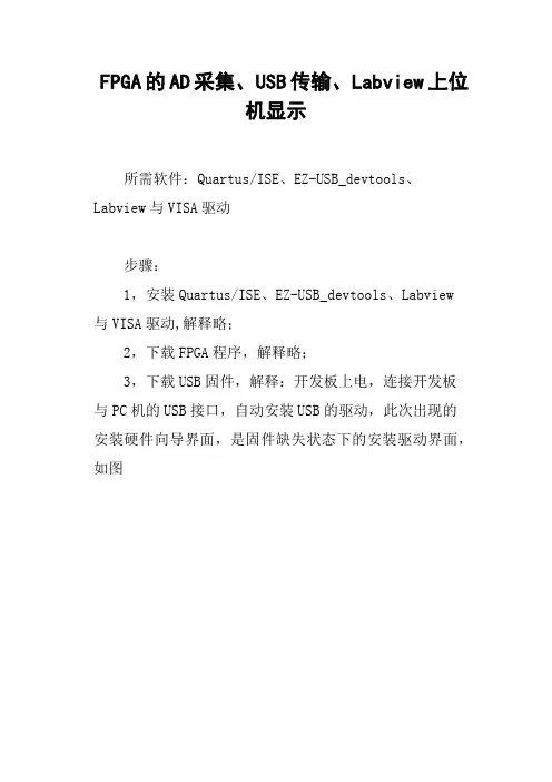
FPGA的AD采集、USB传输、Labview上位机显示所需软件:Quartus/ISE、EZ-USB_devtools、Labview与VISA驱动步骤:1,安装Quartus/ISE、EZ-USB_devtools、Labview与VISA驱动,解释略;2,下载FPGA程序,解释略;3,下载USB固件,解释:开发板上电,连接开发板与PC机的USB接口,自动安装USB的驱动,此次出现的安装硬件向导界面,是固件缺失状态下的安装驱动界面,如图打开Cypress->;USB->;EZ-USBControlPanel,Target选择FX2,点击Downlod,下载固件程序,即后缀为.hex的文件,如图调试阶段的固件为.hex文件,掉电后该固件数据丢失,因此一般设计USB芯片通过IIC总线外扩一片E2PROM存储器,可以通过Hex2Bix.exe软件把.hex文件转化成.iic文件,在产品阶段下载.iic固件程序,(Cypress公司USB2.0的内核为51单片机,USB3.0的内核为arm9,开发USB固件程序指的就是编写内核单片机或者arm的程序,对USB2.0可以用KeiluVision2进行开发,跟51单片机的开发类似。
);下载完成后,如图会重新出现安装硬件向导,此次出现的安装硬件向导界面,是固件存在状态下的安装驱动界面,如图4,Labview驱动,解释:打开NationalInstruments->;VISADriverWizard,如图选择USB,next,点击Refresh,在DeviceList栏找到相应的USB的VID&PID(VID与PID的信息存储在固件程序里,可以通过对固件程序的修改改变他们的值),选择VID&PID后,在右侧的ManufacturerName和ModelName栏会出现相应的USB信息,可以看到ModelName为使用的EZ-USBFX2,如图next,生成Labview的USB驱动为prefix,可以选择驱动存放位置,如图next,确定创建驱动,如图安装驱动,如图如果安装不成功,可以找到驱动存放的位置,手动安装,右键prefix.inf安装即可,如图如果仍不成功,重复Labview驱动这一步骤,Labview驱动这一块有时会出现问题;5,Labview应用程序,解释:打开NationalInstruments->;LabVIEW2011->;LabVIEW,打开应用程序,后面板如图前面板如图选择USB设备,刷新,找到USB设备,如图点击运行,如图采集到的直流信号,如图采集到的交流信号,如图采集到的图像信号,如图。
使用LabVIEW和FPGA来创建一个自动化的微控制器测试系统

使用LabVIEW和FPGA来创建一个自动化的微控制器测试系统对于之前的应用程序测试平台,我们使用公司内部开发的控制器板,但该板需要一套单独的兼容工具链来下载这些应用程序。
此外,我们还很难对这些工具链的用户界面进行导航,不得不使用额外的测试和测量设备。
有了虚拟仪器,我们可以使用同一套软件和模块化硬件执行以下测试:测试常见的协议(SPI, ASC, I2C) 测试PWM,ICU 测试模拟/数字转换器测试控制器区域网络(CAN) 测试时钟和门控测试多模块同时运行系统对于需要测试的应用来说,使用FPGA 的可重编程功能,它和LabVIEW 之间的自动化接口以及CAN 分析仪功能,我们可以很容易地开发我们的系统。
在整个框架上,我们节省了大量的时间和成本。
在此之前,对于微控制器的每个模块/外设,测试十至二十个案例我们需要花费四至五个小时。
使用我们所创建的基于NI 产品的系统,相同的一组测试执行时间在十到十五分钟内,而且测试质量显著地提高。
我们需要合适的测试平台应用程序以测试微控制器的不同外设。
比如,为了测试SPI 接口,我们需要建立SPI 主机或者从机作为测试平台。
我们使用LabVIEW FPGA VIs(CAN 接口的CAN VI)来创建每个测试平台。
框架内测试案例构造则是指各自的VI。
在框架中,我们可以创建一个LabVIEW 对象以获取VI 引用,对于每个测试案例的需求,都为用户配置了输入控件和显示控件。
执行自动化框架中的测试案例,需要调用特定的VI,配置该VI,最后运行它。
该框架无需用户参与就可以执行测试。
比如,测量PWM 信号的解决方案如下:VI 测量占空比和信号频率,然后将其保存到Excel 文件中。
另一种解决方案涉及从SPI 主机接收数据。
作为从机SPI 的VI 可以从主机测试设备(DUT)中接收数据。
SPI 从机工作在不同的波特率和变化的数据比特下。
用户可以配置VI,而其运行取决于测试设备(DUT)的主SPI 的配置。
labview fpga教程
labview fpga教程
LabVIEW FPGA教程是一种基于LabVIEW图形化编程语言的教程,主要用于FPGA设备编程的培训和学习。
FPGA(Field-Programmable Gate Array)是一种可编程逻辑器件,具有较高的并行计算能力和灵活性,广泛应用于数字信号处理、图像处理、嵌入式系统设计等领域。
LabVIEW FPGA教程主要包括以下方面的内容: 1. FPGA开发平台的介绍和操作:介绍FPGA的硬件架构、板卡配置、编程软件等基础知识,让学员
了解如何借助FPGA来解决各种复杂的工程问题。
2. LabVIEW FPGA编程基础:介绍基础的LabVIEW FPGA图形化编程语言和运行环境,涵盖数据类型、图表、函数、结构、模块化编程等方面的内容。
3. FPGA项目实战:让学员动手实现项目,将
所学的理论知识应用于实际工程中,例如控制器设计、图像处理、信号处理、通信接口等。
4. FPGA应用案例:介绍FPGA 在不同领域的应用案例,如医疗器械、卫星通信、人工智能等,让学员了解FPGA的广泛应用场景和未来的发展趋势。
通过LabVIEW FPGA教程的学习,学员能够掌握FPGA的基础。
深入了解LabVIEW FPGA
一旦您选择 NI RIO 设备上的 FPGA 作为目标对象,LabVIEW 将只显示 FPGA 可以实现的功能 (图 2), 更加方便您使用 LabVIEW 对 FPGA 进行编程。LabVIEW FPGA 模块函数面板包括典型的 LabVIEW 结 构和函数,如 While 循环,For 循环,条件结构,顺序结构以及 LabVIEW FPGA 针对数学、信号生成和 分析、线性和非线性控制、比较逻辑、数组和簇操作、并发、模拟和数字 I/O,以及定时等方面的专用 函数。您可以使用这些函数进行组合,定义逻辑功能,并将其嵌入到您的 NI RIO 设备当中。
深入了解 LabVIEW FPGA
NI 通过 LabVIEW FPGA 模块和可重复配置 I/O(RIO)硬件设备,为测量和控制系统中整合 FPGA 技术的 灵活性提供了直观且现成可用的解决方案。您可以使用 LabVIEW 图形化编程定义 FPGA 芯片上的逻辑 功能,您不需要任何的有关底层硬件描述语言(HDLs)的知识,如 VHDL 或是 Verilog,也不需要了解板 卡级硬件设计,就可以将 FPGA 芯片嵌入到 NI 可重复配置 I/O 系列硬件目标当中。另外,LabVIEW 还 可以让您轻松地集成图象采集/分析、运动控制,以及 CAN 和 RS232 等工业通信功能。
LabVIEW FPGA开发指导1-2-3
二进制补码表示 整数字长(iwl) 小数字长(fwl) 有限的量程 指定的 符号位 小数点位置 确定的分辨力 两头归一化,+/-1内计算,整数字长通常不变 参见GSDZone《聚星2010LabVIEW研讨会》
算法仿真
• 仿真方法
– 主机VI – 在主机运行FPGA程序 – FPGA VI拉到主机改编后运行
NI FPGA开发2:开始编程
• 算法仿真 • 模块构建
– – – – 采集-处理-输出框架 数字信号处理 和主机通信 处理速度优化
算法仿真步骤
• 数组运算 到 逐点运算 • 浮点数 到定点数
关于定点数
b31b30
32位字长(wl)
………… b18 17 b ………… b2b1b0
• • • • •
FREE
• 随LV FPGA模块附带 • NIFPGA2009\Xilinx\ISE\bin\nt\coregen.exe
DDS Filter
FFT
……
说明详尽、功能强大、资源利用充分
处理速度的优化:极品飞车
• 加快时钟
– 设置倍频时钟 – 选择 top-level clock
• FPGA资源换速度 • 流水线和延时换速度 • 使用单时钟周期循环
LabVIEW FPGA 1-2-3
邵晖 博士 聚星仪器有限公司
概要
• NI LabVIEW FPGA应用案例 • NI FPGA产品开发一二三
– 准备工作 – 编程 – 调试与测试
• FPGA开发四五六 • 总结
FPGA产品系列的优点
• • • • • • • • 逻辑可靠 反馈控制响应快 技术独特不容易破解 测量准确可靠 耐恶劣环境(宽温、抗振抗冲击、防爆) 接口模块皮实 (热插拔、隔离) 功耗低 (CompactRIO典型10-15W) 体积、重量不大
LabVIEW FPGA开发PWM接口基础应用教程
LabVIEW FPGA 开发PWM 接口基础应用教程
开发和测试汽车电子、航空电子设备及数字传感器的工程师和设计师们,经常需要测量和模拟设备所产生的脉冲宽度调制(Pulse Width ModulaTIon, PWM)信号。
LabVIEW FPGA 模块可以用来为测试测量系统创建PWM 接口。
与专用的PWM I/O 设备不同的是,LabVIEW FPGA 允许自定义应用程序的PWM 通道特性和行为,并且可以与其它的测量设备集成和同步。
1. 应用程序概述
LabVIEW FPGA 模块和可重配置的I/O 板卡可以用来实现各种自定义接口,其中包括:
- 用于其它测量设备的定时和触发功能
- 数字通信协议
- 开发快速原型或者硬件在环应用中的设备仿真
- AC 和DC 传感器仿真。
- 1、下载文档前请自行甄别文档内容的完整性,平台不提供额外的编辑、内容补充、找答案等附加服务。
- 2、"仅部分预览"的文档,不可在线预览部分如存在完整性等问题,可反馈申请退款(可完整预览的文档不适用该条件!)。
- 3、如文档侵犯您的权益,请联系客服反馈,我们会尽快为您处理(人工客服工作时间:9:00-18:30)。
[LabVIEW FPGA教程]将外部IP导入LabVIEW FPGA
概览
通过将第三方IP 集成到NI LabVIEW软件,您能使用许多的针对Xilinx现场可编程门整列
(Field-programmable gate arrays, FPGA)进行优化的算法,在实现高性能的同时提高代码重用度。
LabVIEW FPGA模块提供两种方法用来实现外部代码的导入:组件级IP(Component-Level Intellectual Property, CLIP)节点和IP集成节点。
本白皮书将讨论这两种方法。
目录
1. CLIP节点介绍
2. 在FPGA应用中使用CLIP
3. IP集成节点介绍
4. CLIP和IP集成节点的区别
5. 相关资源
1. CLIP节点介绍
CLIP节点是一种用于将已有的FPGA IP导入LabVIEW FPGA硬件的同时通过LabVIEW FPGA程序框图与它进行通讯的框架。
一旦导入成功,相对于LabVIEW FPGA,IP可以独立地、并行地运行。
IP既能以原始VHDL的形式也能以诸如电子设计交换格式(Electronic design interchange format, EDIF)网表等中间文件的形式存在。
这一功能要求使用者具有一定数字电路设计经验和VHDL的基本知识,因为所导入的IP 通常是一种底层的硬件描述语言(Hardware description language, HDL)。
对于不同的FPGA目标,其所支持的CLIP也不同。
请参考目标硬件的的定义文档获取关于CLIP支持的信息。
部分FPGA目标可支持以下一种或者两种类型的CLIP:
用户定义的CLIP—导入VHDL代码,直接与FPGA VI进行通讯。
套接字CLIP—导入VHDL代码,直接和不与LabVIEW FPGA模块关联的一个FPGA VI以及FPGA引脚进行通信。
一些FPGA目标在FPGA中定义了一个您可以插入套接字CLIP的固定式CLIP套接字。
图1.在由使用者定义的CLIP节点中导入VHDL代码可以与一个FPGA VI进行通讯;反之,一个套接字CLIP节点允许IP同时连接到FPGA VI和可用FPGA引脚。
获取最新的信息,请参考标题为使用VHDL代码作为组件级IP(FPGA模块)的LabVIEW FPGA模块帮助。
2. 在FPGA应用中使用CLIP
1. 创建或者获取IP。
2. 在FPGA目标属性中声明CLIP以及定义IP接口。
3. 将CLIP添加到项目中。
4. 在一个FPGA VI中使用CLIP。
创建或者获取IP
要将CLIP添加到一个FPGA目标中,您必须提供VHDL代码形式的IP以编译成FPGA对象。
您能使用以下方式提供VHDL代码::
o创建VHDL代码。
o通过其它的硬件描述语言(HDL)创建您自己的可兼容IP核心,例如通过Xilinx CORE Generator 利用Verilog进行创建。
o从Xilinx或合作伙伴那购买IP核心。
注意:在LabVIEW FPGA的CORE Generator IP选板中有超过50种Xilinx IP模块,无需使用CLIP或IP 集成节点导入IP模块您就能将其集成到您的LabVIEW FPGA VI的数据流中。
了解如何使用Xilinx CORE GeneratorIP选板提高IP的重用度。
在使用CLIP节点时,需要特别注意的是LabVIEW FPGA所支持的数据类型以及如何将它们转换为VHDL 数据类型。
如果您的IP使用的逻辑向量并不不是表一中所列的数据类型之一,您必须编写一个VHDL外层程序来对标准LabVIEW类型进行扩展、缩短或者分解,从而符合IP的数据宽度。
请参考LabVIEW FPGA模块帮助,获取更多关于您IP的注意事项,包括使用外部时钟、交叉时钟域、使用同步寄存器、执行异步重置,以及使用约束和层次条件。
1. 创建一个带有FPGA硬件新LabVIEW项目。
右键点击FPGA目标,并选择属性。
属性对话框有一段
标有“组件级IP(Component-Level IP)”的部分。
点击创建文件按钮创建XML文件。
图2. 点击“Create File”开始定义XML声明文档。
1. 点击Add Synthesis File…按钮,并浏览代表顶层组件IP(即simple_and.vhd )的VHDL文档.再
点击Next>
图3. 添加了您的IP的综合文件后,点击Next>。
2. 配置向导的余下部分用来安装XML声明文档。
本例中,点击Next>按钮默认安装向导的余下部分,验
证输入文件的语法,再点击剩下的Next>按钮。
图4. 配置向导中生成的XML声明文件必须为导入的IP模块而列出。
一旦您完成了CLIP配置向导,CLIP声明名称(在XML文档中已定义)将出现在文件的路径旁。
在本对话框中,您能够为需要导入的所有不同IP模块声明多个CLIP节点。
将一个CLIP项添加到一个LabVIEW项目中
在FPGA中声明CLIP实际上并没有将它添加到项目中去,因为你能够在同一个FPGA上完成一个CLIP 的多个实例。
在下一步中,你将创建一个先前已经被声明的simpleAND CLIP项的实例。
1. 右键点击FPGA目标,并选择New Component-Level IP。
在CLIP对话框中会出现选择所需的CLIP,
给这个实例一个唯一的标识名,以及通过“Clock”信号类型,选择时钟连接到CLIP中的任意线路。
在本例中,后面两个选项默认不选。
图5. 本对话框显示当你将一个CLIP的实例添加到项目中后,选择CLIP,定义一个名称,同时配置
时钟。
2. 一旦您点击本对话框中的OK按钮,本CLIP和出现在项目中的所有与之相关的输入和输出都被标有
该实例的名称。
图6. 添加CLIP后的项目后,显示IP的所有I/O节点。
在CLIP和一个FPGA VI之间传递数据
此时,你已经准备好在CLIP和FPGA VI间进行通讯。
你要做的只是从项目中将所需的I/O节点拖放到FPGA 框图中。
您的IP必须具有如何使用IP的文档。
比如,许多IP模块使用一些类型的握手线用于数据的输入和输出,它们通常被标记为“data valid ”或者“enable”。
使用LabVIEW的数据类型,在正确的时间发送正确的数值,即可运行IP。
您可将CLIP I/O放置在一个单周期定时循环(Single-cycle Timed Loop, SCTL)内部或者外部,但是请记住,在一个SCTL内部,你可能需要考虑时钟域交叉以及使用同步寄存器。
图7. 为了在LabVIEW FPGA中与CLIP进行通讯,将项目窗口中IP输入和输出拖放到FPGA VI的框图
中。
图8. 使用CLIP,整个的LabVIEW FPGA方框图与所导入的IP进行通讯。
3. IP集成节点介绍
注意:这个IP集成节点范例将导入附件中的demo_adder.vhd IP模块。
1. 创建一个带有FPGA目标的LabVIEW项目,同时在FPGA目标下添加一个新的VI
2. 在新建的VI的程序框图中,从编程选板中拖放一个IP Integration Node,保存FPGA VI,再双击节点
打开配置向导对话框。
图9. 双击IP集成节点,使用属性配置向导开始导入步骤。
1. 点击Add Synthesis File,在弹出的窗口中选择demo_adder.vhd文档。
2. 返回到配置向导对话框,两次点击Next>选择默认选项。
3. 在文件生成步骤,首先确认导入的VHDL文档的语法,然后通过点击如下所示的各个按钮生成支持文
件。
图10. 配置向导使帮助您在生成必须的LabVIEW支持文件之前检查您的VHDL IP的语法。
1. 一旦IP生成成功,在后续的三步中选择Next>保持默认选项。
2. 在配置向导的最后一步中,你能够为不同的终端选择数据类型。
对这一IP模块,默认的定点数据类型
即可满足要求。
点击Finish按钮完成生成。
3. IP集成节点现已配置成功,同时您可以将其集成进您的其它的LabVIEW FPGA应用中。
图11. IP集成节点及其集成的IP
4. CLIP和IP集成节点的区别
CLIP 和IP集成节点是将外部IP导入LabVIEW FPGA的两种方式,你必须根据以下的标准在二者之间进行选择。
CLIP节点能够与您在LabVIEW FPGA中开发的IP 独立地并行运行。
此外,CLIP能够直接与FPGA时钟和I/O引脚进行联接。
与此相反,IP集成节点则被植入LabVIEW FPGA程序框图中,并按照LabVIEW VI数据流所定义的方式执行。
作为LabVIEW 数据流的一部分,使用周期精准的仿真工具,IP 集成节点使您可以验证整体的应用行为和时序。
表格2. 概述了两种节点之间的区别。
5. 相关资源
按需提供的培训:使用CLIP)将外部代码导入LabVIEW FPGA(需要SSP)
LabVIEW官方主页。