TC74LVX573FT(EL),TC74LVX573FW,TC74LVX573FW(ELP), 规格书,Datasheet 资料
74HC573数据手册
2. Features and benefits
Input levels: For 74HC573: CMOS level For 74HCT573: TTL level
Inputs and outputs on opposite sides of package allowing easy interface with microprocessors
data input
10
ground (0 V)
11
latch enable input (active HIGH)
19, 18, 17, 16, 15, 14, 13, 12 3-state latch output
20
supply voltage
74HC_HCT573
Product data sheet
Q0 19 Q1 18 Q2 17 3-STATE Q3 16 OUTPUTS Q4 15 Q5 14 Q6 13 Q7 12
mna809
74HC_HCT573
Product data sheet
All information provided in this document is subject to legal disclaimers.
5.2 Pin description
Table 2. Symbol OE D[0:7] GND LE Q[0:7] VCC
Pin description
Pin
Description
1
3-state output enable input (active LOW)
2, 3, 4, 5, 6, 7, 8, 9
HBM JESD22-A114F exceeds 2 000 V MM JESD22-A115-A exceeds 200 V Specified from 40 C to +85 C and from 40 C to +125 C
74LVC1G3157二路模拟多路复用 多路解复用数据手册说明书
74LVC1G31572-channel analog multiplexer/demultiplexerRev. 7 — 14 February 2017Product data sheet1General descriptionThe 74LVC1G3157 provides one analog multiplexer/demultiplexer with one digital selectinput (S), two independent inputs/outputs (Y0, Y1) and a common input/output (Z).Schmitt trigger action at the select input makes the circuit tolerant of slower input rise andfall times across the entire V CC range from 1.65 V to 5.5 V.2Features and benefits•Wide supply voltage range from 1.65 V to 5.5 V•Very low ON resistance:–7.5 Ω (typical) at V CC = 2.7 V–6.5 Ω (typical) at V CC = 3.3 V–6 Ω (typical) at V CC = 5 V•Switch current capability of 32 mA•Break-before-make switching•High noise immunity•CMOS low power consumption•TTL interface compatibility at 3.3 V•Latch-up performance meets requirements of JESD 78 Class I•ESD protection:–HBM JESD22-A114F exceeds 2000 V–MM JESD22-A115-A exceeds 200 V•Control input accepts voltages up to 5.5 V•Multiple package options•Specified from -40 °C to +85 °C and from -40 °C to +125 °C2-channel analog multiplexer/demultiplexer 3Ordering information4Marking[1]The pin 1 indicator is located on the lower left corner of the device, below the marking code.2-channel analog multiplexer/demultiplexer5Functional diagram6Pinning information6.1Pinning74LVC1G3157Y1S GND Y0Z001aac3561236V CC 54Figure 3. Pin configuration SOT363 and SOT45774LVC1G3157ZV CCSY0GND Y1001aac357342516T ransparent top viewFigure 4. Pin configuration SOT88674LVC1G3157GND 001aaf546Y1Y0V CC S ZT ransparent top view231546Figure 5. Pin configuration SOT891, SOT1115 and SOT1202aaa-022365Transparent top view74LVC1G315734Y0Z16Y1S 2GND5V CC Figure 6. Pin configuration SOT12552-channel analog multiplexer/demultiplexer6.2Pin description7Functional description[1][1]H = HIGH voltage level;L = LOW voltage level.8Limiting valuesTable 5. Limiting valuesIn accordance with the Absolute Maximum Rating System (IEC 60134). Voltages are referenced to GND (ground = 0 V).[1]The minimum input voltage rating may be exceeded if the input current rating is observed.[2]The minimum and maximum switch voltage ratings may be exceeded if the switch clamping current rating is observed.[3]For SC-88 and SC-74 packages: above 87.5 °C the value of P tot derates linearly with 4.0 mW/K.For XSON6 and X2SON6 packages: above 118 °C the value of P tot derates linearly with 7.8 mW/K.2-channel analog multiplexer/demultiplexer 9Recommended operating conditions[1]To avoid sinking GND current from terminal Z when switch current flows in terminal Yn, the voltage drop across the bidirectional switch must not exceed0.4 V. If the switch current flows into terminal Z, no GND current will flow from terminal Yn. In this case, there is no limit for the voltage drop across theswitch.[2]Applies to control signal levels.10Static characteristicsTable 7. Static characteristicsAt recommended operating conditions; voltages are referenced to GND (ground 0 V).2-channel analog multiplexer/demultiplexer[1]Typical values are measured at T amb = 25 °C.[2]These typical values are measured at V CC = 3.3 V10.1Test circuits2-channel analog multiplexer/demultiplexer10.2ON resistanceTable 8. ON resistanceAt recommended operating conditions; voltages are referenced to GND (ground 0 V); for graphs see Figure 10 to Figure 15.[1]Typical values are measured at T amb = 25 °C and nominal V CC.[2]Flatness is defined as the difference between the maximum and minimum value of ON resistance measured at identical V CC and temperature.2-channel analog multiplexer/demultiplexer 10.3ON resistance test circuit and graphs2-channel analog multiplexer/demultiplexer2-channel analog multiplexer/demultiplexer 11Dynamic characteristicsTable 9. Dynamic characteristicsAt recommended operating conditions; voltages are referenced to GND (ground = 0 V); for test circuit see Figure 19.[1]Typical values are measured at T amb = 25 °C and nominal V CC.[2]t pd is the same as t PLH and t PHL.[3]Propagation delay is the calculated RC time constant of the typical ON resistance of the switch and the specified capacitance when driven by an idealvoltage source (zero output impedance).[4]t en is the same as t PZH and t PZL.[5]t dis is the same as t PLZ and t PHZ.[6]Break-before-make specified by design.2-channel analog multiplexer/demultiplexer 11.1Waveforms and test circuits2-channel analog multiplexer/demultiplexer2-channel analog multiplexer/demultiplexer11.2Additional dynamic characteristicsTable 12. Additional dynamic characteristicsAt recommended operating conditions; voltages are referenced to GND (ground = 0 V); T= 25 °C.2-channel analog multiplexer/demultiplexer 11.3Test circuits2-channel analog multiplexer/demultiplexer2-channel analog multiplexer/demultiplexer 12Package outline2-channel analog multiplexer/demultiplexer2-channel analog multiplexer/demultiplexer2-channel analog multiplexer/demultiplexer2-channel analog multiplexer/demultiplexer2-channel analog multiplexer/demultiplexer2-channel analog multiplexer/demultiplexer2-channel analog multiplexer/demultiplexer 13Abbreviations14Revision history2-channel analog multiplexer/demultiplexer 15Legal information15.1 Data sheet status[1]Please consult the most recently issued document before initiating or completing a design.[2]The term 'short data sheet' is explained in section "Definitions".[3]The product status of device(s) described in this document may have changed since this document was published and may differ in case of multipledevices. The latest product status information is available on the Internet at URL .15.2 DefinitionsDraft — The document is a draft version only. The content is still under internal review and subject to formal approval, which may result in modifications or additions. Nexperia does not give any representations or warranties as to the accuracy or completeness of information included herein and shall have no liability for the consequences of use of such information.Short data sheet — A short data sheet is an extract from a full data sheet with the same product type number(s) and title. A short data sheet is intended for quick reference only and should not be relied upon to contain detailed and full information. For detailed and full information see the relevant full data sheet, which is available on request via the local Nexperia sales office. In case of any inconsistency or conflict with the short data sheet, the full data sheet shall prevail.Product specification — The information and data provided in a Product data sheet shall define the specification of the product as agreed between Nexperia and its customer, unless Nexperia and customer have explicitly agreed otherwise in writing. In no event however, shall an agreement be valid in which the Nexperia product is deemed to offer functions and qualities beyond those described in the Product data sheet.15.3 DisclaimersLimited warranty and liability — Information in this document is believed to be accurate and reliable. However, Nexperia does not give any representations or warranties, expressed or implied, as to the accuracyor completeness of such information and shall have no liability for the consequences of use of such information. Nexperia takes no responsibility for the content in this document if provided by an information source outside of Nexperia. In no event shall Nexperia be liable for any indirect, incidental, punitive, special or consequential damages (including - without limitation -lost profits, lost savings, business interruption, costs related to the removal or replacement of any products or rework charges) whether or not such damages are based on tort (including negligence), warranty, breach of contract or any other legal theory. Notwithstanding any damages that customer might incur for any reason whatsoever, Nexperia's aggregate and cumulative liability towards customer for the products described herein shall be limited in accordance with the Terms and conditions of commercial sale of Nexperia.Right to make changes — Nexperia reserves the right to make changesto information published in this document, including without limitation specifications and product descriptions, at any time and without notice. This document supersedes and replaces all information supplied prior to the publication hereof.Suitability for use — Nexperia products are not designed, authorized or warranted to be suitable for use in life support, life-critical or safety-critical systems or equipment, nor in applications where failure or malfunctionof an Nexperia product can reasonably be expected to result in personal injury, death or severe property or environmental damage. Nexperia and its suppliers accept no liability for inclusion and/or use of Nexperia products in such equipment or applications and therefore such inclusion and/or use is at the customer’s own risk.Applications — Applications that are described herein for any of these products are for illustrative purposes only. Nexperia makes no representation or warranty that such applications will be suitable for the specified use without further testing or modification. Customers are responsible for the design and operation of their applications and products using Nexperia products, and Nexperia accepts no liability for any assistance with applications or customer product design. It is customer’s sole responsibility to determine whether the Nexperia product is suitable and fit for the customer’s applications and products planned, as well as for the planned application and use of customer’s third party customer(s). Customers should provide appropriate design and operating safeguards to minimize the risks associated with their applications and products. Nexperia does not accept any liability related to any default, damage, costs or problem which is based on any weakness or default in the customer’s applications or products, or the application or use by customer’s third party customer(s). Customer is responsible for doing all necessary testing for the customer’s applications and products using Nexperia products in order to avoid a default of the applications and the products or of the application or use by customer’s third party customer(s). Nexperia does not accept any liability in this respect.Limiting values — Stress above one or more limiting values (as defined in the Absolute Maximum Ratings System of IEC 60134) will cause permanent damage to the device. Limiting values are stress ratings only and (proper) operation of the device at these or any other conditions above thosegiven in the Recommended operating conditions section (if present) or the Characteristics sections of this document is not warranted. Constant or repeated exposure to limiting values will permanently and irreversibly affect the quality and reliability of the device.Terms and conditions of commercial sale — Nexperia products aresold subject to the general terms and conditions of commercial sale, as published at /profile/terms, unless otherwise agreed in a valid written individual agreement. In case an individual agreement is concluded only the terms and conditions of the respective agreement shall apply. Nexperia hereby expressly objects to applying the customer’s general terms and conditions with regard to the purchase of Nexperia products by customer.No offer to sell or license — Nothing in this document may be interpreted or construed as an offer to sell products that is open for acceptance orthe grant, conveyance or implication of any license under any copyrights, patents or other industrial or intellectual property rights.Export control — This document as well as the item(s) described herein may be subject to export control regulations. Export might require a prior authorization from competent authorities.2-channel analog multiplexer/demultiplexerNon-automotive qualified products — Unless this data sheet expressly states that this specific Nexperia product is automotive qualified, the product is not suitable for automotive use. It is neither qualified nor tested in accordance with automotive testing or application requirements. Nexperia accepts no liability for inclusion and/or use of non-automotive qualified products in automotive equipment or applications. In the event that customer uses the product for design-in and use in automotive applications to automotive specifications and standards, customer (a) shall use the product without Nexperia's warranty of the product for such automotive applications, use and specifications, and (b) whenever customer uses the product for automotive applications beyond Nexperia's specifications such use shall be solely at customer’s own risk, and (c) customer fully indemnifies Nexperia for any liability, damages or failed product claims resulting from customer design and use of the product for automotive applications beyond Nexperia's standard warranty and Nexperia's product specifications.Translations — A non-English (translated) version of a document is for reference only. The English version shall prevail in case of any discrepancy between the translated and English versions.15.4 TrademarksNotice: All referenced brands, product names, service names and trademarks are the property of their respective owners.2-channel analog multiplexer/demultiplexerPlease be aware that important notices concerning this document and the product(s)described herein, have been included in section 'Legal information'.Contents1General description ............................................12Features and benefits .........................................13Ordering information ..........................................24Marking .................................................................25Functional diagram .............................................36Pinning information ............................................36.1Pinning ...............................................................36.2Pin description ...................................................47Functional description ........................................48Limiting values ....................................................49Recommended operating conditions ................510Static characteristics ..........................................510.1Test circuits .......................................................610.2ON resistance ....................................................710.3ON resistance test circuit and graphs ................811Dynamic characteristics ...................................1011.1Waveforms and test circuits ............................1111.2Additional dynamic characteristics ...................1311.3Test circuits .....................................................1412Package outline .................................................1613Abbreviations ....................................................2314Revision history (2315)Legal information (24)。
74AHC573 74AHCT573 CMOS 高速透明储存器说明书
74AHC573; 74AHCT573Octal D-type transparant latch; 3-stateRev. 7 — 8 November 2011Product data sheet1. General descriptionThe 74AHC573; 74AHCT573 is a high-speed Si-gate CMOS device and is pin compatiblewith Low-power Schottky TTL (LSTTL). It is specified in compliance with JEDEC standardNo.7A.The 74AHC573; 74AHCT573 consists of eight D-type transparent latches featuringseparate D-type inputs for each latch and 3-state true outputs for bus orientedapplications. A latch enable input (LE) and an output enable input (OE) are common to alllatches.When pin LE is HIGH, data at the Dn inputs enters the latches. In this condition thelatches are transparent, i.e. a latch output will change state each time its correspondingDn input changes. When pin LE is LOW, the latches store the information that is presentat the Dn inputs, after a set-up time preceding the HIGH-to-LOW transition of LE.When pin OE is LOW, the contents of the 8latches are available at the outputs. Whenpin OE is HIGH, the outputs go to the high-impedance OFF-state. Operation of the OEinput does not affect the state of the latches.The 74AHC573; 74AHCT573 is functionally identical to the 74AHC373; 74AHCT373, buthas a different pin arrangement.2. Features and benefits⏹Balanced propagation delays⏹All inputs have a Schmitt trigger action⏹Common 3-state output enable input⏹Functionally identical to the 74AHC373; 74AHCT373⏹Inputs accept voltages higher than V CC⏹Input levels:◆For 74AHC573: CMOS input level◆For 74AHCT573: TTL input level⏹ESD protection:◆HBM EIA/JESD22-A114E exceeds 2000V◆MM EIA/JESD22-A115-A exceeds 200V◆CDM EIA/JESD22-C101C exceeds 1000V⏹Multiple package options⏹Specified from -40︒C to +85︒C and from -40︒C to +125︒C3. Ordering information4. Functional diagramTable 1.Ordering informationType numberPackageTemperature rangeNameDescriptionVersion74AHC57374AHC573D -40︒C to +125︒C SO20plastic small outline package; 20leads;body width 7.5mmSOT163-174AHC573PW -40︒C to +125︒C TSSOP20plastic thin shrink small outline package; 20leads; body width 4.4mmSOT360-174AHC573BQ-40︒C to +125︒CDHVQFN20plastic dual in-line compatible thermal enhanced very thin quad flat package no leads; 20 terminals; body 2.5⨯4.5⨯0.85mmSOT764-174AHCT57374AHCT573D -40︒C to +125︒C SO20plastic small outline package; 20leads; body width 7.5mmSOT163-174AHCT573PW -40︒C to +125︒C TSSOP20plastic thin shrink small outline package; 20leads; body width 4.4mmSOT360-174AHCT573BQ-40︒C to +125︒CDHVQFN20plastic dual in-line compatible thermal enhanced very thin quad flat package no leads; 20 terminals; body 2.5⨯4.5⨯0.85mmSOT764-15. Pinning information5.1Pinning5.2Pin descriptionTable 2.Pin descriptionSymbol Pin DescriptionOE1output enable input (active LOW) D0 to D72, 3, 4, 5, 6, 7, 8, 9data inputGND10ground (0V)LE11latch enable (active HIGH)Q0 to Q719, 18, 17, 16, 15, 14, 13, 12data outputV CC20supply voltage6. Functional description[1]H =HIGH voltage level;h =HIGH voltage level one set-up time prior to the HIGH-to-LOW LE transition;L =LOW voltage level;l =LOW voltage level one set-up time prior to the HIGH-to-LOW LE transition;Z =high-impedance OFF-state.7. Limiting values[1]The input and output voltage ratings may be exceeded if the input and output current ratings are observed.[2]For SO20 packages: above 70︒C the value of P tot derates linearly at 8mW/K.For TSSOP20 packages: above 60︒C the value of P tot derates linearly at 5.5mW/K.For DHVQFN20 packages: above 60︒C the value of P tot derates linearly with 4.5mW/K.Table 3.Function table [1]Operating modeInput Internal latch Output OE LE Dn Qn Enable and read register (transparent mode)L H L L L H H H Latch and read registerL L l L L h H H Latch register and disable outputsHLl L Z hHZTable 4.Limiting valuesIn accordance with the Absolute Maximum Rating System (IEC 60134).Voltages are referenced to GND (ground = 0V).Symbol Parameter Conditions Min Max Unit V CC supply voltage -0.5+7.0V V I input voltage-0.5+7.0V I IK input clamping current V I < -0.5V[1]-20-mA I OK output clamping current V O <-0.5V or V O >V CC +0.5V [1]-20+20mA I O output current V O = -0.5V to (V CC +0.5V)-25+25mA I CC supply current -+75mA I GND ground current -75-mA T stg storage temperature -65+150︒C P tottotal power dissipationT amb = -40 ︒C to +125︒C[2]-500mW8. Recommended operating conditions9. Static characteristicsTable 5.Operating conditions Symbol ParameterConditionsMinTypMaxUnit74AHC573V CC supply voltage 2.0 5.0 5.5V V I input voltage 0- 5.5V V O output voltage 0-V CC V T amb ambient temperature-40+25+125︒C ∆t/∆V input transition rise and fall rateV CC = 3.0 V to 3.6 V --100ns/V V CC = 4.5 V to 5.5 V--20ns/V74AHCT573V CC supply voltage 4.5 5.0 5.5V V I input voltage 0- 5.5V V O output voltage 0-V CC V T amb ambient temperature-40+25+125︒C ∆t/∆Vinput transition rise and fall rateV CC = 4.5 V to 5.5 V--20ns/VTable 6.Static characteristicsAt recommended operating conditions; voltages are referenced to GND (ground = 0V).Symbol Parameter Conditions25 ︒C -40︒C to +85 ︒C -40︒C to +125 ︒C UnitMin Typ Max Min Max Min Typ Max 74AHC573V IHHIGH-level input voltageV CC = 2.0 V 1.5-- 1.5- 1.5--V V CC = 3.0 V 2.1-- 2.1- 2.1--V V CC = 5.5 V3.85-- 3.85- 3.85--V V ILLOW-level input voltageV CC = 2.0 V --0.5-0.5--0.5V V CC = 3.0 V --0.9-0.9--0.9V V CC = 5.5 V-- 1.65- 1.65-- 1.65V V OHHIGH-level output voltage V I = V IH or V IL I O = -50μA; V CC =2.0 V1.92.0- 1.9- 1.9--V I O = -50μA; V CC =3.0 V 2.9 3.0- 2.9- 2.9--V I O = -50μA; V CC =4.5 V 4.4 4.5- 4.4- 4.4--V I O = -4.0mA; V CC =3.0 V 2.58-- 2.48- 2.40--V I O = -8.0mA; V CC =4.5 V3.94-- 3.80- 3.70--V V OLLOW-level output voltage V I = V IH or V IL I O = 50μA; V CC =2.0 V-00.1-0.1--0.1V I O = 50μA; V CC =3.0 V -00.1-0.1--0.1V I O = 50μA; V CC =4.5 V -00.1-0.1--0.1V I O = 4.0mA; V CC =3.0 V --0.36-0.44--0.55V I O = 8.0mA; V CC =4.5 V--0.36-0.44--0.55VI OZ OFF-stateoutput current V I=V IH or V IL;V O=V CC or GND;V CC=5.5V--±0.25-±2.5--±10.0μAI I input leakagecurrent V I=V CC or GND;V CC=0V to5.5V--0.1- 1.0-- 2.0μAI CC supply current V I=V CC or GND;I O=0A;V CC=5.5V-- 4.0-40--80μAC I inputcapacitanceV I=V CC or GND-310-10--10pFC O outputcapacitance-4-----10pF 74AHCT573V IH HIGH-levelinput voltageV CC = 4.5 V to 5.5 V 2.0-- 2.0- 2.0--VV IL LOW-levelinput voltageV CC = 4.5 V to 5.5 V--0.8-0.8--0.8VV OH HIGH-leveloutput voltage V I= V IH or V IL; V CC=4.5 VI O= -50μA 4.4 4.5- 4.4- 4.4--V I O= -8.0mA 3.94-- 3.80- 3.70--VV OL LOW-leveloutput voltage V I= V IH or V IL; V CC=4.5 VI O= 50μA-00.1-0.1--0.1V I O= 8.0mA--0.36-0.44--0.55VI OZ OFF-stateoutput current V I=V IH or V IL;V O=V CC or GND per inputpin; other inputs at V CC orGND; I O=0 A--±0.25-±2.5--±10.0μAI I input leakagecurrent V I=5.5 V or GND;V CC=0V to5.5V--0.1- 1.0-- 2.0μAI CC supply current V I=V CC or GND; I O = 0 A;V CC=5.5V-- 4.0-40--80μA∆I CC additionalsupply current per input pin;V I=V CC-2.1V; I O=0 A;other pins at V CC or GND;V CC=4.5V to5.5V-- 1.35- 1.5-- 1.5mAC I inputcapacitanceV I=V CC or GND-310-10--10pFC O outputcapacitance -4-----10pFTable 6.Static characteristics …continuedAt recommended operating conditions; voltages are referenced to GND (ground = 0V).Symbol Parameter Conditions25 ︒C-40︒C to+85 ︒C-40︒C to+125 ︒C UnitMin Typ Max Min Max Min Typ Max10. Dynamic characteristicsTable 7.Dynamic characteristicsVoltages are referenced to GND (ground = 0 V); for test circuit see Figure11.Symbol Parameter Conditions25 ︒C-40︒C to+85 ︒C-40︒C to+125 ︒C UnitMin Typ[1]Max Min Max Min Max74AHC573t pd propagationdelay Dn to Qn; see Figure7[2]V CC = 3.0 V to 3.6 VC L=15pF- 5.511.0 1.013.0 1.014.0nsC L=50pF-7.814.5 1.016.5 1.018.5ns V CC = 4.5 V to 5.5 VC L=15pF- 3.9 6.8 1.08.0 1.08.5nsC L=50pF- 5.58.8 1.010.0 1.011.0ns LE to Qn; see Figure8[2]V CC = 3.0 V to 3.6 VC L=15pF- 5.811.9 1.014.0 1.015.0nsC L=50pF-8.315.4 1.017.5 1.019.5ns V CC = 4.5 V to 5.5 VC L=15pF- 4.27.7 1.09.0 1.010.0nsC L=50pF- 5.99.7 1.011.0 1.012.5nst en enable time OE to Qn; see Figure9[3]V CC = 3.0 V to 3.6 VC L=15pF- 5.811.5 1.013.5 1.014.5nsC L=50pF-8.315.0 1.017.0 1.019.0nsV CC = 4.5 V to 5.5 VC L=15pF- 4.47.7 1.09.0 1.010.0nsC L=50pF- 6.39.7 1.011.0 1.012.5ns t dis disable time OE to Qn; see Figure9[4]V CC = 3.0 V to 3.6 VC L=15pF- 6.811.0 1.013.0 1.014.0nsC L=50pF-9.714.5 1.016.5 1.018.5nsV CC = 4.5 V to 5.5 VC L=15pF- 4.67.7 1.09.0 1.010.0nsC L=50pF-7.49.7 1.011.0 1.012.5ns t W pulse width LE HIGH; see Figure8V CC=3.0 V to 3.6 V 5.0-- 5.0- 5.0-nsV CC=4.5 V to 5.5 V 5.0-- 5.0- 5.0-ns t su set-up time Dn to LE; see Figure10V CC=3.0 V to 3.6 V 3.5-- 3.5- 3.5-nsV CC=4.5 V to 5.5 V 3.5-- 3.5- 3.5-ns[1]Typical values are measured at nominal supply voltage (V CC = 3.3V and V CC = 5.0V).[2]t pd is the same as t PHL and t PLH .[3]t en is the same as t PZH and t PZL .[4]t dis is the same as t PHZ and t PLZ .[5]C PD is used to determine the dynamic power dissipation (P D in μW).P D =C PD ⨯V CC 2⨯f i ⨯N +∑(C L ⨯V CC 2⨯f o )where:f i = input frequency in MHz;f o =output frequency in MHz;C L =output load capacitance in pF;V CC =supply voltage in V;N =number of inputs switching;∑(C L ⨯V CC 2⨯f o )=sum of the outputs.t hhold timeDn to LE; see Figure 10V CC =3.0 V to 3.6 V 1.5-- 1.5- 1.5-ns V CC =4.5 V to 5.5 V1.5-- 1.5- 1.5-ns C PDpower dissipation capacitancef i = 1 MHz;V I =GND to V CC[5]-12-----pF74AHCT573; V CC = 4.5 V to 5.5 V t pdpropagation delay Dn to Qn; see Figure 7[2]C L =15pF- 3.5 5.51 6.517.0ns C L =50pF- 4.97.518.519.5ns LE to Qn; see Figure 8[2]C L =15pF - 3.9 6.017.017.5ns C L =50pF- 5.58.519.5111.0ns t enenable timeOE to Qn; see Figure 9[3]C L =15pF - 4.1 6.517.518.5ns C L =50pF- 5.98.5110.0111.0ns t disdisable time OE to Qn; see Figure 9[4]C L =15pF - 4.5 6.517.518.5ns C L =50pF- 6.49.0110.0111.5ns t W pulse width LE HIGH; see Figure 8 5.0-- 5.0- 5.0-ns t su set-up time Dn to LE; see Figure 10 3.5-- 3.5- 3.5-ns t h hold time Dn to LE; see Figure 10 1.5-- 1.5- 1.5-ns C PDpower dissipation capacitancef i = 1 MHz;V I =GND to V CC[5]-18-----pFTable 7.Dynamic characteristics …continuedVoltages are referenced to GND (ground = 0 V); for test circuit see Figure 11.Symbol Parameter Conditions25 ︒C -40︒C to +85 ︒C -40︒C to +125 ︒C Unit MinTyp [1]Max Min Max Min Max11. WaveformsTable 8.Measurement pointsType Input OutputV M V M V X V Y74AHC5730.5⨯V CC0.5⨯V CC V OL + 0.3 V V OH- 0.3 V 74AHCT573 1.5 V0.5⨯V CC V OL + 0.3 V V OH- 0.3 VTable 9.Test dataType Input Load S1 positionV I t r, t f C L R L t PHL, t PLH t PZH, t PHZ t PZL, t PLZ 74AHC573V CC≤3.0ns15pF, 50pF1kΩopen GND V CC74AHCT573 3.0V≤3.0ns15pF, 50pF1kΩopen GND V CC12. Package outlineSO20: plastic small outline package; 20 leads; body width 7.5 mm SOT163-1Fig 12.Package outline SOT163-1 (SO20)TSSOP20: plastic thin shrink small outline package; 20 leads; body width 4.4 mm SOT360-1Fig 13.Package outline SOT360-1 (TSSOP20)Fig 14.Package outline SOT764-1 (DHVQFN20)SOT764-1DHVQFN20: plastic dual in-line compatible thermal enhanced very thin quad flat package; no leads;20 terminals; body 2.5 x 4.5 x 0.85 mm13. AbbreviationsTable 10.AbbreviationsAcronym DescriptionCDM Charged Device ModelCMOS Complementary Metal-Oxide SemiconductorESD ElectroStatic DischargeHBM Human Body ModelMM Machine ModelTTL Transistor-Transistor Logic14. Revision historyTable 11.Revision historyDocument ID Release date Data sheet status Change notice Supersedes74AHC_AHCT573 v.720111108Product data sheet-74AHC_AHCT573 v.6 Modifications:•Legal pages updated.74AHC_AHCT573 v.620101125Product data sheet-74AHC_AHCT573 v.5 74AHC_AHCT573 v.520100325Product data sheet-74AHC_AHCT573 v.4 74AHC_AHCT573 v.420100303Product data sheet-74AHC_AHCT573 v.3 74AHC_AHCT573 v.320080424Product data sheet-74AHC_AHCT573 v.2 74AHC_AHCT573 v.220031208Product specification-74AHC_AHCT573 v.1 74AHC_AHCT573 v.119990927Product specification--15. Legal information15.1 Data sheet status[1]Please consult the most recently issued document before initiating or completing a design.[2]The term ‘short data sheet’ is explained in section “Definitions”.[3]The product status of device(s) described in this document may have changed since this document was published and may differ in case of multiple devices. The latest product statusinformation is available on the Internet at URL .15.2 DefinitionsDraft — The document is a draft version only. The content is still under internal review and subject to formal approval, which may result in modifications or additions. Nexperia does not give anyrepresentations or warranties as to the accuracy or completeness of information included herein and shall have no liability for the consequences of use of such information.Short data sheet — A short data sheet is an extract from a full data sheet with the same product type number(s) and title. A short data sheet is intended for quick reference only and should not be relied upon to contain detailed and full information. For detailed and full information see the relevant full data sheet, which is available on request via the local Nexperia salesoffice. In case of any inconsistency or conflict with the short data sheet, the full data sheet shall prevail.Product specification — The information and data provided in a Product data sheet shall define the specification of the product as agreed between Nexperia and its customer, unless Nexperia andcustomer have explicitly agreed otherwise in writing. In no event however, shall an agreement be valid in which the Nexperia product isdeemed to offer functions and qualities beyond those described in the Product data sheet.15.3 DisclaimersLimited warranty and liability — Information in this document is believed to be accurate and reliable. However, Nexperia does not give any representations or warranties, expressed or implied, as to the accuracy or completeness of such information and shall have no liability for the consequences of use of such information.In no event shall Nexperia be liable for any indirect, incidental,punitive, special or consequential damages (including - without limitation - lost profits, lost savings, business interruption, costs related to the removal or replacement of any products or rework charges) whether or not such damages are based on tort (including negligence), warranty, breach of contract or any other legal theory.Notwithstanding any damages that customer might incur for any reason whatsoever, Nexperia’s aggregate and cumulative liability towards customer for the products described herein shall be limited in accordance with the Terms and conditions of commercial sale of Nexperia.Right to make changes — Nexperia reserves the right to makechanges to information published in this document, including without limitation specifications and product descriptions, at any time and without notice. This document supersedes and replaces all information supplied prior to the publication hereof.Suitability for use — Nexperia products are not designed,authorized or warranted to be suitable for use in life support, life-critical or safety-critical systems or equipment, nor in applications where failure or malfunction of a Nexperia product can reasonably be expectedto result in personal injury, death or severe property or environmental damage. Nexperia accepts no liability for inclusion and/or use ofNexperia products in such equipment or applications andtherefore such inclusion and/or use is at the customer’s own risk. Applications — Applications that are described herein for any of these products are for illustrative purposes only. Nexperia makes no representation or warranty that such applications will be suitable for the specified use without further testing or modification.Customers are responsible for the design and operation of their applications and products using Nexperia products, and Nexperiaaccepts no liability for any assistance with applications or customer product design. It is customer’s sole responsibility to determine whether the Nexperia product is suitable and fit for the customer’s applications andproducts planned, as well as for the planned application and use of customer’s third party customer(s). Customers should provide appropriate design and operating safeguards to minimize the risks associated with their applications and products.Nexperia does not accept any liability related to any default,damage, costs or problem which is based on any weakness or default in the customer’s applications or products, or the application or use by customer’s third party customer(s). Customer is responsible for doing all necessary testing for the customer’s applications and products using Nexperia products in order to avoid a default of the applications andthe products or of the application or use by customer’s third partycustomer(s). Nexperia does not accept any liability in this respect.Limiting values — Stress above one or more limiting values (as defined in the Absolute Maximum Ratings System of IEC60134) will cause permanent damage to the device. Limiting values are stress ratings only and (proper) operation of the device at these or any other conditions above those given in the Recommended operating conditions section (if present) or the Characteristics sections of this document is not warranted. Constant or repeated exposure to limiting values will permanently and irreversibly affect the quality and reliability of the device.Terms and conditions of commercial sale — Nexperiaproducts are sold subject to the general terms and conditions of commercial sale, as published at /profile/terms, unless otherwise agreed in a valid written individual agreement. In case an individual agreement is concluded only the terms and conditions of the respective agreement shall apply. Nexperia hereby expressly objects toapplying the customer’s general terms and conditions with regard to the purchase of Nexperia products by customer.No offer to sell or license — Nothing in this document may be interpreted or construed as an offer to sell products that is open for acceptance or the grant, conveyance or implication of any license under any copyrights, patents or other industrial or intellectual property rights.Export control — This document as well as the item(s) described herein may be subject to export control regulations. Export might require a prior authorization from competent authorities.Document status[1][2]Product status[3]DefinitionObjective [short] data sheet Development This document contains data from the objective specification for product development. Preliminary [short] data sheet Qualification This document contains data from the preliminary specification.Product [short] data sheet Production This document contains the product specification.Non-automotive qualified products — Unless this data sheet expressly states that this specific Nexperia product is automotive qualified,the product is not suitable for automotive use. It is neither qualified nor tested in accordance with automotive testing or application requirements. Nexperia accepts no liability for inclusion and/or use ofnon-automotive qualified products in automotive equipment or applications. In the event that customer uses the product for design-in and use in automotive applications to automotive specifications and standards, customer (a) shall use the product without Nexperia’s warranty of theproduct for such automotive applications, use and specifications, and (b) whenever customer uses the product for automotive applications beyond Nexperia’s specifications such use shall be solely at customer’sown risk, and (c) customer fully indemnifies Nexperia for anyliability, damages or failed product claims resulting from customer design and use of the product for automotive applications beyond Nexperia’sstandard warranty and Nexperia’s product specifications.15.4 TrademarksNotice: All referenced brands, product names, service names and trademarks are the property of their respective owners.16. Contact informationFor more information, please visit: For sales office addresses, please send an email to: ***************************17. Contents1 General description. . . . . . . . . . . . . . . . . . . . . . 12 Features and benefits . . . . . . . . . . . . . . . . . . . . 13 Ordering information. . . . . . . . . . . . . . . . . . . . . 24 Functional diagram . . . . . . . . . . . . . . . . . . . . . . 25 Pinning information. . . . . . . . . . . . . . . . . . . . . . 45.1 Pinning . . . . . . . . . . . . . . . . . . . . . . . . . . . . . . . 45.2 Pin description . . . . . . . . . . . . . . . . . . . . . . . . . 46 Functional description . . . . . . . . . . . . . . . . . . . 57 Limiting values. . . . . . . . . . . . . . . . . . . . . . . . . . 58 Recommended operating conditions. . . . . . . . 69 Static characteristics. . . . . . . . . . . . . . . . . . . . . 610 Dynamic characteristics . . . . . . . . . . . . . . . . . . 811 Waveforms . . . . . . . . . . . . . . . . . . . . . . . . . . . . 1012 Package outline . . . . . . . . . . . . . . . . . . . . . . . . 1313 Abbreviations. . . . . . . . . . . . . . . . . . . . . . . . . . 1614 Revision history. . . . . . . . . . . . . . . . . . . . . . . . 1615 Legal information. . . . . . . . . . . . . . . . . . . . . . . 1715.1 Data sheet status . . . . . . . . . . . . . . . . . . . . . . 1715.2 Definitions. . . . . . . . . . . . . . . . . . . . . . . . . . . . 1715.3 Disclaimers. . . . . . . . . . . . . . . . . . . . . . . . . . . 1715.4 Trademarks. . . . . . . . . . . . . . . . . . . . . . . . . . . 1816 Contact information. . . . . . . . . . . . . . . . . . . . . 1817 Contents . . . . . . . . . . . . . . . . . . . . . . . . . . . . . . 19© Nexperia B.V. 2017. All rights reserved For more information, please visit: Forsalesofficeaddresses,pleasesendanemailto:*************************** Date of release:。
TI SN74CBTLV3257-EP 低电压4位2选1 FET多路复用器 多路信号分离器说明书

PW PACKAGE Product Folder Order Now Technical Documents Tools &SoftwareSupport &CommunitySN74CBTLV3257-EPZHCSJO7A –MAY 2008–REVISED MAY 2019SN74CBTLV3257-EP 低电压4位2选1FET 多路复用器/多路信号分离器(1)组件资质符合JEDEC 和行业标准,确保在更宽泛的工作温度范围内可靠运行。
这包括但不限于高加速应力测试(HAST)或偏压85/85、温度循环、热压器或无偏压HAST 、电迁移、金属间键合寿命和模塑化合物寿命。
这些资质测试不能作为在超出额定性能和环境限制的条件下使用此组件的依据。
1特性•受控基线–一个组装地点–一个测试地点–一个制造地点•更宽泛的工作温度范围-55°C 至125°C •为制造资源减少(DMS)提供增强型支持•改进了产品变更通知•资质谱系(1)•两个端口间使用5Ω开关连接•支持在数据I/O 端口进行轨至轨开关•I off 支持局部断电模式运行•闩锁性能超过100mA ,符合JESD 78II 类规范•ESD 保护性能超过JESD 22规范要求–2000V 人体模型(A114-A)–200V 机器模型(A115-A)2应用•支持国防、航天和医疗应用3说明SN74CBTLV3257是一款4位2选1高速FET 多路复用器/多路信号分离器。
此开关具有低通态电阻,可以在最短传播延迟情况下建立连接。
选择(S)输入控制数据流。
当输出使能(OE)输入为高电平时,FET 多路复用器/多路解复用器被禁用。
该器件完全适用于I off 为了部分断电的应用。
I off 特性可确保在关断时防止损坏电流通过器件回流。
该器件可在关断时提供隔离。
为了确保加电或断电期间的高阻抗状态,OE 应通过一个上拉电阻器被连接至V CC ;该电阻器的最小值由驱动器的电流吸入能力来决定。
HD74LV573A资料

Storage temperature
Tstg
–65 to 150
°C
Notes: The absolute maximum ratings are values which must not individually be exceeded, and furthermore, no two of which may be realized at the same time. 1. The input and output voltage ratings may be exceeded if the input and output clamp-current ratings are observed. 2. This value is limited to 5.5 V maximum. 3. The maximum package power dissipation was calculated using a junction temperature of 150°C.
Function Table
Inputs
OE
LE
D
Output Q
L
H
H
H
L
H
L
L
L
L
X
Q0
H
X
X
Z
Note: H: High level L: Low level X: Immaterial Z: High impedance Q0: Output level before the indicated steady state input conditions were established
IOZ
output current
2.3
74ls573中文资料

74ls573中文资料三态总线驱动输出·置数全并行存取·缓冲控制输入·使能输入有改善抗扰度的滞后作用原理:74LS573 的八个锁存器都是透明的D 型锁存器,当使能(G)为高时,Q 输出将随数据(D)输入而变。
当使能为低时,输出将锁存在已建立的数据电平上。
输出控制不影响锁存器的内部工作,即老数据可以保持,甚至当输出被关闭时,新的数据也可以置入。
这种电路可以驱动大电容或低阻抗负载,可以直接与系统总线接口并驱动总线,而不需要外接口。
特别适用于缓冲寄存器,I/O 通道,双向总线驱动器和工作寄存器。
H=高电平 L=低电平×=不定 Z=高阻态QO=建立稳态输入条件前Q的电平引脚图及功能图Operating Conditions 操作条件Symbol 符号Parameter 参数DM74LS最小典型最大VCC Supply Voltage 电源电压 4.75 5 5.25VIH High Level Input Voltage输入高电平电压 2 - -VIL LOW Level Input Voltage 输入低电平电压- - 0.8IOH HIGH Level Input Current输入高电平电流- - −2.6IOL LOW Level Output Current低电平输出电流- - 24TA Free Air Operating Temperature工作温度0 - 70Note 1: The “Absolute Maximum Ratings” are those values beyond which the safety of th cannot be guaranteed. The device should not be operated at these limits. The parametri defined in the “Electrical Characteristics” table are not guaranteed at the absolute ratings. The “Recommended Operating Conditions” table will define the conditions fo device operation.Electrical Characteristics 直流电气特性Over recommended operating free air temperature range (unless otherwise noted)Symbol 符号Parameter 参数Conditions 条件最小典型最大单VI Input Clamp Voltage输入钳位电压VCC=最小, II=−18 mA - - −1.5VOH High Level OutputVoltage输出高电平电压VCC = 最小, IOH=最大,VIL = 最大2.73.4 -VOL Low Level OutputVoltage输出低电平电压VCC = 最小, IOL=最大- 0.35 0.5VIH = 最小- - -。
74H573介绍
74HC573N,8路D 型锁存器,具有三态输出74HC573N型号标识及主要参数:74HC573N封装信息:类型:DIP引脚:20宽度:300 mil74HC573N包装规格:类型:Tube(管装)每管:18 pcs74HC573 概述74HC573是一款高速CMOS器件,74HC573引脚兼容低功耗肖特基TTL(LSTTL)系列。
74HC573包含八路D 型透明锁存器,每个锁存器具有独立的D 型输入,以及适用于面向总线的应用的三态输出。
所有锁存器共用一个锁存使能(LE)端和一个输出使能(OE)端。
当LE为高时,数据从Dn输入到锁存器,在此条件下,锁存器进入透明模式,也就是说,锁存器的输出状态将会随着对应的D输入每次的变化而改变。
当LE为低时,锁存器将存储D输入上的信息一段就绪时间,直到LE的下降沿来临。
当OE为低时,8个锁存器的内容可被正常输出;当OE为高时,输出进入高阻态。
OE端的操作不会影响锁存器的状态。
74HC573与以下型号逻辑功能相同:74HC563,但输出为反相74HC373,但引脚布局不同74HC573 参数74HC573 基本参数电压 2.0~6.0V 驱动电流+/-7.8 mA 传输延迟14 ns@5V 74HC573 其他特性逻辑电平CMOS功耗考量低功耗或电池供电应用74HC573 封装与引脚SO20, SSOP20, DIP20, TSSOP2074HC573 特性∙输入输出分布在芯片封装的两侧,为微处理器提供简便的接口∙用于微控制器和微型计算机的输入输出口∙三态正相输出,用于面向总线的应用∙共用三态输出使能端∙逻辑功能与74HC563、74HC373相同∙遵循JEDEC标准no.7A∙ESD保护o HBM EIA/JESD22-A114-C超过2000 Vo MM EIA/JESD22-A115-A超过200 V∙温度范围o-40~+85 ℃o-40~+125 ℃。
74HC573最新数据手册
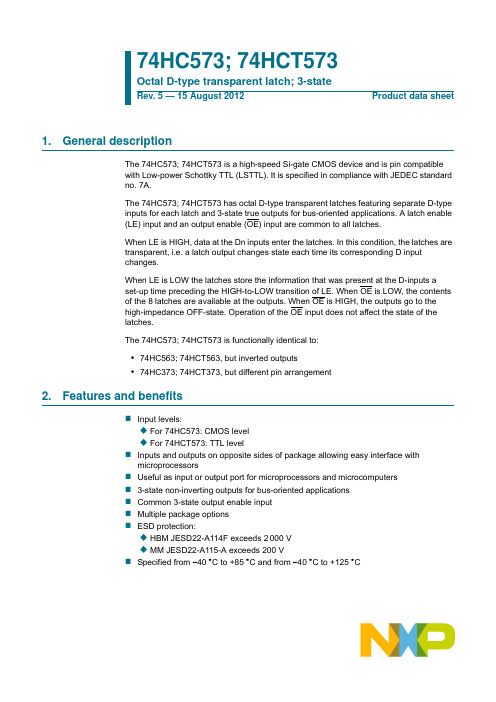
Fig 5.
Pin configuration DIP20, SO20, SSOP20 and TSSOP20
Fig 6.
Pin configuration DHVQFN20
5.2 Pin description
Table 2. Symbol OE D[0:7] GND LE Q[0:7] VCC Pin description Pin 1 2, 3, 4, 5, 6, 7, 8, 9 10 11 20 Description 3-state output enable input (active LOW) data input ground (0 V) latch enable input (active HIGH) supply voltage
• 74HC563; 74HCT563, but inverted outputs • 74HC373; 74HCT373, but different pin arrangement
2. Features and benefits
Input levels: For 74HC573: CMOS level For 74HCT573: TTL level Inputs and outputs on opposite sides of package allowing easy interface with microprocessors Useful as input or output port for microprocessors and microcomputers 3-state non-inverting outputs for bus-oriented applications Common 3-state output enable input Multiple package options ESD protection: HBM JESD22-A114F exceeds 2 000 V MM JESD22-A115-A exceeds 200 V Specified from 40 C to +85 C and from 40 C to +125 C
- 1、下载文档前请自行甄别文档内容的完整性,平台不提供额外的编辑、内容补充、找答案等附加服务。
- 2、"仅部分预览"的文档,不可在线预览部分如存在完整性等问题,可反馈申请退款(可完整预览的文档不适用该条件!)。
- 3、如文档侵犯您的权益,请联系客服反馈,我们会尽快为您处理(人工客服工作时间:9:00-18:30)。
3.6
⎯
⎯ ±0.25 ⎯ ±2.5 μA
IIN VIN = 5.5 V or GND
3.6
⎯
⎯ ±0.1 ⎯ ±1.0 μA
ICC VIN = VCC or GND
3.6
⎯
⎯
4.0
⎯ 40.0 μA
Timing Requirements (input: tr = tf = 3 ns)
Characteristics
tpHL
3.3 ± 0.3
50
⎯
8.4 12.8 1.0 14.5
Output enable time
tpZL tpZH
RL = 1 kΩ
15 2.7
LE
C1
(2)
D0
1D
(3) D1
(4) D2
(5) D3
(6) D4
(7) D5
(8) D6
(9) D7
(19) Q0
(18) Q1
(17) Q2
(16) Q3
(15) Q4
(14) Q5
(13) Q6
(12) Q7
Truth Table
Inputs
OE
LE
D
H
X
X
L
L
X
L
H
L
L
H
H
Outputs
2.0
1.5
⎯
⎯
1.5
⎯
VIH
⎯
3.0
2.0
⎯
⎯
2.0
⎯
3.6
2.4
⎯
⎯
2.4
⎯
V
2.0
⎯
⎯
0.5
⎯
0.5
VIL
⎯
3.0
⎯
⎯
0.8
⎯
0.8
3.6
⎯
⎯
0.8
⎯
0.8
IOH = −50 μA 2.0
1.9 2.0
⎯
1.9
⎯
VOH
VIN = VIH or VIL
IOH = −50 μA
3.0
2.9 3.0
OE 1 D0 2 D1 3 D2 4 D3 5 D4 6 D5 7 D6 8 D7 9 GND 10
20 VCC 19 Q0 18 Q1 17 Q2 16 Q3 15 Q4 14 Q5 13 Q6 12 Q7 11 LE
TC74LVX573F/FT
IEC Logic Symbol
(1)
OE
EN
(11)
VCC VIN VOUT IIK IOK IOUT ICC PD Tstg
−0.5 to 7.0
V
−0.5 to 7.0
V
−0.5 to VCC + 0.5
V
−20
mA
±20
mA
±25
mA
±75
mA
180
mW
−65 to 150
°C
Note: Exceeding any of the absolute maximum ratings, even briefly, lead to deterioration in IC performance or even destruction. Using continuously under heavy loads (e.g. the application of high temperature/current/voltage and the significant change in temperature, etc.) may cause this product to decrease in the reliability significantly even if the operating conditions (i.e. operating temperature/current/voltage, etc.) are within the absolute maximum ratings and the operating ranges. Please design the appropriate reliability upon reviewing the Toshiba Semiconductor Reliability Handbook (“Handling Precautions”/“Derating Concept and Methods”) and individual reliability data (i.e. reliability test report and estimated failure rate, etc).
Z Qn L H
X: Don’t care Z: High impedance Qn: Q outputs are latched at the time when the LE input is taken to a low logic level.
System Diagram
D0 2
D
D1 3
D
ห้องสมุดไป่ตู้
3
芯天下--/
2007-10-17
TC74LVX573F/FT
Electrical Characteristics
DC Characteristics
Characteristics
Input voltage
H-level L-level
Output voltage
H-level L-level
3-state output Off-state current Input leakage current Quiescent supply current
Symbol
Test Condition
Ta = 25°C
Ta = −40 to
85°C
Unit
VCC (V) Min Typ. Max Min Max
2.0 to 3.6 0 to 5.5 0 to VCC −40 to 85 0 to 100
V V V °C ns/V
Note: The operating ranges must be maintained to ensure the normal operation of the device. Unused inputs must be tied to either VCC or GND.
Operating Ranges (Note)
Characteristics
Symbol
Rating
Unit
Supply voltage Input voltage Output voltage Operating temperature Input rise and fall time
VCC VIN VOUT Topr dt/dv
Features
• High speed: tpd = 6.4 ns (typ.) (VCC = 3.3 V) • Low-power dissipation: ICC = 4 μA (max) (Ta = 25°C) • Input voltage level: VIL = 0.8 V (max) (VCC = 3 V)
⎯
2.9
⎯
IOH = −4 mA
3.0
2.58
⎯
⎯ 2.48 ⎯
V
IOL = 50 μA
2.0
⎯
0
0.1
⎯
0.1
VOL
VIN = VIH or VIL
IOL = 50 μA
3.0
⎯
0
0.1
⎯
0.1
IOL = 4 mA
3.0
⎯
⎯ 0.36 ⎯ 0.44
VIN = VIH or VIL IOZ
VOUT = VCC or GND
ns
15
⎯
6.4 10.1 1.0 12.0
tpHL
3.3 ± 0.3
50
⎯
8.9 13.6 1.0 15.5
Propagation delay time (D-Q)
15
⎯
7.6 14.5 1.0 17.5
tpLH
2.7
50
⎯ 10.1 18.0 1.0 21.0
⎯
ns
15
⎯
5.9
9.3
1.0 11.0
This device is suitable for low-voltage and battery operated systems.
This 8 bit D-type latch is controlled by a latch enable input (LE) and an output enable input ( OE ). When the OE input is high, the eight outputs are in a high-impedance state.
TC74LVX573F/FT
TOSHIBA CMOS Digital Integrated Circuit Silicon Monolithic
TC74LVX573F,TC74LVX573FT
Octal D-Type Latch with 3-State Output
The TC74LVX573F/ FT is a high-speed CMOS octal latch with 3-state output fabricated with silicon gate CMOS technology. Designed for use in 3-V systems, it achieves high-speed operation while maintaining the CMOS low power dissipation.