OB2216
OB2216 Datasheet

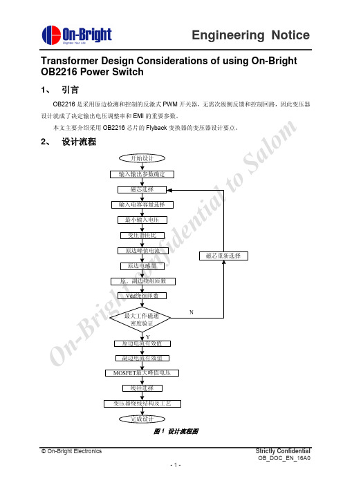
OB2216Primary-Side Regulation PWM Power SwitchGENERAL DESCRIPTIONOB2216 is an offline PWM Power switch for low power AC/DC charger and adaptor applications. It operates in primary-side sensing and regulation. Consequently, opto-coupler and TL431 could be eliminated. Proprietary Constant Voltage (CV) and Constant Current (CC) control is integrated as shown in the figure below.In CC control, the current and output power setting can be adjusted externally by the sense resistor Rs at CS pin. In CV control, multi-mode operations are utilized to achieve high performance and highefficiency. Device operates in fixed frequency mode at large load conditions, frequency reduction mode at light/medium load and ‘Extended burst mode’ at No/light load conditions.OB2216 offers power on soft start control andprotection coverage with auto-recovery features including Cycle-by-Cycle current limiting, VDD clamp and UVLO. Excellent EMI performance is achieved with On-Bright proprietary frequency shuffling technique together with soft switching control at the totem pole gate drive output.Fig 1. Typical CC/CV CurveFEATURESPrimary-side Sensing and Regulation WithoutTL431 and Opto-couplerMulti-mode Operation for High Efficiency Programmable CV and CC RegulationAdjustable Constant Current and Output PowersettingFrequency Shuffling and Adjustable Gate DriveGreatly Improving EMIPower on Soft-start Time (4ms)“Extended Burst Mode Control” for ImprovedEfficiency and Minimum Standby Design Built-in Leading Edge Blanking (LEB) Cycle-by-Cycle Current LimitingVDD Under Voltage Lockout with Hysteresis(UVLO) VDD ClampAPPLICATIONSLow Power AC/DC offline SMPS forCell Phone ChargerDigital Cameras Charger Small Power AdaptorAuxiliary Power for PC, TV etc. Linear Regulator/RCC ReplacementOB2216 is offered in DIP8 packageTYPICAL APPLICATIONOB2216Primary-Side Regulation PWM Power SwitchGENERAL INFORMATIONPin ConfigurationThe pin map is shown as below for DIP8.Ordering InformationPart Number DescriptionOB2216AP DIP8,Pb-freeAbsolute Maximum RatingsParameter ValueDrain Voltage (off state) -0.3V to BvdssVDD Voltage -0.3 to V DD_clampVDDG Voltage -0.3 to V DD_clampVDD Zener ClampContinuous Current10 mACS Input Voltage -0.3 to 7VINV Input Voltage -0.3 to 7VMin/Max OperatingJunction Temperature T J-20 to 150 oCMin/Max StorageTemperature T stg-55 to 150 o CLead Temperature(Soldering, 10secs)260 o CNote: Stresses beyond those listed under “absolute maximumratings” may cause permanent damage to the device. These arestress ratings only, functional operation of the device at these orany other conditions beyond those indicated under “recommendedoperating conditions” is not implied. Exposure to absolutemaximum-rated conditions for extended periods may affect devicereliability.OB2216Primary-Side Regulation PWM Power SwitchMarking InformationTERMINAL ASSIGNMENTSPin Num Pin Name I/O Description1 VDDG P Internal Gate Driver Power Supply2 VDD P IC DC power supply Input3 INVIInverting input of error amplifier (EA). Connected to resistor divider fromprimary sensing winding reflecting output voltage. PWM duty cycle isdetermined by EA output and current sense signal at pin 4.4 CS I Current sense input5/6 Drain OHV MOSFET Drain Pin. The Drain pin is connected to the primary lead ofthe transformer7/8 GND PGroundOutput Power Table230VAC±15% 85-264VAC ProductOpen Frame1 Open Frame1OB2216 20W 15WNotes:1. Maximum practical continuous power in an open frame design with sufficient drain pattern as a heat sink, at 50℃ ambient.BLOCK DIAGRAMELECTRICAL CHARACTERISTICS(T A = 25O C, VDD=VDDG=16V, if not otherwise noted) Symbol Parameter Test Conditions Min Typ Max Unit Supply Voltage (VDD) SectionI DD ST Standby CurrentVDD=13.5V 5 10uA I DD op Operation Current Operation supply current INV=1.25V, CS=0V, VDD=VDDG=20V - 1.02.0 mA UVLO(ON) VDD Under Voltage Lockout Enter7.5 8.5 9.5VUVLO(OFF)VDD Under Voltage Lockout Exit14.0 15 16.0VV DD _clamp I DD =10mA 38 V Current Sense Input SectionT LEB LEB time540 ns Vth_oc V th _OCtest780 820 860 mV Td_oc Propagation delay 110 ns Z SENSE _IN Input Impedance 50 Kohm T_ss Soft start time4msCV Section Freq Normal mode frequency 45 50 55 KHzFreq_Burst Burst Mode Base Frequency 22KHz△f/Freq Frequency shuffling range+/-4 %CC SectionMinimum frequency 12 KHz Freq Oscillation FrequencyMaximum frequency 50 KHz Error Amplifier section Vref_EA Reference voltage for EA 1.21 1.25 1.29 V Gdc DC gain of the EA 50 dB GBWUnity gain bandwidth37.5kHzPower MOSFET Section BVdssMOSFET Off-state Drain-Source Breakdown600 VRdson Static, Id =0.9A4.45.5 ΏCHARACTERIZATION PLOTSOPERATION DESCRIPTIONOB2216 is cost effective PWM power switch optimized for off-line low power AC/DC applications including battery chargers and adaptors. It operates in primary side sensing and regulation, thus opto-coupler and TL431 are not required. Proprietary CC control and built-in error amplifier can achieve a good CC/CV performance.z Startup Current and Start up Control Startup current of OB2216 is designed to be very low so that VDD could be charged up above UVLO threshold and starts up quickly. A large value startup resistor can therefore be used to minimize the power loss in application.z Operating CurrentThe Operating current of OB2216 is as low as 1mA. Good efficiency is achieved with the low operating current together with ‘Extended burst mode’ control features.z Soft StartOB2216 features an internal 4ms soft start to minimize the component electrical over-stress during power on startup. As soon as VDD reaches UVLO(OFF), the control algorithm will ramp peak current voltage threshold gradually from nearly zero to normal setting of 0.82V. Every restart is a soft start.z CC/CV OperationOB2216 is designed to produce good CC/CV control characteristic as shown in the Fig. 1.In charger applications, a discharged battery charging starts in the CC portion of the curve until it is nearly full charged and smoothly switches to operate in CV portion of the curve.In an AC/DC adapter, the normal operation occurs only on the CV portion of the curve. The CC portion provides output current limiting. In CV operation, the output voltage is regulated through the primary side control.To support OB2216 proprietary CC/CV control, system needs to be designed in DCM mode for flyback system. Under normal operation, when INV is less than Vref, the system works in CC control, Otherwise, the system works in CV control.z Error Amplifier (EA)Connected to a resistor divider from the primary side sensing winding, the inverting input of the Error Amplifier (EA) is compared to an internal reference voltage of 1.25V to regulate the output voltage. The EA output is internally connected to the PWM generator and controls the duty cycle.z Adjustable CC point and Output PowerIn OB2216, the CC point and output power can be externally adjusted by external current sense resistor Rs at CS pin. The output power is adjusted through CC point change. The larger Rs, the smaller CC point is, and the smalleroutput power becomes, and vice versa as shown in Fig.2.Fig. 2 Adjustable output power by changing Rsz Extended Burst Mode OperationAt light load or zero load condition, most of the power dissipation in a switching mode power supply is from switching loss, the core loss of the transformer and the loss on the snubber circuit. The magnitude of power loss is in proportion to the switching frequency. Lower switching frequency leads to the reduction on the power loss and thus conserves the energy.OB2216 self adjusts the switching frequency according to the loading condition. The switch frequency is reduced at light/no load condition to improve the conversion efficiency. At light load/no load condition, the output of the Error amplifier (EA) drops below the burst mode threshold level and device enters Burst Mode control. The frequency control also eliminates the audio noise at any loading conditions.z Operation switching frequencyThe switching frequency of OB2216 is adaptively controlled according to CC/CV operation. No external frequency setting components are required.z Frequency shuffling for EMI improvement The frequency Shuffling (switching frequency modulation) is implemented in OB2216. The oscillation frequency is modulated so that the tone energy is spread out. The spread spectrum minimizes the conduction band EMI and therefore eases the system design.z Current Sensing and Leading Edge Blanking Cycle-by-Cycle current limiting is offered in OB2216 current mode PWM control. The switch current is detected by a sense resistor into the CS pin. An internal leading edge blanking circuit chops off the sensed voltage spike at initial internal power MOSFET on state so that the external RC filtering on sense input is no longer needed. The PWM duty cycle is determined by the current sense input voltage and the EA output voltage. z Adjustable Drive CapabilityThe internal power MOSFET in OB2216 is driven by a dedicated gate driver for power switch control. Too weak the gate drive strength results in higher conduction and switch loss of MOSFET while too strong gate drive compromises EMI.A good tradeoff is achieved through the built-in totem pole gate design with right output strength control. The gate drive strength can be adjusted externally by a resistor connected between VDD and VDDG. The low idle loss and good EMI system design is possible with this dedicated control scheme. z Protection ControlGood power supply system reliability is achieved with its rich protection features including Cycle-by-Cycle current limiting (OCP), VDD protection and clamp, Power on Soft Start, and Under Voltage Lockout on VDD (UVLO).VDD is supplied by transformer auxiliary winding output. The output of OB2216 is shut down when VDD drops below UVLO(ON) limit and Switcher enters power on start-up sequence thereafter.PACKAGE MECHANICAL DATADimensions In Millimeters Dimensions In Inches SymbolMin Max Min MaxA 3.710 4.310 0.146 0.1700.500 0.020A1A2 3.200 3.600 0.126 0.142B 0.350 0.650 0.014 0.026B1 1.524 (BSC) 0.060 (BSC)C 0.200 0.360 0.008 0.014D 9.000 9.500 0.354 0.374E 6.200 6.600 0.244 0.260E1 7.320 7.920 0.288 0.312e 2.540 (BSC) 0.100 (BSC)L 3.000 3.600 0.118 0.142 E2 8.200 9.000 0.323 0.354IMPORTANT NOTICERIGHT TO MAKE CHANGESOn-Bright Electronics Corp. reserves the right to make corrections, modifications, enhancements, improvements and other changes to its products and services at any time and to discontinue any product or service without notice. Customers should obtain the latest relevant information before placing orders and should verify that such information is current and complete.WARRANTY INFORMATIONOn-Bright Electronics Corp. warrants performance of its hardware products to the specifications applicable at the time of sale in accordance with its standard warranty. Testing and other quality control techniques are used to the extent it deems necessary to support this warranty. Except where mandated by government requirements, testing of all parameters of each product is not necessarily performed.On-Bright Electronics Corp. assumes no liability for application assistance or customer product design. Customers are responsible for their products and applications using On-Bright’s components, data sheet and application notes. To minimize the risks associated with customer products and applications, customers should provide adequate design and operating safeguards.LIFE SUPPORTOn-Bright Electronics Corp.’s products are not designed to be used as components in devices intended to support or sustain human life. On-bright Electronics Corp. will not be held liable for any damages or claims resulting from the use of its products in medical applications.MILITARYOn-Bright Electronics Corp.’s products are not designed for use in military applications. On-Bright Electronics Corp. will not be held liable for any damages or claims resulting from the use of its products in military applications.。
九年级上册数学同步练习含答案大全

九年级上册数学同步练习含答案大全数学是人类对事物的抽象结构与模式进行严格描述的一种通用手段,可以应用于现实世界的任何问题,全部的数学对象本质上都是人为定义的。
下面是我为大家整理的关于九年级上册数学同步练习含答案,希望对您有所关怀!九年级数学第21章同步测试题与答案二次根式(第二课时)随堂检测1、化简| -2|+ 的结果是( )A.4-2B.0C.2D.42、以下各式中,确定能成立的是( )A. B.C. D.3、已知xy,化简 p= 为_______.4、若,则 _________;若,则 ________.5、当时,求|2- |的值是多少?典例分析有一道练习题是:对于式子先化简,后求值.其中 .小明的解法如下: = = = = .小明的解法对吗?假如不对,请改正.分析:此题中有一个隐含条件,即,并由此应将化简为 .对这个隐含条件的敏感度是正确解决问题的关键.解:小明的解法对不对.改正如下:由题意得,,∴应有 .∴ = = = = .课下作业拓展提高1、当-1 1时,化简得( )A.2B.-2C.2D.-22、计算 =_______.3、观看以下各式:请你将觉察的规律用含自然数n(n≥1)的等式表示出来 .4、把以下非负数写成一个数的平方的形式:(1)5 (2)3.4 (3) (4)x(x≥0)5、在实数范围内分解以下因式:(1) (2) (3)6、已知实数满足,求的值是多少?体验中考1、(2021年,长沙)已知实数在数轴上的位置如下列图,则化简的结果为( )A.1B.-1C.D.(留意:由图可知,我们可以直接利用这个结论解题.)2、(2021年,广州)实数在数轴上的位置如下列图,化简 .(提示:由图可知,可以选择利用和解题.)参考答案:随堂检测1、A. ∵ 有意义,∴ ,∴原式= ,应选A.2、A. ∵只有A选项不含代数字母,等式总成立.应选A.3、0. ∵x4、,∵当时,由得 ;当时,由得,即 .5、解:当时, , ,∴|2- |=|2- |=| |= .课下作业拓展提高1、A. ∵当-1 1时,∴ , ,∴ ,应选A.2、可以直接利用 ( )的结论解题. = .3、 = .4、解:(1)5=( )2 (2)3.4=( )2(3) =( )2 (4)x=( )2(x≥0).5、解:(1)(2)(3)6、解:∵实数满足,∴ ,∴ ,∴ ,∴由可得:,化简得:,∴ ,∴ .体验中考1、A 由题图可知,∴ ,∴原式= ,应选A.2、由图可知,∴原式= .九年级上册数学练习带答案一、选择题(在以下各题的四个备选答案中,只有一个是符合题意的,请将正确答案前的字母写在答题纸上;此题共32分,每题4分)1. 已知⊙O的直径为3cm,点P到圆心O的距离OP=2cm,则点PA. 在⊙O外B. 在⊙O上C. 在⊙O内D. 不能确定2. 已知△ABC中,∠C=90°,AC=6,BC=8,则cosB的值是A.0.6B.0.75C.0.8D.3.如图,△ABC中,点 M、N分别在两边AB、AC上,MN‖BC,则以下比例式中,不正确的选项是A .B .C. D.4. 以下列图形中,既是中心对称图形又是轴对称图形的是A. B. C. D.5. 已知⊙O1、⊙O2的半径分别是1cm、4cm,O1O2= cm,则⊙O1和⊙O2的位置关系是A.外离B.外切C.内切D.相交6. 某二次函数y=ax2+bx+c 的图象如下列图,则以下结论正确的选项是A. a0, b0, c0B. a0, b0, c0C. a0, b0, c0D. a0, b0, c07.以下命题中,正确的选项是A.平面上三个点确定一个圆B.等弧所对的圆周角相等C.平分弦的直径垂直于这条弦D.与某圆一条半径垂直的直线是该圆的切线8. 把抛物线y=-x2+4x-3先向左平移3个单位,再向下平移2个单位,则变换后的抛物线解析式是A.y=-(x+3)2-2B.y=-(x+1)2-1C.y=-x2+x-5D.前三个答案都不正确二、填空题(此题共16分, 每题4分)9.已知两个相像三角形面积的比是2∶1,则它们周长的比 _____ .10.在反比例函数y= 中,当x0时,y 随 x的增大而增大,则k 的取值范围是_________.11. 水平相当的甲乙两人进行羽毛球竞赛,规定三局两胜,则甲队战胜乙队的概率是_________;甲队以2∶0战胜乙队的概率是________.12.已知⊙O的直径AB为6cm,弦CD与AB相交,夹角为30°,交点M恰好为AB的一个三等分点,则CD的长为 _________ cm.三、解答题(此题共30分, 每题5分)13. 计算:cos245°-2tan45°+tan30°- sin60°.14. 已知正方形MNPQ内接于△ABC(如下列图),若△ABC的面积为9cm2,BC=6cm,求该正方形的边长.15. 某商场预备改善原有自动楼梯的安全性能,把倾斜角由原来的30°减至25°(如下列图),已知原楼梯坡面AB的长为12米,调整后的楼梯所占地面CD 有多长?(结果精确到0.1米;参考数据:sin25°≈0.42,cos25°≈0.91,tan25°≈0.47)16.已知:△ABC中,∠A是锐角,b、c分别是∠B、∠C的对边.求证:△ABC的面积S△ABC= bcsinA.17. 如图,△ABC内接于⊙O,弦AC交直径BD于点E,AG⊥BD于点G,延长AG交BC于点F. 求证:AB2=BF•BC.18. 已知二次函数 y=ax2-x+ 的图象经过点(-3, 1).(1)求 a 的值;(2)推断此函数的图象与x轴是否相交?假如相交,请求出交点坐标;(3)画出这个函数的图象.(不要求列对应数值表,但要求尽可能画精确)四、解答题(此题共20分, 每题5分)19. 如图,在由小正方形组成的12×10的网格中,点O、M和四边形ABCD 的顶点都在格点上.(1)画出与四边形ABCD关于直线CD对称的图形;(2)平移四边形ABCD,使其顶点B与点M重合,画出平移后的图形;(3)把四边形ABCD绕点O逆时针旋转90°,画出旋转后的图形.20. 口袋里有 5枚除颜色外都相同的棋子,其中 3枚是红色的,其余为黑色.(1)从口袋中随机摸出一一枚棋子,摸到黑色棋子的概率是_______ ;(2)从口袋中一次摸出两枚棋子,求颜色不同的概率.(需写出“列表”或画“树状图”的过程)21. 已知函数y1=- x2 和反比例函数y2的图象有一个交点是 A( ,-1).(1)求函数y2的解析式;(2)在同始终角坐标系中,画出函数y1和y2的图象草图;(3)借助图象回答:当自变量x在什么范围内取值时,对于x的同一个值,都有y122. 工厂有一批长3dm、宽2dm的矩形铁片,为了利用这批材料,在每一块上裁下一个最大的圆铁片⊙O1之后(如下列图),再在剩余铁片上裁下一个充分大的圆铁片⊙O2.(1)求⊙O1、⊙O2的半径r1、r2的长;(2)能否在剩余的铁片上再裁出一个与⊙O2 同样大小的圆铁片?为什么?五、解答题(此题共22分, 第23、24题各7分,第25题8分)23.如图,在△ABC中,AB=AC,以AB为直径的⊙O分别交AC、BC于点M、N,在AC的延长线上取点P,使∠CBP= ∠A.(1)推断直线BP与⊙O的位置关系,并证明你的结论;(2)若⊙O的半径为1,tan∠CBP=0.5,求BC和BP的长.24. 已知:如图,正方形纸片ABCD的边长是4,点M、N分别在两边AB和CD上(其中点N不与点C重合),沿直线MN折叠该纸片,点B恰好落在AD边上点E处.(1)设AE=x,四边形AMND的面积为 S,求 S关于x 的函数解析式,并指明该函数的定义域;(2)当AM为何值时,四边形AMND的面积最大?最大值是多少?(3)点M能是AB边上任意一点吗?请求出AM的取值范围.25. 在直角坐标系xOy 中,已知某二次函数的图象经过A(-4,0)、B(0,-3),与x轴的正半轴相交于点C,若△AOB∽△BOC(相像比不为1).(1)求这个二次函数的解析式;(2)求△ABC的外接圆半径r;(3)在线段AC上是否存在点M(m,0),使得以线段BM为直径的圆与线段AB 交于N点,且以点O、A、N为顶点的三角形是等腰三角形?若存在,求出m的值;若不存在,请说明理由.一、 ACCB DABB二、 9. :1 10. k -1 11. , 12.三、13. 原式= -2+ - ×= -2 + - ……………………………………4分= -3+ ……………………………………………………5分14. 作AE⊥BC于E,交MQ于F.由题意,BC×AE=9cm2 , BC=6cm.∴AE=3cm. ……………………………1分设MQ= xcm,∵MQ‖BC,∴△AMQ∽△ABC. ……………………2分∴ . ……………………3分又∵EF=MN=MQ,∴AF=3-x.∴ . ……………………………………4分解得 x=2.答:正方形的边长是2cm. …………………………5分15. 由题意,在Rt△ABC中,AC= AB=6(米), …………………1分又∵在Rt△ACD中,∠D=25°,=tan∠D, ……………………………3分∴CD= ≈ ≈12.8(米).答:调整后的楼梯所占地面CD长约为12.8米. ……………………5分 16. 证明:作CD⊥AB于D,则S△ABC= AB×CD. ………………2分∵ 不管点D落在射线AB的什么位置,在Rt△ACD中,都有CD=ACsinA. …………………4分又∵AC=b,AB=c,∴ S△ABC= AB×A九年级数学上册练习题及答案一选择题:1、以下命题中的真命题是、A、对角线互相垂直的四边形是菱形B、中心对称图形都是轴对称图形C、两条对角线相等的梯形是等腰梯形D、等腰梯形是中心对称图形第2题图2、如右图,将半径为2cm的圆形纸片折叠后,圆弧恰好经过圆心O,则折痕AB的长为 A.2cmB.3cm C.23cm D.25cm3、如图,BD是⊙O的直径,∠CBD=30?,则∠A的度数.A、30?B、45?C、60?D、75?、已知二次函数y=ax2+bx+c的图像如下列图,则以下条件正确的选项是 A.ac0B、b-4ac0C、 b0D、 a0,b0,c05、抛物线y= x 向左平移8个单位,再向下平移个单位后,所得抛物线的表达式是A、 y=2-B、 y=2+C、 y=2-D、 y=2+96.如图,在平面直角坐标系中,长、宽分别为2和1的矩形ABCD的边上有一动点P,沿A→B→C→D→A运动一周,则点P的纵坐标y与P所走过的路程x之间的函数关系用图象表示大致是2第3题图第4题图7、某商品原售价289元,经过连续两次降价后售价为256元,设平均每次降价的百分率为 x,则下面所列方程中正确的选项是A、2892=25B、2562=289C、289=25D、256=2898、如图,在平面直角坐标系中,正方形ABCD的顶点A、C分别在y 轴、x轴上,以AB为弦的⊙M与x轴相切、若点A的坐标为,则圆心M的坐标为A、B、C、D、9.若点A的坐标为O为坐标原点,将OA绕点O按顺时针方向旋转90得到OA′,则点A′的坐标是A、B、C、D、10、以下各点中,在函数y=-6x 图像上的是12A、B、C、D、11.抛物线y=x?2x?3与坐标轴交点为 A.二个交点 B.一个交点 C.无交点D.三个交点12.关于x的一元二次方程x2+x+m+1=0有两个相等的实数根,则m 的值是A、0B、C、422D、 0或二、填空题:13 、使x的取值范围是、 A DB E D14、将二次函数y=x2-4x+5化为y=2+k的形式,则15 、如下列图,把一个长方形纸片沿EF折叠后,点D,C分别落 CC 在D′,C′的位置.若∠EFB=65,则∠AED′等于16、菱形OABC在平面直角坐标系中的位置如下列图, ?AOC?45,OC?B的坐标为.17、如下列图,边长为1的小正方形构成的网格中,半径为1的⊙O的圆心O在格点上,则∠AED的正切值等于、三、解答题:18、解方程:2 x+6x-11=019、如图,在平面直角坐标系中,△ABC的三个顶点的坐标分别为A,B,C、、画出△ABC关于x轴对称的△A1B1C1,并写出点C1的坐标; 、画出△ABC绕原点O顺时针方向旋转90后得到的△A2B2C2,并写出点C2的坐标;,第16B A C第17题图将△A2B2C2平移得到△ A3B3C3,使点A2的对应点是A3,点B2的对应点是B3,点C2的对应点是C3,在坐标系中画出△ A3B3C3,并写出点A3的坐标。
Engineering Notice(昂宝)
4.14
变压器绕线结构及工艺
copper 隔离→原边绕组 pri→ copper 隔离→输出绕组 sec→4T Tape 隔离→辅助绕组 Vdd
5
A N1 N2
3 1
N3
4
O
n-
Br ig ht
© On-Bright Electronics -7-
co nf
图 2 变压器电气原理图
图 3 变压器绕制顺序图
3.14
根据输入输出电流有效值确定变压器原、副边绕组线径,一般取电流密度为 5A/mm2。
3.15
变压器会因为绕组绕制方式不同而在电气特性和 EMI 上有很大差别,尤其是对于采用原边控制的 OB2216 芯片,需要注意以下三点: 1) 为了提高输出电压负载调整率,希望特别注意输出绕组和辅助反馈绕组的耦合度 2) 为了减小漏感,还需要注意原边绕组和输出绕组之间耦合度,但是 EMI 的考虑却同以上相反, 原边绕组和辅助反馈绕组同属于一次侧绕组, 输出绕组输出二次侧绕组, 为了更好的 EMI 特性, 要求一次侧绕组和二次测绕组之间有一定的间隔 3) 各绕组每一层要绕满,如果不满,可以采用减小线径,多股并饶的方式
(17)
在实际测试过程中,为了提高效率,可以适当增大电感量,取在 Lm=1.8mH~2.0mH,原边峰值电 流 Ipk 会适当降低。
4.8
原边、副边绕组匝数
原边绕组匝数为:
Np =
Ae ⋅ ΔB
=
Sa to ia l
VDCMIN ⋅ Ton _ max
88 ⋅ 9.6 ≈ 120T 33.5 ⋅ 2100
2 V DCMIN = Vac min_ pk
⎛T ⎞ 2 ⋅ Pin ⋅ ⎜ − Tc ⎟ ⎝2 ⎠ = − Cin
2216e培养基作用
2216e培养基作用2216e培养基(2216e Medium)是一种常用的微生物培养基,广泛应用于细菌和真菌的培养及研究。
本文将介绍2216e培养基的组成、作用及其在微生物学领域中的应用。
一、2216e培养基的组成2216e培养基由多种成分组成,主要包括蛋白胨、酵母提取物、海藻提取物等。
蛋白胨是一种富含氨基酸和多肽的蛋白质水解物,提供微生物所需的碳源和氮源。
酵母提取物则富含维生素、脂肪酸和微量元素,为微生物提供必要的营养物质。
海藻提取物富含多种有机物,可提供微生物所需的微量元素和生长因子。
二、2216e培养基的作用2216e培养基具有以下几个作用:1. 提供营养物质:2216e培养基中的蛋白胨、酵母提取物等能够为微生物提供必要的碳源、氮源、维生素和微量元素,满足微生物的生长和繁殖需求。
2. 促进微生物生长:培养基中的蛋白胨和酵母提取物等富含的营养物质可以刺激微生物的生长,提供足够的能量和营养物质,促进微生物的繁殖。
3. 增加微生物产物产量:2216e培养基中的成分经过精心配比,可以为微生物提供适宜的生长环境,促进微生物代谢产物的积累和生产。
三、2216e培养基的应用2216e培养基在微生物学领域中有着广泛的应用,主要包括以下几个方面:1. 微生物的分离和纯化:2216e培养基中的丰富营养物质可以满足微生物的生长需求,使微生物得以繁殖和生长。
通过在2216e培养基上进行微生物的分离培养,可以获得纯种菌株,用于后续的研究和应用。
2. 微生物的培养和增殖:2216e培养基提供了适宜的环境和养分,可以促进微生物的生长和增殖。
通过在2216e培养基上进行微生物的大规模培养,可以获得足够的微生物量,用于生产菌种、酶制剂等。
3. 微生物代谢产物的研究:2216e培养基中的成分经过优化配比,可以刺激微生物的代谢,促进代谢产物的积累。
通过在2216e培养基上进行微生物的培养,可以研究微生物的代谢途径、产物合成等,为后续的药物开发和工业应用提供依据。
血液检验血常规检验英文缩写

.血液检验血常规检验英文缩写、参考值检验项目英文缩写参考值范围1/L14.5-5.51/L13.5-5.0RBC红细胞计1/L5.2-7.01新生1/L4.2-5.21儿120-165g/L110-155g/LHb,Hgb血红蛋新生160-220g/L儿110-160g/L0.420-0.490红细胞压Hb,Hgb0.370-0.440新生0.350-0.440红细胞平均体MCV80-98fl28-32pg红细胞平均血红蛋MCH32-36%MCHC红细胞平均血红蛋白浓成0.5-1.5%网织红细胞计Ret.C2.0-6.0%新生血小板计LPL100-3501BPC MPV6.0-1.5fl平均血小板体/L14.0-10.0成/L5.0-12.0白细胞计WBC儿1/L10.0-22.01新生50-70%;中性分叶核粒细1-4%;中性杆状核粒细1-4%;嗜酸性粒细WBCDC成白细胞分类计)0-1%;嗜碱性粒细20-35%;淋巴细1-6%单核细30-65%;中性分叶核粒细3-8%;中性杆状核粒细1-4%;嗜酸性粒细WBCDC白细胞分类计儿)0-1%;嗜碱性粒细30-65%;淋巴细1-6%单核细胞'..9/L 0.05-0.3×10嗜酸性粒细胞直接计数Eos.c 分钟BT 1-3出血时间CT 分钟1-4凝血时间玻片法)管时间为分5-1凝血时间试管以CCT血块收缩时2CRT小时完全收第一小魏氏法:男<15mmESR红细胞沉降<20mm第一小女)反应呈绿褐阴一氧化碳定性实)反应呈橙红阳以上同血细胞检查正常HCRB包WBHGBCA 全血细胞分PLT)MCHCMCH尿常规检验英文缩写、参考14:00:31发表2006-7-6labsky异常结果参考正常参考英项目名>1.030SG<1.011.010 - 1.030比>8<5 - 8酸碱PH15 70 125 500NEGATIVE25 75 100 300 500negLEU白细5-10 10-1520-40 >50镜检:0 - 5/HPFNEGATIVEPOS亚硝酸盐NITnegSPUR 30100 ...>=300NEGATIVE...25 75 150 500 尿蛋白PROneg++ +++-- ++++ ±约±...00 250 500 >=1000NEGATIVEGLU尿糖50100 300 (1000)norm'..+++ +++--++++ 微量约±SPUR 15 40 >=80NEGATIVE5 15 50 150KET酮体neg+ ++ +++1.0 2.0 4.0 80.2UBG尿胆1... 4 8 12normSCHWACHMAESSIGSTARKNRGATIVEBIL尿胆红1 36neg1025 80... 200NEGATIVE红潜/1025 50 150250OBL / ERYneg0-5 2-68-1520-30 >400-3/HPF镜检生化检验英文缩写、参考14:01:462006-7-6labsky发表于参考值范英文缩检查项6.11mmol/L血3.8Glu7.2mmol/LUREA尿3.0420 umol/L~男性:210成人350 umol/L ~女性:150尿酸UA320 umol/L 120~儿童80 umol/L 44~男:Cr肌酐~115 umol/L 女:70-CP CO20-34mmoI/L 二氧化碳结合力2K 钾3.5-5.5mmol/LNa 135-45mmol/L 钠CL96-106mmol/L氯化物2.54 mmol/L 2.03~成人Ca钙 2.67 mmol/L ~儿童2.251.62 mmol/L 0.96 ~成人P磷 2.10 mmol/L儿童1.45 ~'..<220u/LAMS 淀粉酶5.17 mmol/L ~胆固醇2.23Chol1.60 g/L ~ApoAI 载脂蛋白A1 ApoAI 1.001.10 g/L ApoB ~B 载脂蛋白ApoB 0.61.69 mmol/LTG0.5甘油三18~196u/LCK肌酸激1.45 mmol/L0.9HDL-C高密度脂蛋1.68 mmol/L1.1LDL-C低密度脂蛋4.0 mmol/L1.T-BIL 5.总胆红22 umol/lD-BIL直接胆红6.8 umol/l1.SGPT/ALT<40u/L丙氨酸氨基转移谷丙转氨天门冬氨酸氨基转谷草转氨<35u/LSGOT/AST97-270Iu/L乳酸脱氢LDH72-182Iu/L-HBDH羟丁酸脱氢27-107u/L碱性磷酸ALP<4.7ACP酸性磷酸<3.710~50u/L-GT转肽7~32u/LTP80g/L总蛋6Alb355 g/L白蛋54-74%白蛋白α1 0.-5.0%SPE蛋白电α2 3.-10%球蛋-12.5%β5.-24%γ1 21-33%LD 34-46%LD23-32%LD乳酸脱氢酶同功LDHIso31-6%LD40-6%LD5'..MB<6% CPKIso肌酸激酶同功酶B MM>93% CK-m31.1-64.6% ALPIso肝带碱性磷酸酶同功33.1-64.6%骨3831HDL脂蛋白电5663LDL9.36.8VLD12 umol/LTBA总胆汁440 mg/L前白蛋PA2216 mmol/LAGP阴离子1.04 mmol/LMg0.630 umol/L男1Fe血清27 umol/L女占总血红蛋白HbAlHbAlc糖化血红蛋HhbAl增6.5+1.5>8.0AFP甲胎蛋10 ng/ml免疫检验英文缩写、参考8:59:382006-7-8发表labsky实验方法参考值实验名称0一20 IVRF(类风湿因子)免疫速率比浊法/ML0一200IVASO(抗链球菌溶血素“O”)免疫速率比浊法/ML0 反应蛋白)一8MG/DL 免疫速率比浊法CCRP(723(免疫球蛋白IgGIgG)免疫速率比浊法一1685mg/dL 69一385mg免疫速率比浊法IgAIgA(免疫球蛋白)/dL63一277mg/dL 免疫速率比浊法)(免疫球蛋白IgMIgM85一193mg 免疫速率比浊法补体C /dL12免疫速率比浊法补体c 一36mg/dL0一免疫速率比浊法6mgIgG 脑脊液/d<1.1mg/免疫速率比浊法IgA 脑脊液dLdL/IgM 脑脊液0.7mg<免疫速率比浊法'..dL /一1.9mg0(微量白蛋白)尿MA 免疫速率比浊法dL /一1.3mg尿aM(微球蛋白)0免疫速率比浊法dL /一0.2mg0免疫速率比浊法尿TRU(转铁蛋白dLIg(免疫球蛋0.1mIg免疫速率比浊阴ELISA(乙型肝炎病毒抗体HBSAELISA(丙型肝炎病毒抗体ant阴HC阴凝集RP(梅毒快速血浆凝集素反应明胶凝THP(梅毒抗体检测阴ELISA阴抗结核抗ELISA阴抗幽门螺杆菌抗胶乳凝嗜异性抗体检阴明胶凝1:40滴度支原体抗各血清型滴度均1:8O凝集反军团菌抗1:80T1:160T肥达氏抗凝集反1:80付伤A.B.凝集反OX19,OX2,OX外斐氏反1:160滴度1:32冷凝集反凝集反英文缩写检验项目参考值范围阴性红斑狼疮细胞LEC阴性抗核蛋白试验DNP<1:5~1<1:10 抗核抗体试验ANA<1:10 抗平滑肌抗体SMA阴性抗线粒体抗体AMA阴性HRA 抗心肌抗体阴性抗胃壁细胞抗体APCA阴性抗骨骼肌抗体ASA抗甲状腺抗体)球蛋白(阴性ATGA'..ATMA 微粒体) 阴性抗甲状腺抗体(<20% ds-DNA 抗dsDNA抗体(Farr)阴性ds-DNA dsDNA抗体(TE-IF) 阴抗肾上腺抗阴ACA抗着丝点抗FTA-ABS阴梅毒抗体试ICA阴抗胰岛细胞抗0. 23O囊虫酶联免疫吸附试值+)均为阳1间接血凝试血清效价23O肝包虫酶联免疫吸闲试值)均为阳I间接血凝试+血清效价比弱阳性深者判为阳Ca血吸酶联免疫吸附试30IgGO比弱阳性深者判为阳lgM30值肺吸虫酶联免疫吸附试O30值旋毛虫酶联免疫吸附试O30O值丝虫酶联免疫吸附试倍者判为阳O值〉阳标弓形虫酶联免疫吸附试30O已累热病酶联免反吸附试值30阿米已酶联免反吸附试O值比弱阳性深者判为阳钓端螺旋体酶联免疫吸附试莱姆病抗体检比弱阳性深者判为阳性++)均为阳性(血清效价在1布氏杆菌凝集试验:IO0 琥红试验任何程度的凝集均为阳性放射免疫检验英文缩写、参考值9:00:592006-7-8 labsky 发表于·参考值实验名称实验方法dl220ngT3三碘甲状腺原氨酸化学发光法50-/'..ml /-116ngT4 化学发光法44甲状腺素Tu %-化学发光法4535甲状腺素摄取率ml 5.6uu促甲状腺素TSH /-0.34化学发光dl5.6P化学发光游离三碘甲状腺F32.dl1.56n游离甲状腺F40.8化学发光ml20化学发光绒毛膜促性腺激HCGdl23u8皮质化学发光dl43- 11uml35n泌乳化学发光ml47uml336n2铁蛋化学发光ml1306n叶17nml化学发光维生185pg/m有意B12化学发光ml空1.2.3uml119u餐lh 3胰岛素释放试化学发光ml96u2h 2ml3h 1.8-43u阴放射免疫分析T抗甲状腺球蛋白抗放射免疫分析抗微粒体抗T阴<3.%结合放射免疫分析INS-A胰岛素抗L378Pm29空L1 93餐1760pm放射免疫分析C-P -肽释放试L1567pm2 86L3 65939pmml70P1甲状旁腺放射免疫分析PTml降钙C50P放射免疫分析ml8n岁以1HG生长激放射免疫分析ml10n1岁以ml910n36放射免疫分析睾dl291nml70PE雌二放射免疫分析ml230p/'..ml /滤泡期0.14-1.61ng PROG孕酮放射免疫分析法ml /黄体期2.14-31.2ngml 放射免疫分析法/1.17-B2-MG 微球蛋白Z 29ugml /60-174pg卧醛固AL放射免疫分析ml300P6ml胃泌146p放射免疫分析ml放射免疫分析260n胆小m40.2 0.37m放射免疫分析肾素活小m2.97 1.02m小m40.2 12.0m放射免疫分析血管紧张m 小85.3 30.0m放射免疫分析TRAB(TS受体抗体13L血气检验英文缩写、参考9:03:202006-7-8labsky发表于参考值范中文名英文缩测定方7.35-7.45血PPH电极动脉血二氧35-45mmHgPC电极碳分随年龄增长逐渐>90mmHg动脉血氧分P电极低13.8-16.4 g/mg(m) 总血红蛋白CTHB 分光光度计法11.7-14.6 g/ml(f) 血气血氧动脉血氧饱和分光光度计法>95%分析SO2度电解质测分光光度氧和血红蛋白94%-98%FO2HB定?/TD> 百分含量计碳氧血红蛋白<1.0%分光光度计法FCOHB 百分含量高铁血红蛋白<1.0%分光光度计法FMETHB 百分含量脱氧血红蛋白<6%分光光度计法FRHB 百分含量'..个月出生时70%-90%,150%-70%,胎儿血红蛋白FHBF分光光度计法个月个月百分含量25%-69%,3210%-35%136-146mmol/L全血钠离NA+电极3.5-5.5mmol/LK+全血钾离电极95-105mmol/L全血氯离CL-电极1.09-1.30mmol/L离子电极ICA++0.53-0.67mmol/L电极IMG++离子70-110mg/dLGLU血酶电极0.6-1.8mmol/LLAC乳酶电极8-20mg/dL酶电极尿素BUN43%-51%(m),38%-46%(f)电极红细胞压HET乙型肝炎病毒检验英文缩写、参考9:04:132006-7-8labsky发表于乙型肝炎病毒血清学检查分析名称HBsAg 阳性见于急慢性乙型肝炎或健康携带者抗-HBs 阳性示乙型肝炎恢复期或注射过乙型肝炎疫苗抗-HBc 阳性示已受乙型肝炎病毒感染HBeAg 阳性为乙型肝炎病毒复制的标志-HBe 阳性示相对低的传染性抗阳性为乙型肝炎病毒复制的最敏感指标HBv DNA乙型肝炎五项检验内容的阳性和阴性结果可能有各种不同的组合方式,下面例10个模式可帮助你对不同的组合进行分析和判断。
SF全系列 IC

IC型号IC主要性质封装适用功率兼容型号SF1530高性能PWM控制器SOT23-6/DIP-8< 40W OB2263,LD7535, RT7731,SG6848SF1531高效率PWM控制器 内置优化降频和效率均衡SOT23-6< 40WSF5533高性能PWM控制器 小于100mw超低待机,频率可调SOT23-6< 40W OB2273F SF5534SF5533+高压拔插头锁存SOT23-6< 40WSF5543高性能PWM控制器 小于100mw超低待机 频率固定为65K SOT23-6< 40W OB2273A SF5545SF5543+高压拔插头锁存SOT23-6< 40W OB2273SF5547SF5543+Brownout保护SOT23-6< 40W OB2273B SF1560高集成PWM控制器 内置拔插头保护,频率可调SOP-8/DIP-8< 150W SG5842SF1560B SF1560+内置Brownout SOP-8/DIP-8< 150WSF1565高集成PWM控制器 频率可调SOP-8/DIP-8< 150W OB2269等等SF1565B SF1565+内置Brownout SOP-8/DIP-8< 150WSF1580低成本高驱动能力PWM控制器 频率固定为65K,外部OTP保护SOT23-6< 150WSF1585SF1580+内置拔插头保护SOT23-6< 150WSF1590低成本高驱动能力PWM控制器 频率可调SOT23-6< 150WSF1595SF1590+内置拔插头保护SOT23-6< 150WSF5580高压启动PWM控制器 小于100mW超低待机,高压启动频率固定为65K,外部OTP保护SOP-8/DIP-8< 150W LD7578,OB5269SF5580B SF5580+Brownout保护SOP-8/DIP-8< 150W LD7577,OB5269B SF5590高压启动PWM控制器 小于100mW超低待机,高压启动SOP-8/DIP-8< 150W LD7575SF1680正激PWM控制器 频率可调,内置拔插头保护SOP-8/DIP-8> 100WSF1532高性能PWM功率开关 内置1N60 600V MOS,频率可调SOP-8< 6W OB2353等等SF1536高性能PWM功率开关 内置1N60 600V MOS,频率可调DIP-8< 9W OB2354,SD4840/1SF1538高性能PWM功率开关 内置2N60 600V MOS,频率可调DIP-8< 15W OB2358,SD4842/3 /4SF5535高性能PWM功率开关 内置1N60 600V MOS小于100mW超低待机,频率可调SOP-8< 6WSF5536高性能PWM功率开关 内置1N60 600V MOS小于100mW超低待机,频率可调DIP-8< 9WSF5538高性能PWM功率开关 内置2N60 600V MOS,小于100mW超低待机频率可调DIP-8< 15WSF5539高性能PWM功率开关 内置2N60 600V MOS,小于100mW超低待机频率可调 内置拔插头保护DIP-8< 15WSF5920高精度原边反馈恒压恒流控制器 小于30mW超低待机,无外部补偿SOT23-5< 20W管脚布局兼容OB2532SF5922SF5920+内置1N60 600V MOS SOP-8< 6W 管脚布局兼容OB2535SF5926SF5920+内置1N60 600V MOS DIP-8< 9W 管脚布局兼容OB2536SF5928SF5920+内置2N60 600V MOS DIP-8< 15W 管脚布局兼容OB2538SF5812原边反馈恒压恒流功率开关 小于30mW超低待机内置1N60 600V MOSSOP-8< 6W管脚布局兼容OB2211SF5816原边反馈恒压恒流功率开关 小于30mW超低待机内置1N60 600V MOSDIP-8< 9W管脚布局兼容OB2212SF5818原边反馈恒压恒流功率开关 小于50mW超低待机内置2N60 600V MOSDIP-8< 15W管脚布局兼容OB2216SF6010多模式控制高精度原边反馈恒压恒流控制器驱动BJT,低系统成本 小于30mW超低待机,无外部补偿电容 业内首创多模式工作实现超静音SOT23-5< 9W管脚布局兼容OB2520SF6011多模式控制高精度原边反馈恒压恒流控制器驱动BJT,低系统成本 小于100mW超低待机,无外部补偿电容 业内首创多模式工作实现超静音 快速动态响应SOT23-5< 10W管脚布局兼容OB2520AC/DC PWM 控制器AC/DC PWM 功率开关PSR(原边反馈)控制器和功率开关SF6562高性能临界导通模式PFC控制器 超低谐波失真,VDD OVPSOP-8/DIP-8< 500WL6562,L6561,FAN7527,OB6561等等SF6562A SF6562+最高频率钳位,绿色模式SOP-8/DIP-8< 500W L6562A SF6563SF6562+绿色模式SOP-8/DIP-8< 500W OB6563 SF6566SF6562+内置两段式控制SOP-8/DIP-8< 500W FAN7528 深圳市金寶鑫科技有限公司地址:深圳市南山區南山大道新綠島大廈18樓18A02-18A03電話:宫兆偉 先生 159********功率因子矫正器(PFC)。
松下
2SC4809
1U 1V 1W 1X 1Y 1Z 2A 2B 2C 2D 2E 2F 2H 2I 2K 2L 2M 2N 2O 2P 2Q
Marking Symbol (Example)
Type No.
hFE Classification
Hale Waihona Puke Type No.{
A
Q
AM R
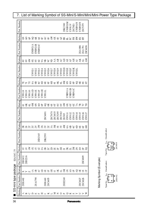
7. List of Marking Symbol of SS-Mini/S-Mini/Mini/Mini-Power Type Package 7. List of Marking Symbol of SS-Mini/S-Mini/Mini/Mini-Power Type Package
2SC5473 3SK269 3SK268 3SK270 3SK271 3SK272 3SK287
37
38
EIAJ:SC–88 8X 8Y 8Z 9E 9U 9V 9W 9Y 9Z AA AO BE BF BH BI BK BL BM BN BO BP EN EO ER EZ FO HC HE HM HO IA IB IS IT OB OE OF OH ON XP4506 XP5555 XP4683 XP5543 XP5A554 XP431N XP05554 XP0D875 XP04286 XP06545 XP06531 XP05534 XP04387 XP4608 XP421F XP4130 XP4402 XP4482 XP6215 XP6216 XP4210 XP7602 XP4111 XP4211 XP7651 XP6543 XP8081 XP6214 XP4509 XP411D XP411E XP411F XP4110 XP4114 XP4117 XP4118 XP4119 XP421D XP421E BR BS BT BU BV BW BX BY BZ CA CB CC CD CE CF CH CI CK CL CM CN XP4214 XP4217 XP4218 XP4219 XP431D XP431E XP431F XP4310 XP4313 XP4314 XP4315 XP4317 XP4318 XP4319 XP611D XP611E XP6110 XP6114 XP6117 XP6118 XP6119 CO CP CQ CR CS CU CV CW CY DF DH DI DK DL DM DN DO DT DZ ED EE XP621D XP621E XP621F XP6210 XP6217 XP6219 XP4404 XP4381 XP6218 XP411H XP411L XP421L XP421K XP611H XP611L XP621L XP621K XP6A554 XP4505 XP4654 XP4314
人类染色体 17p133 位点新克隆基因
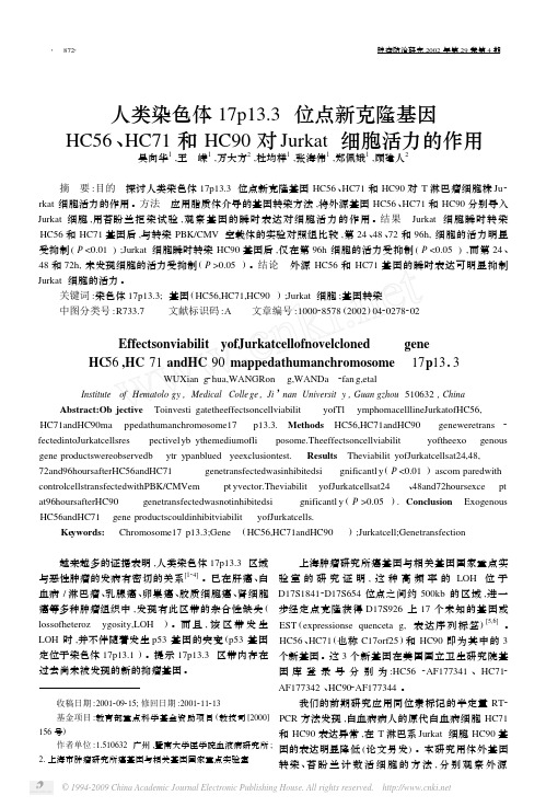
人类染色体17p13.3位点新克隆基因HC56、HC71和HC90对Jurkat 细胞活力的作用吴向华1,王 嵘1,万大方2,杜均样1,张海伟1,郑佩娥1,顾建人2 摘 要:目的 探讨人类染色体17p13.3位点新克隆基因HC56、HC71和HC90对T 淋巴瘤细胞株Ju 2rkat 细胞活力的作用。
方法 应用脂质体介导的基因转染方法,将外源基因HC56、HC71和HC90分别导入Jurkat 细胞,用苔盼兰拒染试验,观察基因的瞬时表达对细胞活力的作用。
结果 Jurkat 细胞瞬时转染HC56和HC71基因后,与转染PBK/CMV 空载体的实验对照组比较,第24、48、72和96h,细胞的活力明显受抑制(P <0.01);Jurkat 细胞瞬时转染HC90基因后,仅在第96h 细胞的活力受抑制(P <0.05),而第24、48和72h,未发现细胞的活力受抑制(P >0.05)。
结论 外源HC56和HC71基因的瞬时表达可明显抑制Jurkat 细胞的活力。
关键词:染色体17p13.3;基因(HC56,HC71,HC90);Jurkat 细胞;基因转染 中图分类号:R733.7 文献标识码:A 文章编号:100028578(2002)0420278202 收稿日期:2001209215;修回日期:2001211213 基金项目:教育部重点科学基金资助项目(教技司[2000]156号) 作者单位:1.510632广州,暨南大学医学院血液病研究所;2.上海市肿瘤研究所癌基因与相关基因国家重点实验室Effectsonviabilit yofJurkatcellofnovelcloned geneHC 56,HC 71andHC 90mappedathumanchromosome 17p 13.3WUXian g 2hua,WANGRong,WANDa 2fan g,etalInstitute of Hematolo gy ,Medical Colle ge ,Ji ’nan Universit y ,Guan gzhou 510632,China Abstract:Ob jective Toinvesti gatetheeffectsoncellviabilit yofTl ymphomacelllineJurkatofHC56,HC71andHC90ma ppedathumanchromosome17p13.3.Methods HC56,HC71andHC90geneweretrans 2fectedintoJurkatcellsres pectivelyb ythemediumofli posome.Theeffectsoncellviabilit yoftheexo genous gene productswereobservedb ytr ypanblued yeexclusiontest.Results Theviabilit yofJurkatcellsat24,48,72and96hoursafterHC56andHC71genetransfectedwasinhibitedsi gnificantl y (P <0.01)ascom paredwith controlcellstransfectedwithPBK/CMVempt yvector.TheviabilityofJurkatcellsat24、48and72hoursexce pt at96hoursafterHC90genetransfectedwasnotinhibitedsi gnificantl y (P >0.05).Conclusion Exogenous HC56andHC71gene productscouldinhibitviabilit yofJurkatcells. Ke ywords: Chromosome17p13.3;Gene (HC56,HC71andHC90);Jurkatcell;Genetransfection 越来越多的证据表明,人类染色体17p13.3区域与恶性肿瘤的发病有密切的关系[124]。
- 1、下载文档前请自行甄别文档内容的完整性,平台不提供额外的编辑、内容补充、找答案等附加服务。
- 2、"仅部分预览"的文档,不可在线预览部分如存在完整性等问题,可反馈申请退款(可完整预览的文档不适用该条件!)。
- 3、如文档侵犯您的权益,请联系客服反馈,我们会尽快为您处理(人工客服工作时间:9:00-18:30)。
OB2216Primary-Side Regulation PWM Power SwitchGENERAL DESCRIPTIONOB2216 is an offline PWM Power switch for low power AC/DC charger and adaptor applications. It operates in primary-side sensing and regulation. Consequently, opto-coupler and TL431 could be eliminated. Proprietary Constant Voltage (CV) and Constant Current (CC) control is integrated as shown in the figure below.In CC control, the current and output power setting can be adjusted externally by the sense resistor Rs at CS pin. In CV control, multi-mode operations are utilized to achieve high performance and high efficiency. Device operates in fixed frequency modeat large load conditions, frequency reduction mode at light/medium load and ‘Extended burst mode’ at No/light load conditions.OB2216 offers power on soft start control and protection coverage with auto-recovery features including Cycle-by-Cycle current limiting, VDD clamp and UVLO. Excellent EMI performance is achieved with On-Bright proprietary frequency shuffling technique together with soft switching control at the totem pole gate drive output.Fig 1. Typical CC/CV CurveFEATURESPrimary-side Sensing and Regulation WithoutTL431 and Opto-couplerMulti-mode Operation for High Efficiency Programmable CV and CC RegulationAdjustable Constant Current and Output PowersettingFrequency Shuffling and Adjustable Gate DriveGreatly Improving EMIPower on Soft-start Time (4ms)“Extended Burst Mode Control” for ImprovedEfficiency and Minimum Standby Design Built-in Leading Edge Blanking (LEB) Cycle-by-Cycle Current LimitingVDD Under Voltage Lockout with Hysteresis(UVLO) VDD ClampAPPLICATIONSLow Power AC/DC offline SMPS forCell Phone ChargerDigital Cameras Charger Small Power AdaptorAuxiliary Power for PC, TV etc. Linear Regulator/RCC ReplacementOB2216 is offered in DIP8 packageTYPICAL APPLICATIONOB2216Primary-Side Regulation PWM Power SwitchGENERAL INFORMATIONPin ConfigurationThe pin map is shown as below for DIP8.Ordering InformationPart Number DescriptionOB2216AP DIP8,Pb-freeAbsolute Maximum RatingsParameter ValueDrain Voltage (off state) -0.3V to BvdssVDD Voltage -0.3 to V DD_clampVDDG Voltage -0.3 to V DD_clampVDD Zener ClampContinuous Current10 mACS Input Voltage -0.3 to 7VINV Input Voltage -0.3 to 7VMin/Max OperatingJunction Temperature T J-20 to 150 oCMin/Max StorageTemperature T stg-55 to 150 o CLead Temperature(Soldering, 10secs)260 o CNote: Stresses beyond those listed under “absolute maximumratings” may cause permanent damage to the device. These arestress ratings only, functional operation of the device at these orany other conditions beyond those indicated under “recommendedoperating conditions” is not implied. Exposure to absolutemaximum-rated conditions for extended periods may affect devicereliability.OB2216Primary-Side Regulation PWM Power SwitchMarking InformationTERMINAL ASSIGNMENTSPin Num Pin Name I/O Description1 VDDG P Internal Gate Driver Power Supply2 VDD P IC DC power supply Input3 INVIInverting input of error amplifier (EA). Connected to resistor divider fromprimary sensing winding reflecting output voltage. PWM duty cycle isdetermined by EA output and current sense signal at pin 4.4 CS I Current sense input5/6 Drain OHV MOSFET Drain Pin. The Drain pin is connected to the primary lead ofthe transformer7/8 GND PGroundOutput Power Table230VAC±15% 85-264VAC ProductOpen Frame1 Open Frame1OB2216 20W 15WNotes:1. Maximum practical continuous power in an open frame design with sufficient drain pattern as a heat sink, at 50℃ ambient.BLOCK DIAGRAMELECTRICAL CHARACTERISTICS(T A = 25O C, VDD=VDDG=16V, if not otherwise noted) Symbol Parameter Test Conditions Min Typ Max Unit Supply Voltage (VDD) SectionI DD ST Standby CurrentVDD=13.5V 5 10uA I DD op Operation Current Operation supply current INV=1.25V, CS=0V, VDD=VDDG=20V - 1.02.0 mA UVLO(ON) VDD Under Voltage Lockout Enter7.5 8.5 9.5VUVLO(OFF)VDD Under Voltage Lockout Exit14.0 15 16.0VV DD _clamp I DD =10mA 38 V Current Sense Input SectionT LEB LEB time540 ns Vth_oc V th _OCtest780 820 860 mV Td_oc Propagation delay 110 ns Z SENSE _IN Input Impedance 50 Kohm T_ss Soft start time4msCV Section Freq Normal mode frequency 45 50 55 KHzFreq_Burst Burst Mode Base Frequency 22KHz△f/Freq Frequency shuffling range+/-4 %CC SectionMinimum frequency 12 KHz Freq Oscillation FrequencyMaximum frequency 50 KHz Error Amplifier section Vref_EA Reference voltage for EA 1.21 1.25 1.29 V Gdc DC gain of the EA 50 dB GBWUnity gain bandwidth37.5kHzPower MOSFET Section BVdssMOSFET Off-state Drain-Source Breakdown600 VRdson Static, Id =0.9A4.45.5 ΏCHARACTERIZATION PLOTSOPERATION DESCRIPTIONOB2216 is cost effective PWM power switch optimized for off-line low power AC/DC applications including battery chargers and adaptors. It operates in primary side sensing and regulation, thus opto-coupler and TL431 are not required. Proprietary CC control and built-in error amplifier can achieve a good CC/CV performance.z Startup Current and Start up Control Startup current of OB2216 is designed to be very low so that VDD could be charged up above UVLO threshold and starts up quickly. A large value startup resistor can therefore be used to minimize the power loss in application.z Operating CurrentThe Operating current of OB2216 is as low as 1mA. Good efficiency is achieved with the low operating current together with ‘Extended burst mode’ control features.z Soft StartOB2216 features an internal 4ms soft start to minimize the component electrical over-stress during power on startup. As soon as VDD reaches UVLO(OFF), the control algorithm will ramp peak current voltage threshold gradually from nearly zero to normal setting of 0.82V. Every restart is a soft start.z CC/CV OperationOB2216 is designed to produce good CC/CV control characteristic as shown in the Fig. 1.In charger applications, a discharged battery charging starts in the CC portion of the curve until it is nearly full charged and smoothly switches to operate in CV portion of the curve.In an AC/DC adapter, the normal operation occurs only on the CV portion of the curve. The CC portion provides output current limiting. In CV operation, the output voltage is regulated through the primary side control.To support OB2216 proprietary CC/CV control, system needs to be designed in DCM mode for flyback system. Under normal operation, when INV is less than Vref, the system works in CC control, Otherwise, the system works in CV control.z Error Amplifier (EA)Connected to a resistor divider from the primary side sensing winding, the inverting input of the Error Amplifier (EA) is compared to an internal reference voltage of 1.25V to regulate the output voltage. The EA output is internally connected to the PWM generator and controls the duty cycle.z Adjustable CC point and Output PowerIn OB2216, the CC point and output power can be externally adjusted by external current sense resistor Rs at CS pin. The output power is adjusted through CC point change. The larger Rs, the smaller CC point is, and the smalleroutput power becomes, and vice versa as shown in Fig.2.Fig. 2 Adjustable output power by changing Rsz Extended Burst Mode OperationAt light load or zero load condition, most of the power dissipation in a switching mode power supply is from switching loss, the core loss of the transformer and the loss on the snubber circuit. The magnitude of power loss is in proportion to the switching frequency. Lower switching frequency leads to the reduction on the power loss and thus conserves the energy.OB2216 self adjusts the switching frequency according to the loading condition. The switch frequency is reduced at light/no load condition to improve the conversion efficiency. At light load/no load condition, the output of the Error amplifier (EA) drops below the burst mode threshold level and device enters Burst Mode control. The frequency control also eliminates the audio noise at any loading conditions.z Operation switching frequencyThe switching frequency of OB2216 is adaptively controlled according to CC/CV operation. No external frequency setting components are required.z Frequency shuffling for EMI improvement The frequency Shuffling (switching frequency modulation) is implemented in OB2216. The oscillation frequency is modulated so that the tone energy is spread out. The spread spectrum minimizes the conduction band EMI and therefore eases the system design.z Current Sensing and Leading Edge Blanking Cycle-by-Cycle current limiting is offered in OB2216 current mode PWM control. The switch current is detected by a sense resistor into the CS pin. An internal leading edge blanking circuit chops off the sensed voltage spike at initial internal power MOSFET on state so that the external RC filtering on sense input is no longer needed. The PWM duty cycle is determined by the current sense input voltage and the EA output voltage. z Adjustable Drive CapabilityThe internal power MOSFET in OB2216 is driven by a dedicated gate driver for power switch control. Too weak the gate drive strength results in higher conduction and switch loss of MOSFET while too strong gate drive compromises EMI.A good tradeoff is achieved through the built-in totem pole gate design with right output strength control. The gate drive strength can be adjusted externally by a resistor connected between VDD and VDDG. The low idle loss and good EMI system design is possible with this dedicated control scheme. z Protection ControlGood power supply system reliability is achieved with its rich protection features including Cycle-by-Cycle current limiting (OCP), VDD protection and clamp, Power on Soft Start, and Under Voltage Lockout on VDD (UVLO).VDD is supplied by transformer auxiliary winding output. The output of OB2216 is shut down when VDD drops below UVLO(ON) limit and Switcher enters power on start-up sequence thereafter.。