41SM30-H58;中文规格书,Datasheet资料
SPU0410HR5H-PB, 规格书,Datasheet 资料
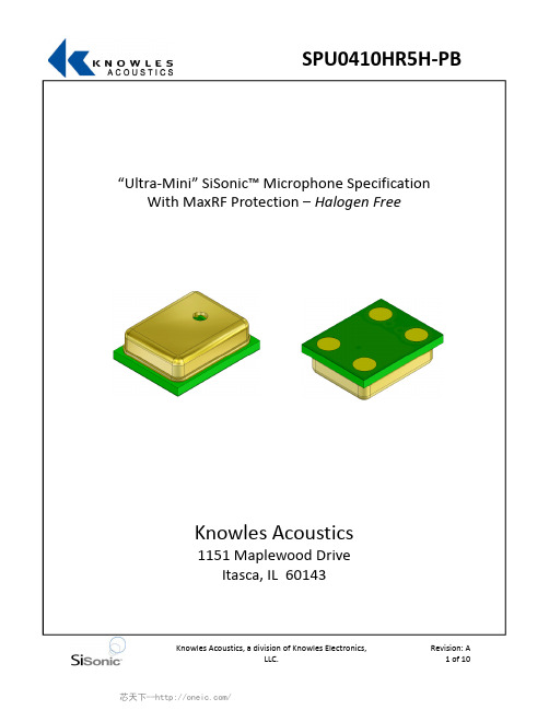
“Ultra‐Mini” SiSonic™ Microphone Specification With MaxRF Protection –Halogen FreeKnowles Acoustics1151 Maplewood DriveItasca, IL 601431. DESCRIPTION AND APPLICATION1.1 Description“Ultra Mini” Surface Mount Silicon Microphone with Maximum RF Protection –Halogen Free 1.2 ApplicationHand held consumer electronics2. PART MARKINGIdentification Number ConventionS 1 2 34 5 6 7S: Manufacturing Location“S” –Knowles Electronics SuzhouSuzhou, China“No Alpha Character” –Knowles Electronics ItascaItasca, IL USA 3“E” –Engineering Samples Digits 1 –7: Job Identification Number3.TEMPERATURE RANGE 3.1 Operating Temperature Range: ‐40°C to +100°C 3.2 Storage Temperature Range: ‐40°C to +100°C4. ACOUSTIC & ELECTRICAL SPECIFICATIONSSymbol ConditionLimitsUnit Min.Nom.Max.Directivity Omni‐directionalSensitivity S@ 1kHz (0dB=1V/Pa)‐45‐42‐39dB Output impedance Z OUT@ 1kHz (0dB=1V/Pa)‐‐‐‐‐‐300ΩCurrent Consumption I DSS across 1.5 to 3.6 volts‐‐‐‐‐‐250μA Signal to Noise Ratio S/N@ 1kHz (0dB=1V/Pa)‐‐‐59‐‐‐dB Supply Voltage Vs 1.5‐‐‐ 3.6VSensitivity Loss acrossVoltage Change in sensitivity over3.6v to 1.5vNo Change Across VoltageRangedBTHD At 100dB SPL, THD < 1%At 115dB SPL, THD < 10%dB5. FREQUENCY RESPONSE CURVE66. MECHANICAL SPECIFICATIONS7. RECOMMENDED CUSTOMER7LAND PATTERN8. RECOMMENDED SOLDER STENCIL PATTERNN/A9. RECOMMENDED INTERFACE CIRCUIT10. DETAIL 10PACKAGING11. SOLDER REFLOW PROFILE170–180°CSolder Melt Pre ‐heat 260°C230°Csec sec Stage Temperature ProfileTime (maximum)Pre ‐heat 170 ~ 180 C 120 sec.Solder Melt Above 230 C 100 sec.100 sec.120 sec.Notes:1.Do not pull a vacuum over the port hole of the microphone. Pulling avacuum over the port hole can damage the device.the reflow process.Board washing and cleaning Peak260 C maximum30 sec.2.Do not board wash afteragents can damage the device. Do not expose to ultrasonic processing or cleaning.3.Number of Reflow = recommend no more than 3 cycles.12ADDITIONAL NOTES (A)Shelf life: Twelve (12) months when devices are to be stored in factory supplied, unopened ESD moisture sensitive bag under maximum environmental conditions of 30ºC, 70% R.H. (B)MSL (moisture sensitivity level) Class 2a.12.13. RELIABILITY SPECIFICATIONSNote: After test conditions are performed, the sensitivity of the microphone shall not deviate more than 3dB from its initial value.Test DescriptionThermal Shock100 cycles of air‐air thermal shock from ‐40C to +125Cwith 15min soaks. (ICE 68‐2‐4)High Temperature St +105C environment for 1,000 hours. (IEC 68‐2‐2 Test Ba)StorageLow TemperatureStorage‐40C environment for 1,000 hours. (IEC 68‐2‐2 Test Aa)High Temperature Bias+105C environment while under bias for 1,000 hours. (IEC68‐2‐2 Test Ba)Low Temperature Bias‐40C environment while under bias for 1,000 hours. (IEC68‐2‐2 Test Aa)Temperature / Humidity Bias +85C/85% RH environment while under bias for 500 hours. (JESD22‐A101A‐B)Vibration4 cycles lasting 12 minutes from 20 to 2,000Hz in X, Y, andZ direction with a peak acceleration of 20g. (MIL 883E,Method 2007.2, A)Electrostatic Discharge3 discharges at +/‐8kV direct contact to the lid when unitis grounded (IEC 61000‐4‐2) and 3 discharges at +/‐2kVdirect contact to the I/O pins (MIL 883E, Method 3015.7) Reflow5 reflow cycles with peak temperature of 260C. Mechanical Shock3 pulses of 10,000g in the X, Y, and Z direction. (IEC 68‐2‐27, Test Ea)14. SPECIFICATION REVISIONSRevision Detailed Specification Changes Date X1Preliminary Specification Release06‐24‐2008A Specification 02172009release‐‐The information contained in this literature is based on our experience to date and is believed to be reliable and it is subject to change without notice.It is intended as a guide for use by persons having technical skill at their own discretion and risk.We do not guarantee favorable results or assume any liability in connection with its use.Dimensions contained herein are for reference purposes only.For specific dimensional requirements consult factory.This publication is not to be taken as a license to operate under,or recommendation to infringe any existing patents.This supersedes and voids all previous literature.。
74271112S;中文规格书,Datasheet资料
7.1 7.0 6.02012-06-272012-04-302008-01-03SStSStSMuSStSMu-Würth Elektronik eiSos GmbH & Co. KGEMC & Inductive SolutionsMax-Eyth-Str. 174638 WaldenburgGermanyTel. +49 (0) 79 42 945 - 0A Dimensions: [mm] Additional FeaturesSafety key to lock/ unkock STAR-CLIP Fixation74271 7427711D2 General Properties:Ferrite core Ferrite core Ferrite core Plastic housing Plastic housing Test cable Test cablePropertiesMaterial Initial permeability Curie temperatureColourFlammability ClassificationApplicable cable Applicable cable lengthµi T CValue 4 W 620620150Black UL94-V0AWG2690Unit°Cmm Tol.typ.typ.F Typical Impedance Characteristics:I Cautions and Warnings:The following conditions apply to all goods within the product series of WE-STAR TECof Würth Elektronik eiSos GmbH & Co. KG:General:All recommendations according to the general technical specifications of the data sheet have to be complied with.The disposal and operation of the product within ambient conditions which probably alloy or harm the component surface has to be avoided.The packaging of the product is to encase the needed humidity of the plastic housing. To ensure the humidity level, the products have to be stored in this delivered packaging. If not, the products are losing their humidity. In this case you can re-condition the components according to the internal standard WE1883 to ensure the necessary humidity in the plastic.To ensure the operating mode of the product, the ambient temperature at processing (when the part will be mounted on the cable) has to be in the range of 15 to 25 °C.Before mounting, the part should be stored for one hour in this condition.The responsibility for the applicability of customer specific products and the use in a particular customer design is always within the authority of the customer. All technical specifications for standard products do also apply for customer specific products.Direct mechanical impact to the product and the forcible closing of this shall be prevented as the ferrite material of the ferrite body or the pla-stic housing could flake or in the worst case it could break.Product specific:Follow all instructions mentioned in the datasheet, especially:•The cable diameter must be pointed out, otherwise no warranty will be sustained.•Violation of the technical product specifications such as exceeding the nominal rated current will result in the loss of warranty.1. General Customer ResponsibilitySome goods within the product range of Würth Elektronik eiSos GmbH & Co. KG contain statements regarding general suitability for certain application areas. These statements about suitability are based on our knowledge and experience of typical requirements concerning the are-as, serve as general guidance and cannot be estimated as binding statements about the suitability for a customer application. The responsibi-lity for the applicability and use in a particular customer design is always solely within the authority of the customer. Due to this fact it is up to the customer to evaluate, where appropriate to investigate and decide whether the device with the specific product characteristics described in the product specification is valid and suitable for the respective customer application or not.2. Customer Responsibility related to Specific, in particular Safety-Relevant ApplicationsIt has to be clearly pointed out that the possibility of a malfunction of electronic components or failure before the end of the usual lifetime can-not be completely eliminated in the current state of the art, even if the products are operated within the range of the specifications.In certain customer applications requiring a very high level of safety and especially in customer applications in which the malfunction or failure of an electronic component could endanger human life or health it must be ensured by most advanced technological aid of suitable design of the customer application that no injury or damage is caused to third parties in the event of malfunction or failure of an electronic component.3. Best Care and AttentionAny product-specific notes, warnings and cautions must be strictly observed.4. Customer Support for Product SpecificationsSome products within the product range may contain substances which are subject to restrictions in certain jurisdictions in order to serve spe-cific technical requirements. Necessary information is available on request. In this case the field sales engineer or the internal sales person in charge should be contacted who will be happy to support in this matter.5. Product R&DDue to constant product improvement product specifications may change from time to time. As a standard reporting procedure of the Product Change Notification (PCN) according to the JEDEC-Standard inform about minor and major changes. In case of further queries regarding the PCN, the field sales engineer or the internal sales person in charge should be contacted. The basic responsibility of the customer as per Secti-on 1 and 2 remains unaffected.6. Product Life CycleDue to technical progress and economical evaluation we also reserve the right to discontinue production and delivery of products. As a stan-dard reporting procedure of the Product Termination Notification (PTN) according to the JEDEC-Standard we will inform at an early stage about inevitable product discontinuance. According to this we cannot guarantee that all products within our product range will always be available. Therefore it needs to be verified with the field sales engineer or the internal sales person in charge about the current product availability ex-pectancy before or when the product for application design-in disposal is considered.The approach named above does not apply in the case of individual agreements deviating from the foregoing for customer-specific products.7. Property RightsAll the rights for contractual products produced by Würth Elektronik eiSos GmbH & Co. KG on the basis of ideas, development contracts as well as models or templates that are subject to copyright, patent or commercial protection supplied to the customer will remain with Würth Elektronik eiSos GmbH & Co. KG.8. General Terms and ConditionsUnless otherwise agreed in individual contracts, all orders are subject to the current version of the “General Terms and Conditions of Würth Elektronik eiSos Group”, last version available at .J Important Notes:The following conditions apply to all goods within the product range of Würth Elektronik eiSos GmbH & Co. KG:分销商库存信息: WURTH-ELECTRONICS 74271112S。
RB520S30;中文规格书,Datasheet资料
RB520S30 — Schottky Barrier Diodes
Physical Dimension
SOD-523F
© 2009 Fairchild Semiconductor Corporation
RB520S30 Rev. A2
4
/
Units
VRRM
Maximum Repetitive Reverse Voltage
30
V
IF(AV)
Average Rectified Forward Current
200
mA
TJ
Operating Junction Temperature Range
-55 to +125
°C
TSTG
Storage Temperature Range
Electrical Characteristics TA=25°C unless otherwise noted
Symbol
Parameter
Test Condition
BVR Breakdown Voltage IR Reverse Leakage Current VF Forward Voltage
• Green Mold Compound
SOD-523F Band Indicates Cathode RB520S30 Marking : 1B
Absolute Maximum Ratings * TA=25°C unless otherwise noted
Symbol
Parameter
Value
Parameter
PD RθJA
Total Device Dissipation (TC=25°C) Thermal Resistance, Junction to Ambient
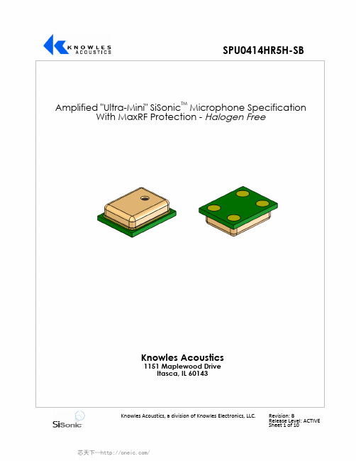
SPU0414HR5H-SB, 规格书,Datasheet 资料
3. TEMPERATURE RANGE
3.1 Operating Temperature Range: -40 C to +100 C 3.2 Storage Temperature Range: -40 C to +100 C
Knowles Acoustics, a division of Knowles Electronics, LLC.
Identification Number Convention S 4 1 5 2 6 3 7
S: Manufacturing Location "S" - Knowles Electronics Suzhou Suzhou, China "No Alpha Character" - Knowles Electronics Itasca, IL USA "E" - Engineering Samples Digits 1-7: Job Identification Number
Date
4-23-2009 10-21-2010
The information contained in this literature is based on our experience to date and is believed to be reliable and it is subject to change without notice. It is intended as a guide for use by persons having technical skill at their own discretion and risk. We do not guarantee favorable results or assume any liability in connection with its use. Dimensions contained herein are for reference purposes only. For specific dimensional requirements consult factory. This publication is not to be taken as a license to operate under, or recommendation to infringe any existing patents. This supersedes and voids all previous literature.
BSS84AKS,115;中文规格书,Datasheet资料
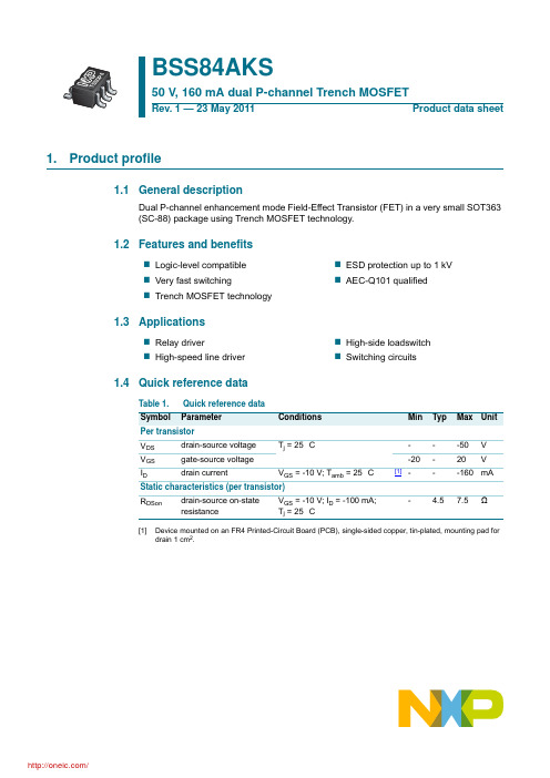
1.Product profile1.1General descriptionDual P-channel enhancement mode Field-Effect Transistor (FET) in a very small SOT363 (SC-88) package using Trench MOSFET technology.1.2Features and benefitsLogic-level compatible Very fast switchingTrench MOSFET technologyESD protection up to 1 kV AEC-Q101 qualified1.3ApplicationsRelay driverHigh-speed line driverHigh-side loadswitch Switching circuits1.4Quick reference data[1]Device mounted on an FR4 Printed-Circuit Board (PCB), single-sided copper, tin-plated, mounting pad for drain 1 cm 2.BSS84AKS50 V, 160 mA dual P-channel Trench MOSFETRev. 1 — 23 May 2011Product data sheetTable 1.Quick reference data Symbol ParameterConditions Min Typ Max Unit Per transistorV DS drain-source voltage T j =25°C---50V V GS gate-source voltage -20-20VI D drain currentV GS =-10V;T amb =25°C [1]---160mA Static characteristics (per transistor)R DSondrain-source on-state resistanceV GS =-10V;I D =-100mA; T j =25°C-4.57.5Ω2.Pinning information3.Ordering information4.Marking[1]% = placeholder for manufacturing site codeTable 2.Pinning information Pin Symbol Description Simplified outline Graphic symbol1S1source 1SOT363 (TSSOP6)2G1gate 13D2drain 24S2source 25G2gate 26D1drain 1132456sym147G1G2Table 3.Ordering informationType numberPackage NameDescriptionVersion BSS84AKSTSSOP6plastic surface-mounted package; 6 leadsSOT363Table 4.Marking codesType number Marking code [1]BSS84AKS%VY5.Limiting valuesTable 5.Limiting valuesIn accordance with the Absolute Maximum Rating System (IEC 60134).Symbol Parameter Conditions Min Max Unit Per transistorV DS drain-source voltage T j=25°C--50VV GS gate-source voltage-2020VI D drain current V GS=-10V; T amb=25°C[1]--160mAV GS=-10V; T amb=100°C[1]--100mA I DM peak drain current T amb=25°C; single pulse; t p≤10µs--640mA P tot total power dissipation T amb=25°C[2]-280mW[1]-320mWT sp=25°C-990mW Per deviceP tot total power dissipation T amb=25°C[2]-445mW T j junction temperature-55150°C T amb ambient temperature-55150°C T stg storage temperature-65150°C Source-drain diodeI S source current T amb=25°C[1]--160mA ESD maximum ratingV ESD electrostatic discharge voltage HBM[3]-1000V[1]Device mounted on an FR4 Printed-Circuit Board (PCB), single-sided copper, tin-plated, mounting pad for drain 1 cm2.[2]Device mounted on an FR4 Printed-Circuit Board (PCB), single-sided copper, tin-plated and standard footprint.[3]Measured between all pins.6.Thermal characteristicsTable 6.Thermal characteristicsSymbol Parameter Conditions Min Typ Max Unit Per deviceR th(j-a)thermal resistance from junction to ambient in free air[1]--300K/W Per transistorR th(j-a)thermal resistance from junction to ambient in free air[1]-390445K/W[2]-340390K/W R th(j-sp)thermal resistance from junction to solder point--130K/W[1]Device mounted on an FR4 PCB, single-sided copper, tin-plated and standard footprint.[2]Device mounted on an FR4 Printed-Circuit Board (PCB), single-sided copper, tin-plated, mounting pad for drain 1 cm2.7.CharacteristicsTable 7.CharacteristicsSymbol Parameter Conditions Min Typ Max Unit Static characteristics (per transistor)V(BR)DSS drain-source breakdownvoltageI D=-10µA; V GS=0V;T j=25°C-50--VV GSth gate-source thresholdvoltageI D=-250µA; V DS=V GS; T j=25°C-1.1-1.6-2.1VI DSS drain leakage current V DS=-50V; V GS=0V; T j=25°C---1µAV DS=-50V; V GS=0V; T j=150°C---2µA I GSS gate leakage current V GS=-20V;V DS=0V; T j=25°C---10µAV GS=20V;V DS=0V; T j=25°C---10µAR DSon drain-source on-stateresistance V GS=-10V;I D=-100mA; T j=25°C- 4.57.5ΩV GS=-10V;I D=-100mA; T j=150°C-813.5ΩV GS=-5V; I D=-100mA; T j=25°C- 5.78.5Ωg fs forward transconductance V DS=-10V; I D=-100mA; T j=25°C-150-mS Dynamic characteristics (per transistor)Q G(tot)total gate charge V DS=-25V; I D=-200mA; V GS=-5V;T j=25°C -0.260.35nCQ GS gate-source charge-0.12-nC Q GD gate-drain charge-0.09-nCC iss input capacitance V DS=-25V; f=1MHz; V GS=0V;T j=25°C -2436pFC oss output capacitance- 4.5-pF C rss reverse transfercapacitance- 1.3-pFt d(on)turn-on delay time V DS=-30V; R L=250Ω; V GS=-10V;R G(ext)=6Ω; T j=25°C -1326nst r rise time-11-ns t d(off)turn-off delay time-4896ns t f fall time-25-ns Source-drain diode (per transistor)V SD source-drain voltage I S=-115mA; V GS=0V; T j=25°C-0.48-0.85-1.2V分销商库存信息: NXPBSS84AKS,115。
Ra-01S规格书说明书
Ra-01S规格书版本V1.1版权©2020免责申明和版权公告本文中的信息,包括供参考的URL地址,如有变更,恕不另行通知。
文档“按现状”提供,不负任何担保责任,包括对适销性、适用于特定用途或非侵权性的任何担保,和任何提案、规格或样品在他处提到的任何担保。
本文档不负任何责任,包括使用本文档内信息产生的侵犯任何专利权行为的责任。
本文档在此未以禁止反言或其他方式授予任何知识产权使用许可,不管是明示许可还是暗示许可。
文中所得测试数据均为安信可实验室测试所得,实际结果可能略有差异。
文中提到的所有商标名称、商标和注册商标均属其各自所有者的财产,特此声明。
最终解释权归深圳市安信可科技有限公司所有。
注意由于产品版本升级或其他原因,本手册内容有可能变更。
深圳市安信可科技有限公司保留在没有任何通知或者提示的情况下对本手册的内容进行修改的权利。
本手册仅作为使用指导,深圳市安信可科技有限公司尽全力在本手册中提供准确的信息,但是深圳市安信可科技有限公司并不确保手册内容完全没有错误,本手册中的所有陈述、信息和建议也不构成任何明示或暗示的担保。
文件制定/修订/废止履历表版本日期制定/修订内容制定核准V1.02020.8.12首版徐V1.12020.8.19更新部分参数徐目录一、产品概述 (5)二、电气参数 (6)三、外观尺寸 (8)四、管脚定义 (10)五、原理图 (11)六、设计指导 (12)七、回流焊曲线图 (14)八、包装信息 (15)九、联系我们 (15)一、产品概述安信可LoRa系列模块(Ra-01S)由安信可科技设计开发。
该模组用于超长距离扩频通信,其射频芯片SX1268主要采用LoRa™远程调制解调器,用于超长距离扩频通信,抗干扰性强,能够最大限度降低电流消耗。
借助SEMTECH的LoRa™专利调制技术,SX1268具有超过-148dBm的高灵敏度,+22dBm的功率输出,传输距离远,可靠性高。
同时,相对传统调制技术,LoRa™调制技术在抗阻塞和选择方面也具有明显优势,解决了传统设计方案无法同时兼顾距离、抗干扰和功耗的问题。
DSEI60-06A;中文规格书,Datasheet资料

166 W
0.8...1.2 Nm
6
g
Symbol
IR
VF
VT0 rT RthJC RthCH trr IRM
Conditions
Characteristic Values typ. max.
VR = VRRM VR = 0.8·VRRM VR = 0.8·VRRM
TVJ = 25°C TVJ = 25°C TVJ = 125°C
IXYS reserves the right to change limits, test conditions and dimensions
© 2007 IXYS All rights reserved
/
0549
2-2
Dimensions TO-247 AD
C
D
t = 8.3 ms (60 Hz), sine
TC = 25°C mounting torque typical
Maximum Ratings
100 A 60 A
550 A 600
480 A 520Biblioteka 1510 A2s 1490
1150 A2s 1120
-55...+150 °C 150 °C
-55...+150 °C
Fast Recovery Epitaxial Diode (FRED)
DSEI60-06A DSEI60-06AT
IFAV = 60 A VRRM = 600 V trr = 35 ms
VRSM V
600 600
VRRM V
600 600
Type
DSEI 60-06A DSEI 60-06AT
A
SGH30N60RUFDTU;中文规格书,Datasheet资料
-- 1733 2430 uJ
--
34
--
ns
--
67
--
ns
--
60
90
ns
--
281 400
ns
--
921
--
uJ
-- 1556 --
uJ
-- 2477 3470 uJ
10
--
--
us
--
85 120 nC
--
17
25
nC
--
39
55
nC
--
14
--
nH
Electrical Characteristics of DIODE TC = 25°C unless otherwise noted
E
SGH30N60RUFD 600 ± 20 48 30 90 25 220 10 235 90
-55 to +150 -55 to +150
300
Typ. ----
Max. 0.53 0.83 40
Units V V A A A A A us W W °C °C °C
Units °C/W °C/W °C/W
Symbol VCES VGES
IC
ICM (1) IF IFM TSC PD
TJ Tstg
TL
Description
Collector-Emitter Voltage
Gate-Emitter Voltage
Collector Current Collector Current Pulsed Collector Current
Thermal Characteristics