M38124M4-XXXSP中文资料
Native Instruments MASCHINE MK3 用户手册说明书
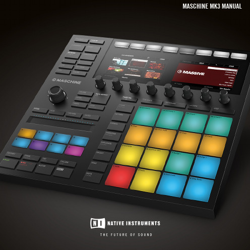
The information in this document is subject to change without notice and does not represent a commitment on the part of Native Instruments GmbH. The software described by this docu-ment is subject to a License Agreement and may not be copied to other media. No part of this publication may be copied, reproduced or otherwise transmitted or recorded, for any purpose, without prior written permission by Native Instruments GmbH, hereinafter referred to as Native Instruments.“Native Instruments”, “NI” and associated logos are (registered) trademarks of Native Instru-ments GmbH.ASIO, VST, HALion and Cubase are registered trademarks of Steinberg Media Technologies GmbH.All other product and company names are trademarks™ or registered® trademarks of their re-spective holders. Use of them does not imply any affiliation with or endorsement by them.Document authored by: David Gover and Nico Sidi.Software version: 2.8 (02/2019)Hardware version: MASCHINE MK3Special thanks to the Beta Test Team, who were invaluable not just in tracking down bugs, but in making this a better product.NATIVE INSTRUMENTS GmbH Schlesische Str. 29-30D-10997 Berlin Germanywww.native-instruments.de NATIVE INSTRUMENTS North America, Inc. 6725 Sunset Boulevard5th FloorLos Angeles, CA 90028USANATIVE INSTRUMENTS K.K.YO Building 3FJingumae 6-7-15, Shibuya-ku, Tokyo 150-0001Japanwww.native-instruments.co.jp NATIVE INSTRUMENTS UK Limited 18 Phipp StreetLondon EC2A 4NUUKNATIVE INSTRUMENTS FRANCE SARL 113 Rue Saint-Maur75011 ParisFrance SHENZHEN NATIVE INSTRUMENTS COMPANY Limited 5F, Shenzhen Zimao Center111 Taizi Road, Nanshan District, Shenzhen, GuangdongChina© NATIVE INSTRUMENTS GmbH, 2019. All rights reserved.Table of Contents1Welcome to MASCHINE (25)1.1MASCHINE Documentation (26)1.2Document Conventions (27)1.3New Features in MASCHINE 2.8 (29)1.4New Features in MASCHINE 2.7.10 (31)1.5New Features in MASCHINE 2.7.8 (31)1.6New Features in MASCHINE 2.7.7 (32)1.7New Features in MASCHINE 2.7.4 (33)1.8New Features in MASCHINE 2.7.3 (36)2Quick Reference (38)2.1Using Your Controller (38)2.1.1Controller Modes and Mode Pinning (38)2.1.2Controlling the Software Views from Your Controller (40)2.2MASCHINE Project Overview (43)2.2.1Sound Content (44)2.2.2Arrangement (45)2.3MASCHINE Hardware Overview (48)2.3.1MASCHINE Hardware Overview (48)2.3.1.1Control Section (50)2.3.1.2Edit Section (53)2.3.1.3Performance Section (54)2.3.1.4Group Section (56)2.3.1.5Transport Section (56)2.3.1.6Pad Section (58)2.3.1.7Rear Panel (63)2.4MASCHINE Software Overview (65)2.4.1Header (66)2.4.2Browser (68)2.4.3Arranger (70)2.4.4Control Area (73)2.4.5Pattern Editor (74)3Basic Concepts (76)3.1Important Names and Concepts (76)3.2Adjusting the MASCHINE User Interface (79)3.2.1Adjusting the Size of the Interface (79)3.2.2Switching between Ideas View and Song View (80)3.2.3Showing/Hiding the Browser (81)3.2.4Showing/Hiding the Control Lane (81)3.3Common Operations (82)3.3.1Using the 4-Directional Push Encoder (82)3.3.2Pinning a Mode on the Controller (83)3.3.3Adjusting Volume, Swing, and Tempo (84)3.3.4Undo/Redo (87)3.3.5List Overlay for Selectors (89)3.3.6Zoom and Scroll Overlays (90)3.3.7Focusing on a Group or a Sound (91)3.3.8Switching Between the Master, Group, and Sound Level (96)3.3.9Navigating Channel Properties, Plug-ins, and Parameter Pages in the Control Area.973.3.9.1Extended Navigate Mode on Your Controller (102)3.3.10Navigating the Software Using the Controller (105)3.3.11Using Two or More Hardware Controllers (106)3.3.12Touch Auto-Write Option (108)3.4Native Kontrol Standard (110)3.5Stand-Alone and Plug-in Mode (111)3.5.1Differences between Stand-Alone and Plug-in Mode (112)3.5.2Switching Instances (113)3.5.3Controlling Various Instances with Different Controllers (114)3.6Host Integration (114)3.6.1Setting up Host Integration (115)3.6.1.1Setting up Ableton Live (macOS) (115)3.6.1.2Setting up Ableton Live (Windows) (116)3.6.1.3Setting up Apple Logic Pro X (116)3.6.2Integration with Ableton Live (117)3.6.3Integration with Apple Logic Pro X (119)3.7Preferences (120)3.7.1Preferences – General Page (121)3.7.2Preferences – Audio Page (126)3.7.3Preferences – MIDI Page (130)3.7.4Preferences – Default Page (133)3.7.5Preferences – Library Page (137)3.7.6Preferences – Plug-ins Page (145)3.7.7Preferences – Hardware Page (150)3.7.8Preferences – Colors Page (154)3.8Integrating MASCHINE into a MIDI Setup (156)3.8.1Connecting External MIDI Equipment (156)3.8.2Sync to External MIDI Clock (157)3.8.3Send MIDI Clock (158)3.9Syncing MASCHINE using Ableton Link (159)3.9.1Connecting to a Network (159)3.9.2Joining and Leaving a Link Session (159)3.10Using a Pedal with the MASCHINE Controller (160)3.11File Management on the MASCHINE Controller (161)4Browser (163)4.1Browser Basics (163)4.1.1The MASCHINE Library (163)4.1.2Browsing the Library vs. Browsing Your Hard Disks (164)4.2Searching and Loading Files from the Library (165)4.2.1Overview of the Library Pane (165)4.2.2Selecting or Loading a Product and Selecting a Bank from the Browser (170)4.2.2.1[MK3] Browsing by Product Category Using the Controller (174)4.2.2.2[MK3] Browsing by Product Vendor Using the Controller (174)4.2.3Selecting a Product Category, a Product, a Bank, and a Sub-Bank (175)4.2.3.1Selecting a Product Category, a Product, a Bank, and a Sub-Bank on theController (179)4.2.4Selecting a File Type (180)4.2.5Choosing Between Factory and User Content (181)4.2.6Selecting Type and Character Tags (182)4.2.7List and Tag Overlays in the Browser (186)4.2.8Performing a Text Search (188)4.2.9Loading a File from the Result List (188)4.3Additional Browsing Tools (193)4.3.1Loading the Selected Files Automatically (193)4.3.2Auditioning Instrument Presets (195)4.3.3Auditioning Samples (196)4.3.4Loading Groups with Patterns (197)4.3.5Loading Groups with Routing (198)4.3.6Displaying File Information (198)4.4Using Favorites in the Browser (199)4.5Editing the Files’ Tags and Properties (203)4.5.1Attribute Editor Basics (203)4.5.2The Bank Page (205)4.5.3The Types and Characters Pages (205)4.5.4The Properties Page (208)4.6Loading and Importing Files from Your File System (209)4.6.1Overview of the FILES Pane (209)4.6.2Using Favorites (211)4.6.3Using the Location Bar (212)4.6.4Navigating to Recent Locations (213)4.6.5Using the Result List (214)4.6.6Importing Files to the MASCHINE Library (217)4.7Locating Missing Samples (219)4.8Using Quick Browse (221)5Managing Sounds, Groups, and Your Project (225)5.1Overview of the Sounds, Groups, and Master (225)5.1.1The Sound, Group, and Master Channels (226)5.1.2Similarities and Differences in Handling Sounds and Groups (227)5.1.3Selecting Multiple Sounds or Groups (228)5.2Managing Sounds (233)5.2.1Loading Sounds (235)5.2.2Pre-listening to Sounds (236)5.2.3Renaming Sound Slots (237)5.2.4Changing the Sound’s Color (237)5.2.5Saving Sounds (239)5.2.6Copying and Pasting Sounds (241)5.2.7Moving Sounds (244)5.2.8Resetting Sound Slots (245)5.3Managing Groups (247)5.3.1Creating Groups (248)5.3.2Loading Groups (249)5.3.3Renaming Groups (251)5.3.4Changing the Group’s Color (251)5.3.5Saving Groups (253)5.3.6Copying and Pasting Groups (255)5.3.7Reordering Groups (258)5.3.8Deleting Groups (259)5.4Exporting MASCHINE Objects and Audio (260)5.4.1Saving a Group with its Samples (261)5.4.2Saving a Project with its Samples (262)5.4.3Exporting Audio (264)5.5Importing Third-Party File Formats (270)5.5.1Loading REX Files into Sound Slots (270)5.5.2Importing MPC Programs to Groups (271)6Playing on the Controller (275)6.1Adjusting the Pads (275)6.1.1The Pad View in the Software (275)6.1.2Choosing a Pad Input Mode (277)6.1.3Adjusting the Base Key (280)6.1.4Using Choke Groups (282)6.1.5Using Link Groups (284)6.2Adjusting the Key, Choke, and Link Parameters for Multiple Sounds (286)6.3Playing Tools (287)6.3.1Mute and Solo (288)6.3.2Choke All Notes (292)6.3.3Groove (293)6.3.4Level, Tempo, Tune, and Groove Shortcuts on Your Controller (295)6.3.5Tap Tempo (299)6.4Performance Features (300)6.4.1Overview of the Perform Features (300)6.4.2Selecting a Scale and Creating Chords (303)6.4.3Scale and Chord Parameters (303)6.4.4Creating Arpeggios and Repeated Notes (316)6.4.5Swing on Note Repeat / Arp Output (321)6.5Using Lock Snapshots (322)6.5.1Creating a Lock Snapshot (322)6.5.2Using Extended Lock (323)6.5.3Updating a Lock Snapshot (323)6.5.4Recalling a Lock Snapshot (324)6.5.5Morphing Between Lock Snapshots (324)6.5.6Deleting a Lock Snapshot (325)6.5.7Triggering Lock Snapshots via MIDI (326)6.6Using the Smart Strip (327)6.6.1Pitch Mode (328)6.6.2Modulation Mode (328)6.6.3Perform Mode (328)6.6.4Notes Mode (329)7Working with Plug-ins (330)7.1Plug-in Overview (330)7.1.1Plug-in Basics (330)7.1.2First Plug-in Slot of Sounds: Choosing the Sound’s Role (334)7.1.3Loading, Removing, and Replacing a Plug-in (335)7.1.3.1Browser Plug-in Slot Selection (341)7.1.4Adjusting the Plug-in Parameters (344)7.1.5Bypassing Plug-in Slots (344)7.1.6Using Side-Chain (346)7.1.7Moving Plug-ins (346)7.1.8Alternative: the Plug-in Strip (348)7.1.9Saving and Recalling Plug-in Presets (348)7.1.9.1Saving Plug-in Presets (349)7.1.9.2Recalling Plug-in Presets (350)7.1.9.3Removing a Default Plug-in Preset (351)7.2The Sampler Plug-in (352)7.2.1Page 1: Voice Settings / Engine (354)7.2.2Page 2: Pitch / Envelope (356)7.2.3Page 3: FX / Filter (359)7.2.4Page 4: Modulation (361)7.2.5Page 5: LFO (363)7.2.6Page 6: Velocity / Modwheel (365)7.3Using Native Instruments and External Plug-ins (367)7.3.1Opening/Closing Plug-in Windows (367)7.3.2Using the VST/AU Plug-in Parameters (370)7.3.3Setting Up Your Own Parameter Pages (371)7.3.4Using VST/AU Plug-in Presets (376)7.3.5Multiple-Output Plug-ins and Multitimbral Plug-ins (378)8Using the Audio Plug-in (380)8.1Loading a Loop into the Audio Plug-in (384)8.2Editing Audio in the Audio Plug-in (385)8.3Using Loop Mode (386)8.4Using Gate Mode (388)9Using the Drumsynths (390)9.1Drumsynths – General Handling (391)9.1.1Engines: Many Different Drums per Drumsynth (391)9.1.2Common Parameter Organization (391)9.1.3Shared Parameters (394)9.1.4Various Velocity Responses (394)9.1.5Pitch Range, Tuning, and MIDI Notes (394)9.2The Kicks (395)9.2.1Kick – Sub (397)9.2.2Kick – Tronic (399)9.2.3Kick – Dusty (402)9.2.4Kick – Grit (403)9.2.5Kick – Rasper (406)9.2.6Kick – Snappy (407)9.2.7Kick – Bold (409)9.2.8Kick – Maple (411)9.2.9Kick – Push (412)9.3The Snares (414)9.3.1Snare – Volt (416)9.3.2Snare – Bit (418)9.3.3Snare – Pow (420)9.3.4Snare – Sharp (421)9.3.5Snare – Airy (423)9.3.6Snare – Vintage (425)9.3.7Snare – Chrome (427)9.3.8Snare – Iron (429)9.3.9Snare – Clap (431)9.3.10Snare – Breaker (433)9.4The Hi-hats (435)9.4.1Hi-hat – Silver (436)9.4.2Hi-hat – Circuit (438)9.4.3Hi-hat – Memory (440)9.4.4Hi-hat – Hybrid (442)9.4.5Creating a Pattern with Closed and Open Hi-hats (444)9.5The Toms (445)9.5.1Tom – Tronic (447)9.5.2Tom – Fractal (449)9.5.3Tom – Floor (453)9.5.4Tom – High (455)9.6The Percussions (456)9.6.1Percussion – Fractal (458)9.6.2Percussion – Kettle (461)9.6.3Percussion – Shaker (463)9.7The Cymbals (467)9.7.1Cymbal – Crash (469)9.7.2Cymbal – Ride (471)10Using the Bass Synth (474)10.1Bass Synth – General Handling (475)10.1.1Parameter Organization (475)10.1.2Bass Synth Parameters (477)11Working with Patterns (479)11.1Pattern Basics (479)11.1.1Pattern Editor Overview (480)11.1.2Navigating the Event Area (486)11.1.3Following the Playback Position in the Pattern (488)11.1.4Jumping to Another Playback Position in the Pattern (489)11.1.5Group View and Keyboard View (491)11.1.6Adjusting the Arrange Grid and the Pattern Length (493)11.1.7Adjusting the Step Grid and the Nudge Grid (497)11.2Recording Patterns in Real Time (501)11.2.1Recording Your Patterns Live (501)11.2.2The Record Prepare Mode (504)11.2.3Using the Metronome (505)11.2.4Recording with Count-in (506)11.2.5Quantizing while Recording (508)11.3Recording Patterns with the Step Sequencer (508)11.3.1Step Mode Basics (508)11.3.2Editing Events in Step Mode (511)11.3.3Recording Modulation in Step Mode (513)11.4Editing Events (514)11.4.1Editing Events with the Mouse: an Overview (514)11.4.2Creating Events/Notes (517)11.4.3Selecting Events/Notes (518)11.4.4Editing Selected Events/Notes (526)11.4.5Deleting Events/Notes (532)11.4.6Cut, Copy, and Paste Events/Notes (535)11.4.7Quantizing Events/Notes (538)11.4.8Quantization While Playing (540)11.4.9Doubling a Pattern (541)11.4.10Adding Variation to Patterns (541)11.5Recording and Editing Modulation (546)11.5.1Which Parameters Are Modulatable? (547)11.5.2Recording Modulation (548)11.5.3Creating and Editing Modulation in the Control Lane (550)11.6Creating MIDI Tracks from Scratch in MASCHINE (555)11.7Managing Patterns (557)11.7.1The Pattern Manager and Pattern Mode (558)11.7.2Selecting Patterns and Pattern Banks (560)11.7.3Creating Patterns (563)11.7.4Deleting Patterns (565)11.7.5Creating and Deleting Pattern Banks (566)11.7.6Naming Patterns (568)11.7.7Changing the Pattern’s Color (570)11.7.8Duplicating, Copying, and Pasting Patterns (571)11.7.9Moving Patterns (574)11.7.10Adjusting Pattern Length in Fine Increments (575)11.8Importing/Exporting Audio and MIDI to/from Patterns (576)11.8.1Exporting Audio from Patterns (576)11.8.2Exporting MIDI from Patterns (577)11.8.3Importing MIDI to Patterns (580)12Audio Routing, Remote Control, and Macro Controls (589)12.1Audio Routing in MASCHINE (590)12.1.1Sending External Audio to Sounds (591)12.1.2Configuring the Main Output of Sounds and Groups (596)12.1.3Setting Up Auxiliary Outputs for Sounds and Groups (601)12.1.4Configuring the Master and Cue Outputs of MASCHINE (605)12.1.5Mono Audio Inputs (610)12.1.5.1Configuring External Inputs for Sounds in Mix View (611)12.2Using MIDI Control and Host Automation (614)12.2.1Triggering Sounds via MIDI Notes (615)12.2.2Triggering Scenes via MIDI (622)12.2.3Controlling Parameters via MIDI and Host Automation (623)12.2.4Selecting VST/AU Plug-in Presets via MIDI Program Change (631)12.2.5Sending MIDI from Sounds (632)12.3Creating Custom Sets of Parameters with the Macro Controls (636)12.3.1Macro Control Overview (637)12.3.2Assigning Macro Controls Using the Software (638)12.3.3Assigning Macro Controls Using the Controller (644)13Controlling Your Mix (646)13.1Mix View Basics (646)13.1.1Switching between Arrange View and Mix View (646)13.1.2Mix View Elements (647)13.2The Mixer (649)13.2.1Displaying Groups vs. Displaying Sounds (650)13.2.2Adjusting the Mixer Layout (652)13.2.3Selecting Channel Strips (653)13.2.4Managing Your Channels in the Mixer (654)13.2.5Adjusting Settings in the Channel Strips (656)13.2.6Using the Cue Bus (660)13.3The Plug-in Chain (662)13.4The Plug-in Strip (663)13.4.1The Plug-in Header (665)13.4.2Panels for Drumsynths and Internal Effects (667)13.4.3Panel for the Sampler (668)13.4.4Custom Panels for Native Instruments Plug-ins (671)13.4.5Undocking a Plug-in Panel (Native Instruments and External Plug-ins Only) (675)13.5Controlling Your Mix from the Controller (677)13.5.1Navigating Your Channels in Mix Mode (678)13.5.2Adjusting the Level and Pan in Mix Mode (679)13.5.3Mute and Solo in Mix Mode (680)13.5.4Plug-in Icons in Mix Mode (680)14Using Effects (681)14.1Applying Effects to a Sound, a Group or the Master (681)14.1.1Adding an Effect (681)14.1.2Other Operations on Effects (690)14.1.3Using the Side-Chain Input (692)14.2Applying Effects to External Audio (695)14.2.1Step 1: Configure MASCHINE Audio Inputs (695)14.2.2Step 2: Set up a Sound to Receive the External Input (698)14.2.3Step 3: Load an Effect to Process an Input (700)14.3Creating a Send Effect (701)14.3.1Step 1: Set Up a Sound or Group as Send Effect (702)14.3.2Step 2: Route Audio to the Send Effect (706)14.3.3 A Few Notes on Send Effects (708)14.4Creating Multi-Effects (709)15Effect Reference (712)15.1Dynamics (713)15.1.1Compressor (713)15.1.2Gate (717)15.1.3Transient Master (721)15.1.4Limiter (723)15.1.5Maximizer (727)15.2Filtering Effects (730)15.2.1EQ (730)15.2.2Filter (733)15.2.3Cabinet (737)15.3Modulation Effects (738)15.3.1Chorus (738)15.3.2Flanger (740)15.3.3FM (742)15.3.4Freq Shifter (743)15.3.5Phaser (745)15.4Spatial and Reverb Effects (747)15.4.1Ice (747)15.4.2Metaverb (749)15.4.3Reflex (750)15.4.4Reverb (Legacy) (752)15.4.5Reverb (754)15.4.5.1Reverb Room (754)15.4.5.2Reverb Hall (757)15.4.5.3Plate Reverb (760)15.5Delays (762)15.5.1Beat Delay (762)15.5.2Grain Delay (765)15.5.3Grain Stretch (767)15.5.4Resochord (769)15.6Distortion Effects (771)15.6.1Distortion (771)15.6.2Lofi (774)15.6.3Saturator (775)15.7Perform FX (779)15.7.1Filter (780)15.7.2Flanger (782)15.7.3Burst Echo (785)15.7.4Reso Echo (787)15.7.5Ring (790)15.7.6Stutter (792)15.7.7Tremolo (795)15.7.8Scratcher (798)16Working with the Arranger (801)16.1Arranger Basics (801)16.1.1Navigating Song View (804)16.1.2Following the Playback Position in Your Project (806)16.1.3Performing with Scenes and Sections using the Pads (807)16.2Using Ideas View (811)16.2.1Scene Overview (811)16.2.2Creating Scenes (813)16.2.3Assigning and Removing Patterns (813)16.2.4Selecting Scenes (817)16.2.5Deleting Scenes (818)16.2.6Creating and Deleting Scene Banks (820)16.2.7Clearing Scenes (820)16.2.8Duplicating Scenes (821)16.2.9Reordering Scenes (822)16.2.10Making Scenes Unique (824)16.2.11Appending Scenes to Arrangement (825)16.2.12Naming Scenes (826)16.2.13Changing the Color of a Scene (827)16.3Using Song View (828)16.3.1Section Management Overview (828)16.3.2Creating Sections (833)16.3.3Assigning a Scene to a Section (834)16.3.4Selecting Sections and Section Banks (835)16.3.5Reorganizing Sections (839)16.3.6Adjusting the Length of a Section (840)16.3.6.1Adjusting the Length of a Section Using the Software (841)16.3.6.2Adjusting the Length of a Section Using the Controller (843)16.3.7Clearing a Pattern in Song View (843)16.3.8Duplicating Sections (844)16.3.8.1Making Sections Unique (845)16.3.9Removing Sections (846)16.3.10Renaming Scenes (848)16.3.11Clearing Sections (849)16.3.12Creating and Deleting Section Banks (850)16.3.13Working with Patterns in Song view (850)16.3.13.1Creating a Pattern in Song View (850)16.3.13.2Selecting a Pattern in Song View (850)16.3.13.3Clearing a Pattern in Song View (851)16.3.13.4Renaming a Pattern in Song View (851)16.3.13.5Coloring a Pattern in Song View (851)16.3.13.6Removing a Pattern in Song View (852)16.3.13.7Duplicating a Pattern in Song View (852)16.3.14Enabling Auto Length (852)16.3.15Looping (853)16.3.15.1Setting the Loop Range in the Software (854)16.4Playing with Sections (855)16.4.1Jumping to another Playback Position in Your Project (855)16.5Triggering Sections or Scenes via MIDI (856)16.6The Arrange Grid (858)16.7Quick Grid (860)17Sampling and Sample Mapping (862)17.1Opening the Sample Editor (862)17.2Recording Audio (863)17.2.1Opening the Record Page (863)17.2.2Selecting the Source and the Recording Mode (865)17.2.3Arming, Starting, and Stopping the Recording (868)17.2.5Using the Footswitch for Recording Audio (871)17.2.6Checking Your Recordings (872)17.2.7Location and Name of Your Recorded Samples (876)17.3Editing a Sample (876)17.3.1Using the Edit Page (877)17.3.2Audio Editing Functions (882)17.4Slicing a Sample (890)17.4.1Opening the Slice Page (891)17.4.2Adjusting the Slicing Settings (893)17.4.3Live Slicing (898)17.4.3.1Live Slicing Using the Controller (898)17.4.3.2Delete All Slices (899)17.4.4Manually Adjusting Your Slices (899)17.4.5Applying the Slicing (906)17.5Mapping Samples to Zones (912)17.5.1Opening the Zone Page (912)17.5.2Zone Page Overview (913)17.5.3Selecting and Managing Zones in the Zone List (915)17.5.4Selecting and Editing Zones in the Map View (920)17.5.5Editing Zones in the Sample View (924)17.5.6Adjusting the Zone Settings (927)17.5.7Adding Samples to the Sample Map (934)18Appendix: Tips for Playing Live (937)18.1Preparations (937)18.1.1Focus on the Hardware (937)18.1.2Customize the Pads of the Hardware (937)18.1.3Check Your CPU Power Before Playing (937)18.1.4Name and Color Your Groups, Patterns, Sounds and Scenes (938)18.1.5Consider Using a Limiter on Your Master (938)18.1.6Hook Up Your Other Gear and Sync It with MIDI Clock (938)18.1.7Improvise (938)18.2Basic Techniques (938)18.2.1Use Mute and Solo (938)18.2.2Use Scene Mode and Tweak the Loop Range (939)18.2.3Create Variations of Your Drum Patterns in the Step Sequencer (939)18.2.4Use Note Repeat (939)18.2.5Set Up Your Own Multi-effect Groups and Automate Them (939)18.3Special Tricks (940)18.3.1Changing Pattern Length for Variation (940)18.3.2Using Loops to Cycle Through Samples (940)18.3.3Using Loops to Cycle Through Samples (940)18.3.4Load Long Audio Files and Play with the Start Point (940)19Troubleshooting (941)19.1Knowledge Base (941)19.2Technical Support (941)19.3Registration Support (942)19.4User Forum (942)20Glossary (943)Index (951)1Welcome to MASCHINEThank you for buying MASCHINE!MASCHINE is a groove production studio that implements the familiar working style of classi-cal groove boxes along with the advantages of a computer based system. MASCHINE is ideal for making music live, as well as in the studio. It’s the hands-on aspect of a dedicated instru-ment, the MASCHINE hardware controller, united with the advanced editing features of the MASCHINE software.Creating beats is often not very intuitive with a computer, but using the MASCHINE hardware controller to do it makes it easy and fun. You can tap in freely with the pads or use Note Re-peat to jam along. Alternatively, build your beats using the step sequencer just as in classic drum machines.Patterns can be intuitively combined and rearranged on the fly to form larger ideas. You can try out several different versions of a song without ever having to stop the music.Since you can integrate it into any sequencer that supports VST, AU, or AAX plug-ins, you can reap the benefits in almost any software setup, or use it as a stand-alone application. You can sample your own material, slice loops and rearrange them easily.However, MASCHINE is a lot more than an ordinary groovebox or sampler: it comes with an inspiring 7-gigabyte library, and a sophisticated, yet easy to use tag-based Browser to give you instant access to the sounds you are looking for.What’s more, MASCHINE provides lots of options for manipulating your sounds via internal ef-fects and other sound-shaping possibilities. You can also control external MIDI hardware and 3rd-party software with the MASCHINE hardware controller, while customizing the functions of the pads, knobs and buttons according to your needs utilizing the included Controller Editor application. We hope you enjoy this fantastic instrument as much as we do. Now let’s get go-ing!—The MASCHINE team at Native Instruments.MASCHINE Documentation1.1MASCHINE DocumentationNative Instruments provide many information sources regarding MASCHINE. The main docu-ments should be read in the following sequence:1.MASCHINE Getting Started: This document provides a practical approach to MASCHINE viaa set of tutorials covering easy and more advanced tasks in order to help you familiarizeyourself with MASCHINE.2.MASCHINE Manual (this document): The MASCHINE Manual provides you with a compre-hensive description of all MASCHINE software and hardware features.Additional documentation sources provide you with details on more specific topics:▪Controller Editor Manual: Besides using your MASCHINE hardware controller together withits dedicated MASCHINE software, you can also use it as a powerful and highly versatileMIDI controller to pilot any other MIDI-capable application or device. This is made possibleby the Controller Editor software, an application that allows you to precisely define all MIDIassignments for your MASCHINE controller. The Controller Editor was installed during theMASCHINE installation procedure. For more information on this, please refer to the Con-troller Editor Manual available as a PDF file via the Help menu of Controller Editor.▪Online Support Videos: You can find a number of support videos on The Official Native In-struments Support Channel under the following URL: https:///NIsupport-EN. We recommend that you follow along with these instructions while the respective ap-plication is running on your computer.Other Online Resources:If you are experiencing problems related to your Native Instruments product that the supplied documentation does not cover, there are several ways of getting help:▪Knowledge Base▪User Forum▪Technical Support▪Registration SupportYou will find more information on these subjects in the chapter Troubleshooting.1.2Document ConventionsThis section introduces you to the signage and text highlighting used in this manual. This man-ual uses particular formatting to point out special facts and to warn you of potential issues. The icons introducing these notes let you see what kind of information is to be expected:This document uses particular formatting to point out special facts and to warn you of poten-tial issues. The icons introducing the following notes let you see what kind of information can be expected:Furthermore, the following formatting is used:▪Text appearing in (drop-down) menus (such as Open…, Save as… etc.) in the software and paths to locations on your hard disk or other storage devices is printed in italics.▪Text appearing elsewhere (labels of buttons, controls, text next to checkboxes etc.) in the software is printed in blue. Whenever you see this formatting applied, you will find the same text appearing somewhere on the screen.▪Text appearing on the displays of the controller is printed in light grey. Whenever you see this formatting applied, you will find the same text on a controller display.▪Text appearing on labels of the hardware controller is printed in orange. Whenever you see this formatting applied, you will find the same text on the controller.▪Important names and concepts are printed in bold.▪References to keys on your computer’s keyboard you’ll find put in square brackets (e.g.,“Press [Shift] + [Enter]”).►Single instructions are introduced by this play button type arrow.→Results of actions are introduced by this smaller arrow.Naming ConventionThroughout the documentation we will refer to MASCHINE controller (or just controller) as the hardware controller and MASCHINE software as the software installed on your computer.The term “effect” will sometimes be abbreviated as “FX” when referring to elements in the MA-SCHINE software and hardware. These terms have the same meaning.Button Combinations and Shortcuts on Your ControllerMost instructions will use the “+” sign to indicate buttons (or buttons and pads) that must be pressed simultaneously, starting with the button indicated first. E.g., an instruction such as:“Press SHIFT + PLAY”means:1.Press and hold SHIFT.2.While holding SHIFT, press PLAY and release it.3.Release SHIFT.Unlabeled Buttons on the ControllerThe buttons and knobs above and below the displays on your MASCHINE controller do not have labels.。
MICAPS4帮助文档

目录
0 快速入门手册.........................................................................................................................6 0.1 安装.............................................................................................................................. 6 0.2 快速配置......................................................................................................................6 0.2.1 数据源配置.......................................................................................................6 0.2.2 综合图配置.......................................................................................................7 0.2.3 单站雷达默认配置(工具栏)...................................................................... 9 0.2.4 模式剖面默认配置(工具栏)...................................................................... 9 0.2.5 累积降水默认配置(工具栏).................................................................... 10 0.2.6 表格数据默认配置(工具栏).....................................................................11 0.2.7 模式探空默认配置.........................................................................................11 0.2.8 基础地图信息配置.........................................................................................12 0.2.9 交互层“另存为”保存................................................................................ 13 0.2.10 系统启动配置与出图配置.......................................................................... 14 0.2.11 传真图配置.................................................................................................15
AMS4122资料

元器件交易网Advanced Monolithic SystemsFEATURESAMS4122SINGLE 4A/DUAL 2A BUCK CONVERTER IN SO8RoHS compliantAPPLICATIONS• Audio Power Amplifiers • Portable (Notebook) Computers • Point of regulation for high performance electronics • Consumer Electronics • Desktop Computers • LCD TVs and LCD monitors • Distributed Power Systems • Battery Chargers • Pre-Regulator for Linear Regulators • 2 Independent Asynchronous Buck Converters in SO-8 • Internally compensated • Built in soft start • Enable with Zero current shut down • 400KHz switching per output • Interleaved oscillator to reduced supply ripple • Simply re-configures to 2 phase single output • Up to 4A output in 2 phase mode • Independent hiccup current limitGENERAL DESCRIPTIONAMS4122 is a dual switching regulator capable to deliver 2A for each channel. Internally Compensated internal Soft Start makes AMS4122 one of the simplest and easiest switching regulators to use with the minimum external components. Each regulator has independent hiccup current limit. The Enable pin turns both devices on when a voltage of 2.5V or higher it is applied to EN pin. Since both devices share one single package the thermal protection turns off both devices when the die temperature exceeds approximately 135°C. Both regulators are adjustable using a 0.600V reference for low output voltage settings. The oscillators are 180° phase to each other to reduce the ripples on the input power supply and minimize the power dissipation on the package. The device can be easily configured for Two Phase single output switching regulator capable of 5A output load. By applying a 2.5V or greater on feedback pin of the second switching regulator the device enters in Two Phase Mode. The first benefit of having a Two Phase device is reducing the output ripples by a factor of four as the single phase. The second benefit is higher output current capability at overall low cost. AMS4122 combined with AMS4123 (2A Switching Regulator + 1A LDO in SO-8) makes complete solution for LCD TV power requirements.ORDERING INFORMATIONPackage Type SOIC EDP AMS4122S TEMP. RANGEPINCONNECTIONS-25°C to 125°C 8L SOIC SO Package (S)SW2 PVIN GND F/B2 1 2 3 4 8 7 6 5 SW1 AVIN EN F/B1TYPICAL APPLICATIONTop ViewAdvanced Monolithic Systems, Inc. Phone (925) 443-0722Fax (925) 443-0723元器件交易网AMS4122PIN DESCRIPTIONPin Number 1 2 3 4 NAME SW2 PVIN SW2 GND F/B2 DESCRIPTION This connects the inductor the Internal Switch2 Input Power Pin for SW2 from unregulated power supply Ground Pin connected to PCB ground plane. This pin is also the ground for internal voltage reference. Feedback2. A resistor network of two resistors is used to set-up the output voltage connected between Output2 to GND. The node between the two resistors is connected to Feedback2 pin. In Two Phase Mode F/B2 should be connected to a voltage 2.5V or higher Feedback1. A resistor network of two resistors is used to set-up the output voltage connected between Output1 to GND. The node between the two resistors is connected to Feedback1 pin. Enable. A voltage greater than 2.5V at this pin enables both devices operation. Input Power Pin for SW1 and Analog Input Voltage that powers up the chip This connects the inductor the Internal Switch15F/B16 7 8EN PVIN SW1/AVIN SW1RECOMMANDED OPERATING CONDITIONS: The minimum input voltage should be 4.5V, however the device will function as low as 4.0V. The maximum operating voltage should be 16V, the device will work at 17V but the switching loss is higher. The best performance is at 1.5A output load per channel; however it works well with 2A load per channel. The minimum supply voltage is Vout +1Vfor 1A load and Vout +1.1V for 2A load but higher than 4.0V. There is an internal UVLO that will turn off the device if the input voltage is below 4.0V. When the input voltage exceeds 12V the output load current should be maintain below 1.5A, due to switching loss the device will have lower performance.Advanced Monolithic Systems, Inc. Phone (925) 443-0722Fax (925) 443-0723元器件交易网AMS4122ABSOLUTE MAXIMUM RATINGSVIN F/B EN 4.0V to 20V -0.3 to +12.0V -0.3V to +20V Junction Temperature Storage Temperature Lead temperature +150ºC -65ºC to +150ºC 260ºCELECTRICAL CHARACTERISTICSElectrical Characteristics at TA= 25 °C and VIN=12V (unless otherwise noted). PARAMETER Feedback voltage Full Load Output Current Feedback2 (note 1) Phase Shift between Outputs Current Limit Phase current match Oscillator Frequency Maximum Duty Cycle Enable Threshold Enable Hysteresis Enable Pull-up Current Under Voltage Lockout Threshold Rising Under Voltage Lockout Threshold Hysteresis Supply Current (Shutdown) Supply Current (Quiescent) Thermal Shutdown Total Power dissipation Note (3) 2.5 120 0.7 3.5 150 100 1.5 135 2.5 1.9 TEST CONDITIONS F/B-1 and F/B-2 Measured on each channel (note 4) Two Phase Mode Dual Output Mode Per Output Dual Phase Single Output Mode Note(2) 360 171 Min. 0.590 AMS4122 Typ. 0.6 2 1.3 180 4 10 400 440 100 Max. 0.610 2.5 2.5 189 Units V A V <º A % KHz % V mV µA V mV nA mA °C WVEN ≤ 0.4V VEN ≥ 2.8V; VFB = 1.5VNotes: 1) When a 1.3V or greater is applied to F/B2, the device enters in Two Phase Mode of operation.2) The oscillators for each switching regulator are shifted by 180º of each-other to accommodate dual phase operation and reduce the ripples in the input power supply. 3) The power dissipation for SO-8 EDP package is limited to 2.5W rated at 25°C ambient temperatures. The thermal resistance Junction to Case is 45°C/W. Total power dissipation for both switching regulators should be taken in consideration when calculating the output current for each regulator. 4) The load current is specified for two output configuration. In two phase single output the maximum load current is double.Advanced Monolithic Systems, Inc. Phone (925) 443-0722Fax (925) 443-0723元器件交易网AMS4122TYPICAL PERFORMANCE WAVEFORMAMS4122 DUAL OUTPUT Vin=12V Low Output CurrentAMS4122 DUAL OUTPUT Vin=12V Full Load Output CurrentDUAL OUTPUT Vin=7V Full Load Output CurrentDUAL PHASE Full Load Output CurrentAdvanced Monolithic Systems, Inc. Phone (925) 443-0722Fax (925) 443-0723元器件交易网AMS4122TYPICAL APPLICATION 2 Phase Single Output ApplicationVOUT = VREF (1+ R1/R2)Dual Output ApplicationVOUT1 = VREF (1+ R1/R2) VOUT2 = VREF (1+ R3/R4)Advanced Monolithic Systems, Inc. Phone (925) 443-0722Fax (925) 443-0723元器件交易网AMS4122PACKAGE DIMENSIONS inches (millimeters) unless otherwise noted.8 LEAD SOIC PLASTIC PACKAGE (S)0.189-0.197* (4.801-5.004) 8 7 6 5 80.123 (3.12) 0.137 (3.48) 7 650.228-0.244 (5.791-6.197)0. 150-0.157** (3.810-3.988)0.090 (2.28) 0.102 (2.59)123412340.053-0.069 (1.346-1.752)0.010-0.020 x 45° (0.254-0.508) 0.004-0.010 (0.101-0.254) 0.008-0. 010 (0.203-0.254) 0°-8 ° TYP0.014-0.019 (0.355-0.483)0.050 (1.270) TYP0.016-0.050 (0.406-1.270)S (SO- 8 ) AMS DRW# 0422930.024(0.61) 0.063(1.60)0.050(1.27)*DIMENSION DOES NOT INCLUDE MOLD FLASH. MOLD FLASH SHALL NOT EXCEED 0.006" (0.152mm) PER SIDE **DIMENSION DOES NOT INCLUDE INTERLEAD FLASH. INTERLEAD FLASH SHALL NOT EXCEED 0.010" (0.254mm) PER SIDE0.105(2.67)0.213(5.41)0.138 (3.50) RECOMMENDED LAYOUT PATTERNAdvanced Monolithic Systems, Inc. Phone (925) 443-0722Fax (925) 443-0723。
R1-EC8124系列EtherCAT 4通道类比输入扩展模块使用说明书

DELTA_IA-IPC_R1-EC8124_UM_TC_20200521序言感謝您使用本產品,本使用手冊提供R1-EC8124系列EtherCAT遠端控制4通道類比輸入擴充模組的相關資訊。
本手冊內容包含:⏹產品檢查及型號說明⏹產品規格與各部說明⏹接線說明⏹CiA401 Drive Profile⏹Object Dictionary⏹SDO終止傳輸代碼EtherCAT遠端控制擴充模組產品特色R1-EC8124系列類比輸入模組支援EtherCAT (Ethernet Control Automation Technology)通訊協定,可成為高性能分散式I/O系統。
類比輸入模組提供了電壓、電流模式類比連續型信號狀態讀取介面,搭配E-BUS電源模組可提供EtherCAT主站遠端數位訊號的控制,能在1毫秒(1 ms) 的週期內即時獲取多組從站模組負載狀態的資訊。
EtherCAT系列產品線更有多項不同功能及特性的模組可滿足您不同遠端自動化控制需求。
本產品為多點負載狀態讀取的最佳整合平台,不僅在裝配上更容易、穩定性更佳、擴充更具彈性,是產品加值與產業再升級的最佳選擇。
如何使用本操作手冊您可視本手冊為學習使用R1-EC8124系列EtherCAT 4通道類比輸入擴充模組之參考資訊,手冊將告訴您如何安裝、設定、使用及維護本產品。
台達電子技術服務如果您在使用上仍有問題,歡迎洽詢經銷商或本公司客服中心。
EtherCAT○R is registered trademark and patented technology, licensed by Beckhoff Automation GmbH, Germany.i(此頁有意留為空白) ii目錄產品檢查及型號說明1.1 產品檢查 ········································································································1-21.2 型號說明 ········································································································1-21.3 產品使用說明 ··································································································1-2產品規格與各部說明2.1 電器規格 ········································································································2-22.2 實體示意圖與尺寸說明·······················································································2-32.2.1 R1-EC8124實體示意圖 ···············································································2-32.2.2 R1-EC8124模組尺寸說明 ············································································2-52.3 各部件說明及實體配置示意圖··············································································2-72.4 R1-EC8124端口說明 ························································································2-92.4.1 R1-EC8124D0訊號端點 ··············································································2-92.4.2 R1-EC8124W0訊號端點············································································2-112.5 R1-EC8124W0電源端點··················································································2-132.6 R1-EC8124燈號定義 ······················································································2-14接線說明3.1 輸入端口接線範例 ····························································································3-2CiA401 Drive Profile4.1 操作模式 ········································································································4-24.1.1 相關物件 ··································································································4-2Object Dictionary5.1 物件列表 ········································································································5-25.2 General objects ·······························································································5-35.2.1 Device type (1000h)····················································································5-35.2.2 Error register (1001h)··················································································5-35.2.3 Manufacturer device name (1008h)································································5-35.2.4 Manufacturer software version (100Ah)···························································5-45.2.5 Identity object (1018h)·················································································5-45.3 PDO mapping object·························································································5-55.3.1 Transmit PDO mapping ···············································································5-5 5.4 Sync manager communication objects··································································5-65.4.1 Sync manager communication type (1C00h) ····················································5-65.4.2 Sync manager PDO assignment (1C12h to 1C13h) ···········································5-65.4.3 Sync manager synchronization (1C32h to 1C33h) ·············································5-7 5.5 Manufacturer specific objects··············································································5-85.5.1 Range mode selection (2000h)······································································5-85.5.2 Oversampling rate selection (2001h) ······························································5-85.5.3 Input channel enable (2002h) ·······································································5-95.5.4 Average selection (2003h) ···········································································5-9 5.6 Device control ·······························································································5-105.6.1 Read analog input (6401h)·········································································5-10 SDO終止傳輸代碼6.1 SDO終止傳輸代碼 ···························································································6-2本章節主要介紹R1-EC8124系列之產品檢查、產品型號說明以及使用說明。
N32L40xx8 xB数据手册说明书

N32L40xx8/xB数据手册N32L40x系列采用32-bit ARM Cortex-M4F内核,最高工作主频64MHz,支持浮点运算和DSP指令,集成高达128KB嵌入式加密Flash,24KB SRAM,集成丰富的高性能模拟器件,内置1个12bit 4.5Msps ADC,2个独立轨到轨运算放大器,2个高速比较器,1个12bit 1Msps DAC,集成多达320段的Segment LCD驱动,集成多路U(S)ART、I2C、SPI、USB、CAN等数字通信接口,内置密码算法硬件加速引擎。
关键特性●内核CPU―32位ARM Cortex-M4内核+FPU,单周期硬件乘除法指令,支持DSP指令和MPU―内置2KB指令Cache缓存,支持Flash加速单元执行程序0等待―最高主频64MHz,80DMIPS●加密存储器―高达128KByte片内Flash,支持加密存储、多用户分区管理及数据保护、硬件ECC检查,10万次擦写次数,10年数据保持―24KByte SRAM,包括16Kbyte SRAM1(在STOP2模式下可配置为保持)和8Kbyte SRAM2(在STANDBY和STOP2模式下可配置为保持),支持硬件奇偶校验●低功耗管理―STANDBY模式:1.5uA,所有备份寄存器保持,IO保持,可选RTC Run,8KByte SRAM2保持,快速唤醒―STOP2模式:3uA、RTC Run、8KByte SRAM2保持、CPU寄存器保持、IO保持、快速唤醒―RUN模式:60uA/MHz@64MHz―LPRUN模式:PLL关闭,MSI作为系统主时钟,MR关闭,LPR开启,USB/CAN/SAC电源关闭,其他外设可选●Segment LCD显示驱动,最高支持176段(4x44)或320段(8x40)●高性能模拟接口―1个12bit 4.5Msps ADC,多精度可配置,6位模式下采样率高达8Msps,最多16个外部单端输入通道,支持差分模式―2个轨到轨运算放大器,内置最大32倍可编程增益放大器―2个高速模拟比较器,内置64级可调比较基准,COMP1支持在STOP2模式下工作―1个12bit DAC,采样率1Msps―内部2.048V独立参考电压参考源―内部集成低压检测单元●时钟―HSE:4MHz~32MHz外部高速晶体―LSE:32.768KHz外部低速晶体―HSI:内部高速RC16MHz―MSI:内部多速RC100K ~ 4MHz―LSI:内部低速RC 40KHz―内置高速PLL―MCO:支持1路时钟输出,可配置为低速或高速时钟输出●复位―支持上电/欠压/外部引脚复位―支持看门狗复位●最大支持64个GPIOs●通信接口―5个U(S)ART接口,其中3个USART接口(支持ISO7816,IrDA,LIN),2个UART接口―1个LPUART,支持STOP2模式唤醒MCU―2个SPI接口,速度高达16Mbps,支持I2S通信―2个I2C接口,速率高达1MHz,主从模式可配,从机模式下支持双地址响应―1个USB 2.0全速设备接口―1个CAN 2.0A/B总线接口●1个DMA控制器,支持8通道,通道源地址及目的地址任意可配●1个RTC实时时钟,支持闰年万年历,闹钟事件,周期性唤醒,支持内外部时钟校准●定时计数器―2个16bit高级定时计数器,支持输入捕获,互补输出,正交编码输入,最高控制精度9.25ns;每个定时器有4个独立的通道,其中3个通道支持6路互补PWM输出―5个16bit通用定时计数器,每个定时器有4个独立通道,支持输入捕获/输出比较/PWM输出―2个16bit基础定时计数器―1个16bit低功耗定时计数器,支持双脉冲计数功能,可在STOP2模式下工作―1个24bit SysTick―1个7bit窗口看门狗(WWDG)―1个12bit独立看门狗(IWDG)●编程方式―支持SWD/JTAG在线调试接口―支持UART和USB Bootloader●安全特性―内置密码算法硬件加速引擎―支持AES、DES、TDES、SHA1/224/256、SM1、SM3、SM4和SM7算法―闪存存储加密、多用户分区管理单元(MMU)―TRNG真随机数发生器―CRC16/32运算―支持写保护(WRP),多种读保护(RDP)等级(L0/L1/L2)―支持安全启动,程序加密下载,安全更新―支持外部时钟失效检测,入侵检测●96位UID和128位UCID●工作条件―工作电压范围:1.8V~3.6V―工作温度范围:-40℃~105℃―ESD:±4KV(HBM模型),±1KV(CDM模型)●封装―QFN32(4mm×4mm)―QFN48(6mm×6mm)―LQFP48(7mm×7mm)―QFN64(8mm×8mm)―LQFP64(10mm×10mm)―LQFP80(12mm×12mm)●订购型号目录1 产品简介 (11)命名规则 (12)器件一览 (13)2 功能简介 (14)处理器内核 (14)存储器 (14)嵌入式闪存存储器(FLASH) (14)嵌入式SRAM (15)嵌套的向量式中断控制器(NVIC) (15)外部中断/事件控制器(EXTI) (15)时钟系统 (15)启动模式 (16)供电方案 (16)复位 (17)可编程电压监测器 (17)电压调压器 (17)低功耗模式 (17)直接存储器存取(DMA) (18)实时时钟(RTC) (18)定时器和看门狗 (18)低功耗定时器(LPTIM) (18)基本定时器(TIM6和TIM7) (19)通用定时器(TIMx) (19)高级控制定时器(TIM1和TIM8) (20)系统时基定时器(Systick) (20)看门狗定时器(WDG) (20)I2C总线接口 (21)通用同步/异步收发器(USART) (22)低功耗通用异步接收器(LPUART) (24)串行外设接口(SPI) (24)串行音频接口(I2S) (25)控制器局域网络(CAN) (26)通用串行总线(USB) (26)通用输入输出接口(GPIO) (27)段式液晶显示驱动(LCD) (28)模拟/数字转换器(ADC) (28)运算放大器(OPAMP) (29)模拟比较器(COMP) (29)数字/模拟转换(DAC) (30)温度传感器(TS) (30)循环冗余校验计算单元(CRC) (30)密码算法硬件加速引擎(SAC) (31)唯一设备序列号(UID) (31)串行单线JTAG调试口(SWJ-DP) (31)3 引脚定义和描述 (32)封装示意图 (32)QFN32 (32)QFN48 (33)LQFP48 (34)QFN64 (35)LQFP64 (36)LQFP80 (37)引脚定义 (38)4 电气特性 (45)测试条件 (45)最小和最大数值 (45)典型数值 (45)典型曲线 (45)负载电容 (45)引脚输入电压 (45)供电方案 (46)电流消耗测量 (47)绝对最大额定值 (47)工作条件 (48)通用工作条件 (48)上电和掉电时的工作条件 (48)内嵌复位和电源控制模块特性 (48)内置参考电压 (49)供电电流特性 (49)外部时钟源特性 (51)内部时钟源特性 (54)从低功耗模式唤醒的时间 (56)PLL特性 (56)FLASH存储器特性 (57)绝对最大值(电气敏感性) (58)I/O端口特性 (58)NRST引脚特性 (61)TIM定时器和看门狗特性 (62)I2C接口特性 (64)SPI/I2S接口特性 (65)USB接口特性 (69)控制器局域网络(CAN)接口特性 (70)12位模数转换器(ADC)电气参数 (70)内部参考源(VREFBUFF)电气参数 (74)12位DAC电气参数 (74)运算放大器(OPAMP)电气参数 (75)比较器2(COMP2)电气参数 (76)比较器1(COMP1)电气参数 (77)液晶显示驱动器(Segment LCD)特性 (77)温度传感器(TS)特性 (78)5 封装尺寸 (79)QFN32 (79)QFN48 (80)LQFP48 (81)QFN64 (82)LQFP64 (83)LQFP80 (84)丝印说明 (85)6 版本历史 (86)7 声明 (89)表目录表1-1N32L40X系列资源配置 (13)表2-1定时器功能比较 (18)表3-1引脚定义 (38)表4-1电压特性 (47)表4-2电流特性 (47)表4-3温度特性 (47)表4-4通用工作条件 (48)表4-5上电和掉电时的工作条件 (48)表4-6内嵌复位和电源控制模块特性 (48)表4-7内置参考电压 (49)表4-8运行模式下的典型电流消耗,数据处理代码从内部闪存中运行 (49)表4-9睡眠模式下的典型电流消耗 (50)表4-10运行模式下的典型电流消耗,数据处理代码从内部闪存中运行 (50)表4-11睡眠模式下的典型电流消耗 (50)表4-12停机和待机模式下的典型电流消耗 (51)表4-13高速外部用户时钟特性(B YPASS模式) (51)表4-14低速外部用户时钟特性(B YPASS模式) (52)表4-15HSE4~32MH Z振荡器特性(1)(2) (53)表4-16LSE振荡器特性(F LSE=32.768K H Z)(1)(2)(4)(5) (54)表4-17MSI振荡器特性(1) (55)表4-18HSI振荡器特性(1)(2) (55)表4-19LSI振荡器特性(1) (56)表4-20低功耗模式的唤醒时间 (56)表4-21PLL特性 (56)表4-22闪存存储器特性 (57)表4-23闪存存储器寿命和数据保存期限 (58)表4-24ESD绝对最大值 (58)表4-25电气敏感性 (58)表4-26I/O静态特性 (58)表4-27IO输出驱动能力特性 (60)表4-28输出电压特性 (60)表4-29输入输出交流特性(1) (60)表4-30NRST引脚特性 (61)表4-31TIM1/8特性 (62)表4-32TIM2/3/4/5/6/7/9特性 (63)表4-33LPTIMER特性 (63)表4-34IWDG最大和最小计数复位时间(LSI=40K H Z) (63)表4-35WWDG最大和最小计数复位时间(APB1PCLK1=16MH Z) (63)表4-36I2C接口特性 (64)表4-37SPI特性(1) (65)表4-38I2S特性(1) (67)表4-39USB启动时间 (69)表4-40USB直流特性 (70)表4-41全速USB电气特性 (70)表4-42ADC特性 (70)表4-43ADC采样时间(1) (71)表4-44ADC精度–局限的测试条件(1)(2) (72)表4-45V REFBUFF特性 (74)表4-46DAC特性(1) (74)表4-47OPAMP特性 (75)表4-48COMP2特性 (76)表4-49COMP1特性 (77)表4-50COMP1低功耗模式特性 (77)表4-51LCD控制器特性 (77)表4-52温度传感器特性 (78)图目录图1-1N32L40X系列框图 (11)图1-2N32L40X系列订货代码信息图示 (12)图2-1存储器映射图 (14)图2-2时钟树 (16)图3-1N32L403系列QFN32引脚分布 (32)图3-2N32L406系列QFN48引脚分布 (33)图3-3N32L406系列LQFP48引脚分布 (34)图3-4N32L406系列QFN64引脚分布 (35)图3-5N32L406系列LQFP64引脚分布 (36)图3-6N32L406系列LQFP80引脚分布 (37)图4-1引脚的负载条件 (45)图4-2引脚输入电压 (46)图4-3供电方案 (46)图4-4电流消耗测量方案 (47)图4-5外部高速时钟源的交流时序图 (52)图4-6外部低速时钟源的交流时序图 (53)图4-7使用8MH Z晶体的典型应用 (53)图4-8使用32.768KH Z晶体的典型应用 (54)图4-9输入输出交流特性定义 (61)图4-10建议的NRST引脚保护 (62)图4-11I2C总线交流波形和测量电路(1) (65)图4-12SPI时序图–从模式和CLKPHA=0 (66)图4-13SPI时序图–从模式和CLKPHA=1(1) (67)图4-14SPI时序图–主模式(1) (67)图4-15I2S从模式时序图(飞利浦协议)(1) (69)图4-16I2S主模式时序图(飞利浦协议)(1) (69)图4-17USB时序:定义数据信号的上升和下降时间 (70)图4-18ADC精度特性 (73)图4-19使用ADC典型的连接图 (73)图4-20供电电源和参考电源去藕线路(V REF+与V DDA相连) (74)图5-1QFN32封装尺寸 (79)图5-2QFN48封装尺寸 (80)图5-3LQFP48封装尺寸 (81)图5-4QFN64封装尺寸 (82)图5-6LQFP80封装尺寸 (84)图5-7丝印说明 (85)1产品简介N32L40x系列微控制器产品采用高性能32位ARM Cortex™-M4F内核,集成浮点运算单元(FPU)和数字信号处理(DSP),支持并行计算指令。
M381L6423DTM-CCC中文资料
DDR SDRAM Unbuffered Module(DDR400 Module)184pin Unbuffered Module based on 256Mb D-die64/72-bit Non ECC/ECCRevision 1.2May. 2003Rev. 1.2 May. 2003Revision HistoryRevison 0.0 (June. 2002)1. First releaseRevison 0.1 (Aug. 2002)- Changed IDD3P value from 40mA to 55m- Changed IDD3N value from 60mA to 75mARevision 1.0 (February, 2003)- Modified AC Timing Parameters and Idd value.Revision 1.1 (February, 2003)- Modified tAC value +/-0.7ns => +/-0.65nsRevision 1.2 (May, 2003)- Corrected typoRev. 1.2 May. 2003184Pin Unbuffered DIMM based on 256Mb D-die (x8, x16)Ordering InformationPart Number Density Organization Component Composition Height M368L1624DTM-C(L)CC/C4128MB16M x 64 16Mx16( K4H561638D) * 4EA1,250(mil) M368L3223DTM-C(L)CC/C4256MB32M x 64 32Mx8( K4H560838D) * 8EA1,250(mil) M368L6423DTM-C(L)CC/C4512MB64M x 64 32Mx8( K4H560838D) * 16EA1,250(mil) M381L3223DTM-C(L)CC/C4256MB32M x 72 32Mx8( K4H560838D) * 9EA1,250(mil) M381L6423DTM-C(L)CC/C4512MB64M x 72 32Mx8( K4H560838D) * 18EA1,250(mil)Operating FrequenciesCC(DDR400@CL=3)C4(DDR400@CL=3) Speed @CL3200MHz200MHzCL-tRCD-tRP3-3-33-4-4Feature• Power supply : Vdd: 2.6V ±0.1V, Vddq: 2.6V ±0.1V• Double-data-rate architecture; two data transfers per clock cycle• Bidirectional data strobe(DQS)• Differential clock inputs(CK and CK)• DLL aligns DQ and DQS transition with CK transition• Programmable Read latency 3 (clock) for DDR400 , 2.5 (clock) for DDR333• Programmable Burst length (2, 4, 8)• Programmable Burst type (sequential & interleave)• Edge aligned data output, center aligned data input• Auto & Self refresh, 7.8us refresh interval(8K/64ms refresh)• Serial presence detect with EEPROM• PCB : Height 1,250 (mil), single (128MB, 256MB) and double(512MB) sided• SSTL_2 InterfaceSAMSUNG ELECTRONICS CO., Ltd. reserves the right to change products and specifications without notice.Rev. 1.2 May. 2003Rev. 1.2 May. 2003Pin Configuration (Front side/back side)Note :1. * : These pins are not used in this module.2. Pins 44, 45, 47, 49, 51, 134, 135, 140, 142, 144 are used on x72 module, and are not used on x64 module.3. Pins 111, 158 are NC for 1 Row Module[M368L1624DTM, M368(81)L3223DTM] & used for 2 Row Moduel[M368(81)L6423DTM]Pin Front Pin Front Pin Front Pin Back Pin Back Pin Back 12345678910111213141516171819202122232425262728293031VREF DQ0VSS DQ1DQS0DQ2VDD DQ3NC NC VSS DQ8DQ9DQS1VDDQ CK1/CK1VSS DQ10DQ11CKE0VDDQ DQ16DQ17DQS2VSS A9DQ18A7VDDQ DQ19323334353637383940414243444546474849505152535455565758596061A5DQ24VSS DQ25DQS3A4VDD DQ26DQ27A2VSS A1CB0CB1VDD DQS8A0CB2VSS CB3BA1DQ32VDDQ DQ33DQS4DQ34VSS BA0DQ35DQ4062636465666768697071727374757677787980818283848586878889909192VDDQ /WE DQ41/CAS VSS DQS5DQ42DQ43VDD */CS2DQ48DQ49VSS /CK2CK2VDDQ DQS6DQ50DQ51VSS VDDID DQ56DQ57VDD DQS7DQ58DQ59VSS NC SDA SCL93949596979899100101102103104105106107108109110111112113114115116117118119120121122123VSS DQ4DQ5VDDQ DM0DQ6DQ7VSS NC NC *A13VDDQ DQ12DQ13DM1VDD DQ14DQ15CKE1VDDQ *BA2DQ20A12VSS DQ21A11DM2VDD DQ22A8DQ23124125126127128129130131132133134135136137138139140141142143144145146147148149150151152153VSS A6DQ28DQ29VDDQ DM3A3DQ30VSS DQ31CB4CB5VDDQ CK0/CK0VSS DM8A10CB6VDDQ CB7VSS DQ36DQ37VDD DM4DQ38DQ39VSS DQ44154155156157158159160161162163164165166167168169170171172173174175176177178179180181182183184/RAS DQ45VDDQ /CS0/CS1DM5VSS DQ46DQ47*/CS3VDDQ DQ52DQ53NC VDD DM6DQ54DQ55VDDQ NC DQ60DQ61VSS DM7DQ62DQ63VDDQ SA0SA1SA2VDDSPDPin DescriptionPin NameFunctionPin Name FunctionA0 ~ A12Address input (Multiplexed)DM0 ~ 7Data - in mask BA0 ~ BA1Bank Select Address VDD Power supply (2.6V)DQ0 ~ DQ63Data input/output VDDQ Power Supply for DQS(2.6V)DQS0 ~ DQS7Data Strobe input/output VSS GroundCK0,CK0 ~ CK2, CK2 ,CK2Clock input VREF Power supply for referenceCKE0, CKE1(for double banks)Clock enable inputVDDSPD Serial EEPROM Power/Supply ( 2.3V to 3.6V )/CS0, /CS1(for double banks)Chip select input SDA Serial data I/O RAS Row address strobe SCL Serial clockCAS Column address strobe SA0 ~ 2Address in EEPROM WEWrite enableNCNo connectionCB0 ~ CB7(only for x72)Check bit(Data-in/data-out)KEYKEY128MB, 16M x 64 Non ECC Module (M368L1624DTM) (Populated as 1 bank of x16 DDR SDRAM Module)256MB, 32M x 64 Non ECC Module (M368L3223DTM) (Populated as 1 bank of x8 DDR SDRAM Module)256MB, 32M x 72 ECC Module (M381L3223DTM) (Populated as 1 bank of x8 DDR SDRAM Module)512MB, 64M x 64 Non ECC Module (M368L6423DTM) (Populated as 2 bank of x8 DDR SDRAM Module)512MB, 64M x 72 ECC Module (M381L6423DTM) (Populated as 2 bank of x8 DDR SDRAM Module)Absolute Maximum RatingsParameter Symbol Value Unit Voltage on any pin relative to V SS V IN, V OUT-0.5 ~ 3.6V Voltage on V DD & V DDQ supply relative to V SS V DD, V DDQ-1.0 ~ 3.6V Storage temperature T STG-55 ~ +150°CPower dissipation P D 1.5 * # of component WShort circuit current I OS50mANote : Permanent device damage may occur if ABSOLUTE MAXIMUM RATINGS are exceeded.Functional operation should be restricted to recommend operation condition.Exposure to higher than recommended voltage for extended periods of time could affect device reliability.DC Operating Conditions Recommended operating conditions(Voltage referenced to V SS=0V, T A=0 to 70°C) Parameter Symbol Min Max Unit Note Supply voltage(for device with a nominal V DD of 2.5V)V DD 2.5 2.75I/O Supply voltage V DDQ 2.5 2.7V5I/O Reference voltage V REF0.49*VDDQ0.51*VDDQ V1I/O Termination voltage(system)V TT V REF-0.04V REF+0.04V2 Input logic high voltage V IH(DC)V REF+0.15V DDQ+0.3VInput logic low voltage V IL(DC)-0.3V REF-0.15VInput Voltage Level, CK and CK inputs V IN(DC)-0.3V DDQ+0.3VInput Differential Voltage, CK and CK inputs V ID(DC)0.36V DDQ+0.6V3V-I Matching: Pullup to Pulldown Current Ratio VI(Ratio)0.71 1.4-4 Input leakage current I I-22uAOutput leakage current I OZ-55uAOutput High Current(Normal strengh driver) ;V OUT = V TT + 0.84V I OH-16.8mAOutput High Current(Normal strengh driver) ;V OUT = V TT - 0.84V I OL16.8mAOutput High Current(Half strengh driver) ;V OUT = V TT + 0.45V I OH-9mAOutput High Current(Half strengh driver) ;V OUT = V TT - 0.45V I OL9mANote :1.VREF is expected to be equal to 0.5*VDDQ of the transmitting device, and to track variations in the dc level of same.Peak-to peak noise on VREF may not exceed +/-2% of the dc value.2. V TT is not applied directly to the device. V TT is a system supply for signal termination resistors, is expected to be set equal toV REF, and must track variations in the DC level of V REF3. V ID is the magnitude of the difference between the input level on CK and the input level on CK.4. The ratio of the pullup current to the pulldown current is specified for the same temperature and voltage, over the entiretemperature and voltage range, for device drain to source voltages from 0.25V to 1.0V. For a given output, it represents the maximum difference between pullup and pulldown drivers due to process variation. The full variation in the ratio of themaximum to minimum pullup and pulldown current will not exceed 1/7 for device drain to source voltages from 0.1 to 1.0.5. This is the DC voltage supplied at the DRAM and is inclusive of all noise up to 20MHz. Any noise above 20MHz at the DRAMgenerated from any source other than the DRAM itself may not exceed the DC voltage range of 2.6V +/-100mV.Rev. 1.2 May. 2003Rev. 1.2 May. 2003DDR SDRAM IDD spec table(V DD =2.7V, T = 10×C)* Module IDD was calculated on the basis of component IDD and can be differently measured according to DQ loading cap.Symbol M368L1624DTM(Non ECC)M368L3223DTM (Non ECC)Unit NotesCC(DDR400@CL=3)C4(DDR400@CL=3)CC(DDR400@CL=3)C4(DDR400@CL=3)IDD0440420840800mA IDD160058010401040mA IDD2P 16163232mA IDD2F 120120240240mA IDD2Q 100100200200mA IDD3P 220220440440mA IDD3N 300300600600mA IDD4R 88088014801480mA IDD4W 1000100017601760mA IDD5800 80016001600mA IDD6Normal 12122424mA Low power 661212mA Option al IDD7A520152028002800mA(V DD =2.7V, T = 10×C)Symbol M381L3223DTM(ECC)M368L6423DTM(ECC)Unit NotesCC(DDR400@CL=3)C4(DDR400@CL=3)CC(DDR400@CL=3)C4(DDR400@CL=3)IDD095090014401400mA IDD11170117016401640mA IDD2P 40406565mA IDD2F 270270480480mA IDD2Q 230230400400mA IDD3P 500500880880mA IDD3N 68068012001200mA IDD4R 1670167020802080mA IDD4W 1980198023602360mA IDD51800180022002200mA IDD6Normal 27274848mA Low power 14142424mA Optional IDD7A3150315034003400mADDR SDRAM IDD spec table(V DD=2.7V, T = 10×C)SymbolM381L6423DTM(ECC)CC(DDR400@CL=3)C4(DDR400@CL=3)Unit NotesIDD016201580mAIDD118501850mAIDD2P7575mAIDD2F540540mAIDD2Q450450mAIDD3P990990mAIDD3N13501350mAIDD4R23402340mAIDD4W26602660mAIDD524802480mAIDD6Normal5454mA Low power2727mA Optional IDD7A38303830mARev. 1.2 May. 2003Rev. 1.2 May. 2003Note : 1. VID is the magnitude of the difference between the input level on CK and the input on CK.2. The value of V IX is expected to equal 0.5*V DDQ of the transmitting device and must track variations in the DC level of the same.3. These parameters should be tested at the pim on actual components and may be checked at either the pin or the pad insimulation. the AC and DC input specificatims are refation to a Vref envelope that has been bandwidth limited 20MHz.Output Load Circuit (SSTL_2)OutputZ0=50ΩC LOAD =30pFV REF=0.5*V DDQR T =50ΩV tt =0.5*V DDQAC Operating ConditionsParameter/ConditionSymbol Min MaxUnit NoteInput High (Logic 1) Voltage, DQ, DQS and DM signals VIH(AC)VREF + 0.31V Input Low (Logic 0) Voltage, DQ, DQS and DM signals.VIL(AC)VREF - 0.31V Input Differential Voltage, CK and CK inputs VID(AC)0.7VDDQ+0.6V 1Input Crossing Point Voltage, CK and CK inputsVIX(AC)0.5*VDDQ-0.20.5*VDDQ+0.2V2Input/Output Capacitance (VDD=2.6V, VDDQ=2.6V, TA= 25°C, f=1MHz)ParameterSymbol M368L1624DTM M368L3223DTM M381L3223DTM UnitMin Max Min Max Min Max Input capacitance(A0 ~ A12, BA0 ~ BA1,RAS,CAS,WE)CIN1414549575160pF Input capacitance(CKE0)CIN2343842504453pF Input capacitance( CS0)CIN3343842504453pF Input capacitance( CLK0, CLK1,CLK2)CIN4253025302530pF Input capacitance(DM0~DM7)CIN5676767pF Data & DQS input/output capacitance(DQ0~DQ63)Cout1676767pF Data input/output capacitance (CB0~CB7)Cout2----67pF ParameterSymbol M368L6423DTM M381L6423DTM Unit Min Max Min Max Input capacitance(A0 ~ A12, BA0 ~ BA1,RAS,CAS,WE )CIN165816987pF Input capacitance(CKE0,CKE1)CIN242504453pF Input capacitance( CS0, CS1)CIN342504453pF Input capacitance( CLK0, CLK1,CLK2)CIN428342834pF Input capacitance(DM0~DM8)CIN510121012pF Data & DQS input/output capacitance(DQ0~DQ63)Cout110121012pF Data input/output capacitance (CB0~CB7)Cout2--1012pFAC Timing Parameters and SpecificationsParameter Symbol - CC(DDR400@CL=3)- C4(DDR400@CL=3)Unit Note Min Max Min MaxRow cycle time tRC5560ns Refresh row cycle time tRFC7070ns Row active time tRAS4070K4070K ns RAS to CAS delay tRCD1518ns Row precharge time tRP1518ns Row active to Row active delay tRRD1010ns Write recovery time tWR1515ns Internal write to read command delay tWTR22tCKClock cycle time CL=3.0tCK510510ns16 CL=2.5612612nsClock high level width tCH0.450.550.450.55tCKClock low level width tCL0.450.550.450.55tCKDQS-out access time from CK/CK tDQSCK-0.55+0.55-0.55+0.55nsOutput data access time from CK/CK tAC-0.65+0.65-0.65+0.65nsData strobe edge to ouput data edge tDQSQ-0.4-0.4ns13 Read Preamble tRPRE0.9 1.10.9 1.1tCKRead Postamble tRPST0.40.60.40.6tCKCK to valid DQS-in tDQSS0.72 1.280.72 1.28tCKWrite preamble setup time tWPRES00ps5 Write preamble tWPRE0.250.25tCKWrite postamble tWPST0.40.60.40.6tCK4 DQS falling edge to CK rising-setup time tDSS0.20.2tCKDQS falling edge from CK rising-hold time tDSH0.20.2tCKDQS-in high level width tDQSH0.35 0.35 tCKDQS-in low level width tDQSL0.35 0.35 tCKAddress and Control Input setup time tIS0.60.6ns h,7~10 Address and Control Input hold time tIH0.60.6ns h,7~10 Data-out high impedence time from CK/CK tHZ- tAC max- tAC max ns3 Data-out low impedence time from CK/CK tLZ tAC min tAC max tAC min tAC max ns3 Mode register set cycle time tMRD22tCKDQ & DM setup time to DQS, slew rate 0.5V/ns tDS0.40.4ns i, j DQ & DM hold time to DQS, slew rate 0.5V/ns tDH0.40.4ns i, j DQ & DM input pulse width tDIPW 1.75 1.75ns9 Control & Address input pulse width for each input tIPW 2.2 2.2ns9Refresh interval time Up to 128MbtREFI15.615.6us6 256Mb, 512Mb, 1Gb7.87.8usOutput DQS valid window tQHtHP-tQHS-tHP-tQHS-ns12Clock half period tHPmintCH/tCL-mintCH/tCL-ns11, 12Rev. 1.2 May. 2003Rev. 1.2 May. 2003Component Notes1.V ID is the magnitude of the difference between the input level on CK and the input level on CK.2. The value of VIX is expected to equal 0.5*VDDQ of the transmitting device and must track variations in the dc level of the same.3. tHZ and tLZ transitions occur in the same access time windows as valid data transitions. these parameters are not referenced to a specific voltage level but specify when the device output in no longer driving (HZ), or begins driving (LZ).4. The maximum limit for this parameter is not a device limit. The device will operate with a greater value for this parameter, but sys tem performance (bus turnaround) will degrade accordingly.5. The specific requirement is that DQS be valid (HIGH, LOW, or at some point on a valid transition) on or before this CK edge. A valid transition is defined as monotonic and meeting the input slew rate specifications of the device. when no writes were previ ously in progress on the bus, DQS will be tran sitioning from High- Z to logic LOW. If a previous write was in progress, DQS could be HIGH, LOW, or transitioning from HIGH to LOW at this time, depending on tDQSS.6. A maximum of eight AUTO REFRESH commands can be posted to any given DDR SDRAM device.7. For command/address input slew rate ≥ 0.5 V/ns8. For CK & CK slew rate ≥ 0.5 V/ns9. These parameters guarantee device timing, but they are not necessarily tested on each device. They may be guaranteed by device design or tester correlation.10. Slew Rate is measured between VOH(ac) and VOL(ac).11. Min (tCL, tCH) refers to the smaller of the actual clock low time and the actual clock high time as provided to the device (i.e. this value can be greater than the minimum specification limits for tCL and tCH).....For example, tCL and tCH are = 50% of theperiod, less the half period jitter (tJIT(HP)) of the clock source, and less the half period jitter due to crosstalk (tJIT(crosstalk)) into the clock traces.12. tQH = tHP - tQHS, where:tHP = minimum half clock period for any given cycle and is defined by clock high or clock low (tCH, tCL). tQHS accounts for 1) The pulse duration distortion of on-chip clock circuits; and 2) The worst case push-out of DQS on one tansition followed by the worst case pull-in of DQ on the next transition, both of which are, separately, due to data pin skew and output pattern effects, and p- channel to n-channel variation of the output drivers.13. tDQSQConsists of data pin skew and output pattern effects, and p-channel to n-channel variation of the output drivers for any given cycle.14. tDAL = (tWR/tCK) + (tRP/tCK)For each of the terms above, if not already an integer, round to the next highest integer. Example: For DDR400(CC) at CL=3 and tCK=5ns tDAL = (15 ns / 5 ns) + (15 ns/ 5ns) = {(3) + (3)}CLK tDAL = 6 clocks15. In all circumstances, tXSNR can be satisfied using tXSNR=tRFCmin+1*tCK16. The only time that the clock frequency is allowed to change is during self-refresh mode.ParameterSymbol - CC(DDR400@CL=3)- C4(DDR400@CL=3)Unit Note MinMax MinMax Data hold skew factortQHS 0.50.5ns 12Auto Precharge write recovery + precharge time tDAL ----ns 14Exit self refresh to non-READ command tXSNR 7575ns 15Exit self refresh to READ commandtXSRD200-200-tCKRev. 1.2 May. 2003Table 4 : Input/Output Setup & Hold Derating for Rise/Fall Delta Slew RateTable 5 : Output Slew Rate Characteristice (X8 Devices only)Table 6 : Output Slew Rate Characteristice (X16 Devices only)Table 7 : Output Slew Rate Matching Ratio CharacteristicsDelta Slew Rate tDS tDH UNITS NOTES+/- 0.0 V/ns 00ps i +/- 0.25 V/ns +50+50ps i +/- 0.5 V/ns+100+100psiSlew Rate CharacteristicTypical Range(V/ns)Minimum (V/ns)Maximum (V/ns)NOTES Pullup Slew Rate 1.2 ~ 2.5 1.0 4.5a,c,d,f,g Pulldown slew1.2 ~2.51.04.5b,c,d,f,gSlew Rate CharacteristicTypical Range(V/ns)Minimum (V/ns)Maximum (V/ns)NOTES Pullup Slew Rate 1.2 ~ 2.50.7 5.0a,c,d,f,g Pulldown slew1.2 ~2.50.75.0b,c,d,f,gAC CHARACTERISTICSDDR400PARAMETERMINMAX NOTES Output Slew Rate Matching Ration (Pullup to Pulldown)--e,kSystem Characteristics for DDR SDRAMThe following specification parameters are required in systems using DDR400 devices to ensure proper system perfor-mance. these characteristics are for system simulation purposes and are guaranteed by design.Table 1 : Input Slew Rate for DQ, DQS, and DMTable 2 : Input Setup & Hold Time Derating for Slew RateTable 3 : Input/Output Setup & Hold Time Derating for Slew RateAC CHARACTERISTICSDDR400PARAMETERSYMBOL MIN MAX UNITS NOTES DQ/DM/DQS input slew rate measured between VIH(DC), VIL(DC) and VIL(DC), VIH(DC)DCSLEW0.54.0V/nsa, kInput Slew RatetIS tIH UNITS NOTES 0.5 V/ns 00ps h 0.4 V/ns +500ps h 0.3 V/ns+100pshInput Slew RatetDS tDH UNITS NOTES0.5 V/ns 00ps j 0.4 V/ns +75+75ps j 0.3 V/ns+150+150psjSystem Notes :a. Pullup slew rate is characteristized under the test conditions as shown in Figure 1.Test pointOutput50ΩVSSQFigure 1 : Pullup slew rate test loadb. Pulldown slew rate is measured under the test conditions shown in Figure 2.VDDQ50ΩOutputTest pointFigure 2 : Pulldown slew rate test loadc. Pullup slew rate is measured between (VDDQ/2 - 320 mV +/- 250 mV)Pulldown slew rate is measured between (VDDQ/2 + 320 mV +/- 250 mV)Pullup and Pulldown slew rate conditions are to be met for any pattern of data, including all outputs switching and only one output switching.Example : For typical slew rate, DQ0 is switchingFor minmum slew rate, all DQ bits are switching from either high to low, or low to high.For Maximum slew rate, only one DQ is switching from either high to low, or low to high.The remaining DQ bits remain the same as for previous state.d. Evaluation conditionsTypical : 25 °C (T Ambient), VDDQ = 2.6V, typical processMinimum : 70 °C (T Ambient), VDDQ = 2.5V, slow - slow processMaximum : 0 °C (T Ambient), VDDQ = 2.7V, fast - fast processe. The ratio of pullup slew rate to pulldown slew rate is specified for the same temperature and voltage, over the entire temperature and voltage range. For a given output, it represents the maximum difference between pullup and pulldown drivers due to process variation.f. Verified under typical conditions for qualification purposes.g. TSOPII package divces only.h. A derating factor will be used to increase tIS and tIH in the case where the input slew rate is below 0.5V/ns as shown in Table 2. The Input slew rate is based on the lesser of the slew rates detemined by either VIH(AC) to VIL(AC) orVIH(DC) to VIL(DC), similarly for rising transitions.i. A derating factor will be used to increase tDS and tDH in the case where DQ, DM, and DQS slew rates differ, as shown in Tables 3 & 4. Input slew rate is based on the larger of AC-AC delta rise, fall rate and DC-DC delta rise, Input slew rate is based on the lesser of the slew rates determined by either VIH(AC) to VIL(AC) or VIH(DC) to VIL(DC), similarly for rising transitions.The delta rise/fall rate is calculated as:{1/(Slew Rate1)} - {1/(Slew Rate2)}For example : If Slew Rate 1 is 0.5 V/ns and slew Rate 2 is 0.4 V/ns, then the delta rise, fall rate is - 0.5ns/V . Using the table given, this would result in the need for an increase in tDS and tDH of 100 ps.Rev. 1.2 May. 2003j. Table 3 is used to increase tDS and tDH in the case where the I/O slew rate is below 0.5 V/ns. The I/O slew rate is based on the lesser on the lesser of the AC ~ AC slew rate and the DC- DC slew rate. The inut slew rate is based on the lesser of the slew rates deter mined by either VIH(ac) to VIL(ac) or VIH(DC) to VIL(DC), and similarly for rising transitions.k. DQS, DM, and DQ input slew rate is specified to prevent double clocking of data and preserve setup and hold times. Signal transitions through the DC region must be monotonic.Rev. 1.2 May. 2003Command Truth Table (V=Valid, X=Don′t Care, H=Logic High, L=Logic Low)COMMAND CKEn-1CKEn CS RAS CAS WE BA0,1A10/AP A0 ~ A9A11, A12NoteRegister Extended MRS H X L L L L OP CODE1, 2 Register Mode Register Set H X L L L L OP CODE1, 2Refresh Auto RefreshHHL L L H X3SelfRefreshEntry L3Exit L HL H H HX3H X X X3Bank Active & Row Addr.H X L L H H V Row Address(A0~A9, A11, A12)Read & Column Address Auto Precharge DisableH X L H L H VLColumnAddress4 Auto Precharge Enable H4Write & Column Address Auto Precharge DisableH X L H L L VLColumnAddress4 Auto Precharge Enable H4, 6Burst Stop H X L H H L X7Precharge Bank SelectionH X L L H LV LXAll Banks X H5Active Power Down Entry H LH X X XXL V V VExit L H X X X XPrecharge Power Down Mode Entry H LH X X XXL H H HExit L HH X X XL V V VDM H X X8No operation (NOP) : Not defined H X H X X XX9 L H H H9Note : 1. OP Code : Operand Code. A0 ~ A12 & BA0 ~ BA1 : Program keys. (@EMRS/MRS)2. EMRS/ MRS can be issued only at all banks precharge state.A new command can be issued 2 clock cycles after EMRS or MRS.3. Auto refresh functions are same as the CBR refresh of DRAM.The automatical precharge without row precharge command is meant by "Auto".Auto/self refresh can be issued only at all banks precharge state.4. BA0 ~ BA1 : Bank select addresses.If both BA0 and BA1 are "Low" at read, write, row active and precharge, bank A is selected.If BA0 is "High" and BA1 is "Low" at read, write, row active and precharge, bank B is selected.If BA0 is "Low" and BA1 is "High" at read, write, row active and precharge, bank C is selected.If both BA0 and BA1 are "High" at read, write, row active and precharge, bank D is selected.5. If A10/AP is "High" at row precharge, BA0 and BA1 are ignored and all banks are selected.6. During burst write with auto precharge, new read/write command can not be issued.Another bank read/write command can be issued after the end of burst.New row active of the associated bank can be issued at t RP after the end of burst.7. Burst stop command is valid at every burst length.8. DM sampled at the rising and falling edges of the DQS and Data-in are masked at the both edges (Write DM latency is 0).9. This combination is not defined for any function, which means "No Operation(NOP)" in DDR SDRAM.Rev. 1.2 May. 2003Physical Dimensions : 16M x 64 (M368L1624DTM)Physical Dimensions : 32M x 64 (M368L3223DTM), 32M x 72 (M381L3223DTM)Physical Dimensions : 64M x 64 (M368L6423DTM), 64M x 72 (M381L6423DTM)。
PM4S用户手册

振动扫频速率:Oct/min≤1
1.5
具有自动和手动两种工作模式。
具有电池温度补偿、电池均充保护功能。
在自动模式下,自动进行充电管理,自动定期进行电池维护。
具有放电管理功能,核对放电时间和放电容量等信息。
PM4S
2.1
PM4S主监控原理框图
2.2
供电电压:24V DC
显示屏:TFT液晶显示,LED背光,800*480/800*600分辨率
操作接口:电阻式触摸屏
通讯接口:USB、RS232、RS485
工作温度:0℃~50℃
工作湿度:10%~90%
防护等级:IP65(前面板)
电磁兼容:工业三级
FCC认证:FART15
CE认证:EN55022EN55024
2.3
7寸/10.2寸PM4S接口说明:
在任意窗口下,点击菜单按钮,即可弹出菜单选项。
点击“用户管理”菜单,则进入用户管理页,如图3-2所示。
点击“用户登录”按钮,在弹出的用户登录框内输入用户名和密码,确定后退出即可成功登录系统,获得权限进行相应的操作。
用户登录后,点击“用户退出”按钮,在弹出的确认对话框内点击“是”,则可退出登录。
用户登录后,点击“密码修改”按钮,则可修改当前登录用户的密码。
1.3
支持最新的IEC61850标准,实现系统的无缝连接。
提供Modbus.CDT规约可选择,001~250地址可选。
提供RS232/RS485通讯接口,1200/2400/4800/9600BPS四种通讯速率可选。
1.4
工作温度:0℃~45℃工
作湿度:5%~90%
储存温度:-10℃~60℃
MEMORY存储芯片MT48G4M32LFFC-10IT中文规格书
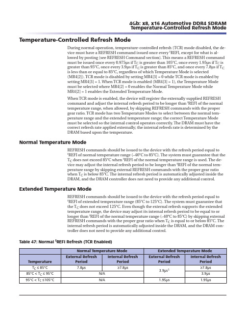
Temperature-Controlled Refresh ModeDuring normal operation, temperature-controlled refresh (TCR) mode disabled, the de-vice must have a REFRESH command issued once every t REFI, except for what is al-lowed by posting (see REFRESH Command section). This means a REFRESH commandmust be issued once every 0.975μs if T C is greater than 105°C, once every 1.95μs if T C isgreater than 95°C, once every 3.9μs if T C is greater than 85°C, and once every 7.8μs if T Cis less than or equal to 85°C, regardless of which Temperature Mode is selected(MR4[2]). TCR mode is disabled by setting MR4[3] = 0 while TCR mode is enabled bysetting MR4[3] = 1. When TCR mode is enabled (MR4[3] = 1), the Temperature Modemust be selected where MR4[2] = 0 enables the Normal Temperature Mode whileMR4[2] = 1 enables the Extended Temperature Mode.When TCR mode is enabled, the device will register the externally supplied REFRESHcommand and adjust the internal refresh period to be longer than t REFI of the normaltemperature range, when allowed, by skipping REFRESH commands with the propergear ratio. TCR mode has two Temperature Modes to select between the normal tem-perature range and the extended temperature range; the correct Temperature Modemust be selected so the internal control operates correctly. The DRAM must have thecorrect refresh rate applied externally; the internal refresh rate is determined by theDRAM based upon the temperature.Normal Temperature ModeREFRESH commands should be issued to the device with the refresh period equal tot REFI of normal temperature range (–40°C to 85°C). The system must guarantee that theT C does not exceed 85°C when t REFI of the normal temperature range is used. The de-vice may adjust the internal refresh period to be longer than t REFI of the normal tem-perature range by skipping external REFRESH commands with the proper gear ratiowhen T C is below 85°C. The internal refresh period is automatically adjusted inside theDRAM, and the DRAM controller does not need to provide any additional control. Extended Temperature ModeREFRESH commands should be issued to the device with the refresh period equal tot REFI of extended temperature range (85°C to 125°C). The system must guarantee thatthe T C does not exceed 125°C. Even though the external refresh supports the extendedtemperature range, the device may adjust its internal refresh period to be equal to orlonger than t REFI of the normal temperature range (–40°C to 85°C) by skipping externalREFRESH commands with the proper gear ratio when T C is equal to or below 85°C. Theinternal refresh period is automatically adjusted inside the DRAM, and the DRAM con-troller does not need to provide any additional control.Table 47: Normal t REFI Refresh (TCR Enabled)Fine Granularity Refresh ModeMode Register and Command Truth TableThe REFRESH cycle time (t RFC) and the average refresh interval (t REFI) can be pro-grammed by the MRS command. The appropriate setting in the mode register will set asingle set of REFRESH cycle times and average refresh interval for the device (fixedmode), or allow the dynamic selection of one of two sets of REFRESH cycle times andaverage refresh interval for the device (on-the-fly mode [OTF]). OTF mode must be ena-bled by MRS before any OTF REFRESH command can be issued.Table 48: MRS DefinitionThere are two types of OTF modes (1x/2x and 1x/4x modes) that are selectable by pro-gramming the appropriate values into the mode register. When either of the two OTFmodes is selected, the device evaluates the BG0 bit when a REFRESH command is is-sued, and depending on the status of BG0, it dynamically switches its internal refreshconfiguration between 1x and 2x (or 1x and 4x) modes, and then executes the corre-sponding REFRESH operation.Table 49: REFRESH Command Truth Tablet REFI and t RFC ParametersThe default refresh rate mode is fixed 1x mode where REFRESH commands should beissued with the normal rate; that is, t REFI1 = t REFI(base) (for T C≤ 85°C), and the dura-tion of each REFRESH command is the normal REFRESH cycle time (t RFC1). In 2xmode (either fixed 2x or OTF 2x mode), REFRESH commands should be issued to thedevice at the double frequency (t REFI2 = t REFI(base)/2) of the normal refresh rate. In 4xmode, the REFRESH command rate should be quadrupled (t REFI4 = t REFI(base)/4). PerFigure 84: TCR Mode Example1Controller85°C T C 95°C T C 85°C REFRESHExternal t REFI3.9μs Internal t REFI 3.9μs Internal t REFI 7.8μs REFRESH REFRESH REFRESH REFRESH REFRESH REFRESHREFRESH REFRESHREFRESH REFRESH REFRESH REFRESH REFRESH REFRESH REFRESH REFRESH REFRESH Note: 1.TCR enabled with Extended Temperature Mode selected.。
- 1、下载文档前请自行甄别文档内容的完整性,平台不提供额外的编辑、内容补充、找答案等附加服务。
- 2、"仅部分预览"的文档,不可在线预览部分如存在完整性等问题,可反馈申请退款(可完整预览的文档不适用该条件!)。
- 3、如文档侵犯您的权益,请联系客服反馈,我们会尽快为您处理(人工客服工作时间:9:00-18:30)。
To all our customers
Regarding the change of names mentioned in the document, such as Mitsubishi Electric and Mitsubishi XX, to Renesas Technology Corp.
The semiconductor operations of Hitachi and Mitsubishi Electric were transferred to Renesas Technology Corporation on April 1st 2003. These operations include microcomputer, logic, analog and discrete devices, and memory chips other than DRAMs (flash memory, SRAMs etc.) Accordingly, although Mitsubishi Electric, Mitsubishi Electric Corporation, Mitsubishi Semiconductors, and other Mitsubishi brand names are mentioned in the document, these names have in fact all been changed to Renesas Technology Corp. Thank you for your understanding. Except for our corporate trademark, logo and corporate statement, no changes whatsoever have been made to the contents of the document, and these changes do not constitute any alteration to the contents of the document itself.
Note : Mitsubishi Electric will continue the business operations of high frequency & optical devices and power devices.
Renesas Technology Corp.
Customer Support Dept.
April 1, 2003
MITSUBISHI MICROCOMPUTERS
3812 Group
SINGLE-CHIP 8-BIT CMOS MICROCOMPUTER
© 2002 MITSUBISHI ELECTRIC CORP.
New publication, effective July 2002.
Specifications subject to change without notice.
REVISION HISTORY3812 GROUP USER’S MANUAL
Rev.Date Description
Page Summary
1.007/10/02The first edition is issued.
(1/X)。