AA3021SESK, 规格书,Datasheet 资料
SAN3021资料

SAN3021PDS038-SA2531/2-004 Rev. B 21-03-00This Application Note describes how to modify the standard application AN1500A to use a dynamic microphone instead of the standard electret microphone. Additionally, an application is shown, which uses the dynamic microphone as tone ringer.• Updating existing systems using dynamic handset microphone• No need for a piezo ringer when using the dynamic microphone as tone ringerTable of Contents1SCOPE.................................................................................................................................................................12KEY FEATURES .................................................................................................................................................13OTHER APPLICABLE DOCUMENTS AND PAPERS........................................................................................14REVISION STATUS.............................................................................................................................................15GENERAL DESCRIPTION. (26)HARDWARE CONFIGURATION (2)6.1U SING THE DYNAMIC MICROPHONE AS TONE RINGER (SCHEMATIC :A ).................................................................2 6.1.1Ringer part.............................................................................................................................................2 6.1.2Microphone amplifier part......................................................................................................................36.2A MPLIFIER FOR GENERAL PURPOSE APPLICATIONS (SCHEMATIC :B )...................................................................37 APPLICATION SCHEMATIC:.. (48)LIABILITY AND COPYRIGHT STATEMENT (5)Application Note AN1500A: SA2532K Single Chip Telephone Demo BoardSAN3021 Application Note (this document)SAN3021 SchematicRev. 1.1SA2531/2 Single Chip Telephone:Using dynamic microphoneas tone ringer1 Scope2 Key Features3 Other applicable documents and papers4 Revision status5 General descriptionDynamic handset microphones have been widely replaced by electret microphones, mainly because of higher output level, low EMC sensitivity and price issues. Therefore, the standard Single Chip Telephone application, AN1500 is based on using an electret handset microphone.However, there are situations where usage of a dynamic microphone is still desired, e.g.•when updating an existing design , using a dynamic handset microphone•when taking advantage of the higher speech quality of dynamic microphones•when using the dynamic microphone as tone ringer6 Hardware configurationGenerally, because of the lower output level of a dynamic microphone (≈10dB less than an electret microphone) the microphone signal must be amplified by a simple 10dB amplifier before it can be fed into the microphone inputs, M1 and M2 of the SA2531/2.In the following schematic, two basic considerations when using dynamic microphones are shown:1. A single ended circuit, which uses the dynamic microphone for both microphone and tone ringer.2. A differential circuit, which is fully balanced, to replace an electret microphone.6.1 Using the Dynamic Microphone as Tone Ringer (Schematic :A)6.1.1 Ringer partThe piezo tone ringer used in AN1500 can be replaced by a dynamic microphone, when close attention is paid to the following considerations :Since a maximum sound pressure is required in ringing mode, the maximum DC current and AC levelfor the type of dynamic microphone used must not be exceeded.To limit the output of the ringer amplifier Q4, the zener diode D4 should be reduced to 15V . R18 limits the output current, it can also be used to set the ringer volume.Since the microphone (= the ringer) is connected single ended to V DD, any noise on V DD would be amplified by the microphone amplifier, causing higher noise for the transmitted signal. Therefore, D6 and C10 are added to reference the microphone amplifier input to V SS (over C10) but at the same time keep the DC level above V DD in ringing mode.The ringer cannot be referenced to V SS, because it would discharge V DD during ringing!With the application shown, the anode of D6 will be V DD+0.7V, because during ringing V DD is supplied over the ringing capacitor. (not shown).6.1.2 Microphone AmplifierQ5 is a simple “classic” amplifier, which amplifies the single ended signal by ≈10dB. Gain can be adjusted by varying R21. R23 is the feedback resistor to set a stable DC bias point. R24 and R25 are setting the base voltage. The transistor type used (in this case BC549) should be a general purpose low noise transistor.The single ended signal is decoupled by C17. R26 is required to limit the input current to the amplifier during ringing.C15 and C16 are EMC capacitors to limit the bandwidth of the amplifier. Frequencies >10kHz are being attenuated.The amplifier is supplied by (the initial electret microphone supply) R20 and C14. C14 should be increased to 220µF. Since this supply is derived from the line output, there will be some small ripple from the transmitted signal at C14.In order not to form a positive feedback loop from LI over the microphone supply, Q5 and the internal microphone amplifier (M1/M2 to LI) , care must be taken to connect M1/M2 inputs in the correct manner as shown in the application.With this connection, a negative feedback loop is formed, rejecting any ripple on C14.Because of the unbalanced, single ended structure of this amplifier, its input is very sensitive. Therefore it is recommended to use this application only in one-piece telephones with shortest possible wires between microphone and amplifier !6.2 Amplifier for General Purpose Applications (Schematic :B)This amplifier is similar to the amplifier described in pt. 6.1, however the microphone is balanced (RR23B and RR26 = 2kΩ).Amplifier gain = RR21 / RR23B = 3:1 = 10dB.This application can directly replace an electret microphone. Because of the differential, balanced structure of the amplifier input , it is also suitable for longer distances between microphone and amplifier, e.g. corded handsets.SAN30214/57 Application schematic:元器件交易网元器件交易网SAN30218 Liability and Copyright StatementDisclaimer:The information contained in this document is confidential and proprietary to South African Micro-Electronic Systems (Pty) Ltd ("SAMES”) and may not be copied or disclosed to a third party, in whole or in part, without the express written consent of SAMES. The information contained herein is current as of the date of publication; however, delivery of this document shall not under any circumstances create any implication that the information contained herein is correct as of any time subsequent to such date. SAMES does not undertake to inform any recipient of this document of any changes in the information contained herein, and SAMES expressly reserves the right to make changes in such information, without notification,even if such changes would render information contained herein inaccurate or incomplete. SAMES makes no representation or warranty that any circuit designed by reference to the information contained herein, will function without errors and as intended by the designer.South African Micro-Electronic Systems (Pty) LtdP O Box 15888,33 Eland Street,Lynn East,Koedoespoort Industrial Area,0039Pretoria,Republic of South Africa,Republic of South AfricaTel: 012 333-6021Tel:Int +27 12 333-6021Fax: 012 333-3158Fax:Int +27 12 333-3158Web Site : http://www.sames.co.za。
Agilent U2300A Series USB模块多功能数据采集设备数据表说明书

AgilentU2300A Series USB Modular Multifunction Data Acquisition DevicesData SheetFeatures• Up to 3 MSa/s sampling rate for a single channel • Functions as astandalone or modular unit• Easy to use—plug-and- play and hot-swappable with Hi-Speed USB 2.0• Up to 384 channels when incorporated into U2781A Agilent modular instrument chassis• Easy-to-use bundledsoftware for quick setupand data logging to PC • 12-bit or 16-bit A/Dresolution• 24-bit programmabledigital input/output• Self-calibrationcapability• Compatible with a widerange of ApplicationDevelopmentEnvironments• USBTMC 488.2 standards IntroductionAgilent U2300A Series USB modularmultifunction data acquisition (DAQ)devices are a high performance PCdata acquisition solution. The U2300ASeries DAQ devices consist of twofamilies—basic multifunction DAQand high density multifunction DAQ.The basic multifunction DAQ familycomes in four models while the highdensity multifunction DAQ family ismade up of three models.The U2300A Series DAQ devicesapplications extend across industrialand education environments. TheDAQ device is well suited for researchand development, manufacturing anddesign validation engineers, whorequire measurement devices with fastsampling rate.High Sampling RateThe U2300A Series DAQ devices havesampling rate of up to 3 MSa/s for asingle channel. When multiplechannels are confi gured, it cansample data up to 1 MSa/s. This fastsampling capability allows users toperform intermittent detection easily.This also makes it ideal when dealingwith high density analog input/outputsignals, especially with different inputranges and sampling requirements.Flexible Standalone orModular CapabilityThe U2300A Series DAQ devices areuniquely designed for the fl exibilityof functioning as a standalone ormodular unit. When used with theU2781A modular instrument chassis,the number of channels can reach upto 384 channels.Ease of UseThe U2300A Series DAQ devices areequipped with Hi-Speed USB 2.0interface for easy setup, plug-and-play,and hot swappable connectivity. Itsease-of-use makes it ideal for theeducation environment. Simplifyingthis further is the AgilentMeasurement Manager software thatoffers a simple interface for quicksetup, confi guration and measurementcontrol.Flexible System andControl OptionsPolling and continuous modeThe U2300A Series DAQ devices pro-vide two modes, the polling mode andthe continuous mode. The continuousmode has the ability to acquire datacontinuously once the trigger signal isreceived.Trigger sourcesU2300 Series offers immediate trigger (none), analog/external digital trigger, System Synchronous Interface (SSI)/star trigger and master/slave trigger sources. All these triggeroptions give you the capability to confi gure trigger sources during A/D and D/A operations. Master/slave trigger and SSI/star trigger are rec-ommended when USB modules are slotted into the Agilent U2781A USB modular instrument chassis.Predefi ned function generatorThe two analog output channelsoffered does not only provide DC voltage but also are capable of generating common and predefi ned waveforms such as sinusoid wave, square wave, triangle wave, sawtooth wave and noise wave.Arbitrary WaveformU2300A Series supports arbitrary waveform, which allows user to generate arbitrary waveform via Agilent Measurement Manager application software or SCPI command.Burst modeBurst mode is an enhancement feature of U2300 Series DAQ that enable the DAQ to simulate in simultaneous mode for analog input acquisition. This enable users to perform sampling measurement up to the highest speedof the DAQ capability.Figure 1. Agilent Measurement Manager application software user interface Compatible with wide range of Application Development EnvironmentsThe Agilent U2300A DAQ devices are compatible with a wide range ofApplication Development Environments. This minimizes all the time taken by R&D and manufacturing engineers to use the devices in different software environments as they can program directly using SCPI commands.Listed below are the popular development environments and tools that the DAQ device is compatible with:• Agilent VEE and Agilent T&M Toolkit• Microsoft Visual , C/C++ and Visual Basic 6• LabVIEW• MATLAB® (Agilent U2300A Adaptor is available at /fi nd/U2300A) For more information, please visit /fi nd/U2300A.Product Characteristics and General Specifi cations REMOTE INTERFACE• Hi-Speed USB 2.0• USBTMC class devicePOWER REQUIREMENT• +12 VDC (TYPICAL)• 2 A (MAX) input rated currentPOWER CONSUMPTION+12 VDC, 550 mA maximumOPERATING ENVIRONMENT• Operating temperature from 0 °C to +55 °C• Relative humidity at 15% to 85% RH (non-condensing)• Altitude up to 2000 meters• Pollution Degree 2• For indoor use onlySTORAGE COMPLIANCE–20 °C to 70 °CSAFETY COMPLIANCECertifi ed with:• IEC 61010-1:2001/EN 61010-1:2001 (2nd Edition)• USA: UL61010-1: 2004• Canada: CSA C22.2 No.61010-1:2004EMC COMPLIANCE• IEC/EN 61326-1 1998• CISPR 11: 1990/EN55011:1991, Class A, Group 1• CANADA: ICES-001: 1998• Australia/New Zealand: AS/NZS 2064.1SHOCK AND VIBRATIONTested to IEC/EN 60068-2IO CONNECTOR68-pin female VHDCI TypeDIMENSION (WxDxH)• 120.00 mm x 182.40 mm x 44.00 mm (with plastic casing)• 105.00 mm x 174.54 mm x 25.00 mm (without plastic casing)WEIGHT• 565 g (with plastic casing)• 400 g (without plastic casing)WARRANTYThree yearsSystem RequirementsPROCESSOR1.6 GHz Pentium IV or higherOPERATING SYSTEMOne of the following Microsoft® Windows® versions:• Windows XP Professional or Home Edition (Service Pack 1 or later)• Windows 2000 Professional (Service Pack 4 or later)BROWSERMicrosoft Internet Explorer 5.01 or higherAVAILABLE RAM512 MB or higher recommendedHARD DISK SPACE1 GBPREREQUISITES• Agilent IO Libraries Suite 14.2[1] or higher• Agilent T&M Toolkit 2.1 Runtime version[2]• Microsoft .NET Framework version 1.0 and 2.0[2][1] Available in Agilent Automation-Ready CD[2] Bundled with Agilent Measurement Manager software application installer Product Outlook and Dimension Front ViewRear ViewStandard Shipped Items• AC/DC Power Adapter• Power Cord• USB Extension Cable• L-Mount Kit (used with modularinstrument chassis)• Agilent U2300A Series DataAcquisition Devices and AgilentMeasurement Manager Quick Start Guide• Agilent USB Modular InstrumentU2300A & U2700A Series ProductReference CD-ROM• Agilent Automation-Ready CD (containsthe Agilent IO Libraries Suite)• Certifi cate of CalibrationOptional Accessories• U2901A Terminal block and SCSI-II 68-pinconnector with 1-meter cable• U2902A Terminal block and SCSI-II 68-pinconnector with 2-meter cable• U2718A 6-slot USB modular instrumentchassisElectrical Specifi cations[1] System Scynchronous Interface (SSI) and star trigger commands are used when the modular device is incorporated into the chassis.[2] Maximum external reference voltage for analog output channels (AO_EXT_REF) is ±10 V.[3] 20 minutes warm-up time is recommended.[1] System Synchronous Interface (SSI) and star trigger commands are used when the modular device is incorporated into the chassis.[2] Maximum external reference voltage for analog output channels (AO_EXT_REF) is ±10 V.[3] 20 minutes warm-up time is recommended.Electrical Measurement Specifi cations[1] Specifi cations are for 20 minutes of warm-up time, calibration temperature at 23 °C and input range of ±10 V.[2] Specifi cations are based on the following test conditions.Dynamic Range Test Model Number Test Conditions (DUT setting at ±10 V bipolar)• –3 dB small signal bandwidth • 1% THD large signal bandwidth U2351AU2352ASampling Rate:Input voltage:• –3 dB small signal bandwidth• 1% THD large signal bandwidth250 kSa/s10% FSRFSR –1 dB FS U2353AU2354ASampling Rate:Input voltage:• –3 dB small signal bandwidth• 1% THD large signal bandwidth500 kSa/s10% FSRFSR –1 dB FS[3] Specifi cations are based on the following test conditions.Dynamic Range Test Model Number Test Conditions (DUT setting at ±10 V bipolar)SFDR, THD, SINAD, SNR, ENOB U2351AU2352ASampling Rate:Fundamental Frequency:Number of points:Fundamental input voltage:250 kSa/s2.4109 kHz8192FSR –1 dB FS U2353AU2354ASampling Rate:Fundamental Frequency:Number of points:Fundamental input voltage:500 kSa/s4.974 kHz16384FSR –1 dB FS[1] Specifi cations are for 20 minutes of warm-up time, calibration temperature at 23 °C and input range of ±10 V.[2] Specifi cations are based on the following test conditions.Dynamic Range Test Model Number Test Conditions (DUT setting at ±10 V bipolar)• –3 dB small signal bandwidth • 1% THD large signal bandwidth U2355A Sampling Rate:Input voltage:• –3 dB small signal bandwidth• 1% THD large signal bandwidth250 kSa/s10% FSRFSR –1 dB FS U2356A Sampling Rate:Input voltage:• –3 dB small signal bandwidth• 1% THD large signal bandwidth500 kSa/s10% FSRFSR –1 dB FS U2331A Sampling Rate:Input voltage:• –3 dB small signal bandwidth• 1% THD large signal bandwidth3 MSa/s10% FSRFSR –1 dB FS[3] Specifi cations are based on the following test conditions.Dynamic Range Test Model Number Test Conditions (DUT setting at ±10 V bipolar)• –3 dB small signal bandwidth • 1% THD large signal bandwidth U2355A Sampling Rate:Fundamental Frequency:Number of points:Fundamental input voltage:250 kSa/s2.4109 kHz8192FSR –1 dB FS U2356A Sampling Rate:Fundamental Frequency:Number of points:Fundamental input voltage:500 kSa/s4.974 kHz16384FSR –1 dB FS U2331A Sampling Rate:Fundamental Frequency:Number of points:Fundamental input voltage:3 MSa/s29.892 kHz65536FSR –1 dB FSDC CharacteristicsAccuracy Specifi cationsAnalog Input1. The above specifi cations are typical for 23°C.2. Specifi cations are for 20 minutes warm-up and self calibration.3. The measurements are calculated with 100 points averaging of data.[1] Offset error is measured at midscale of full scale range.[2] Accuracy = +/– [% of |(Gain Error / (Measured value – Midscale of FSR))| + Offset Error]1. The above specifi cations are typical for 23°C.2. Specifi cations are for 20 minutes warm-up and self calibration.3. The measurements are calculated with 100 points averaging of data.[1] Offset error is measured at midscale of full scale range.[2] Accuracy = +/– [% of |(Gain Error / (Measured value – Midscale of FSR))| + Offset Error] Analog Output1. The above specifi cations are typical for 23°C.2. Specifi cations are for 20 minutes warm-up and self calibration.[1] Offset error is measured at 0 V.[2] Accuracy = +/– [% of |Gain Error/Output value| + offset voltage]Product specifi cations and descriptions in this document subject to change without notice.© Agilent Technologies, Inc. 2006, 2007Printed in USA, April 30, 20075989-5626EN。
SI2302-TP;中文规格书,Datasheet资料

Revision: A
/
3 of 5
2011/01/01
VGS, Gate to Source Voltage (V) ID, Drain Current (A)
VTH, Normalized Gate-Source Threshold Voltage
RDS(ON), Normalized RDS(ON), On-Resistance(Ohms)
IS, Source-drain current (A)
ID, Drain Current (A)
SI2302
10 25 C
Maximum Ratings @ 25OC Unless Otherwise Specified
Symbol VDS ID IDM VGS
PD R©JA
TJ
TSTG
Parameter Drain-source Voltage Drain Current-Continuous Drain Current-Pulsed a Gate-source Voltage
MCC
TM
Micro Commercial Components
5 VDS=10V ID=3.6A
4
3
2
1
0
0
2
4
6
Qg, Total Gate Charge (nC)
Figure 7. Gate Charge
VDD
RL VIN
D
VOUT
VGS
RGEN G
S
Figure 9. Switching Test Circuit
74271112S;中文规格书,Datasheet资料
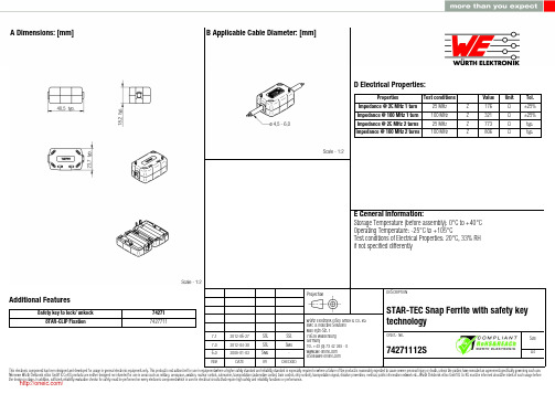
7.1 7.0 6.02012-06-272012-04-302008-01-03SStSStSMuSStSMu-Würth Elektronik eiSos GmbH & Co. KGEMC & Inductive SolutionsMax-Eyth-Str. 174638 WaldenburgGermanyTel. +49 (0) 79 42 945 - 0A Dimensions: [mm] Additional FeaturesSafety key to lock/ unkock STAR-CLIP Fixation74271 7427711D2 General Properties:Ferrite core Ferrite core Ferrite core Plastic housing Plastic housing Test cable Test cablePropertiesMaterial Initial permeability Curie temperatureColourFlammability ClassificationApplicable cable Applicable cable lengthµi T CValue 4 W 620620150Black UL94-V0AWG2690Unit°Cmm Tol.typ.typ.F Typical Impedance Characteristics:I Cautions and Warnings:The following conditions apply to all goods within the product series of WE-STAR TECof Würth Elektronik eiSos GmbH & Co. KG:General:All recommendations according to the general technical specifications of the data sheet have to be complied with.The disposal and operation of the product within ambient conditions which probably alloy or harm the component surface has to be avoided.The packaging of the product is to encase the needed humidity of the plastic housing. To ensure the humidity level, the products have to be stored in this delivered packaging. If not, the products are losing their humidity. In this case you can re-condition the components according to the internal standard WE1883 to ensure the necessary humidity in the plastic.To ensure the operating mode of the product, the ambient temperature at processing (when the part will be mounted on the cable) has to be in the range of 15 to 25 °C.Before mounting, the part should be stored for one hour in this condition.The responsibility for the applicability of customer specific products and the use in a particular customer design is always within the authority of the customer. All technical specifications for standard products do also apply for customer specific products.Direct mechanical impact to the product and the forcible closing of this shall be prevented as the ferrite material of the ferrite body or the pla-stic housing could flake or in the worst case it could break.Product specific:Follow all instructions mentioned in the datasheet, especially:•The cable diameter must be pointed out, otherwise no warranty will be sustained.•Violation of the technical product specifications such as exceeding the nominal rated current will result in the loss of warranty.1. General Customer ResponsibilitySome goods within the product range of Würth Elektronik eiSos GmbH & Co. KG contain statements regarding general suitability for certain application areas. These statements about suitability are based on our knowledge and experience of typical requirements concerning the are-as, serve as general guidance and cannot be estimated as binding statements about the suitability for a customer application. The responsibi-lity for the applicability and use in a particular customer design is always solely within the authority of the customer. Due to this fact it is up to the customer to evaluate, where appropriate to investigate and decide whether the device with the specific product characteristics described in the product specification is valid and suitable for the respective customer application or not.2. Customer Responsibility related to Specific, in particular Safety-Relevant ApplicationsIt has to be clearly pointed out that the possibility of a malfunction of electronic components or failure before the end of the usual lifetime can-not be completely eliminated in the current state of the art, even if the products are operated within the range of the specifications.In certain customer applications requiring a very high level of safety and especially in customer applications in which the malfunction or failure of an electronic component could endanger human life or health it must be ensured by most advanced technological aid of suitable design of the customer application that no injury or damage is caused to third parties in the event of malfunction or failure of an electronic component.3. Best Care and AttentionAny product-specific notes, warnings and cautions must be strictly observed.4. Customer Support for Product SpecificationsSome products within the product range may contain substances which are subject to restrictions in certain jurisdictions in order to serve spe-cific technical requirements. Necessary information is available on request. In this case the field sales engineer or the internal sales person in charge should be contacted who will be happy to support in this matter.5. Product R&DDue to constant product improvement product specifications may change from time to time. As a standard reporting procedure of the Product Change Notification (PCN) according to the JEDEC-Standard inform about minor and major changes. In case of further queries regarding the PCN, the field sales engineer or the internal sales person in charge should be contacted. The basic responsibility of the customer as per Secti-on 1 and 2 remains unaffected.6. Product Life CycleDue to technical progress and economical evaluation we also reserve the right to discontinue production and delivery of products. As a stan-dard reporting procedure of the Product Termination Notification (PTN) according to the JEDEC-Standard we will inform at an early stage about inevitable product discontinuance. According to this we cannot guarantee that all products within our product range will always be available. Therefore it needs to be verified with the field sales engineer or the internal sales person in charge about the current product availability ex-pectancy before or when the product for application design-in disposal is considered.The approach named above does not apply in the case of individual agreements deviating from the foregoing for customer-specific products.7. Property RightsAll the rights for contractual products produced by Würth Elektronik eiSos GmbH & Co. KG on the basis of ideas, development contracts as well as models or templates that are subject to copyright, patent or commercial protection supplied to the customer will remain with Würth Elektronik eiSos GmbH & Co. KG.8. General Terms and ConditionsUnless otherwise agreed in individual contracts, all orders are subject to the current version of the “General Terms and Conditions of Würth Elektronik eiSos Group”, last version available at .J Important Notes:The following conditions apply to all goods within the product range of Würth Elektronik eiSos GmbH & Co. KG:分销商库存信息: WURTH-ELECTRONICS 74271112S。
AMIS30621AUA;中文规格书,Datasheet资料

AMIS-30621Micro-Stepping Motor Driver INTRODUCTIONThe AMIS−30621 is a single−chip micro−stepping motor driver with position controller and control/diagnostic interface. It is ready to build dedicated mechatronics solutions connected remotely with a LIN master.The chip receives positioning instructions through the bus and subsequently drives the motor coils to the desired position. The on−chip position controller is configurable (OTP or RAM) for different motor types, positioning ranges and parameters for speed, acceleration and deceleration. The AMIS−30621 acts as a slave on the LIN bus and the master can fetch specific status information like actual position, error flags, etc. from each individual slave node. The chip is implemented in I2T100 technology, enabling both high voltage analog circuitry and digital functionality on the same chip. The AMIS−30621 is fully compatible with the automotive voltage requirements.PRODUCT FEATURESMotordriver•Micro−Stepping Technology•Peak Current Up to 800 mA•Fixed Frequency PWM Current−Control•Automatic Selection of Fast and Slow Decay Mode•No External Fly−Back Diodes Required•Compliant with 14 V Automotive Systems and Industrial Systems Up to 24 VController with RAM and OTP Memory•Position Controller•Configurable Speeds and Acceleration•Input to Connect Optional Motion SwitchLIN Interface•Physical Layer Compliant to LIN rev. 2.0. Data−Link Layer Compatible with LIN Rev. 1.3 (Note 1)•Field−Programmable Node Addresses •Dynamically Allocated Identifiers •Diagnostics and Status InformationProtection•Overcurrent Protection•Undervoltage Management•Open−Circuit Detection•High Temperature Warning and Management •Low Temperature Flag•LIN Bus Short−Circuit Protection to Supply and Ground •Lost LIN Safe Operation Power Saving•Powerdown Supply Current < 50 m A•5 V Regulator with Wake−up on LIN ActivityEMI Compatibility•LIN Bus Integrated Slope Control•HV Outputs with Slope Control •These are Pb−Free Devices1.Minor exceptions to the conformance of the data−link layer to LIN rev. 1.3.See detailed ordering and shipping information in the package dimensions section on page 2 of this data sheet.ORDERING INFORMATIONSOIC−203 & 7 SUFFIXCASE 751AQNQFP−326 SUFFIXCASE 560AA*For additional information on our Pb−Free strategy and soldering details, please download the ON Semiconductor Soldering and Mounting T echniques Reference Manual, SOLDERRM/D.APPLICATIONSThe AMIS−30621 is ideally suited for small positioning applications. Target markets include: automotive (headlamp alignment, HV AC, idle control, cruise control), industrial equipment (lighting, fluid control, labeling, process control, XYZ tables, robots...) and building automation (HV AC,surveillance, satellite dish, renewable energy systems). Suitable applications typically have multiple axes or require mechatronic solutions with the driver chip mounted directly on the motor.Table 1. ORDERING INFORMATIONPart No.Peak Current UV*Package Shipping†AMIS30621C6213G800 mA High SOIC−20(Pb−Free)Tube / TrayAMIS30621C6213RG800 mA High Tape & ReelAMIS30621C6216G800 mA Low NQFP−32 (7 x 7 mm)(Pb−Free)Tube / TrayAMIS30621C6216RG800 mA Low Tape & ReelAMIS30621C6217G**800 mA Low SOIC−20(Pb−Free)Tube / TrayAMIS30621C6217RG**800 mA Low Tape & Reel†For information on tape and reel specifications, including part orientation and tape sizes, please refer to our Tape and Reel Packaging Specification Brochure, BRD8011/D.*UV undervoltage lock out levels: see DC Parameters UV1 & UV2 (Stop Voltage thresholds).** For prodcut versions AMIS30621C6217G and AMIS30621C6217RG the Ihold0 bit in OTP is programmed to ‘1’.QUICK REFERENCE DATATable 2. ABSOLUTE MAXIMUM RATINGSSymbol Parameter Min Max UnitV BB, VHW2, VSWI Supply voltage, Hardwired Address and SWI Pins−0.3+40(Note 1)VV lin Bus input voltage−40+40VT J Junction temperature range (Note 2)−50+175°CT st Storage temperature−55+160°CV esd Human Body Model Electrostatic discharge voltage on LINpin (Note 3)−4+4kVHuman Body Model Electrostatic discharge voltage on otherpins (Note 3)−2+2kV CDM Electrostatic discharge voltage on other pins (Note 4)−500+500VStresses exceeding Maximum Ratings may damage the device. Maximum Ratings are stress ratings only. Functional operation above the Recommended Operating Conditions is not implied. Extended exposure to stresses above the Recommended Operating Conditions may affect device reliability.1.For limited time: V BB < 0.5 s, SWI and HW2 pins < 1.0 s.2.The circuit functionality is not guaranteed.3.Human Body Model according to MIL−STD−883 Method 3015.7, measured on SOIC devices, and according to AEC−Q100:EIA−JESD22−A114−B (100 pF via 1.5 k W) measured on NQFP device.4.CDM according to EOS_ESD−DS5.3−1993 (draft)−socketed mode, measured on SOIC devices, and according to AEC−Q100:EIA−JESD22−A115−A measured on NQFP devices.Table 3. OPERATING RANGESSymbol Parameter Min Max UnitV BB Supply voltage+6.5+29VT J Operating temperature range (Note 5)−40+165°C5.Note that the thermal warning and shutdown will get active at the level specified in the “DC Parameters”.No more than 100 cumulated hoursin life time above T tw.Table of ContentsGeneral Description 1. . . . . . . . . . . . . . . . . . . . . . . . . . . . Product Features 1. . . . . . . . . . . . . . . . . . . . . . . . . . . . . . Applications 2. . . . . . . . . . . . . . . . . . . . . . . . . . . . . . . . . . Ordering Information 2. . . . . . . . . . . . . . . . . . . . . . . . . . . Quick Reference Data 2. . . . . . . . . . . . . . . . . . . . . . . . . . Maximum Ratings 2. . . . . . . . . . . . . . . . . . . . . . . . . . . . . Block Diagram 3. . . . . . . . . . . . . . . . . . . . . . . . . . . . . . . . Pin Description 4. . . . . . . . . . . . . . . . . . . . . . . . . . . . . . . Package Thermal Resistance 5. . . . . . . . . . . . . . . . . . . . .DC Parameters 6. . . . . . . . . . . . . . . . . . . . . . . . . . . . . . . . AC Parameters 8. . . . . . . . . . . . . . . . . . . . . . . . . . . . . . . . Typical Application 9. . . . . . . . . . . . . . . . . . . . . . . . . . . . Positioning Parameters 10. . . . . . . . . . . . . . . . . . . . . . . . Structural Description 13. . . . . . . . . . . . . . . . . . . . . . . . . Functions Description 14. . . . . . . . . . . . . . . . . . . . . . . . . Lin Controller 33. . . . . . . . . . . . . . . . . . . . . . . . . . . . . . . LIN Application Commands 42. . . . . . . . . . . . . . . . . . . . Package Outline 57. . . . . . . . . . . . . . . . . . . . . . . . . . . . . . Figure 1. Block DiagramTSTLINMOTXP MOTXNHW[2:0]MOTYP MOTYNXP VBB SWI NC HW0XP VBB VBB CPNCPP VCP YN VBB YN VBB VBB YPXNGND GNDXNYPGNDGNDHW1VDDGNDTSTLINHW2GNDNCHW0GND SWI GND HW1MOTXP VBB VDD GND GND MOTXN MOTYP MOTYN TST LIN HW2CPN CPPVBB VCPFigure 2. SOIC −20 and NQFP −32 Pin −outNQFP −32Table 4. PIN DESCRIPTIONPin Name Pin DescriptionSOIC −20NQFP −32HW0Bit 0 of LIN −ADD To be Tied to GND or V DD18HW1Bit 1 of LIN −ADD29V DD Internal supply (needs external decoupling capacitor)310GND Ground, heat sink4,7,14,1711, 14, 25, 26, 31, 32TST Test pin (to be tied to ground in normal operation)512LIN LIN −bus connection 613HW2Bit 2 LIN −ADD815CPN Negative connection of pump capacitor (charge pump)917CPP Positive connection of pump −capacitor (charge pump)1018VCP Charge −pump filter −capacitor 1119V BB Battery voltage supply 12,193, 4, 5, 20, 21, 22MOTYN Negative end of phase Y coil 1323, 24MOTYP Positive end of phase Y coil 1527, 28MOTXN Negative end of phase X coil 1629, 30MOTXP Positive end of phase X coil 181, 2SWI Switch input206NCNot connected (to be tied to ground)7, 16PACKAGE THERMAL RESISTANCEThe AMIS −30621 is available in SOIC −20 and optimized NQFP32 packages. For cooling optimizations, the NQFP has an exposed thermal pad which has to be soldered to the PCB ground plane. The ground plane needs thermal vias to conduct the head to the bottom layer. Figures 3 and 4 give examples for good power distribution solutions.For precise thermal cooling calculations the major thermal resistances of the devices are given. The thermal media to which the power of the devices has to be given are:•Static environmental air (via the case)•PCB board copper area (via the device pins and exposed pad)The thermal resistances are presented in Table 5: DC Parameters.The major thermal resistances of the device are the Rth from the junction to the ambient (Rthja) and the overall Rth from the junction to the leads (Rthjp).The NQFP device is designed to provide superior thermal performance. Using an exposed die pad on the bottom surface of the package, is mainly contributing to this performance. In order to take full advantage of the exposed pad, it is most important that the PCB has features to conduct heat away from the package. A thermal grounded pad with thermal vias can achieve this.In below table, one can find the values for the Rthja and Rthjp, simulated according to the JESD −51standard:Package RthJunction −to −Leads and Exposed Pad (Rthjp)RthJunction −to −Leads(Rthjp)RthJunction −to −AmbientRthja 1S0PRthJunction −to −AmbientRthja 2S2PSOIC −20 196239NQFP −320.956030The Rthja for 2S2P is simulated conform to JESD −51 as follows:•A 4−layer printed circuit board with inner power planes and outer (top and bottom) signal layers is used •Board thickness is 1.46 mm (FR4 PCB material)•The 2 signal layers: 70 m m thick copper with an area of 5500 mm2 copper and 20% conductivity•The 2 power internal planes: 36 m m thick copper with an area of 5500 mm 2 copper and 90% conductivityThe Rthja for 1S0P is simulated conform to JESD −51 as follows:•A 1−layer printed circuit board with only 1 layer •Board thickness is 1.46 mm (FR4 PCB material)•The layer has a thickness of 70 m m copper with an area of 5500 mm 2 copper and 20% conductivityFigure 3. Example of SOIC −20 PCB Ground Plane Layout (Preferred Layout at Top and Bottom)Figure 4. Example of NQFP −32 PCB Ground Plane Layout (Preferred Layout at Top and Bottom)DC PARAMETERSThe DC parameters are guaranteed over temperature and V BB in the operating range, unless otherwise specified. Convention: currents flowing into the circuit are defined as positive.Table 5. DC PARAMETERSSymbol Pins Parameter Test Conditions Min Typ Max Unit MOTORDRIVERI MSmax,PeakMOTXPMOTXNMOTYPMOTYN Max current through motorcoil in normal operationV BB = 14 V800mAI MSmax,RMS Max RMS Current ThroughCoil in Normal OperationV BB = 14 V570mAI MSabs Absolute Error on Coil Current(Note 6)V BB = 14 V−1010%I MSrel Matching of X and Y CoilCurrentsV BB = 14 V−707%R DS(on)On Resistance for Each MotorPin at I MSmax (Note 7)V BB = 12 V, T J = 50°C0.501W V BB = 8 V, T J = 50°C0.551W V BB = 12 V, T J = 150°C0.701W V BB = 8 V, T J = 150°C0.851WI MSL Pull down current HiZ Mode, V BB = 7.7 V0.4 2.2mA LIN TRANSMITTERI bus_offLIN Dominant State, Driver Off V bus = 0 V, V BB = 8 V and 18 V−1mAI bus_off Recessive State, Driver Off V bus = V bat,V BB = 8 V and 18 V20m A I bus_lim Current Limitation V BB = 8 V and 18 V5075130mA R slave Pullup Resistance V BB = 8 V and 18 V203047k W LIN RECEIVERV bus_domLIN Receiver Dominant State V BB = 8 V and 18 V00.4 * V BB VV bus_rec Receiver Recessive State V BB = 8 V and 18 V0.6 * V BB V BB V V bus_hys Receiver Hysteresis V BB = 8 V and 18 V0.05 * V BB0.175 * V BB V THERMAL WARNING AND SHUTDOWNT tw Thermal warning138145152°C T tsd Thermal shutdown(Notes 8 and 9)T tw + 10°CT low Low temperature warning(Note 9)T tw− 152°C SUPPLY AND VOLTAGE REGULATORV BBOTPV BB Supply voltage for OTPzapping (Note 10)9.010.0VUV1Stop voltage high threshold Product versions with low UV;See Ordering Information7.78.38.9V UV2Stop voltage low threshold7.07.58.0V UV1Stop voltage high threshold Product versions with high UV;See Ordering Information8.89.39.8V UV2Stop voltage low threshold8.18.58.9V I bat Total current consumption Unloaded outputsV BB = 29 V1 3.5010.0mAI bat_s Sleep mode currentconsumptionV BB = 8 V and 18 V40100m AV DDV DD Regulated internal supply(Note 11)8 V < V BB < 29 V 4.755 5.25VV DDReset Digital supply reset level @powerdown (Note 12)4.5VI DDLim Current limitation Pin shorted to groundV BB = 14 V40mATable 5. DC PARAMETERSSymbol UnitMaxTypMinTest ConditionsParameterPinsSWITCH INPUT AND HARDWIRE ADDRESS INPUTRt_OFFSWI HW2Switch OPEN Resistance(Note 13)10k WRt_ON Switch ON Resistance(Note 13)Switch to GND or V BB2k WV BB_sw V BB range for guaranteedoperation of SWI and HW2629VI lim_sw Current limitation Short to GND or V batV BB = 29 V45mA HARDWIRED ADDRESS INPUTS AND TEST PINV highHW0HW1 TST Input level high V BB = 14 V0.7 * V DD VV low Input level low V BB = 14 V0.3 * V DD V HW hyst Hysteresis V BB = 14 V0.075 * V DD V CHARGE PUMPV CPVCP Output voltage7 V < V BB v 14 V 2 * V BB−2.5V14 V < V BB V BB + 10V BB + 15VC buffer External buffer capacitor220470nF C pump CPP CPN External pump capacitor220470nF PACKAGE THERMAL RESISTANCE VALUESRth ja SO Thermal resistancejunction−to−ambient (2S2P)Simulated conform JEDECJES.D5139K/WRth jp SO Thermal resistancejunction−to−leads19K/WRth ja NQ Thermal resistancejunction−to−ambient (2S2P)30K/WRth jpNQ Thermal resistancejunction−to−leads andexposed pad0.95K/W6.Tested in production for 800 mA, 400 mA, 200 mA and 100 mA current settings for both X and Y coil.7.Based on characterization data.8.No more than 100 cumulated hours in life time above T tw.9.Thermal shutdown and low temperature warning are derived from thermal warning. Guaranteed by design.10.A buffer capacitor of minimum 100 m F is needed between V BB and GND. Short connections to the power supply are recommended.11.Pin V DD must not be used for any external supply12.The RAM content will not be altered above this voltage.13.External resistance value seen from pin SWI or HW2, including 1 k W series resistor. For the switch OPEN, the maximum allowed leakagecurrent is represented by a minimum resistance seen from the pin.AC PARAMETERSThe AC parameters are guaranteed for temperature and V BB in the operating range unless otherwise specified.The LIN transmitter and receiver physical layer parameters are compliant to LIN rev. 2.0 & 2.1.Table 6. AC PARAMETERSSymbol Pins Parameter Test Conditions Min Typ Max Unit POWERUPT pu Powerup Time Guaranteed by Design10ms INTERNAL OSCILLATORf osc Frequency of Internal Oscillator V BB = 14 V 3.6 4.0 4.4MHz LIN TRANSMITTER CHARACTERISTICS ACCORDING TO LIN V2.0 & V2.1D1LIN Duty Cycle 1 = t Bus_rec(min)/(2 x t Bit); See Figure 5THRec(max)= 0.744 x V BBTHDom(max)= 0.581 x V BB;V BB = 7.0 V...18 V; t Bit =50 m s0.396D2Duty Cycle 2 = t Bus_rec(max)/(2 x t Bit); See Figure 5THRec(min)= 0.284 x V BBTHDom(min)= 0.422 x V BB;V BB = 7.6 V...18 V;t Bit = 50 m s0.581LIN RECEIVER CHARACTERISTICS ACCORDING TO LIN V2.0 & V2.1trx_pdrLIN Propagation delay bus dominantto RxD = LowV BB = 7.0 V & 18 V;See Figure 56m strx_pdf Propagation delay bus recess-ive to RxD = High V BB = 7.0 V & 18 V;See Figure 56m strx_sym Symmetry of receiver propaga-tion delaytrx_pdr – trx_pdf−2+2m s SWITCH INPUT AND HARDWIRE ADDRESS INPUTT sw SWIHW2Scan pulse period (Note 14)V BB = 14 V1024m sT sw_on Scan pulse duration (Note 14)V BB = 14 V64m s MOTORDRIVERF pwmMOTxx PWM frequency (Note 14)182022.0kHzT brise Turn−on transient time Between 10% and 90%V BB = 14 V 150nsT bfall Turn−off transient time140ns T stab Run current stabilization time(Note 14)1/Vmin s CHARGE PUMPf CP CPNCPP Charge pump frequency(Note 14)V BB = 14 V250kHz14.Derived from the internal oscillatorFigure 5. Timing Diagram for AC Characteristics According to LIN 2.0 & 2.1LINtRxD TxDttTH Rec(max)TH Dom(max)TH Rec(min)TH Dom(min)TYPICAL APPLICATIONFigure 6. Typical Application Diagram for SO device.LIN busV BATConnect to V BAT or GND Connect to V BAT or GND15.All resistors are ±5%, 1/4 W16.C 1, C 2 minimum value is 2.7 nF, maximum value is 10 nF17.Depending on the application, the ESR value and working voltage of C 7 must be carefully chosen 18.C 3 and C 4 must be close to pins V BB and GND19.C 5 and C 6 must be as close as possible to pins CPN, CPP , VCP , and V BB to reduce EMC radiation 20.C 9 must be a ceramic capacitor to assure low ESR21.C 10 is placed for EMC reasons; value depends on EMC requirements of the applicationPOSITIONING PARAMETERSStepping ModesOne of four possible stepping modes can be programmed:•Half−stepping•1/4 micro−stepping•1/8 micro−stepping•1/16 micro−stepping Maximum VelocityFor each stepping mode, the maximum velocity Vmax can be programmed to 16 possible values given in the table below.The accuracy of Vmax is derived from the internal oscillator. Under special circumstances it is possible to change the V max parameter while a motion is ongoing. All 16 entries for the Vmax parameter are divided into four groups. When changing Vmax during a motion the application must take care that the new Vmax parameter stays within the same group.Table 7. MAXIMUM VELOCITY SELECTION TABLEVmax indexVmax(full step/s)Group Stepping modeHex Dec Half−stepping(half−step/s)1/4thMicro−stepping(micro−step/s)1/8thMicro−stepping(micro−step/s)1/16thMicro−stepping(micro−step/s)0099A197395790157911136B 273546109121822216733466813352670 3319739579015793159 4421342585117013403 5522845691218233647 662434869731945389177273C 54610912182436488303607121324264852 99334668133526705341 A10364729145729145829 B11395790157931596317 C12456912182336477294D13546D 1091218243648728E1472914572914582911658 F1597319453891778215564分销商库存信息: ONSEMIAMIS30621AUA。
AA3021SYSK, 规格书,Datasheet 资料

DATE: APR/13/2011 DRAWN: J.Yu
PAGE: 5 OF 6 ERP: 1201006780
芯天下--/
PACKING & LABEL SPECIFICATIONS
AA3021SYSK
SPEC NO: DSAL0859 APPROVED: WYNEC
4.1. The outer diameter of the SMD pickup nozzle should not exceed the size of the LED to prevent air leaks. The inner diameter of the nozzle should be as large as possible. 4.2. A pliable material is suggested for the nozzle tip to avoid scratching or damaging the LED surface during pickup. 4.3. The dimensions of the component must be accurately programmed in the pick-and-place machine to insure precise pickup and avoid damage during production.
Recommended Soldering Pattern (Units : mm; Tolerance: ± 0.1)
Reel Dimension
Tape Dimensions (Units : mm)
SPEC NO: DSAL0859 APPROVED: WYNEC
REV NO: V.2 CHECKED: Allen Liu
3SK231中文资料

DATA SHEET MOS FIELD EFFECT TRANSISTOR3SK231RF AMP. FOR UHF TV TUNERN-CHANNEL SILICON DUAL-GATE MOS FIELD-EFFECT TRANSISTOR4 PINS MINI MOLDDATA SHEETDocument No. P10588EJ2V0DS00 (2nd edition)(Previous No. TC-2283)Date Published March 1997 N Printed in Japan1993©FEATURES•Low Noise Figure NF = 2.0 dB TYP. (@ = 900 MHz)•High Power Gain G ps = 17.5 dB TYP. (@ = 900 MHz)•Enhancement Typ.•Suitable for use as RF amplifier in UHF TV tuner.•Automatically Mounting : Embossed Type Taping•Small Package : 4 Pins Mini Mold Package. (SC-61)ABSOLUTE MAXIMUM RATINGS (T A = 25 C)Drain to Source Voltage V DSX 18V Gate1 to Source Voltage V G1S 8 ( 10)*V Gate2 to Source Voltage V G2S 8 ( 10)*V Gate1 to Drain Voltage V G1D 18V Gate2 to Drain Voltage V G2D 18V Drain CurrentI D 25mA Total Power Dissipation P D 200mW Channel Temperature T ch 125 C Storage Temperature T stg55 to +125C*R L 10 kPRECAUTION :Avoid high static voltages or electric fields so that this device would not suffer from any damage due to those voltages or fields.PACKAGE DIMENSIONS(Unit: mm)PIN CONNECTIONS 1.2.3.4.Source Drain Gate 2Gate 15°5°5°5°0 t o 0.10.82.9±0.2(1.8)(1.9)0.950.851.1+0.2−3.10.16+0.1−0.060.44132+0.1−0.052.8+0.2−0.31.5+0.2−0.10.6+0.1−0.050.4+0.1−0.050.4+0.1−0.05ELECTRICAL CHARACTERISTICS (T A = 25 C)CHARACTERISTIC SYMBOL MIN.TYP.MAX.UNIT TEST CONDITIONSDrain to Source Breakdown Voltage BV DSX18V V G1S = V G2S = 2 V, I D = 10 ADrain Current I DSx0.0110.0mA V DS = 6 V, V G2S = 4.5 V, V G1S = 0.75 V Gate1 to Source Cutoff Voltage V G1S(off) 1.0+1.0V V DS = 6 V, V G2S = 3 V, I D = 10 A Gate2 to Source Cutoff Voltage V G2S(off)+0.6+1.1+1.6V V DS = 6 V V G1S = 3 V, I D = 10 A Gate1 Reverse Current I G1SS 20nA V DS = V G2S = 0 V, V G1S = 8 VGate2 Reverse Current I G2SS 20nA V DS = V G1S = 0 V, V G2S = 8 V Forward Transfer Admittance y fs 1519.524mS V DS = 6 V, V G2S = 4.5 V, I D = 10 mAf = 1 kHzInput Capacitance C iss 1.0 1.5 2.0pF V DS = 6 V, V G2S = 4.5 V, I D = 10 mA Output Capacitance C oss0.7 1.0 1.3pF f = 1 MHzReverse Transfer Capacitance C rss0.0150.03pFPower Gain G ps14.017.521.0dB V DS = 6 V, V G2S = 4.5 V, I D = 10 mA Noise Figure NF1 2.0 3.0dB f = 900 MHzI DSX ClassificationRank U1C U1DMarking U1C U1DI DSX (mA)0.01 to 4.0 2.0 to 10.023CHARACTERISTICS CURVE (T A = 25 C)40030020010025201510504032241680504030201025201510502.52.01.51.00.50255075100125510-101234-1123448121620 1.0 2.0 3.0 4.0 5.0TOTAL POWER DISSIPATION vs.AMBIENT TEMPERATURET A -Ambient Temperature-°C P T -T o t a l P o w e r D i s s i p a t i o n -m WI D -D r a i n C u r r e n t -m A|y f s |-F o r w a r d T r a n s f e r A d m i t t a n c e -m SI D -D r a i n C u r r e n t -m A|y f s |-F o r w a r d T r a n s f e r A d m i t t a n c e -m SC i s s -I n p u t C a p a c i t a n c e -p FV DS -Drain to Source Voltage-V DRAIN CURRENT vs.DRAIN TO SOURCE VOLTAGEDRAIN CURRENT vs.GATE1 TO SOURCE VOLTAGEFORWARD TRANSFER ADMITTANCE vs.GATE1 TO SOURCE VOLTAGEFORWARD TRANSFER ADMITTANCE vs.DRAIN CURRENTINPUT CAPACITANCE vs.GATE2 TO SOURCE VOLTAGEV G1S -Gate1 to Source Voltage-V V G1S -Gate1 to Source Voltage-V I D -Drain Current-mA V G2S -Gate2 to Source Voltage-VV G2S = 4.5 VV G1S = 3 V2.5V 2.0V 1.5V 1.0V 0.5VV DS = 6 VV DS = 6 V f = 1 KHzV DS = 6 V f = 1 KHzV G2S = 3.5 V V G2S = 5 V3.0 V4 V3 V2 VV G2S = 6 V5 V3 V2 V 4 V5 V 2.5 V2.0 V1.5 VFree AirI D = 10 mA (at V DS = 6 V V G2S = 4.5 V)f = 1 MHz43SK2312.52.01.51.00.501.02.03.04.05.0C o s s -O u t p u t C a p a c i t a n c e -p FOUTPUT CAPACITANCE vs.GATE2 TO SOURCE VOLTAGEV G2S -Gate2 to Source Voltage-V I D = 10 mA (at V DS = 6 V V G2S = 4.5 V)f = 1 MHz 20100−10−201.002.03.04.05.0G p s -P o w e r G a i n -d BN F -N o i s e F i g u r e -d BPOWER GAIN AND NOISE FIGURE vs.GATE2 TO SOURCE VOLTAGE V G2S -Gate2 to Source Voltage-V105f = 900 MHz I D = 10 mA(at V DS = 6 V V G2S = 4.5 V)G psNF5Gps AND NF TEST CIRCUIT AT f = 900 MHzV G2S (3 V)OUTPUT 50 ΩL 1, L 2; 35 × 5 × 0.2 mm1000 pF1000 pF1000 pF1000 pFto 10 pF47 k Ω47 k ΩV G1SL 1L 2RFCV DD (6 V)INPUT 50 Ωto 10 pFto 10 pFto 10 pF[MEMO] 6[MEMO]7No part of this document may be copied or reproduced in any form or by any means without the prior written consent of NEC Corporation. NEC Corporation assumes no responsibility for any errors which may appear in this document.NEC Corporation does not assume any liability for infringement of patents, copyrights or other intellectual property rights of third parties by or arising from use of a device described herein or any other liability arising from use of such device. No license, either express, implied or otherwise, is granted under any patents, copyrights or other intellectual property rights of NEC Corporation or others.While NEC Corporation has been making continuous effort to enhance the reliability of its semiconductor devices, the possibility of defects cannot be eliminated entirely. To minimize risks of damage or injury to persons or property arising from a defect in an NEC semiconductor device, customers must incorporate sufficient safety measures in its design, such as redundancy, fire-containment, and anti-failure features.NEC devices are classified into the following three quality grades:"Standard", "Special", and "Specific". The Specific quality grade applies only to devices developed based on a customer designated "quality assurance program" for a specific application. The recommended applications of a device depend on its quality grade, as indicated below. Customers must check the quality grade of each device before using it in a particular application.Standard: Computers, office equipment, communications equipment, test and measurement equipment, audio and visual equipment, home electronic appliances, machine tools, personal electronicequipment and industrial robotsSpecial: Transportation equipment (automobiles, trains, ships, etc.), traffic control systems, anti-disaster systems, anti-crime systems, safety equipment and medical equipment (not specifically designedfor life support)Specific: Aircrafts, aerospace equipment, submersible repeaters, nuclear reactor control systems, life support systems or medical equipment for life support, etc.The quality grade of NEC devices is "Standard" unless otherwise specified in NEC's Data Sheets or Data Books. If customers intend to use NEC devices for applications other than those specified for Standard quality grade, they should contact an NEC sales representative in advance.Anti-radioactive design is not implemented in this product.M4 96. 5。
继电器 规格书

FTR-K1 SERIESn FEATURESl1 pole, 32Al1 form A contactl Wide contact gap: 1.8mmDielectric strength (B/T open contacts) 2.5kVCompliant with European photovoltaic standard (VDE0126) Array and inverter safety standard (IEC62109-2)l High insulation in small package (between coil and contacts)- Dielectric strength: AC 4,000V- Surge strength: 6,000Vl Low coil power consumption: 1,400mWl Coil holding voltage can be reduced up to 35% of nominalcoil voltage (ambient temperature; +20 °C, contact current; 32A)Power consumption at the lowest coil holding voltage; 170mW* Coil holding voltage is the coil voltage after 100ms ofapplied nominal coil voltagel Plastic materials: Flammability; UL94 V-0l Cadmium-free contactsl Flux free, cat. RTII protectionl RoHS compliant.n PARTNUMBER INFORMATIONFTR-K3 A B 012 W - PS[Example] (a) (b) (c) (d) (e) (f)(a) Relay type FTR-K3 : FTR-K3-Series(b) Contact configuration A : 1 form A / PCB type(c) Coil power B : Standard (1,400mW)(d) Coil rated voltage 012 : 5.....48 VDCCoil rating table at page 3(e) Contact material W : Silver alloy(f) Option code PS : High current (32A) / contact gap 1.8mmn SPECIFICATION*1 Minimum switching loads mentioned above are reference values. Please perform the confirmation test with actualload before production since reference values may vary according to switching frequencies, environmental conditionsnCOIL RATINGType Compliance Contact ratingULUL 508Flammability: UL 94 V0 (plastics)32A, 277VAC (General use, at 85 °C)CSA 22.2 No.14 (approved by cULus)VDEIEC61810-132A, 250VAC (cos φ = 0.8, at 85 °C)n SAFETY STANDARDSNote: All values in the table are valid for 20°C and zero contact current.* Specified operate values are valid for pulse wave voltage.n DIMENSIONSl Dimensionsl PC board mounting hole layout(BOTTOM VIEW)lSchematics (BOTTOM VIEW)1. General InformationlAll signal and power relays produced by Fujitsu Components are compliant with RoHS directive 2002/95EC includingamendments.l Cadmium as used in electrical contacts is exempted from the RoHS directives on October 21st, 2005. (Amendment to Directive 2002/95/EC)l All of our signal and power relays are lead-free. Please refer to Lead-Free Status Info for older date codes at: /us/downloads/MICRO/fcai/relays/lead-free-letter.pdfl Lead free solder plating on relay terminals is Sn-3.0Ag-0.5Cu, unless otherwise specified. This material has been verified to be compatible with PbSn assembly process.2. Recommended Lead Free Solder ProfilelRecommended solder Sn-3.0Ag-0.5Cu.RoHS Compliance and Lead Free Information3. Moisture SensitivitylMoisture Sensitivity Level standard is not applicable to electromechanical relays, unless otherwise indicated.4. Tin WhiskerslDipped SnAgCu solder is known as presenting a low risk to tin whisker development. No considerable length whisker was found by our in house test.We highly recommend that you confirm your actual solder conditionsFlow Solder condition:Pre-heating: maximum 120˚CSoldering: dip within 5 sec. at260˚C solder bathSolder by Soldering Iron:Soldering Iron Temperature: maximum 360˚C Duration:maximum 3 sec.Fujitsu Components International Headquarter OfficesJapanFujitsu Component LimitedGotanda-Chuo Building3-5, Higashigotanda 2-chome, Shinagawa-ku Tokyo 141, JapanTel: (81-3) 5449-7010Fax: (81-3) 5449-2626Email: promothq@Web: North and South AmericaFujitsu Components America, Inc.250 E. Caribbean DriveSunnyvale, CA 94089 U.S.A.Tel: (1-408) 745-4900Fax: (1-408) 745-4970Email: components@Web: /components EuropeFujitsu Components Europe B.V.Diamantlaan 252132 WV HoofddorpNetherlandsTel: (31-23) 5560910Fax: (31-23) 5560950Email: info@Web: /components/Asia PacificFujitsu Components Asia Ltd.102E Pasir Panjang Road#01-01 Citilink Warehouse ComplexSingapore 118529Tel: (65) 6375-8560Fax: (65) 6273-3021Email: fcal@Web: /sg/services/micro/components/©2012 Fujitsu Components Europe B.V. All rights reserved. All trademarks or registered trademarks are the property of their respective owners. The contents, data and information in this datasheet are provided by Fujitsu Component Ltd. as a service only to its user and only for general information purposes.The use of the contents, data and information provided in this datasheet is at the users’ own risk.Fujitsu has assembled this datasheet with care and will endeavor to keep the contents, data and information correct, accurate, comprehensive, complete and up to date.Fujitsu Components Europe B.V. and affiliated companies do however not accept any responsibility or liability on their behalf, nor on behalf of its employees, for any loss or damage, direct, indirect or consequential, with respect to this datasheet, its contents, data, and information and related graphics and the correctness, reliability, accuracy, comprehensiveness, usefulness, availability and completeness thereof.Nor do Fujitsu Components Europe B.V. and affiliated companies accept on their behalf, nor on behalf of its employees, any responsibility or liability for any representation or warrant of any kind, express or implied, including warranties of any kind for merchantability or fitness for particular use, with respect to these datasheets, its contents, data, information and related graphics and the correctness, reliability, accuracy, comprehensiveness, usefulness, availability and completeness thereof. Rev. March 15, 2012。
- 1、下载文档前请自行甄别文档内容的完整性,平台不提供额外的编辑、内容补充、找答案等附加服务。
- 2、"仅部分预览"的文档,不可在线预览部分如存在完整性等问题,可反馈申请退款(可完整预览的文档不适用该条件!)。
- 3、如文档侵犯您的权益,请联系客服反馈,我们会尽快为您处理(人工客服工作时间:9:00-18:30)。
Notes: 1.Wavelength: +/-1nm. 2. Forward Voltage: +/-0.1V.
Absolute Maximum Ratings at TA=25°C
Parameter Power dissipation DC Forward Current Peak Forward Current [1] Reverse Voltage Operating Temperature Storage Temperature
芯天下--/
Selection Guide
Part No. Dice Lens Type Iv (mcd) [2] @ 20mA Min. AA3021SESK Super Bright Orange (AlGaInP) Water Clear 200 Typ. 350 Viewing Angle [1] 2θ1/2 125°
Recommended Soldering Pattern (Units : mm; Tolerance: ± 0.1)
Reel Dimension
Tape Dimensions (Units : mm)
SPEC NO: DSAL0856 APPROVED: WYNEC
REV NO: V.2 CHECKED: Allen Liu
SPEC NO: DSAL0856 APPROVED: WYNEC
REV NO: V.2 CHECKED: Allen Liu
DATE: APR/13/2011 DRAWN: J.Yu
PAGE: 1 OF 6 ERP: 1201006553
芯天下--/
Handling Precautions
5. As silicone encapsulation is permeable to gases, some corrosive substances such as H2S might corrode silver plating of leadframe. Special care should be taken if an LED with silicone encapsulation is to be used near such substances. SPEC NO: DSAL0856 APPROVED: WYNEC REV NO: V.2 CHECKED: Allen Liu DATE: APR/13/2011 DRAWN: J.Yu PAGE: 2 OF 6 ERP: 1201006553
Notes: 1. θ1/2 is the angle from optical centerline where the luminous intensity is 1/2 of the optical peak value. 2. Luminous intensity/ luminous Flux: +/-15%.
Description
The Super Bright Orange device is made with AlGaInP (on GaAs substrate) light emitting diode chip.
Package Dimensions
Notes: 1. All dimensions are in millimeters (inches). 2. Tolerance is ±0.2(0.008") unless otherwise noted. 3. The specifications, characteristics and technical data described in the datasheet are subject to change without prior notice. 4. The device has a single mounting surface. The device must be mounted according to the specifications.
REV NO: V.2 CHECKED: Allen Liu
DATE: APR/13/2011 DRAWN: J.Yu
PAGE: 4 OF 6 ERP: 1201006553
芯天下--/
AA3021SESK
Reflow soldering is recommended and the soldering profile is shown below. Other soldering methods are not recommended as they might cause damage to the product.
3.0x2.0mm SURFACE MOUNT LED LAMP
Part Number: AA3021SESK Super Bright Orange
Features
3.0mm x 2.0mm, 1.3mm high, only minimum space required. Suitable for compact optoelectronic applications. Low power consumption. Package : 2000pcs / reel. Moisture sensitivity level : level 3. RoHS compliant.
4.1. The outer diameter of the SMD pickup nozzle should not exceed the size of the LED to prevent air leaks. The inner diameter of the nozzle should be as large as possible. 4.2. A pliable material is suggested for the nozzle tip to avoid scratching or damaging the LED surface during pickup. 4.3. The dimensions of the component must be accurately programmed in the pick-and-place machine to insure precise pickup and avoid damage during production.
Electrical / Optical Characteristics at TA=25°C
Symbol λpeak λD [1] Δλ1/2 C VF [2] IR Parameter Peak Wavelength Dominant Wavelength Spectral Line Half-width Capacitance Forward Voltage Reverse Current Device Super Bright Orange Super Bright Orange Super Bright Orange Super Bright Orange Super Bright Orange Super Bright Orange Typ. 610 601 29 15 2.1 2.5 10 Max. Units nm nm nm pF V uA Test Conditions IF=20mA IF=20mA IF=20mA VF=0V;f=1MHz IF=20mA VR=5V
DATE: APR/13/2011 DRAWN: J.Yu
PAGE: 5 OF 6 ERP: 1201006553
芯天下--/
PACKING & LABEL SPECIFICATIONS
AA3021SESK
SPEC NO: DSAL0856 APPROVED: WYNEC
REV NO: V.2 CHECKED: Allen Liu
DATE: APR/13/2011 DRAWN: J.Yu
PAGE: 3 OF 6 ERP: 1201006553
芯天下--/
Super Bright Orange
AA3021SESK
SPEC NO: DSAL0856 APPROVED: WYNEC
2. Do not directly touch or handle the silicone lens surface. It may damage the internal circuitry.
3. Do not stack together assembled PCBs containing exposed LEDs. Impact may scratch the silicone lens or damage the internal circuitry.
Compare to epoxy encapsulant that is hard and brittle, silicone is softer and flexible. Although its characteristic significantly reduces thermal stress, it is more susceptible to damage by external mechanical force. As a result, special handling precautions need to be observed during assembly using silicone encapsulated LED products. Failure to comply might lead to damage and premature failure of the LED. 1. Handle the component along the side surfaces by using forceps or appropriate tools.