wm8978中文介绍说明资料doc资料
WM8805中文资料
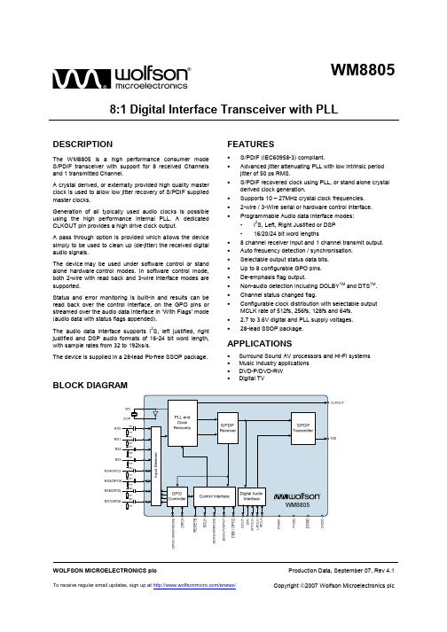
wWM88058:1 Digital Interface Transceiver with PLLWOLFSON MICROELECTRONICS plcProduction Data, September 07, Rev 4.1 DESCRIPTIONThe WM8805 is a high performance consumer mode S/PDIF transceiver with support for 8 received Channels and 1 transmitted Channel.A crystal derived, or externally provided high quality master clock is used to allow low jitter recovery of S/PDIF supplied master clocks.Generation of all typically used audio clocks is possible using the high performance internal PLL. A dedicated CLKOUT pin provides a high drive clock output.A pass through option is provided which allows the device simply to be used to clean up (de-jitter) the received digital audio signals.The device may be used under software control or stand alone hardware control modes. In software control mode, both 2-wire with read back and 3-wire interface modes aresupported.Status and error monitoring is built-in and results can be read back over the control interface, on the GPO pins or streamed over the audio data interface in ‘With Flags’ mode (audio data with status flags appended).The audio data interface supports I 2S, left justified, right justified and DSP audio formats of 16-24 bit word length, with sample rates from 32 to 192ks/s.The device is supplied in a 28-lead Pb-free SSOP package.BLOCK DIAGRAMFEATURES• S/PDIF (IEC60958-3) compliant.• Advanced jitter attenuating PLL with low intrinsic period jitter of 50 ps RMS.• S/PDIF recovered clock using PLL, or stand alone crystal derived clock generation.• Supports 10 – 27MHz crystal clock frequencies. • 2-wire / 3-Wire serial or hardware control interface. •Programmable Audio data interface modes: - I 2S, Left, Right Justified or DSP - 16/20/24 bit word lengths• 8 channel receiver input and 1 channel transmit output. • Auto frequency detection / synchronisation. •Selectable output status data bits.• Up to 8 configurable GPO pins. • De-emphasis flag output.• Non-audio detection including DOLBY TM and DTS TM . • Channel status changed flag.•Configurable clock distribution with selectable output MCLK rate of 512fs, 256fs, 128fs and 64fs. • 2.7 to 3.6V digital and PLL supply voltages. • 28-lead SSOP package. APPLICATIONS• Surround Sound AV processors and Hi-Fi systems • Music industry applications • DVD-P/DVD-RW• Digital TVWM8805Production DataTABLE OF CONTENTS DESCRIPTION (1)BLOCK DIAGRAM (1)FEATURES (1)APPLICATIONS (1)TABLE OF CONTENTS (2)PIN CONFIGURATION (3)ORDERING INFORMATION (3)PIN DESCRIPTION (4)ABSOLUTE MAXIMUM RATINGS (5)RECOMMENDED OPERATING CONDITIONS (6)SUPPLY CURRENT (6)ELECTRICAL CHARACTERISTICS (6)MASTER CLOCK TIMING (7)DIGITAL AUDIO INTERFACE – MASTER MODE (7)DIGITAL AUDIO INTERFACE – SLAVE MODE (8)CONTROL INTERFACE – 3-WIRE MODE (9)CONTROL INTERFACE – 2-WIRE MODE (10)DEVICE DESCRIPTION (11)INTRODUCTION (11)POWER UP CONFIGURATION (12)HARDWARE CONTROL MODE (18)DIGITAL ROUTING CONTROL (20)MASTER CLOCK AND PHASE LOCKED LOOP (21)SOFTWARE MODE INTERNAL CLOCKING (21)HARDWARE MODE INTERNAL CLOCKING (30)S/PDIF TRANSMITTER (31)S/PDIF RECEIVER (34)GENERAL PURPOSE OUTPUT (GPO) CONFIGURATION (44)DIGITAL AUDIO INTERFACE (45)AUDIO DATA FORMATS (46)REGISTER MAP (53)APPLICATIONS INFORMATION (63)RECOMMENDED EXTERNAL COMPONENTS (63)PACKAGE DIMENSIONS (64)IMPORTANT NOTICE (65)ADDRESS: (65)w PD Rev 4.1 September 07Production Data WM8805wPD Rev 4.1 September 07PIN CONFIGURATION( Top View )ORDERING INFORMATIONDEVICE TEMPERATURERANGE PACKAGE MOISTURESENSITIVITY LEVELPEAK SOLDERING TEMPERATUREWM8805GEDS -25 to +85oC 28-lead SSOP (Pb-free) MSL1 260o C WM8805GEDS/R -25 to +85o C28-lead SSOP (Pb-free, tape and reel)MSL1260o CNote:Reel quantity = 2,000WM8805Production DatawPD Rev 4.1 September 07PIN DESCRIPTIONPIN NAME Type DESCRIPTION1 DVDD Supply Digital core supply2 RX1 Digital In S/PDIF receive channel 13 RX0 Digital In S/PDIF receive channel 04 SCLKDigital In/Out Control interface clock / TRANS_ERR flag in hardware control mode. See note 2.5 GPO0 / SWIFMODEDigital In/Out General purpose digital output or selected functionality at hardware reset. See note 2.6 GPO1 Digital Out General purpose digital output7 SDIN / HWMODE Digital Input Control interface data input and hardware/software mode select at hardware reset. See note 2.8 SDOUT / GPO7 Digital In/Out Control interface data output / NON_AUDIO flag in hardware control mode / GPO in 2-wire software control mode. See note 2.9 CSB / GPO2 Digital In/Out Chip select / UNLOCK flag in hardware control mode / GPO in 2-wire software control mode. See note 2. 10 RESETB Digital Input System reset (active low) 11 PVDD Supply PLL core supply12 PGND Supply PLL ground 13CLKOUTDigital OutHigh drive clock output at 64fs, 128fs, 256fs and 512fs14 XOP Digital Output Crystal output 15 XIN Digital Input Crystal input 16 DOUT Digital Out Audio interface data output 17 DIN Digital In Audio interface data input 18 BCLK Digital In/Out Audio interface bit clock19 LRCLK Digital In/Out Audio interface left/right word clock 20 MCLK Digital In/Out Master clock input or output 21 TX0 Digital Out S/PDIF transmit22 RX7 / GPO6 Digital In/Out S/PDIF receive channel 7 or general purpose digital output 23 RX6 / GPO5 Digital In/Out S/PDIF receive channel 6 or general purpose digital output 24 RX5 / GPO4 Digital In/Out S/PDIF receive channel 5 or general purpose digital output 25 RX4 / GPO3Digital In/Out S/PDIF receive channel 4 or general purpose digital output 26 RX3 Digital In S/PDIF receive channel 3 27 RX2Digital InS/PDIF receive channel 228 DGND Supply Digital groundNotes : 1. Digital input pins have Schmitt trigger input buffers.2.Refer to Table 6 Device Configuration at Power up or Hardware ResetProduction Data WM8805wPD Rev 4.1 September 07ABSOLUTE MAXIMUM RATINGSAbsolute Maximum Ratings are stress ratings only. Permanent damage to the device may be caused by continuously operating at or beyond these limits. Device functional operating limits and guaranteed performance specifications are given under ElectricalCharacteristics at the test conditions specified.ESD Sensitive Device. This device is manufactured on a CMOS process. It is therefore generically susceptible to damage from excessive static voltages. Proper ESD precautions must be taken during handling and storage of this device.Wolfson tests its package types according to IPC/JEDEC J-STD-020B for Moisture Sensitivity to determine acceptable storage conditions prior to surface mount assembly. These levels are:MSL1 = unlimited floor life at <30°C / 85% Relative Humidity. Not normally stored in moisture barrier bag. MSL2 = out of bag storage for 1 year at <30°C / 60% Relative Humidity. Supplied in moisture barrier bag. MSL3 = out of bag storage for 168 hours at <30°C / 60% Relative Humidity. Supplied in moisture barrier bag. The Moisture Sensitivity Level for each package type is specified in Ordering Information. CONDITIONMIN MAX Digital core and I/O buffer supply voltage -0.3V +5V PLL supply voltage -0.3V +5V Voltage range digital inputs DGND -0.3VDVDD +0.3VMaster Clock Frequency 37MHz Operating temperature range, T A -25°C +85°C Storage temperature -65°C +150°CNote : 1. PLL and digital supplies must always be within 0.3V of each other. 2.PLL and digital grounds must always be within 0.3V of each other.WM8805Production DatawPD Rev 4.1 September 07RECOMMENDED OPERATING CONDITIONSPARAMETER SYMBOL TEST CONDITIONS MIN TYP MAX UNIT Digital supply range DVDD 2.7 3.6 V GroundDGND 0 V PLL supply range PVDD 2.7 3.6 VGround PGND0 VNote : 1. PLL and digital supplies must always be within 0.3V of each other. 2.PLL and digital grounds must always be within 0.3V of each other.SUPPLY CURRENTPARAMETER SYMBOL TEST CONDITIONS MIN TYP MAX UNIT Digital supply current I DVDD DVDD =3.3V 14.9 mA PLL supply current I PVDDPVDD = 3.3V 1.7 mAPower consumption DVDD/PVDD = 3.3V 54.8 mW Standby Power consumption DVDD/PVDD = 3.3V Device powered down0.11 mWELECTRICAL CHARACTERISTICSTest ConditionsPVDD = 3.3V, DVDD = 3.3V, PGND = 0V, DGND = 0V, T A = +25o C, fs = 48kHz, MCLK = 256fs unless stated. PARAMETER SYMBOL TEST CONDITIONS MIN TYP MAX UNIT Jitter Characteristics Intrinsic Period JitterJ i50 psDigital Logic Levels (CMOS Levels) Input LOW level V IL 0.3 x DVDD V Input HIGH level V IH 0.7 x DVDD V Output LOW V OL 0.1 x DVDD V Output HIGHV OH0.9 x DVDD VI source 25 mACLOCKOUT buffer drive capabilityI sinkCMOS 20pF load 25 mA S/PDIF Receiver Characteristics Input Resistance23 k ΩProduction DataWM8805wPD Rev 4.1 September 07MASTER CLOCK TIMINGFigure 1 Master Clock Timing RequirementsTest ConditionsPVDD = 3.3V, DVDD = 3.3V, PGND = 0V, DGND = 0V, T A = +25o C, fs = 48kHz, MCLK = 256fs unless stated.PARAMETER SYMBOL TEST CONDITIONS MIN TYP MAX UNIT System Clock Timing Information – Slave Mode MCLK System clock cycle time t MCLKY27nsMCLK System clock pulse width high t MCLKH 11 ns MCLK System clock pulse width low t MLCKL 11 ns MCLK Duty cycle40:60 60:40 %Table 1 Slave Mode MCLK Timing RequirementsDIGITAL AUDIO INTERFACE – MASTER MODEFigure 2 Digital Audio Data Timing – Master ModeTest ConditionsPVDD = 3.3V, DVDD = 3.3V, PGND = 0V, DGND = 0V, T A = +25o C, fs = 48kHz, MCLK = 256fs unless stated.PARAMETER SYMBOL TEST CONDITIONS MIN TYP MAX UNIT Audio Data Input Timing InformationLRCLK propagation delay from BCLK falling edget DL 0 10 ns DOUT propagation delay from BCLK falling edget DDA 0 10 ns DIN setup time to BCLK rising edget DST 10 ns DIN hold time from BCLK rising edget DHT10 nsTable 2 Digital Audio Data Timing – Master ModeWM8805Production DatawPD Rev 4.1 September 07DIGITAL AUDIO INTERFACE – SLAVE MODEFigure 3 Digital Audio Data Timing – Slave ModeTest ConditionsPVDD = 3.3V, DVDD = 3.3V, PGND = 0V, DGND = 0V, T A = +25o C, fs = 48kHz, MCLK = 256fs unless stated.PARAMETER SYMBOL TEST CONDITIONS MIN TYP MAX UNIT Audio Data Input Timing InformationBCLK cycle time t BCY 50 ns BCLK pulse width high t BCH 20 ns BCLK pulse width low t BCL 20 ns LRCLK set-up time to BCLK rising edget LRSU 10 ns LRCLK hold time from BCLK rising edge t LRH 10 ns DIN set-up time to BCLK rising edget DS 10 ns DIN hold time from BCLK rising edget DH 10 ns DOUT propagation delay from BCLK falling edget DD0 10 nsTable 3 Digital Audio Data Timing – Slave ModeProduction DataWM8805wPD Rev 4.1 September 07CONTROL INTERFACE – 3-WIRE MODEFigure 4 Control Interface Timing – 3-Wire Serial Control ModeTest ConditionsPVDD = 3.3V, DVDD = 3.3V, PGND = 0V, DGND = 0V, T A = +25o C, fs = 48kHz, MCLK = 256fs unless stated. PARAMETER SYMBOL MIN TYP MAX UNITProgram Register Input Information SCLK rising edge to CSB rising edge t SCS 60 ns SCLK cycle time t SCY 80 nsSCLK duty cycle40/60 60/40 %SDIN to SCLK set-up timet DSU 20 ns SDIN hold time from SCLK rising edget DHO 20 ns SDOUT propagation delay from SCLK rising edge t DL 5 ns CSB pulse width hight CSH 20 ns CSB rising/falling to SCLK rising t CSS 20 ns SCLK glitch suppressiont ps 2 8 nsTable 4 Control Interface Timing – 3-Wire Serial Control ModeWM8805Production DatawPD Rev 4.1 September 07CONTROL INTERFACE – 2-WIRE MODEFigure 5 Control Interface Timing – 2-Wire Serial Control ModeTest ConditionsPVDD = 3.3V, DVDD = 3.3V, PGND = 0V, DGND = 0V, T A = +25o C, fs = 48kHz, MCLK = 256fs unless stated. PARAMETER SYMBOL MIN TYP MAX UNITProgram Register Input Information SCLK cycle time t SCY 2500 nsSCLK duty cycle 40/60 60/40 %SCLK frequency400 kHz Hold Time (Start Condition) t STHO 600 ns Setup Time (Start Condition) t STSU 600 ns Data Setup Time t DSU 100 nsSDIN, SCLK Rise Time 300 nsSDIN, SCLK Fall Time 300 nsSetup Time (Stop Condition) t STOP 600 ns Data Hold Time t DHO 900 ns SCLK glitch suppressiont ps 2 8 nsTable 5 Control Interface Timing – 2-Wire Serial Control ModeDEVICE DESCRIPTIONINTRODUCTIONFEATURES•IEC-60958-3 compatible with 32 to 192k frames/s support.AES-3 data frames.• Supports•Support for reception and transmission of S/PDIF data.•Clock synthesis PLL with reference clock input and low jitter output.•Supports input reference clock frequencies from 10MHz to 27MHz.•Dedicated high drive clock output pin.•Register controlled channel status bit configuration.•Register read-back of recovered channel status bits and error flags.•Detection of non-audio data, sample rate and de-emphasis.•Programmable GPOs for error flags and frame status flags.The WM8805 is an IEC-60958 compatible S/PDIF transceiver with support for up to eight receivedS/PDIF data streams and one transmitted S/PDIF data stream.The receiver performs data and clock recovery, and transmits recovered data from the chip eitherthrough the digital audio interface or, alternatively, the device can loop the received S/PDIF databack out through the S/PDIF transmitter producing a de-jittered S/PDIF transmit data stream. Therecovered clock may be routed to a high drive output pin for external use. If there is no S/PDIF inputdata stream the PLL can be configured to output all standard MCLK frequencies or it can beconfigured to maintain the frequency of the last received S/PDIF data stream.The transmitter generates S/PDIF frames where audio data may be sourced from the S/PDIFreceiver or the digital audio interface. Timing for the S/PDIF transmitter interface can be sourcedfrom the internally derived MCLK in loop through mode or it can be taken from an external source.S/PDIF FORMATS/PDIF is a serial, bi-phase-mark encoded data stream. An S/PDIF frame consists of two sub-frames. Each sub-frame is made up of:•Preamble – a synchronization pattern used to identify the start of a 192-frame block or sub-frame•4-bit Auxiliary Data (AUX) – ordered LSB to MSB•20-bit Audio Data (24-bit when combined with AUX) – ordered LSB to MSB•Validity Bit – a 1 indicates invalid data in the associated sub-frame•User Bit – over 192-frames, this forms a User Data Block•Channel Bit – over 192-frames, this forms a Channel Status Block•Parity Bit – used to maintain even parity over the sub-frame (not including the preamble)An S/PDIF Block consists of 192 frames. Channel and user blocks are incorporated within the 192-frame S/PDIF Block. For Consumer mode only the first 40-frames are used to make up the Channeland User blocks. Figure 6 illustrates the S/PDIF format. The WM8805 does not support transmissionof user channel data. Received user channel data may be accessed via GPO pins.w PD Rev 4.1 September 07wPD Rev 4.1 September 07Figure 6 S/PDIF FormatPOWER UP CONFIGURATIONThe operating mode of the WM8805 is dependent upon the state of SDIN, SCLK, SDOUT, CSB and GPO0 when the device is powered up or a hardware reset occurs. Table 6 summarises the configuration options.HW RESET = 0HW RESET = 1SWMODE HWMODE SWMODE HWMODESDIN HWMODE / SWMODE SelectSDINN/ASCLKN/A AIF_MS SCLKGPO(TRANS_ERR)2-wire 3-wire SDOUTN/A AIF_CONF[0]GPO SDOUT GPO(NON_AUDIO)2-wire 3-wire2-wire 3-wireCSBDevice AddressN/ATXSRCGPO CSB GPO(UNLOCK)P I NGPO02-wire/3-wireMode SelectAIF_CONF[1] GPOGPO(GEN_FLAG)Note: AIF_CONF[1:0] configures the audio interface when the device operates in hardware mode. Refer to Table 16 for description of modes.Table 6 Device Configuration at Power up or Hardware ResetwPD Rev 4.1 September 07When the device powers up, all power up configuration pins are configured as inputs for a minimum of 9.4us and a maximum of 25.6us following the release of the external reset. The times are based on 27MHz and 10MHz crystal clock frequencies respectively. This enables the pins to be sampled and the device to be configured before the pins are released to their selected operating conditions. Figure 7 illustrates how SDIN is sampled.Figure 7 Pin Sampling On Power Up or Hardware ResetIf the device is powered up in Software control mode, all functions of the device are powered down by default and must be powered up individually by writing to the relevant bits of the PWRDN register (Table 7). In Hardware Control Mode, all functions of the device are powered up by default. REGISTER ADDRESSBITLABELDEFAULTDESCRIPTION0 PLLPD1 PLL Powerdown0 = PLL enabled 1 = PLL disabled 1 SPDIFRXPD 1S/PDIF Receiver Powerdown 0 = S/PDIF receiver enabled 1 = S/PDIF receiver disabled 2 SPDIFTXPD1S/PDIF Transmitter Powerdown0 = S/PDIF transmitter enabled 1 = S/PDIF transmitter disabled3 OSCPD0 Oscillator Power Down0 = Power Up 1 = Power Down 4 AIFPD0 Digital Audio Interface PowerDown0 = Power Up 1= Power Down R30 PWRDN 1Eh5 TRIOP0 Tri-state all Outputs0 = Outputs not tri-stated 1 = Outputs tri-statedTable 7 Power Down RegisterCONTROL INTERFACE OPERATIONControl of the WM8805 is implemented in either hardware control mode or software control mode.The method of control is determined by sampling the state of the SDIN/HWMODE pin at power up orat a hardware reset. If SDIN/HWMODE is low during power up the device is configured in hardwarecontrol mode, otherwise the device is configured in software control mode.SDIN/HWMODEmode0 Hardwaremode1 SoftwareTable 8 Hardware or Software Mode SelectSoftware control is achieved using a 3-wire (3-wire write, 4-wire read) or a 2-wire serial interface.The serial interface format is configured by sampling the state of the GPO0/SWIFMODE pin onpower up or at a hardware reset. If the GPO0/SWIFMODE pin is low the interface is configured in 2-wire mode, otherwise the interface is configured in 3-wire SPI compatible mode.GPO0/SWIFMODEinterface0 2-wireinterface1 3-wireTable 9 Software Mode Control Interface Select3-WIRE (SPI COMPATIBLE) SERIAL CONTROL MODE – REGISTER WRITESDIN is used for the program data, SCLK is used to clock in the program data and CSB is used tolatch in the program data. SDIN is sampled on the rising edge of SCLK. The 3-wire interface writeprotocol is shown in Figure 8.Figure 8 3-Wire Serial Interface Register Write Protocol•W is a control bit indicating a read or write operation. 0 =write operation, 1 = read operation•REGA[6:0] is the register Address.•DIN[7:0] is the data to be written to the register being addressed.•CSB is edge sensitive – the data is latched on the rising edge of CSB.w PD Rev 4.1 September 073-WIRE SERIAL CONTROL MODE REGISTER READ-BACKNot all registers can be read. Only the device ID (registers R0, R1 and R2) and the status registers can be read. These status registers are labelled as “read only” in the Register Map section.The read-only status registers can be read back via the SDOUT pin. The registers can be read by one of two methods, selected by the CONT register bit and the ‘W’ control bit. The oscillator must be powered up before 3-wire control interface read-back is possible.When CONT =1 and ‘W’=0, a single read-only register can be read back by writing to any other register or to a dummy register. The register to be read is determined by the READMUX[2:0] bits. When a write to the device is performed, the device will respond by returning the status byte of the register selected by the READMUX register bits. The data is returned on the SDOUT pin. This 3-wire interface read-back method using a write access is shown in Figure 9.REGISTER ADDRESS BIT LABEL DEFAULT DESCRIPTION2:0 READMUX[2:0] 000 Status Register SelectDetermines which status registeris to be read back:000 = Interrupt Status Register001 = Channel Status Register 1010 = Channel Status Register 2011 = Channel Status Register 3100 = Channel Status Register 4101 = Channel Status Register 5110 = S/PDIF Status RegisterR29SPDRX11Dh3 CONT 0 Continuous Read Enable0 = Continuous read-back modedisabled1 = Continuous read-back modeenabledTable 10 Read-back Control RegisterThe SDOUT pin is tri-state unless CSB is held low; therefore CSB must be held low for the durationof the read.Figure 9 3-Wire Control Interface Read-Back Method 1The second method of reading the read only status registers is If CONT=0 and ‘W’=1. Using thismethod the user can read back directly from a register by reading the register address. The devicewill respond with the contents of the register. The protocol for this read-back method is shown inFigure 10.w PD Rev 4.1 September 07wPD Rev 4.1 September 07Figure 10 3-Wire Control Interface Read-Back Method 22-WIRE SERIAL CONTROL WITH READ-BACK MODEThe WM8805 supports software control via a 2-wire serial bus. Many devices can be controlled by the same bus and each device has a unique 7-bit address (see Table 11).The controller indicates the start of data transfer with a high to low transition on SDIN while SCLK remains high. This indicates that a device address, DEVA(7:1), and data, REG(6:0), will follow. All devices on the 2-wire bus will shift in the next eight bits on SDIN (7-bit address DEVA(7:1), + read/write ‘W’ bit, MSB first). If the device address received matches the address of the WM8805, the WM8805 responds by driving SDIN low on the next clock pulse (ACK). This is a device acknowledgement of an address match. If the address does not match that of the WM8805, the device returns to the idle condition and waits for a new start condition and valid address.Once the WM8805 has acknowledged a matching address, the controller sends the first byte of control data, which is the WM8805 register address (REGA[6:0]). The WM8805 then acknowledges reception of the control data byte by pulling SDIN low for one clock pulse (another ACK). The controller then sends the second byte of control data (DIN[7:0], i.e. the eight bits of register data to be written), and the WM8805 acknowledges again by pulling SDIN low (another ACK).The transfer of data is complete when there is a low to high transition on SDIN while SCLK is high. After receiving a complete address and data sequence the WM8805 returns to the idle state and waits for another start condition. If a start or stop condition is detected out of sequence at any pointduring data transfer (i.e. SDIN changes while SCLK is high), the device returns to the idle condition.Figure 11 2-Wire Serial Control Interface WriteMultiple consecutive register writes can be performed in 2-wire control mode by setting the CONT bit high. This method allows the entire register map to be defined in a one continuous write operation.wPD Rev 4.1 September 07Figure 12 2-Wire Serial Control Interface Multi-WriteThe WM8805 has two possible device addresses, which can be selected using the CSB pin during hardware reset.CSB STATEDEVICE ADDRESS IN2-WIRE MODEADDRESS (X=R/W BIT)X=0 X= 1 Low0111010x0x7A0x75High 0111011x 0x76 0x77Table 11 2-Wire Interface Address Selection2-WIRE SERIAL CONTROL MODE -REGISTER READ-BACKThe WM8805 allows read-back of certain registers in 2-wire mode. The protocol is similar to thatused to write to the device. The controller will issue the device address followed by a write bit, the register index will then be passed to the WM8805. At this point the controller will issue a repeated start condition and resend the device address along with a read bit. The WM8805 will acknowledge this and the WM8805 will become a slave transmitter. The WM8805 will transmit the data from the indexed register on SDIN MSB first. When the controller receives the data it will not acknowledge receipt of the data indicating that it will resume master transmitter control of SDIN. The controller willthen issue a stop command completing the read cycle. Figure 13 illustrates the read protocol.Figure 13 2-Wire Serial Control Interface Read (CONT=0)2-WIRE SERIAL CONTROL MODE – CONTINUOUS READ-BACKAs in 3-wire mode, there are two methods of reading back data: continuous and non-continuous read-back. Continuous read-back is selected by setting CONT to 1. In continuous read-back mode, the device will return the indexed register first followed by consecutive registers in increasing index order until the controller does not acknowledge the data then issues a stop sequence. This is shownin Figure 14Figure 14 2-Wire Serial Interface Continuous Read-Back (CONT=1)wPD Rev 4.1 September 07SOFTWARE REGISTER RESETWriting to register 0000000 will reset the WM8805. This will reset all register bits to their default values. Note that the WM8805 is powered down by default so writing to this register will power down the device.DEVICE ID AND REVISION IDENTIFICATIONRegisters 0,1 and 2 can be read to identify the device ID and IC revision number. Refer to Table 12 for details.REGISTER ADDRESS BIT LABEL DEFAULTDESCRIPTIONRESET N/A Writing to this register will apply a reset to the device. R00RST/DEVID100h7:0DEVID1[7:0] 00000101 Reading from this register will returnthe second part of the device ID00000101 = 0x05 R01 DEVID2 01h (read only) 7:0DEVID2[7:0] 10001000 Reading from this register will returnthe first part of the device ID10001000 = 0x88 R02 DEVREV 02h3:0 DEVREV [3:0]N/AReading from this register will return the device revision. 0x1 = revision 1Table 12 Software Reset Register and Device IDHARDWARE CONTROL MODEThe WM8805 can be operated in either software or hardware control modes. The method of control is determined by sampling the state of the SDIN pin during power up or hard reset. If SDIN is LOW during power up or hardware reset, the WM8805 will be switched into hardware control mode.PIN 0 1SDINHardware Control ModeSoftware Control ModeTable 13 Hardware / Software Mode ConfigurationIn hardware control mode the user has limited control over the configuration of the device. Most of the features will assume default values but some can be configured using external pins. When the device is configured in hardware control mode, all functions of the device are powered up.The clock and data recovery module with the WM8805 will require a 12 MHz crystal derived master clock as the default values for this module cannot be altered in Hardware Control mode.MASTER / SLAVE MODE SELECTIONThe WM8805 can be configured in either master or slave mode In software control mode this is set by writing to AIF_MS in the AIFRX register. In hardware control mode this is controlled by sampling the SCLK pin on power up or hardware reset. PIN(HARDWARE MODE)REGISTER (SOFTWARE MODE) 0 1SCLKAIF_MSSlave Mode Master ModeTable 14 Master / Slave Mode Configuration in Hardware ModeDIGITAL ROUTING CONTROLSee page 20 for a full description of the signal routing options available in the WM8805. In Software control mode the values set in registers TXSRC and RXINSEL determine the S/PDIF Rx data source and destination. In hardware control mode the device can receive data only from RX0 but can set the value of TXSRC directly using the CSB pin. This determines the S/PDIF transmitter data sourcePIN (HARDWARE MODE)REGISTER(SOFTWAREMODE)0 1CSB TXSRC S/PDIFRxAIFRxTable 15 S/PDIF Transmitter Digital Routing Control ConfigurationAUDIO INTERFACE CONTROLIn software control mode the audio data word length and audio data format can be set independently for the receiver and transmitter sides of the interface. However, in hardware control mode both sides of the interface are combined and the configuration is set using SDOUT and GPO0 pins as described in Table 6 and Table 16. Note that AIF_CONF[1:0] configures the audio interface when the device operates in hardware mode.GPO0 / AIFCONF[1]SDOUT /AIFCONF[0]DESCRIPTION0 0 16-bitI2S0 1 24-bitI2S1 0 24-bit Left Justified With Flags1 1 16-bitRightJustifiedTable 16 Digital Audio Interface Control in Hardware Control ModeSTATUS INFORMATIONIn hardware control mode the WM8805 outputs a selection of status flags for the user. Table 17describes the flags which are available and the output pins on which they are available.PIN STATUSFLAGSCLK TRANS_ERRSDOUT NON_AUDIOCSB UNLOCKGPO0 GEN_FLAGTable 17 Hardware Control Mode Status Flag ConfigurationA full description of the status flags is given in Table 45.w PD Rev 4.1 September 07。
WM_W800_入门手册说明书
WM_W800_入门手册V1.2北京联盛德微电子有限责任公司(winner micro)地址:北京市海淀区阜成路67号银都大厦1802电话:+86-10-62161900公司网址:文档修改记录版本修订时间修订记录作者审核V0.12019/9/25[C]创建文档CuiycV0.22020/6/12增加cygwin编译环境CuiycV0.32020/7/8统一字体CuiycV1.02020/8/4添加硬件开发板CuiycV1.12020/11/5更新高速接口介绍RayCuiycV1.22021/2/4推荐使用IDE为CDK,不再维护CDS的工程目录文档修改记录 (2)目录 (3)1概述 (5)2准备工作 (5)3w800开发板简介 (6)4w800编译环境搭建 (7)4.1w800工具链 (7)4.2开发环境安装 (7)4.2.1Windows (7)4.2.2Linux (9)4.2.3Mac OS (10)5SDK工程获取 (10)6SDK工程编译 (10)6.1Windows (10)6.1.1Ubuntu虚拟机 (10)6.2Linux (11)6.3mac os (11)7固件烧录 (11)7.1Window下的操作步骤 (11)7.2Linux下升级步骤 (15)7.3Mac os下升级步骤 (15)8串口调试 (15)9w800 sdk如何开始编写用户程序 (15)9.1用户入口 (15)9.2demo如何使用 (16)9.3at指令如何使用 (16)1概述指导如何用户搭建w800硬件开发的软件环境,通过示例工程展示如何编译、下载固件到w800开发板等操作步骤。
该手册基于W800的ARDUINO开发板进行介绍及示例的升级运行。
w800是一款基于XT804内核SoC,支持功能:⚫ 2.4G Wi-Fi⚫蓝牙⚫内置多种数字接口(QFlash,外扩PSRAM,UART,GPIO,I²C,PWM,I²S,7816,SDIO,HSPI,TouchSensor)⚫支持多种硬件加解密算法(RC4,DES,3DES,AES,RSA,MD5,SHA1)⚫内置安全功能2准备工作硬件:⚫w800开发板⚫USB数据线(Micro USB)⚫PC(Windows、linux或Mac OS)软件:⚫工具链,用于编译w800代码⚫编译工具⚫w800 sdk⚫串口工具(支持xmodem协议)⚫代码编辑器3w800开发板简介W800 Arduino开发板,提供了如下接口:⚫I2C&I2S接口⚫Uart0&SWD调试接口⚫SPI&Uart1通信接口⚫PWM接口⚫SIM 接口⚫GPIO⚫Micro USB 接口用户通过Micro USB口与上位机相连,通过UART0口进行固件烧录。
WM8978中文资料
描述 ........................................................................ 3 产品特征 .................................................................... 3
1
输入限幅器/电平自动控制(ALC)..................................... 25 ALC 芯片保护 .......................................................29 噪声门............................................................. 29 输出信号线路....................................................... 30 数字重放(DAC)线路................................................ 30 数字 Hi-Fi DAC 音量(增益)控制.....................................31 DAC 5 路均衡器 .....................................................32 DAC 3D 放大 ........................................................32 音量推动........................................................... 32 5 路图表均衡器 .....................................................34 3D 立体声放大 ......................................................36 模拟输出........................................................... 36 左和右通道混合器................................................... 36 耳机输出(LOUT1 和 ROUT1)..........................................39 扬声器输出(LOUT2 和 ROUT2)........................................41 零交叉间歇时间..................................................... 44 OUT3/OUT4 混合和输出 ...............................................44 输出使能........................................................... 48 过热保护........................................................... 48 未使用的模拟输入/输出.............................................. 48 数字音频接口....................................................... 51 主属和从属操作模式................................................. 51 音频数据模式....................................................... 51 音频接口控制....................................................... 54 环回............................................................... 54 压缩............................................................... 54 音频采样率......................................................... 55 主时钟和锁相环(PLL).............................................. 56 通用的输入/输出.................................................... 57 输出开关选择(插座检测)........................................... 58 控制接口........................................................... 59 控制模式选择和 2 线模式地址.........................................59 3 线串行控制模式 ...................................................59 2 线串行控制模式 ...................................................59 芯片复位........................................................... 60 电源............................................................... 60 推荐的上电/断电顺序................................................ 60 电源管理........................................................... 61 通过减少过采样率节省电能........................................... 61 VMID............................................................... 61 BIASEN............................................................. 61 源电流估算......................................................... 61
897说明书

前面板控制钮及开关1 液晶显示屏液晶显示屏(lcd)用来显示工作频率及电台的其它工作状况 2 func(功能)键这三个键用来选择很多最重要的电台操作特性。
按一下[f]键,然后旋转mem/v of ch旋钮,相应的功能键就[a)[b][c]三个键的上方(在lcd的底部),通过这三个键可以选择17组功能。
3 mic插座将配套的mh-31手持话筒插在这个插座中4 phone插口这个1/4英寸,3接点的插座用来连接单声道或立体声的耳机。
耳机插入后,主机扬声器就静音了。
耳机音量用af钮来调整。
5 电源开关按住这个开关1秒钟,就可以开启或关闭电台电源。
电源开启时,轻按一下这个键,就可以调整频率调谐的速度,在快速调谐状态下,屏幕右下角会出现一个跑步者的图形6 [f]键按一下这个键后可以通过旋转mem/vfo ch旋钮来改变多功能键([a],[b][c])的功能按住这个键一秒钟则可以激活相应的菜单模式。
7 lock键按一下这个键可以锁住前面板上的功能按键/旋钮,以防止无意间改变工作频率。
8 主旋钮dial这是电台的主要调谐旋钮。
可以用来调节频率以及“菜单”中的各项设置。
9 af旋钮这个旋钮是复合钮的内圈,用来调节内置扬声器或外接喇叭的音量。
顺时针为加大音量10 sql/rf旋钮这个旋钮是复合旋钮的外围,用来调节接收时射频及中频的电平,也可以通过菜单模式no-08c [sql/rf gain)的设置,用来调节静噪水平。
出厂时的缺省设置就是静噪调节状态。
11 clar/if shift键按动这个键可以激活接收信号时的清音功能。
这个功能是用来调节最大±9.99khz的频偏。
发射频率不受这个调节的影响。
按住这个键一秒钟就激活了if(中频)频偏功能,用来调节中频滤波器的频带中心频率。
12 clar旋钮当按一下clar/if shift钮以后,旋转clar旋钮就可以在±9.99khz的范围内调节清音器13 band(dwn)/band(up)按键这两个键是用来向上(up)或向下(dwn)移动频带的,可以选择的频带顺序如下:14 mem/vfo ch旋钮这个旋钮可以用来调节工作频率、存储信道以及[a],[b],[c]功能选择。
WM8974_07资料

wWM8974Mono CODEC with Speaker DriverWOLFSON MICROELECTRONICS plc Production Data, Rev 4.2 March 2007DESCRIPTIONThe WM8974 is a low power, high quality mono CODEC designed for portable applications such as Digital Still Camera or Digital Voice Recorder.The device integrates support for a differential or single ended mic, and includes drivers for speakers or headphone, and mono line output. External component requirements are reduced as no separate microphone or headphone amplifiers are required.Advanced Sigma Delta Converters are used along with digital decimation and interpolation filters to give high quality audio at sample rates from 8 to 48ks/s. Additional digital filtering options are available in the ADC path, to cater for application filtering such as ‘wind noise reduction’, plus an advanced mixed signal ALC function with noise gate is provided. The digital audio interface supports A-law and µ-law companding. An on-chip PLL is provided to generate the required Master Clock from an external reference clock. The PLL clock can also be output if required elsewhere in the system.The WM8974 operates at supply voltages from 2.5 to 3.6V, although the digital supplies can operate at voltages down to 1.71V to save power. The speaker and mono outputs use a separate supply of up to 5V which enables increased output power if required. Different sections of the chip can also be powered down under software control by way of the selectable two or three wire control interface.WM8974 is supplied in a very small 4x4mm QFN package, offering high levels of functionality in minimum board area, with high thermal performance.FEATURES• Mono CODEC:• Audio sample rates:8, 11.025, 16, 22.05, 24, 32, 44.1, 48kHz • DAC SNR 98dB, THD -84dB (‘A’-weighted @ 8 – 48ks/s) • ADC SNR 94dB, THD -83dB (‘A’-weighted @ 8 – 48ks/s) • On-chip Headphone/Speaker Driver with ‘cap-less’ connect - 40mW output power into 16Ω / 3.3V SPKVDD - BTL speaker drive 0.9W into 8Ω / 5V SPKVDD • Additional MONO Line output• Multiple analog or ‘Aux’ inputs, plus analog bypass path • Mic Preamps:•Differential or single end Microphone Interface - Programmable preamp gain- Psuedo differential inputs with common mode rejection - Programmable ALC / Noise Gate in ADC path •Low-noise bias supplied for electret microphonesOTHER FEATURES• 5 band EQ (record or playback path) • Digital Playback Limiter• Programmable ADC High Pass Filter (wind noise reduction) • Programmable ADC Notch Filter • On-chip PLL• Low power, low voltage- 2.5V to 3.6V (digital: 1.71V to 3.6V)- power consumption <10mA all-on 48ks/s mode • 4x4x0.9mm 24 lead QFN packageAPPLICATIONS• Digital Still Camera Audio Codec• Wireless VoIP and other communication device handsets / headsets• Portable audio recorder•General Purpose low power audio CODECWM8974Production DataTABLE OF CONTENTS DESCRIPTION (1)FEATURES (1)APPLICATIONS (1)TABLE OF CONTENTS (2)PIN CONFIGURATION (3)ORDERING INFORMATION (3)PIN DESCRIPTION (4)ABSOLUTE MAXIMUM RATINGS (5)RECOMMENDED OPERATING CONDITIONS (5)ELECTRICAL CHARACTERISTICS (6)TERMINOLOGY (8)SIGNAL TIMING REQUIREMENTS (9)SYSTEM CLOCK TIMING (9)AUDIO INTERFACE TIMING – MASTER MODE (9)AUDIO INTERFACE TIMING – SLAVE MODE (10)CONTROL INTERFACE TIMING – 3-WIRE MODE (11)CONTROL INTERFACE TIMING – 2-WIRE MODE (12)DEVICE DESCRIPTION (13)INTRODUCTION (13)INPUT SIGNAL PATH (14)ANALOGUE TO DIGITAL CONVERTER (ADC) (19)INPUT LIMITER / AUTOMATIC LEVEL CONTROL (ALC) (23)OUTPUT SIGNAL PATH (35)ANALOGUE OUTPUTS (42)OUTPUT SWITCH (47)DIGITAL AUDIO INTERFACES (49)AUDIO SAMPLE RATES (54)MASTER CLOCK AND PHASE LOCKED LOOP (PLL) (55)GENERAL PURPOSE INPUT/OUTPUT (57)CONTROL INTERFACE (57)RESETTING THE CHIP (58)POWER SUPPLIES (58)POWER MANAGEMENT (63)REGISTER MAP (65)REGISTER BITS BY ADDRESS (66)DIGITAL FILTER CHARACTERISTICS (77)TERMINOLOGY (77)DAC FILTER RESPONSES (78)ADC FILTER RESPONSES (78)DE-EMPHASIS FILTER RESPONSES (79)HIGHPASS FILTER (80)5-BAND EQUALISER (81)APPLICATIONS INFORMATION (85)RECOMMENDED EXTERNAL COMPONENTS (85)PACKAGE DIAGRAM (86)IMPORTANT NOTICE (87)ADDRESS: (87)Production Data WM8974 PIN CONFIGURATIONTOPVIEWORDERING INFORMATIONORDER CODE TEMPERATURERANGE PACKAGE MOISTURESENSITIVITYLEVELPACKAGE BODYTEMPERATUREWM8974GEFL/V -25°C to +85°C 24-lead QFN (4x4x0.9mm)(Pb-free)MSL3 260o CWM8974GEFL/RV -25°C to +85°C 24-lead QFN (4x4x0.9mm)(Pb-free, tape and reel)MSL3 260o C Note:Reel Quantity = 3,500WM8974Production Data PIN DESCRIPTIONPIN NO NAME TYPE DESCRIPTION1 MICBIAS Analogue Output Microphone bias2 AVDD Supply Analogue supply (feeds ADC and DAC)3 AGND Supply Analogue ground (feeds ADC and DAC)4 DCVDD Supply Digital core supply5 DBVDD Supply Digital buffer (input/output) supplyground6 DGND Supply Digital7 ADCDAT Digital Output ADC digital audio data output8 DACDAT Digital Input DAC digital audio data input9 FRAME Digital Input / Output DAC and ADC sample rate clock or frame synch10 BCLK Digital Input / Output Digital audio port clock11 MCLK Digital Input Master clock input12 CSB/GPIO Digital Input / Output 3-Wire MPU chip select or general purpose input/output pin.13 SCLK Digital Input 3-Wire MPU clock Input / 2-Wire MPU Clock Input14 SDIN Digital Input / Output 3-Wire MPU data Input / 2-Wire MPU Data Input15 MODE Digital Input Control interface mode selection pin.Analogue Output Mono output16 MONOOUTAnalogue Output Speaker output positive17 SPKOUTPSupply Speaker ground (feeds speaker and mono output amps only)18 SPKGNDAnalogue Output Speaker output Negative19 SPKOUTNSupply Speaker supply (feeds speaker and mono output amps only)20 SPKVDDAnalogue Input Auxiliary analogue input21 AUXReference Decoupling for midrail reference voltage22 VMIDAnalogue Input Microphone negative input23 MICNAnalogue Input Microphone positive input (common mode)24 MICPNote:It is recommended that the QFN ground paddle should be connected to analogue ground on the application PCB.Production DataWM8974ABSOLUTE MAXIMUM RATINGSAbsolute Maximum Ratings are stress ratings only. Permanent damage to the device may be caused by continuouslyoperating at or beyond these limits. Device functional operating limits and guaranteed performance specifications are given under Electrical Characteristics at the test conditions specified.ESD Sensitive Device. This device is manufactured on a CMOS process. It is therefore generically susceptible to damage from excessive static voltages. Proper ESD precautions must be taken during handling and storage of this device.Wolfson tests its package types according to IPC/JEDEC J-STD-020B for Moisture Sensitivity to determine acceptable storage conditions prior to surface mount assembly. These levels are:MSL1 = unlimited floor life at <30°C / 85% Relative Humidity. Not normally stored in moisture barrier bag. MSL2 = out of bag storage for 1 year at <30°C / 60% Relative Humidity. Supplied in moisture barrier bag. MSL3 = out of bag storage for 168 hours at <30°C / 60% Relative Humidity. Supplied in moisture barrier bag. The Moisture Sensitivity Level for each package type is specified in Ordering Information. CONDITION MIN MAXDBVDD, DCVDD, AVDD supply voltages -0.3V +4.2 SPKVDD supply voltage -0.3V +7V Voltage range digital inputs DGND -0.3V DVDD +0.3V Voltage range analogue inputs AGND -0.3VAVDD +0.3VOperating temperature range, T A -25°C +85°CStorage temperature prior to soldering 30°C max / 85% RH max Storage temperature after soldering -65°C +150°CNotes 1. Analogue and digital grounds must always be within 0.3V of each other. 2. All digital and analogue supplies are completely independent from each other.RECOMMENDED OPERATING CONDITIONSPARAMETER SYMBOL TEST CONDITIONS MIN TYP MAX UNITDigital supply range (Core) DCVDD 1.71 3.6 VDigital supply range (Buffer) DBVDD 1.71 3.6 V Analogue supplies range AVDD 2.5 3.6 VSpeaker supply SPKVDD 2.5 5.5 VGround DGND,AGND,SPKGNDVNotes 1. When using PLL, DCVDD must be 1.9V or higher. 2. AVDD must be ≥ DCVDD.3. DBVDD must be ≥ DCVDD.4. In non-boosted mode, SPKVDD must be ≥ AVDD, if boosted SPKVDD must be ≥ 1.5x AVDD.5.When using PLL, DCVDD must be ≥ 1.9V.WM8974Production DataELECTRICAL CHARACTERISTICSTest ConditionsDCVDD = 1.8V, AVDD = DBVDD = 3.3V, SPKVDD = 3.3V, T A = +25o C, 1kHz signal, fs = 48kHz, 24-bit audio data unless otherwise stated.PARAMETER SYMBOL TEST CONDITIONS MIN TYP MAX UNIT Microphone Inputs (MICN, MICP) Full-scale Input Signal Level (Note 1) – note this changes with AVDDV INFSPGABOOST = 0dB INPPGAVOL = 0dB1.0 0 VrmsdBVMic PGA equivalent input noise At 35.25dBgain 150 uVInput resistance R MICIN Gain set to 35.25dB 1.6 k Ω Input resistance R MICIN Gain set to 0dB 47 k Ω Input resistance R MICIN Gain set to -12dB 75 k Ω Input resistance R MICIP MICP2INPPGA = 1 94 k Ω Input resistance R MICIP MICP2INPPGA = 094k ΩInput Capacitance C MICIN 10 pF MIC Input Programmable Gain Amplifier (PGA)Programmable Gain-12 35.25 dBProgrammable Gain Step Size Guaranteed monotonic0.75dBMute Attenuation 108 dB Selectable Input Gain Boost (0/+20dB)Gain Boost 0 20 dB Automatic Level Control (ALC)/Limiter – ADC onlyTarget Record Level -28.5 -6 dB Programmable Gain-12 35.25 dBProgrammable Gain Step Size Guaranteed Monotonic0.75dB Gain Hold Time (Note 2)t HOLD MCLK=12.288MHz (Note 4) 0, 2.67, 5.33, 10.67, … , 43691 (time doubles with each step) ms ALCMODE=0 (ALC), MCLK=12.288MHz(Note 4) 3.3, 6.6, 13.1, … , 3360 (time doubles with each step) Gain Ramp-Up (Decay) Time (Note 3)t DCYALCMODE=1 (limiter), MCLK=12.288MHz(Note 4)0.73, 1.45, 2.91, … , 744 (time doubles with each step) msALCMODE=0 (ALC), MCLK=12.288MHz(Note 4) 0.83, 1.66, 3.33, … , 852 (time doubles with each step) Gain Ramp-Down (Attack) Time (Note 3)t ATKALCMODE=1 (limiter), MCLK=12.288MHz(Note 4)0.18, 0.36, 0.73, … , 186 (time doubles with each step)msAnalogue to Digital Converter (ADC) Signal to Noise Ratio (Note 5) SNR A-weighted,0dB PGA gain 85 94 dB Total Harmonic Distortion (Note 6)THD-1dBFS input, 0dB PGA gain-75 -83 dBAuxilliary Analogue Input (AUX) Full-scale Input Signal Level (0dB) – note this changes with AVDD V INFS 1.0 0 VrmsdBVInput Resistance R AUXIN AUXMODE =0 20 k ΩInput Capacitance C AUXIN10 pFProduction DataWM8974Test ConditionsDCVDD = 1.8V, AVDD = DBVDD = 3.3V, SPKVDD = 3.3V, T A = +25o C, 1kHz signal, fs = 48kHz, 24-bit audio data unless otherwise stated.PARAMETER SYMBOL TEST CONDITIONS MIN TYP MAX UNIT Digital to Analogue Converter (DAC) to MONO output (all data measured with 10k Ω / 50pF load) Signal to Noise Ratio (Note 5) SNR A-weighted 90 98 dB Total Harmonic Distortion + Noise (Note 6)THD+N R L = 10 k Ωfull-scale signal-84 dBMONOBOOST =0 AVDD/3.30dB Full Scale output voltage (Note 9)MONOBOOST=11.5x(AVDD/3.3)V RMS Speaker Output PGA Programmable Gain-57 6 dBProgrammable Gain Step SizeGuaranteed monotonic1dBBTL Speaker Output (SPKOUTP, SPKOUTN with 8Ω bridge tied load)Output PowerP O Output power is very closely correlated with THD; see belowP O =180mW, R L = 8Ω,SPKVDD=3.3V 0.03 -70 % dB P O =400mW, R L = 8Ω,SPKVDD=3.3V 5.0 -26 % dB P O =360mW, R L = 8Ω,SPKVDD=5V 0.02 -75 % dB Total Harmonic Distortion + Noise (Note 6)THD+NP O =800mW, R L = 8Ω,SPKVDD=5V0.06 -65 % dB SPKVDD=3.3V,R L = 8Ω 90 101 dB Signal to Noise RatioSNRSPKVDD=5V, R L = 8Ω102 dBPower Supply Rejection Ratio50 dB‘Headphone’ output (SPKOUTP, SPKOUTN with resistive load to ground)Signal to Noise RatioSNR 100 dB Total Harmonic Distortion + Noise (Note 6) THD+N Po =20mW, R L = 16Ω,SPKVDD=3.3V0.02 -74 %dBPo=20mW, R L = 32Ω, SPKVDD=3.3V0.017 - 75 % dB Microphone Bias Bias Voltage (MBVSEL=0) V MICBIAS0.9*AVDDVBias Voltage (MBVSEL=1) V MICBIAS 0.65*AVDD V Bias Current Source I MICBIAS 3 mA Output Noise Voltage Vn1K to 20kHz15nV/√HzDigital Input / Output Input HIGH Level V IH 0.7×DVDD V Input LOW Level V IL 0.3×DVDD VOutput HIGH Level V OH I OL =1mA 0.9×DVDDVOutput LOW LevelV OLI OH -1mA 0.1xDVDD VWM8974Production Data TERMINOLOGY1. MICN input only in single ended microphone configuration. Maximum input signal to MICP without distortion is -3dBV.2. Hold Time is the length of time between a signal detected being too quiet and beginning to ramp up the gain. It doesnot apply to ramping down the gain when the signal is too loud, which happens without a delay.3. Ramp-up and Ramp-Down times are defined as the time it takes for the PGA to change it’s gain by 6dB.4. All hold, ramp-up and ramp-down times scale proportionally with MCLK5. Signal-to-noise ratio (dB) – SNR is a measure of the difference in level between the full scale output and the output withno signal applied. (No Auto-zero or Automute function is employed in achieving these results).6. THD+N (dB) – THD+N is a ratio, of the rms values, of (Noise + Distortion)/Signal.7. The maximum output voltage can be limited by the speaker power supply. If MONOBOOST=1 then SPKVDD shouldbe 1.5xAVDD or higher to prevent clipping taking place in the output stage.Production DataWM8974SIGNAL TIMING REQUIREMENTSSYSTEM CLOCK TIMINGFigure 1 System Clock Timing RequirementsTest ConditionsDCVDD=1.8V, DBVDD=AVDD=SPKVDD=3.3V, DGND=AGND=SPKGND=0V, T A = +25o CPARAMETER SYMBOL CONDITIONS MIN TYP MAX UNIT System Clock Timing Information MCLK=SYSCLK (=256fs)81.38ns MCLK cycle time T MCLKYMCLK input to PLL Note 1 20nsMCLK duty cycle T MCLKDS 60:40 40:60Note 1:PLL pre-scaling and PLL N and K values should be set appropriately so that SYSCLK is no greater than 12.288MHz.AUDIO INTERFACE TIMING – MASTER MODEFigure 2 Digital Audio Data Timing – Master Mode (see Control Interface)WM8974Production DataTest ConditionsDCVDD=1.8V, DBVDD=AVDD=SPKVDD=3.3V, DGND=AGND=SPKGND=0V, T A =+25o C, Master Mode, fs=48kHz, MCLK=256fs,24-bit data, unless otherwise stated. PARAMETER SYMBOL MIN TYP MAX UNITAudio Data Input Timing InformationFRAME propagation delay from BCLK falling edge t DL 10 ns ADCDAT propagation delay from BCLK falling edge t DDA 10 ns DACDAT setup time to BCLK rising edge t DST 10 ns DACDAT hold time from BCLK rising edge t DHT 10 nsNote:BCLK period should always be greater than MCLK period.AUDIO INTERFACE TIMING – SLAVE MODEFigure 3 Digital Audio Data Timing – Slave ModeTest ConditionsDCVDD=1.8V, DBVDD=AVDD=SPKVDD=3.3V, DGND=AGND=SPKGND=0V, T A =+25o C, Slave Mode, fs=48kHz, MCLK= 256fs, 24-bit data, unless otherwise stated.PARAMETER SYMBOL MIN TYP MAX UNIT Audio Data Input Timing InformationBCLK cycle time t BCY 160 ns BCLK pulse width high t BCH 64 ns BCLK pulse width lowt BCL 64 ns FRAME set-up time to BCLK rising edge t LRSU 10 ns FRAME hold time from BCLK rising edge t LRH 10 ns DACDAT hold time from BCLK rising edge t DH 10 ns DACDAT set-up time to BCLK rising edge t DS 10 ns ADCDAT propagation delay from BCLK falling edge t DD 20 nsCONTROL INTERFACE TIMING – 3-WIRE MODEFigure 4 Control Interface Timing – 3-Wire Serial Control ModeTest ConditionsDCVDD = 1.8V, DBVDD = AVDD = SPKVDD = 3.3V, DGND = AGND = SPKGND = 0V, T A = +25o C, Slave Mode, fs = 48kHz,MCLK = 256fs, 24-bit data, unless otherwise stated.UNITMAXTYPMINPARAMETER SYMBOLProgram Register Input InformationSCLK rising edge to CSB rising edge t SCS 80 nsSCLK pulse cycle time t SCY 200 nsSCLK pulse width low t SCL 80 nsSCLK pulse width high t SCH 80 nsSDIN to SCLK set-up time t DSU 40 nsSCLK to SDIN hold time t DHO 40 nsCSB pulse width low t CSL 40 nsCSB pulse width high t CSH 40 nsCSB rising to SCLK rising t CSS 40 nsPulse width of spikes that will be suppressed t ps 0 5nsCONTROL INTERFACE TIMING – 2-WIRE MODEFigure 5 Control Interface Timing – 2-Wire Serial Control ModeTest ConditionsDCVDD=1.8V, DBVDD=AVDD=SPKVDD=3.3V, DGND=AGND=SPKGND=0V, T A = +25o C, Slave Mode, fs = 48kHz, MCLK =256fs, 24-bit data, unless otherwise stated.UNITMAX PARAMETER SYMBOLTYPMINProgram Register Input InformationSCLK Frequency 0 526kHzSCLK Low Pulse-Width t1 1.3 usSCLK High Pulse-Width t2 600 nsHold Time (Start Condition) t3 600 nsSetup Time (Start Condition) t4 600 nsData Setup Time t5 100 nsSDIN, SCLK Rise Time t6300nsSDIN, SCLK Fall Time t7300nsSetup Time (Stop Condition) t8 600 nsData Hold Time t9900nsnsPulse width of spikes that will be suppressed t ps 0 5DEVICE DESCRIPTIONINTRODUCTIONThe WM8974 is a low power audio codec combining a high quality mono audio DAC and ADC, withflexible line and microphone input and output processing. Applications for this device include digitalstill cameras with mono audio, record and playback capability, voice recorders, wireless VoIPheadsets and games console accessories.FEATURESThe chip offers great flexibility in use, and so can support many different modes of operation asfollows:MICROPHONE INPUTSTwo microphone inputs are provided, allowing for either a differential microphone input or a singleended microphone to be connected. These inputs have a user programmable gain range of -12dBto +35.25dB using internal resistors. After the input PGA stage comes a boost stage which can adda further 20dB of gain. A microphone bias is output from the chip which can be used to bias themicrophones. The signal routing can be configured to allow manual adjustment of mic levels, or toallow the ALC loop to control the level of mic signal that is transmitted.Total gain through the microphone paths of up to +55.25dB can be selected.PGA AND ALC OPERATIONA programmable gain amplifier is provided in the input path to the ADC. This may be used manuallyor in conjunction with a mixed analogue/digital automatic level control (ALC) which keeps therecording volume constant.AUX INPUTThe device includes a mono input, AUX, that can be used as an input for warning tones (beep) etc.The output from this circuit can be summed into the mono output and/or the speaker output paths,so allowing for mixing of audio with ‘backing music’ etc as required. This path can also be summedinto the input in a flexible fashion, either to the input PGA as a second microphone input or as a lineinput. The configuration of this circuit, with integrated on-chip resistors allows several analoguesignals to be summed into the single AUX input if required.ADCThe mono ADC uses a multi-bit high-order oversampling architecture to deliver optimumperformance with low power consumption. Various sample rates are supported, from the 8ks/s ratetypically used in voice dictation, up to the 48ks/s rate used in high quality audio applications.HI-FI DACThe hi-fi DAC provides high quality audio playback suitable for all portable mono audio typeapplications.DIGITAL FILTERINGAdvanced Sigma Delta Converters are used along with digital decimation and interpolation filters togive high quality audio at sample rates from 8ks/s to 48ks/s.Application specific digital filters are also available which help to reduce the effect of specific noisesources such as ‘wind noise’. The filters include a programmable ADC high pass filter, aprogrammable ADC notch filter and a 5-band equaliser that can be applied to either the ADC or theDAC path in order to improve the overall audio sound from the device.OUTPUT MIXING AND VOLUME ADJUSTFlexible mixing is provided on the outputs of the device; a mixer is provided for the speaker outputs,and an additional mono summer for the mono output. These mixers allow the output of the DAC, theoutput of the ADC volume control and the Auxilliary input to be combined. The output volume canbe adjusted using the integrated digital volume control and there is additional analogue gainadjustment capability on the speaker output.AUDIO INTERFACESThe WM8974 has a standard audio interface, to support the transmission of audio data to and fromthe chip. This interface is a 4 wire standard audio interface which supports a number of audio dataformats including I2S, DSP Mode, MSB-First, left justified and MSB-First, right justified, and canoperate in master or slave modes.CONTROL INTERFACESTo allow full software control over all its features, the WM8974 offers a choice of 2 or 3 wire MPUcontrol interface. It is fully compatible and an ideal partner for a wide range of industry standardmicroprocessors, controllers and DSPs. The selection between 2-wire mode and 3-wire mode isdetermined by the state of the MODE pin. If MODE is high then 3-wire control mode is selected, ifMODE is low then 2-wire control mode is selected.In 2 wire mode, only slave operation is supported, and the address of the device is fixed as 0011010.CLOCKING SCHEMESWM8974 offers the normal audio DAC clocking scheme operation, where 256fs MCLK is provided tothe DAC/ADC.However, a PLL is also included which may be used to generate the internal master clock frequencyin the event that this is not available from the system controller. This PLL uses an input clock,typically the 12MHz USB or ilink clock, to generate high quality audio clocks. If this PLL is notrequired for generation of these clocks, it can be reconfigured to generate alternative clocks whichmay then be output on the CSB/GPIO pin and used elsewhere in the system.POWER CONTROLThe design of the WM8974 has given much attention to power consumption without compromisingperformance. It operates at low supply voltages, and includes the facility to power off any unusedparts of the circuitry under software control, includes standby and power off modes.INPUT SIGNAL PATHThe WM8974 has 3 flexible analogue inputs: two microphone inputs, and an auxiliary input. Theseinputs can be used in a variety of ways. The input signal path before the ADC has a flexible PGAblock which then feeds into a gain boost/mixer stage.MICROPHONE INPUTSThe WM8974 can accommodate a variety of microphone configurations including single ended anddifferential inputs. The inputs through the MICN, MICP and optionally AUX pins are amplifiedthrough the input PGA as shown in Figure 6 .A pseudo differential input is the preferential configuration where the positive terminal of the inputPGA is connected to the MICP input pin by setting MICP2INPPGA=1. The microphone groundshould then be connected to MICN (when MICN2INPPGA=1) or optionally to AUX (whenAUX2INPPGA=1) input pins.Alternatively a single ended microphone can be connected to the MICN input with MICN2INPPGA setto 1. The non-inverting terminal of the input PGA should be connected internally to VMID by settingMICP2INPPGA to 0.In differential mode the larger signal should be input to MICP and the smaller (e.g. noisy groundconnection) should be input to MICN.Figure 6 Microphone Input PGA Circuit (switch positions shown are for differential mic input)REGISTER ADDRESS BIT LABEL DEFAULT DESCRIPTIONMICP2INPPGA1Connect input PGA amplifier positive terminal to MICP or VMID.0 = input PGA amplifier positive terminal connected to VMID1 = input PGA amplifier positive terminal connected to MICP through variable resistor string1 MICN2INPPGA 1Connect MICN to input PGA negative terminal. 0=MICN not connected to input PGA1=MICN connected to input PGA amplifier negative terminal.R44Input Control2 AUX2INPPGA 0Select AUX amplifier output as input PGA signal source.0=AUX not connected to input PGA1=AUX connected to input PGA amplifier negative terminal.The input PGA is enabled by the IPPGAEN register bit.REGISTER ADDRESS BIT LABEL DEFAULTDESCRIPTIONR2 PowerManagement 2 2INPPGAENInput microphone PGA enable0 = disabled 1 = enabledINPUT PGA VOLUME CONTROLThe input microphone PGA has a gain range from -12dB to +35.25dB in 0.75dB steps. The gain from the MICN input to the PGA output and from the AUX amplifier to the PGA output are always common and controlled by the register bits INPPGAVOL[5:0]. These register bits also affect the MICP pin when MICP2INPPGA=1.When the Automatic Level Control (ALC) is enabled the input PGA gain is then controlled automatically and the INPPGAVOL bits should not be used. REGISTER ADDRESSBIT LABEL DEFAULTDESCRIPTION5:0 INPPGAVOL010000Input PGA volume 000000 = -12dB 000001 = -11.25db .010000 = 0dB .111111 = 35.25dB6 INPPGAMUTE 0Mute control for input PGA:0=Input PGA not muted, normal operation1=Input PGA muted (and disconnected from the following input BOOST stage).R45 Input PGA volume control7 INPPGAZC 0Input PGA zero cross enable:0=Update gain when gain register changes 1=Update gain on 1st zero cross after gain register write.R32ALC control 18 ALCSEL 0ALC function select:0=ALC off (PGA gain set by INPPGAVOL register bits)1=ALC on (ALC controls PGA gain)Table 1 Input PGA Volume ControlAUXILLIARY INPUTAn auxilliary input circuit (Figure 7) is provided which consists of an amplifier which can be configured either as an inverting buffer for a single input signal or as a mixer/summer for multiple inputs with the use of external resistors. The circuit is enabled by the register bit AUXEN.Figure 7 Auxiliary Input CircuitThe AUXMODE register bit controls the auxiliary input mode of operation:In buffer mode (AUXMODE=0) the switch labelled AUXSW in Figure 7 is open and the signal at the AUX pin will be buffered and inverted through the aux circuit using only the internal components.In mixer mode (AUXMODE=1) the on-chip input resistor is bypassed, this allows the user to sum in multiple inputs with the use of external resistors. When used in this mode there will be gain variations through this path from part to part due to the variation of the internal 20k Ω resistors relative to the higher tolerance external resistors.REGISTER ADDRESS BIT LABEL DEFAULT DESCRIPTIONR1 Powermanagement 1 6AUXENAuxiliary input buffer enable 0 = OFF 1 = ONR44Input control3 AUXMODE 00 = inverting buffer1 = mixer (on-chip input resistor bypassed)Table 2 Auxiliary Input Buffer ControlINPUT BOOSTThe input BOOST circuit has 3 selectable inputs: the input microphone PGA output, the AUX amplifier output and the MICP input pin (when not using a differential microphone configuration). These three inputs can be mixed together and have individual gain boost/adjust as shown in Figure8.Figure 8 Input Boost StageThe input PGA path can have a +20dB boost (PGABOOST=1) a 0dB pass through (PGABOOST=0) or be completely isolated from the input boost circuit (INPPGAMUTE=1).REGISTER ADDRESS BIT LABEL DEFAULT DESCRIPTIONR45Input PGA gain control6INPPGAMUTEMute control for input PGA:0=Input PGA not muted, normal operation1=Input PGA muted (and disconnected from the following input BOOST stage).R47Input BOOST control8 PGABOOST 00 = PGA output has +0dB gain through input BOOST stage.1 = PGA output has +20dB gain through input BOOST stage.Table 3 Input BOOST Stage ControlThe Auxiliary amplifier path to the BOOST stage is controlled by the AUX2BOOSTVOL[2:0] register bits. When AUX2BOOSTVOL=000 this path is completely disconnected from the BOOST stage. Settings 001 through to 111 control the gain in 3dB steps from -12dB to +6dB.。
恒达微波波导旋转关节产品手册说明书

1.5波导旋转关节【产品简介】旋转关节,主要用于雷达馈线系统中固定部分和旋转部分的连接,按结构形式可分为I 型、L 型和U 型等,按组成通道可分为单路,双路和多路旋转关节,产品频率范围覆盖2.6-40GHz 。
【型号描述】波导大功率旋转关节,波导管型号BJ100,结构形式为L 型,法兰类型为:FBP/FBM (两端都为FBP 时缺省),材料为铝(材料为铜时缺省)。
波导管型号:B J 100产品类型: 波导大功率旋转关节恒达微波H D - 100 W H P R J L P M A材料:A 铝材C 铜材单路L 型端口1/2法兰类型: P:平法兰 M:密封法兰 E:扼流法兰【产品类型】类型代码含义类型代码含义WRJ 波导旋转关节DRWRJ 双脊波导旋转关节WHPRJ 大功率波导旋转关节DRWHPRJ 大功率双脊波导旋转关节WRJ I T极化旋转关节CWRJ圆波导旋转关节1.5.1单路波导旋转关节【产品类型】型号代号含义结构图驻波起伏(WOW )插损起伏(WOW )旋转寿命(万转)I 单路I 型≤0.05≤0.05dB 300L 单路L 型≤0.05≤0.05dB 300U 单路U 型≤0.05≤0.05dB 3001.5.1.1I 型波导旋转关节【标准产品数据表】产品型号频率范围(GHz)工作带宽驻波比插损(dB )平均功率(W)峰值功率(KW)法兰材料涂覆HD-32WRJ I 2.60-3.95≤15%≤1.20≤0.25600600FDP 铝氧化HD-40WRJ I 3.22-4.90≤15%≤1.20≤0.25600600FDP 铝氧化HD-48WRJ I 3.94-5.99≤15%≤1.20≤0.25600600FDP 铝氧化HD-58WRJ I 4.64-7.05≤15%≤1.20≤0.25500150FDP 铝氧化HD-70WRJ I 5.38-8.17≤15%≤1.20≤0.25500150FDP 铝氧化HD-84WRJ I 6.57-9.99≤15%≤1.20≤0.3400150FBP 铜镀银HD-100WRJ I 8.20-12.5≤15%≤1.20≤0.3400150FBP 铜镀银HD-120WRJ I 9.84-15.0≤15%≤1.20≤0.320010FBP 铜镀银HD-140WRJ I 11.9-18.0≤15%≤1.20≤0.31004FBP 铜镀银HD-180WRJ I 14.5-22.0≤15%≤1.20≤0.31003FBP 铜镀银HD-220WRJI I 17.6-26.7≤15%≤1.25≤0.5500.5FBP 铜镀银HD-260WRJ I 21.7-33.0≤15%≤1.25≤0.5300.3FBP 铜镀银HD-320WRJ I26.5-40.0≤15%≤1.25≤0.5300.3FBP铜镀银1.5.1.2L 型旋转关节【标准产品数据表】产品型号频率范围(GHz)工作带宽驻波比插损(dB )平均功率(W)峰值功率(KW)法兰材料涂覆HD-32WRJL 2.60-3.95≤15%≤1.20≤0.25600600FDP 铝氧化HD-40WRJL 3.22-4.90≤15%≤1.20≤0.25600600FDP 铝氧化HD-48WRJL3.94-5.99≤15%≤1.20≤0.25600600FDP铝氧化产品型号频率范围(GHz)工作带宽驻波比插损(dB )平均功率(W)峰值功率(KW)法兰材料涂覆HD-58WRJL 4.64-7.05≤15%≤1.20≤0.25500150FDP 铝氧化HD-70WRJL 5.38-8.17≤15%≤1.20≤0.25500150FDP 铝氧化HD-84WRJL 6.57-9.99≤15%≤1.20≤0.3400150FBP 铜镀银HD-100WRJL 8.20-12.5≤15%≤1.20≤0.3400150FBP 铜镀银HD-120WRJL 9.84-15.0≤15%≤1.20≤0.320010FBP 铜镀银HD-140WRJL 11.9-18.0≤15%≤1.20≤0.31004FBP 铜镀银HD-180WRJL 14.5-22.0≤15%≤1.25≤0.31003FBP 铜镀银HD-220WRJL 17.6-26.7≤15%≤1.25≤0.5500.5FBP 铜镀银HD-260WRJL 21.7-33.0≤15%≤1.25≤0.5300.3FBP 铜镀银HD-320WRJL26.5-40.0≤15%≤1.25≤0.5300.3FBP铜镀银1.5.1.3U 型旋转关节【标准产品数据表】产品型号频率范围(GHz)工作带宽驻波比插损(dB )平均功率(W)峰值功率(KW)法兰材料涂覆HD-32WRJU 2.60-3.95≤15%≤1.20≤0.25600600FDP 铝氧化HD-40WRJU 3.22-4.90≤15%≤1.20≤0.25600600FDP 铝氧化HD-48WRJU 3.94-5.99≤15%≤1.20≤0.25600600FDP 铝氧化HD-58WRJU 4.64-7.05≤15%≤1.20≤0.25500150FDP 铝氧化HD-70WRJU 5.38-8.17≤15%≤1.20≤0.25500150FDP 铝氧化HD-84WRJU 6.57-9.99≤15%≤1.20≤0.3400150FBP 铜镀银HD-100WRJU 8.20-12.5≤15%≤1.20≤0.3400150FBP 铜镀银HD-120WRJU 9.84-15.0≤15%≤1.20≤0.320010FBP 铜镀银HD-140WRJU 11.9-18.0≤15%≤1.20≤0.31004FBP 铜镀银HD-180WRJU 14.5-22.0≤15%≤1.25≤0.31003FBP 铜镀银HD-220WRJU 17.6-26.7≤15%≤1.25≤0.5500.5FBP 铜镀银HD-260WRJU 21.7-33.0≤15%≤1.25≤0.5300.3FBP 铜镀银HD-320WRJU26.5-40.0≤15%≤1.25≤0.5300.3FBP铜镀银1.5.1.4大功率波导旋转关节【标准产品数据表】产品型号频率范围(GHz)工作带宽驻波比插损(dB )平均功率(W)法兰材料涂覆HD-32WHPRJUTM01 2.60-3.95≤5%≤1.15≤0.203000W FDP 铝镀银HD-40WHPRJUTM01 3.22-4.90≤5%≤1.15≤0.203000W FDP 铝镀银HD-48WHPRJUTM01 3.94-5.99≤5%≤1.15≤0.203000W FDP 铝镀银HD-58WHPRJUTM01 4.64-7.05≤5%≤1.15≤0.203000W FDP 铝镀银HD-70WHPRJUTM01 5.38-8.17≤5%≤1.15≤0.202000W FDP 铝镀银HD-84WHPRJUTM016.57-9.99≤5%≤1.20≤0.202000W FBP 铜镀银HD-100WHPRJUTM018.20-12.5≤5%≤1.20≤0.202000W FBP 铜镀银HD-120WHPRJUTM019.84-15.0≤5%≤1.20≤0.201000W FBP 铜镀银HD-140WHPRJUTM0111.9-18.0≤5%≤1.25≤0.202000W FBP 铜镀银HD-180WHPRJUTM0114.5-22.0≤5%≤1.25≤0.25500W FBP 铜镀银HD-220WHPRJUTM0117.6-26.7≤5%≤1.25≤0.25500W FBP 铜镀银HD-260WHPRJUTM0121.7-33.0≤5%≤1.25≤0.25300W FBP 铜镀银HD-320WHPRJUTM0126.5-40.0≤5%≤1.25≤0.25300WFBP铜镀银1.5.1.590°极化旋转关节【标准产品数据表】产品型号频率范围(GHz)驻波比插损(dB )平均功率(W)法兰材料涂覆HD-70WRJ I T 5.38-8.17≤1.25≤0.3200W FDP 铜镀银HD-84WRJ I T6.57-9.99≤1.25≤0.3100WFBP铜镀银产品型号频率范围(GHz)驻波比插损(dB )平均功率(W)法兰材料涂覆HD-100WRJ I T 8.20-12.5≤1.25≤0.3100W FBP 铜镀银HD-120WRJ I T 9.84-15.0≤1.25≤0.3100W FBP 铜镀银HD-140WRJ I T 11.9-18.0≤1.25≤0.3100W FBP 铜镀银HD-180WRJ I T 14.5-22.0≤1.25≤0.350W FBP 铜镀银HD-220WRJ I T 17.6-26.7≤1.4≤0.350W FBP 铜镀银HD-260WRJ I T 21.7-33.0≤1.5≤0.350W FBP 铜镀银HD-320WRJ I T26.5-40.0≤1.5≤0.350WFBP铜镀银1.5.1.6圆波导旋转关节圆波导旋转关节主要用于圆波导系统中固定部分和旋转部分的连接,主要结构形式为I 型。
卡萨帝洗碗机 CW15-B189U1说明书

洗碗机使用说明书型号CW15-B189U1•本说明书为通用手册•本公司保留说明书解释权•产品外观请以实物为准•阅后请与发票一并妥善保存•如遇产品技术或软件升级,恕不另行通知•本产品只适合在中国大陆销售和使用一、产品介绍1.1.部件介绍1.1.1.各部件名称1.1.2.附件清单*1.2.控制面板1.2.1.控制面板温馨提示本产品控制面板为触摸屏。
为了您的安全操作和使用体验,操作前请务必确保手是干的,否则将会影响触控灵敏度。
二、使用说明2.1.注意事项2.1.1.标志符号说明为了您能更好使用本产品,防止人身伤害及物品损坏事故,请重点关注安全注意事项内容,并运用生活常识谨慎操作。
对因使用不当造成的损失,本公司不承担相关责任。
请务必仔细阅读并遵守本说明书中有以下标志符号的内容。
2.1.2.电源及安放场景电源•本产品使用交流220V/50Hz电源,用电环境应有规格适宜的保险丝等过载保护装置,电表、电线、插座应能承受10A以上的电流。
•必须使用有可靠接地的电源,电源的地线应正确接地并远离地下水管及电线。
如果用电环境不能达到安全要求,如无接地线等,必须由专业人员处理到位。
•请使用原装电源线,不要擅自更换或改装电源线;保持电源线向下延展,确保电源线被固定在特定位置,过度弯曲、拉扯、缠绕、捆扎电源线或在电源线上放置重物可能导致电源线破损,均可引起触电或火灾。
•如果电源线损坏,为了避免危险,必须由制造商、其维修部或类似部门的专业人员更换。
•洗碗机电源插座必须能随手触及,便于用户断开电源。
•不要用潮湿的手触摸、插拔电源插头,以免触电。
安放场景•您的洗碗机为家用型,请勿用于商用。
•洗碗机适宜室内使用,不要将洗碗机安装在温度低于零度的地方。
•因洗碗机工作时会产生热量,请不要将洗碗机安装在暖气设备、锅炉或其他产生热量的热源附近,并注意不要将洗碗机与燃气管道及受热易老化部件直接接触,避免带来安全隐患。
若欲安装洗碗机位置的上方有燃气灶,请您提前将橱柜安装高度等信息告知客服以便服务人员安装,不正确的安装可能会造成着火、漏水、漏电等安全隐患。
GEMTECH ITX-8978 主板 说明书

主板后面板提供以下接口:
6
VGA接口
主板提供一个DB 15-pin母头接口以连接到一个VGA监视器。
DVI接口
主板提供一个DVI-D接口以连接到一个DVI监视器。
HDMI接口
主板提供一个HDMI 1.3接口以连接到一个HDMI监视器。
SPDIF接口
主板提供两个 S/PDIF 接口,一个是同轴输出(Coaxial Out),一个是光线输出(Optical Out)。
主板使用12V 5A 的适配器电源供应器给主板供电。在连接电源供应器之前,请务必确认所有的 组件都已正确安装,并且不会造成损坏。
另外,也可用ATX 12V电源接口PW1 为主板供电。在与ATX 电源供应器相连时,请务
必确认,电源供应器的接头安装方向正确,针脚对应顺序也准确无误。将电源接头插入,并使其 与主板电源接口稳固连接。 以上两种供电方式选择一种即可。
使用手册
版本 1.1 发行日期 2009年九月
安全指导
1. 务必请仔细通读本安全指导。 2. 务必请妥善保管本手册,以备将来参考。 3. 请保持本设备的干燥。 4. 在使用前,宜将本设备置于稳固的平面上。 5. 机箱的开口缝槽是用于通风,避免机箱内的部件过热。请勿将此类开口掩盖 或堵塞。 6. 在将本设备与电源连接前,请确认电源电压值,将电压调整为110/220V。 7. 请将电源线置于不会被践踏到的地方,并且不要在电源线上堆置任何物件。 8. 插拔任何扩展卡或模块前,请都将电源线拔下。 9. 请留意手册上提到的所有注意和警告事项。 10. 不得将任何液体倒入机箱开口的缝槽中,否则会产生严重损坏或电路瘫痪。 11. 如果发生以下情况,请找专业人员处理:
Expansion Slot
- 1、下载文档前请自行甄别文档内容的完整性,平台不提供额外的编辑、内容补充、找答案等附加服务。
- 2、"仅部分预览"的文档,不可在线预览部分如存在完整性等问题,可反馈申请退款(可完整预览的文档不适用该条件!)。
- 3、如文档侵犯您的权益,请联系客服反馈,我们会尽快为您处理(人工客服工作时间:9:00-18:30)。
绪论.................................... 13 特征............................................................... 14 麦克风输入......................................................... 14 PGA 和 ALC 操作 .....................................................14 线输入(AUXL、AUXR)............................................... 14 ADC................................................................ 14 HI-FI DAC..........................................................14 输出混合器......................................................... 14 音频接口........................................................... 15 控制接口........................................................... 15 时钟配置........................................................... 15 电源控制........................................................... 15 信号输入路线....................................................... 15 麦克风输入......................................................... 15 输入 PGA 音量控制...................................................17 辅助输入........................................................... 18 输入 BOOST .........................................................18 麦克风偏置电路..................................................... 20 模数转换(ADC).................................................... 21 ADC 数字滤波 .......................................................21 可选的高通滤波器................................................... 22 可调陷波滤波器..................................................... 22 数字 ADC 音量控制...................................................23
立体声多媒体数字信号编译码器:...................................... 3 麦克风前置放大:.................................................... 3 其他特征:.......................................................... 3
目录
描述 ....................................................................... 3 产品特征 ................................................................... 3
应用 ....................................................................... 4 引脚结构 ................................................................... 8 引脚描述 ................................................................... 8 绝对最大额定值 ............................................................. 9 推荐的工作条件 ............................................................ 10 信号的时序要求 ............................................................ 10
系统时钟时序....................................................... 10 音频接口时序——主模式............................................. 11 音频接口时序——从属模式........................................... 11 控制接口时序——3 线模式 ...........................................12 控制接口时序——2 线模式 ...........................................13