智能天线使用手册
智能天线AISG设备操作
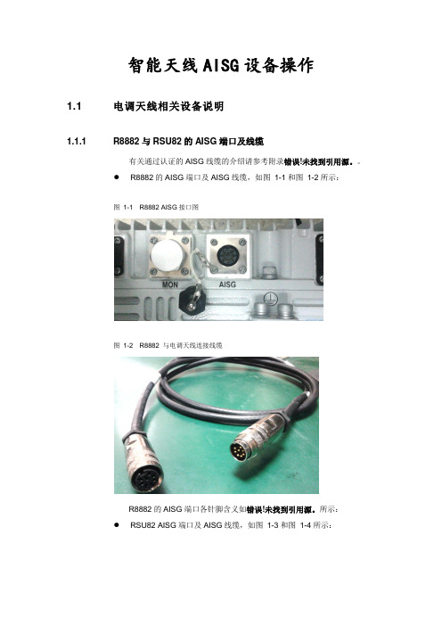
智能天线AISG设备操作1.1 电调天线相关设备说明1.1.1 R8882与RSU82的AISG端口及线缆有关通过认证的AISG线缆的介绍请参考附录错误!未找到引用源。
●R8882的AISG端口及AISG线缆,如图1-1和图1-2所示:图1-1 R8882 AISG接口图图1-2 R8882 与电调天线连接线缆R8882的AISG端口各针脚含义如错误!未找到引用源。
所示:●RSU82 AISG端口及AISG线缆,如图1-3和图1-4所示:图1-3 RSU82 AISG接口图图1-4 RSU82与电调天线连接线缆RSU82的AISG端口各针脚含义如错误!未找到引用源。
所示:1.1.2 电调天线的AISG端口电调天线的AISG端口如错误!未找到引用源。
所示:图1-5 电调天线的AISG端口1.1.3 电调模块RCU的物理实体电调模块RCU用于支持远程电调电子下倾角度,包括电机和AISG接口,RCU如图1-所示;有些天线内置RCU。
安装RCU时需要根据电机的安装说明书进行安装,注意不同品牌电机的安装方法是不同的。
如果安装不正确,校准不会成功。
如果安装时,通过手动调整了天线倾角,通过RET不能查询天线实际的倾角。
所以开局时,一般要校准RET,然后通过OMC/LMT做设置倾角等其它操作。
图1-8 RCU(RET)其中8 Pin Male用于接AISG信号线,8 Pin Female用于RCU级联1.1.4 电调模块RCU的安装连接图1-9 电调模块RCU和AISG的接法2 AISG设备配置AISG设备(电调天线和塔放)的配置流程如图2-1所示:图2-1 AISG设备配置流程图2.1.1 查询天线属性对象1. 在配置管理系统中,选中网元的修改区,然后双击[管理网元→设备→基站附属设备→天线服务功能→天线属性对象],弹出[天线属性对象-列表],如图2-2所示。
图2-2 打开[天线属性对象-列表]2. 在[天线属性对象-列表]中,双击一条天线属性对象记录,就可以查询天线类型的详细信息,如图2-3所示。
DSRF-570平板便携天线操作手册(1)要点

便携式静中通卫星天线系统操作手册目录便携式静中通卫星天线系统操作手册 (1)2.设备外形与接口设置 (2)2.1 设备外观 (2)2.2 设备接口 (5)2.3 显示窗口和操作面板 (6)3.设备开通与收束操作 (7)3.1 静中通天线开通 (7)3.2 静中通天线收束 (10)4.寻星设置界面与操作 (10)4.1 F1界面 (10)4.2 F2界面 (11)4.2.1 F2界面各项意义 (11)4.2.2 F2界面各项数据输入方法 (12)4.3 F3界面 (14)4.4 F4界面 (15)4.5 重新获得GPS定位信息 (15)5、常见问题及解决办法.......................................................................... 错误!未定义书签。
6.系统主要技术指标.............................................................................. 错误!未定义书签。
7. 设备清单............................................................................................... 错误!未定义书签。
1.系统简介本系统型号为DSRF-570,是采用平板卫星天线和DVB-S信号进行自动追踪的静中通卫星通信天线。
系统嵌入了DVB-S卫星信号接收机、GPS接收机和电子倾角传感器,用户只需经简单操作装配两块天线面板,然后启动系统寻星开关,天线便会自动寻找并锁定卫星信号,实现全自动寻星功能。
本系统采用箱式结构,由平板天线(含BUC与LNB)部分与箱式支撑及控制部分组成。
收束状态下,支撑及控制部分收纳于箱内,天线面板收纳于另外的军用布包内,整机可双人搬移。
开通时可经简单操作装配两块天线面板,单键自动按预存卫星参数进行搜星。
第九代Site Master S331L 手持式智能电缆和天线分析仪说明书

技术手册第九代Site Master™S331L手持式智能电缆和天线分析仪具有经典模式和高级模式2 MHz 到 4 GHz 电缆和天线分析仪50 MHz 到 4 GHz 功率计“Site Master 是站点制造商、安装者和维护者和无线服务提供商最值得信赖、最可靠和最值得推荐的电缆和天线分析仪”介绍安立公司非常荣幸的发布其第九代的高性能手持式智能电缆和天线分析仪Site Master™ S331L 。
S331L 全新的设计,是我们综合了我们多年的经验、用户的反馈、现场使用和最新的技术,研发出的最优性价比、专为现场使用、高可靠性、可信赖、结实并易用的智能电缆和天线分析仪。
S331L Site Master 手持电缆和天线分析仪与笔记本连接专为现场应用优化易于使用高效的扫描管理→大于8小时电池工作时间→待机模式和测试模式的快速切换→最高的射频抗干扰能力→内置InstaCal ™自动校准件模块- 快速,一次连接校准→FlexCal ™ 灵活校准模式- 一次校准覆盖所有频率→内置功率计→坚固并可靠→防冲击、灰尘和液体溅落设计→最小、最轻的Site Master ™→集成帮助功能→S331D-类似 经典模式→S331E-类似 高级模式 - 自定义快捷方式 - 增加标记数量 - 全屏显示→多个USB端口→800 x 480 7” TFT 触摸屏 - 大屏幕键盘 - 2个自定义字母数字键盘 - 36个使用字段组合快速命名键→背光键盘→内部存储 >1000 文件 - 存储扫描结果、设置、屏幕截图→快速预览存储的扫描曲线→电缆扫描工具(LST) 软件 - 编辑扫描, 重命名, 归档 - 生成 PDF 或 HTML 报告→标准的*.dat 扫描文件格式→兼容HHST软件 - 被操作人员广泛接受→SweepMasters DIRECT - 提供在线的测试结果传输服务电缆和天线分析仪特点结实,防尘和防滴溅,高可靠性,轻便和小巧Site Master S331L是一款结实、防尘和防水溅、高可靠性、经现场充分验证、并可随时工作的仪表。
CommScope ERA数字分布式天线系统(DAS)用户指南说明书

Deliver L TE and 5Gwhere people areThe need for robust in-building cellular coverage has neverbeen greater. The power to communicate anywhere, anytimethrough our mobile devices is essential—and expected.Dropped calls, spotty coverage and dead zones are nolonger acceptable. Building owners, property managers andenterprises need consistent and reliable mobile service tokeep employees productive, tenants satisfied, and customers connected.CommScope’s all-digital ERA distributed antenna system(DAS) delivers high-performance in-building connectivitywith speed and simplicity. The modular system allows you tosupport today’s cellular coverage and capacity demands andscale to deliver 5G when you’re ready.•Used in venues ranging from under3,000 to 275,000 square meters(30,000 to nearly 3 million square feet)•Allocate capacity among buildings/spaces through a simple drag-and-dropinterfacethan traditional analog DAS gainedthrough fewer and smaller hardwarecomponents•Head-end can be many kilometers/milesaway from covered buildings•Operates on standard IT cablinginfrastructure2 ERA digital distributed antenna system 4G/L TE and 5G connectivity you can count onNow• Work/play in the cloud • Video surveillance • Collaboration/trainingNext• IIoT, real-time control • Remote diagnostics • Remote surgery • Telemedicine• Asset management • Smart wearables• Connected vehicles • Immersive AR/VR • Remote assisted livingFast forward to5G with ERA5G will enable smartphones and other devices to send andreceive large amounts of data at lightning speeds. In additionto faster transmission, 5G offers low latency and definedquality of service to support smart devices like precisioninstruments and autonomous vehicles, for business-criticalapplications.According to the GSMA, even by 2025, 56% of mobileconnections will still use 4G/LTE,* which means thatenterprises will need to support 4G and 5G concurrently.CommScope’s ERA is future-ready to support both. Yourenterprise can migrate with confidence—without ripping andreplacing infrastructure.ERA supports 5G in existing frequency bands with no changesat all. For higher mid-band frequencies such as C-band, ERAoffers a mid-band feeder module and access points; the restof the infrastructure is unchanged. The result is a systemthat supports 2G through 5G over a common set of nodesand cabling.Common platform for commercialcellular and Io TThe internet of things (IoT) can transform the wayenterprises do business and make their facilitiesmore efficient, secure and sustainable. ERA supportscellular IoT standards including LTE Cat M1 andNB-IoT to provide a pervasive and reliable datacoverage layer, without need for a costly dedicatedIoT overlay infrastructure.*Source: GSMA, The Mobile Economy 2020ERA digital distributed antenna system 4G/L TE and 5G connectivity you can count on 3centralized radio access network (C-RAN) hub that digitizes transmissions from base stations• ERA’s head-end features a direct digital interface to compatible third-party baseband unit. This consolidatesthe functionality of up to six remote radio units into asingle card, significantly reducing head-end space, power demand and HVAC costs• Secondary nodes that extend the signal throughout a building or multi-building site• Access points (APs) that convert the digital signal to radio frequency for over-the-air transmission• Compact wideband directional and omnidirectional antennas• Comprehensive monitoring and management software for efficient operation and support, and reduced downtime CommScope’s Advanced Integrated Management and Operating System (AIMOS) helps ensure optimal in-building cellular network performance while simplifying operation and maintenance. The platform has a customizable graphic user interface.AIMOS provides automated support with robust fault, configuration and inventory management capabilities, saving time and money for otherwise manual tasks. It integrates with third-party systems that use SNMP and data interchange formats such as SOAP and XML. AIMOS is available via software license or software as a service (SaaS).Extension NodeSP2SP1SP3site capacityallocationService Provider SiteEdgeERA head-end node and access points4 ERA digital distributed antenna system 4G/L TE and 5G connectivity you can count onERA digital distributed antenna system 4G/L TE and 5G connectivity you can count on 5Public safetyWith growing concern for public safety globally, the need for reliable, ubiquitous, 24/7 cellular network availability is critical. Emergency responder radio coverage is often a requirement in new construction and sometimes even mandated for existing buildings. ERA offers specialized access points that support public safety frequencies, including Band 14 for FirstNet in the U.S. These remotes are available in different transmit power levels to address different building types.CommScope also offers a range of multiband RF repeaters that are designed for public safety applications. These can be used as a signal source to ERA or on their own with direct coaxial connection to multiple antennas.Envision the future with ERACommScope’s all-digital ERA is a next-gen, future-ready solution that minimizes head-end space and powerconsumption and fiber runs, while providing highly flexible mobile capacity allocation. ERA is simpler to install, manage, and operate—all while providing the flexibility to upgrade,expand and grow.6 ERA digital distributed antenna system 4G/L TE and 5G connectivity you can count onFor over 40 years, CommScope has led the industry inhelping companies of all sizes scale, build and sustain robust connections that power more efficient buildings.From office buildings, hospitals, and hotels to airports, stadiums, and collegecampuses, CommScope is a leader in in-building cellular systems. We have in-house expertise and a global network of experienced solution providers.Contact your CommScope solution provider or representative to learn how your network can do more than you ever imagined. Visit to learn more.A trusted partner that delivers it allVisit our website or contact your local CommScope representative for more information.© 2021 CommScope, Inc. All rights reserved.Unless otherwise noted, all trademarks identified by ® or ™ are registered trademarks, respectively, of CommScope, Inc. This document is for planning purposes only and is not intended to modify or supplement any specifications or warranties relating to CommScope products or services. CommScope is committed to the highest standards of business integrity and environmental sustainability with a number of CommScope’s facilities across the globe certified in accordance with international standards, including ISO 9001, TL 9000, and ISO 14001. Further information regarding CommScope’s commitment can be found at https:///About-Us/Corporate-Responsibility-and-Sustainability .BR-112083.2-EN (03/21)CommScope pushes the boundaries of communications technology with game-changing ideas and ground-breaking discoveries that spark profound human achievement. We collaborate with our customers and partners to design, create and build the world’s most advanced networks. It is our passion and commitment to identify the next opportunity and realize a better tomorrow. Discover more at .。
智能天线使用手册

1、引言1.1、智能天线的基本功能〕智能天线定义N 列取向相同的天线按照一定方式排列和激励,利用波的干预原理形成预定波束的阵列结构天线。
〕智能天线基本功能智能天线可以通过改变各天线阵列的激励,其中激励包含幅值和相位,利用波的干预原理形成预定波束。
同时,TD-SCDMA智能天线接入到TD-SCDMA基站后,通过基站的实时自适应信号处理算法,能够自动地产生多个窄波束方向图,实现对移动用户的波束跟踪,并自动地抑制干扰方向的副瓣电平。
从而降低了系统的干扰,提高了系统容量,到达空分多址的目的。
1.2、智能天线与GSM天线的区别〕结构组成区别智能天线由两个或以上天线阵列组成,而GSM系统天线只由一个天线阵列构成。
如图3、4所示:8列单极化智能天线GSM单极化天线图38通道双极化智能天线GSM双极化天线图41.2.2〕功能区别智能天线可以通过改变各天线阵列的激励,利用波的干预原理形成预定波束。
而GSM天线只有一个阵列,其波束在设计时已确定,出厂后不可改变。
2、智能天线的分类2.1、全向天线在360°任意方位上均可进行波束扫描的智能天线阵列。
2.2、定向单极化天线特指采用单极化辐射单元,组成定向阵列,可以在特定方向内进行波束扫描的天线阵列。
2.3、定向双极化天线特指采用双极化辐射单元,组成定向阵列,可以在特定方向内进行波束扫描的天线阵列。
2.4、未来发展前瞻总结一期试验网的经验,业内对智能天线提出了“四化”的要求,即双极化、宽带化、小型化和电调化。
根据目前智能天线行业发展状况,双极化及小型化已经基本实现,并大量应用于二期建网中;宽带化及电调化也在紧锣密鼓的进行中,并且是未来发展的一个重要趋势,除此之外,rru一体化智能天线也是未来发展的一项重要技术。
详细分析如下:2007年初,我国十城市TD-SCDMA试验网络开始建设,当时,智能天线产品只有单极化板状定向智能天线阵和环状全向智能天线阵两种可供选择。
虽然基本上能够满足TD-SCDMA网络实现动态空间滤波对智能天线的电气性能要求,但随着网络建设的深入,在工程实施方面遇到了诸多亟待解决的挑战:1〕天线横截面积大,导致风载荷增加、安全等级下降;2〕天线体积大,公众时有抵触情节,选址难度增加;3〕网络优化需要闭站,且天线下倾角调节难度大;4〕智能天线与城市景观不融洽、不和谐。
AAT自动跟踪天线中文说明书
MyFlyDream Automatic Antenna Tracker使用手册V2.0注意事项感谢您购买MyFlyDream 自动跟踪云台系统(以下简称MFD AAT).请根据本文档熟悉本产品及其操作方法. 本产品是一款精密的机电设备. 请仔细阅读本文档以防止设备受损甚至引致人身伤害.本产品只适用于模型娱乐用途, 请在遵守当地相关法律规定的前提下使用. 因可靠性和精度受多个因素影响: 强烈的电磁干扰, 恶劣的GPS星况或者其他若干原因都可能导致不理想的效果. 使用本产品导致的所有风险和后果由用户承担.我们保留不停改进和提高产品性能的权利, 所以本文档的内容不一定与您手上的产品规格完全符合, 请到我们的网站下载本文档的最新版本:1.系统的组成1.MyFlyDream TrackerB编程器(固件升级用)3.热缩管4.MyFlyDream TeleFlyOSD5.3x8mm不锈钢螺丝及自锁螺母6.MyFlyDream AATDriver2.工作原理MFD AAT设计目的是为FPV系统提供全方位的信号接收能力.FPV飞行中,我们为了获得更好的视频信号接收质量, 希望采用高增益的接收天线. 但高增益的天线往往伴随着狭窄的有效角度. MFD AAT的设计就是为了解决FPV飞行时定向天线难以保持在最佳收发角度的问题.为了组成完整的系统,用户需要在飞机上安装TeleFlyOSD模块. TeleFlyOSD从飞机上的GPS 读取数据, 把飞机的坐标和高度信息进行编码调制, 通过无线的音频通道(通常会使用无线图传的伴音通道)发射回来.地面部分把接收到的音频信号后传给AATDriver. AATDriver对信号进行解调和解码,取得飞机的位置信息. 和初始坐标比较后, 得到飞机目前相对云台的方位角和距离,高度等信息. AATDriver把这些信息发送给云台. 云台驱动内部的舵机,使定向天线对准飞机所在的位置.3.性能参数MFD AAT系统内部有高质量的电器滑环,可以连续无限旋转而不产生线缆缠绕的问题.内建的电子罗盘使得系统可以即插即用, 无需额外的方向初始化操作.AATDriver:4.连接与调试1). TeleFlyOSD的安装TeleFlyOSD各部分简介引线颜色和功能*极限输出电流: 13V供电时<80ma, 8V供电时<120ma. 请注意所使用的GPS耗电量勿超出范围.连接TeleFlyOSDTeleFlyOSD既可以使用一个独立的GPS, 亦可与其他OSD共用一个GPS.使用独立的GPS请参考接线图A。
智能天线参数权值的说明文档及设置建议 (1)
华为技术分册 V1.3
2009 年 7 月
前言
因为 TD 系统的智能天线特性,如果天线类型和权值没有正确 配置,将出现由于配置错误而导致系统覆盖变形、网络性能变差、 出现越区覆盖和弱覆盖、TS0 干扰等问题,严重影响网络性能,通 过 OMC-R 对 TD 系统智能天线权值进行呈现和修改,不但可以避 免这些问题,还可以实现灵活地调整小区覆盖形状,根据实际需求 控制天线波束宽度等功能,尤其适用于特殊场景的优化。
-1-
TD-SCDMA 智能天线系统权值配置手册 华为技术分册
1.2 基本流程....................................................................................................12 1.3 基本概念....................................................................................................12 1.3.1 CellBeam 实例 .........................................................................................12 1.3.2 CellBeam 实例的脚本 .............................................................................12 1.3.3 基本命令.................................................................................................13 1.3.4 天线权值索引.........................................................................................13 1.3.5 天线权值属性 .........................................................................................13 第二章 配置基本原则.........................................................................................15 第三章 准备权值数据.........................................................................................15 3.1 手工计算方法............................................................................................15 3.2 利用工具将幅度相位原始数据自动转换为 16 进制数据.........................16 3.3 利用工具将 16 进制数据自动转换为幅度相位值 ....................................17 第四章 维护权值库.............................................................................................17 4.1 通过 LMT-B 或 OMC-B 向权值库追加单7 4.2 通过 LMT-B 和脚本向权值库批量追加新的天线权值 ............................18
NANO mXTEND 迷你高效蓝牙 Wi-Fi天线说明书

NANO mXTEND TM: MINIATURE AND HIGH EFFICIENCY BLUETOOTH/WI-FI ANTENNAUSER MANUALNANO mXTEND TM (NN02-101)NANO mXTEND TMMINIATURE AND HIGH-EFFICIENCY BLUETOOTH/WI-FIANTENNANN02-101NANO mXTEND TM | Bluetooth & Wi-Fi Operating range: 2400 – 10600 MHzBest for: 2400 – 2500 MHzDimensions : 3.0 mm x 2.0 mm x 0.8 mmWhat is the NANO mXTEND TM?The NANO mXTEND TM is the smallest Virtual Antenna® chip to date. Featuring a size of only 3 mm x 2 mm x 0.8 mm, this off-the-shelf chip antenna has been designed to fit almost every IoT device from entry-level to high-end products. The NANO mXTEND TM is enabled by Virtual Antenna® technology, thus featuring the unique properties of this class of products: easy to use; versatile, and broadly tunable. The NANO mXTEND TM is available for Bluetooth, Wi-Fi, Wi-SUN, and any wireless connectivity protocol operating in the 2.4 - 2.5 GHz band. Due to Ignion’s proprietary Virtual Antenna® technology, this chip antenna is non-resonant and therefore broadly tunable, enabling additional frequency bands to be supported by the same antenna part and released in the future.As with every other Virtual Antenna® chip, the NANO mXTEND TM is available through Ignion’s Antenna Intelligence Cloud tool, enabling predictable design and performance throughout the entire product development cycle. Moreover, the NANO mXTEND TM is built on a glass epoxy substrate, making its manufacturing broadly available and therefore resilient against shortage.Material: The NANO mXTEND TM antenna booster is built on a glass epoxy substrate.What is the NANO mXTEND TM used for?The NANO mXTEND TM is suitable for embedding an antenna into any wireless device requiring optimum performance in a small, cost-effective package for operating in the Bluetooth/Wi-Fi/Wi-SUN ISM 2.4 GHz frequency bands, including:▪Asset Trackers▪Smart Tags▪Earphones and Headsets ▪Wearables▪Logistic Trackers▪Health sensors ▪Animal Trackers▪Security Sensors▪Service Buttons▪Environmental Sensors ▪IoT Developer Kits▪Wireless Sniffing SensorsWhat differentiates the NANO mXTEND TM from other chip antennas?Like every other Virtual Antenna® product, the NANO mXTEND TM is frequency neutral, meaning that its frequency response is not determined by the antenna component but designed by the electronics engineer. Virtual Antenna® technology provides the broadest range of connectivity options with desired antenna performance in the smallest ever form factor. This unique technology enables the whole mXTEND TM range of components to become tiny, off-the-shelf, surface-mount (SMD) electronic chips while still providing connectivity with multiple frequency bands and meeting the requirements of most wireless devices’ architectures and form factors. Being non-resonant, the whole antenna performance can be customized through a shorter and easier design cycle by means of a matching circuit, while benefiting at the same time from a robust, reliable, and cost-effective manufacturing process because of the chip, SMD form factor. Also, the NANO mXTEND TM‘s architecture is not using ceramic materials to achieve miniaturization, which ensures a pervasive availability of raw materials thus making the supplychain resilient to shortage and price fluctuations.HOW TO EMBED A VIRTUAL ANTENNA®MECHANICAL SPECIFICATIONSASSEMBLY AND MANUFACTURINGPACKAGINGThe NANO mXTEND TM for Bluetooth/Wi-Fi 9 CORNER MOUNTING CONFIGURATION 9 MATCHING NETWORK 11 VSWR AND TOTAL EFFICIENCY 12 RADIATION PATTERNS, GAIN, AND EFFICIENCY 13 EDGE MOUNTING CONFIGURATION 14 MATCHING NETWORK 15 VSWR AND TOTAL EFFICIENCY 16 RADIATION PATTERNS, GAIN, AND EFFICIENCY 17 MECHANICAL SPECIFICATIONS 18 DIMENSIONS, TOLERANCES, AND RoHS 18 INK COLOR RANGE 18 RECOMMENDED FOOTPRINT FOR THE NN02-101 19 ASSEMBLY AND MANUFACTURING 21PACKAGING 23How to embed Virtual Antenna ®Design with Virtual Antenna ® in 1-2-3https://ignion.io/design-center/tutorials-webinars/STEP 2: Design your matching network1. Through a combination of inductors & capacitorsobtain 50 Ohms of antenna impedance to optimize the transfer of energy to your antenna2. It is critical to fine-tune your MN throughout theentirety the design process to achieve your desired frequency responseLook here for an example of a matching network for a Virtual Antenna ® product application via simulation Scan this QR code to see our videos highlighting these three easy stepsNeed further help? Easy start with Antenna Intelligence CloudDo you need more help with your antenna for your device?Use our Antenna Intelligence Cloud service and get your ready-to-test, proof-of-concept antenna design especially simulated for your platform free of charge 1, and in 24 hours .https://www.ignion.io/antenna-intelligence/1 Subject to terms and conditions here .Scan QR code to be taken to our AntennaIntelligence Cloud pageThe NANO mXTEND™ has been designed for Bluetooth/Wi-Fi connectivity at 2.4 GHz. An optimum tuning of this chip at the 2.4 GHz band is achieved through a matching network. Due to its versatility, the chip antenna component can be mounted both on the corner or on the center of an edge of the printed circuit board (PCB) of your wireless device just by changing the matching network. The table below includes a quick reference guide for the antenna specifications on a reference design of 80 x 40 mm, as well as the set-up matching network and performance for both a corner and an edge mounting configuration.QUICK REFERENCE GUIDETechnical Specs for the NANO mXTEND™ in the corner configuration: Technical features 2400 – 2500 MHzAverage Efficiency >55 %Peak Gain 2.4 dBiVSWR < 2.5:1Radiation Pattern OmnidirectionalPolarization LinearWeight (approx.) 0.01 g.Temperature -40 to +125 ºCImpedance 50 ΩDimensions3.0 mm x 2.0 mm x 0.8 mm(L x W x H)Table 1 – Technical Features. Measurements from the evaluation board (Figure 1) Technical Specs for the NANO mXTEND™ in the edge configuration: Technical features 2400 – 2500 MHzAverage Efficiency >65 %Peak Gain 2.4 dBiVSWR < 3.0:1Radiation Pattern OmnidirectionalPolarization LinearWeight (approx.) 0.01 g.Temperature -40 to +125 ºCImpedance 50 ΩDimensions3.0 mm x 2.0 mm x 0.8 mm(L x W x H)Table 2– Technical Features. Measurements from the evaluation board (Figure 4)CORNER MOUNTING CONFIGURATIONThe NANO mXTEND TM is ready and recommended for corner mounting in those devices where this region is available for antenna placement. This section details a corner mounting design on a reference ground plane of 80 mm x 40 mm including a clearance area of 5 mm x 5 mm (Figure 1). Other ground plane sizes and clearances can be implemented by adapting the matching network.MeasuremmA 80B 75C 40D 5E 5 F3Tolerance : ±0.2 mmD: Length of clearance area.Figure 1 - EB_NN02-101_c_BT. Evaluation board configured to provide operation at Bluetooth (2400 – 2500MHz).This product and its use are protected by at least one or more of the following patents and patent applications PAT. US 62/529032; and other domestic and international patents pending.MATCHING NETWORKThe NANO mXTEND TM antenna booster needs a matching network to ensure optimal performance in the 2.4 GHz – 2.5 GHz frequency range. This section presents a suitable matching network for the corner mounting configuration (Figure 7). Please note that different form factors, RF ground planes, and nearby components may require a different matching network.If you need assistance to design your matching network beyond this application note, please contact *****************, or if you are designing a different device size or a different frequency band, we can assist you in less than 24 hours. Please, try our free-of-charge1 Antenna Intelligence Cloud, which will get you a complete design report including a custom matching network for your device in 24h1. Additional information related to Ignion’s range of R&D services is available at: https://ignion.io/rdservices/2.4 GHz – 2.5 GHz8.7 nH LQW18AN8N7G808.2 nH LQW18AN8N2C805.8 nH LQW15AN5N8B80Figure 2 –Matching network implemented on the Evaluation Board (Figure 1) for covering Bluetooth from 2.4GHz to 2.5GHz.For an optimal result, the use of high-quality factor (Q) and tight tolerance components is highly recommended (e.g., Murata components with part numbers as shown in Figure 2). The antenna performance is always conditioned by its operating environment meaning that differences in the device, including differences in printed circuit board sizes, components near the antenna, displays, batteries, covers, connectors, etc. affect the antenna performance. Accordingly, placing pads compatible with 0402 and 0603 SMD components for a matching network as close as possible to the feeding point of the antenna element is highly recommendable. It is also recommendable to do this in the ground plane area, not in the clearance area. By tuning the matching network in your final design after your final surrounding components are in place (batteries, displays, covers, etc.) you will be able to optimize the antenna performance without changing the antenna part or the design.1 See terms and conditions for a free Antenna Intelligence Cloud service in 24h at:https://www.ignion.io/antenna-intelligence/VSWR (Voltage Standing Wave Ratio) and Total Efficiency versus Frequency (GHz).Figure 3 - VSWR and Total Efficiency for the 2.4 – 2.5 GHz frequency range as observed on the evaluation board EB_NN02-101_c_BT (Figure 1).2.4 – 2.5GHzNANO mXTEND™ ɳa 2400MHzɳa 2500MHz Min Max Av. ɳaOn the corner 54.9 57.1 54.9 63.2 60.1 Table 3 - Antenna efficiency comparison considering the evaluation board EB_NN02-101_c_BT (Figure 1).The NANO mXTEND TM operates at the required Bluetooth/Wi-Fi frequency spectrum with high-efficiency values. Please note that its high performance can be sustained even with a reducedclearance area.RADIATION PATTERNS, GAIN, AND EFFICIENCYMeasurement System Set-UpEvaluation Board in Plane XYθ = 90º Plane XY at 2450 MHzφ= 0º Plane XZ at 2450 MHzφ= 90º Plane YZ at 2450 MHz GainPeak Gain 2.4 dBiAverage Gain across the band 2.2 dBiGain Range across the band (min, max) 1.9 dBi <–> 2.4 dBi EfficiencyPeak Efficiency 75.4 %Average Efficiency across the band 71.9 %Efficiency Range across the band (min, max) 66.3 – 75.4 %Table 4 – Antenna Gain and total efficiency from the evaluation board (Figure 1) Bluetooth band. Measurements made in the STARLAB 18 anechoic chamber.EDGE MOUNTING CONFIGURATIONIn devices such as dual-hand gaming handhelds and landscape handheld devices, the center of the edge can be the ideal placement area for your chip antenna, This section details a design example and evaluation board (80 mm x 40 mm with 4 mm x 4 mm of ground clearance) in such an edge mounting configuration (Figure 4).MeasuremmA 80B 40 C5Tolerance : ±0.2 mmC: Length of clearance area.Figure 4 - EB_NN02-101_m_BT. Evaluation board providing operation at Bluetooth (2400 – 2500 MHz).MATCHING NETWORKBy simply changing the matching network, the NANO mXTEND TM can also deliver optimal performance in an edge mounting configuration. A suitable matching network for edge mounting in the reference board pictured above is shown in Fig.5. Please note that different form factors of your wireless device and its RF ground planes, and the proximity of other elements such as shields, covers, connectors and the like might result in the need for a fine-tuning of the matching network.If you need assistance to design your matching network beyond this application note, please contact *****************, or if you are designing a different device size or a different frequency band, we can assist you in less than 24 hours. Please, try our free-of-charge1 Antenna Intelligence Cloud, which will get you a complete design report including a custom matching network for your device in 24h2. Additional information related to Ignion’s range of R&D services is available at: https://ignion.io/rdservices/2.4 GHz – 2.5 GHz--0.4pF GJM1555C1HR40WB010.3pF GJM1555C1HR30WB010.3pF GJM1555C1HR30WB01Figure 5 –Matching network implemented in the Evaluation Board (Figure 4) for covering Bluetooth from 2.4GHz to 2.5GHz.To ensure optimal results, the use of high-quality factor (Q) and tight tolerance components is highly recommended (e.g. Murata components with part numbers as shown in Figure 5). The antenna performance is always conditioned by its operating environment meaning that differences in the device, including differences in printed circuit board sizes, components near the antenna, displays, batteries, covers, connectors, etc. affect the antenna performance. Accordingly, placing pads compatible with 0402 and 0603 SMD components for a matching network as close as possible to the feeding point of the antenna element is highly recommendable. It is recommended to do this in the ground plane area, not in the clearance area. By tuning the matching network in your final design after your final surrounding components are in place (batteries, displays, covers, etc.) you will be able to optimize the antenna performance without changing the antenna part, or the design.2 See terms and conditions for a free Antenna Intelligence Cloud service in 24h at:https://www.ignion.io/antenna-intelligence/VSWR (Voltage Standing Wave Ratio) and Total Efficiency versus Frequency (GHz).Figure 6 - VSWR and Total Efficiency for the 2.4 – 2.5 GHz frequency range configured to provide operation the evaluation board EB_NN02-101_m_BT (Figure 4).2400 – 2500 MHzNANO mXTEND™ ɳa 2400MHzɳa 2500MHz Min Max Av. ɳaOn the middle 60.1 63.6 60.1 77.3 71.7 Table 5 - Antenna efficiency comparison configured to provide operation the evaluation board EB_NN02-101_m_BT (Figure 4).The NANO mXTEND TM operates at the required Bluetooth/Wi-Fi frequency spectrum with high efficiency values. Please note that its high performance can be sustained even with the small5x5 mm clearance area.RADIATION PATTERNS, GAIN, AND EFFICIENCYMeasurement System Set-UpEvaluation Board in Plane XYθ = 90º Plane XY at 2450 MHzφ = 0º Plane XZ at 2450 MHzφ = 90º Plane YZ at 2450 MHzGainPeak Gain1.1 dBi Average Gain across the band0.85 dBi Gain Range across the band (min, max) 0.3 dBi <–> 1.1 dBiEfficiencyPeak Efficiency73.7 % Average Efficiency across the band69.6 % Efficiency Range across the band (min, max)70.0 – 73.7 %Table 6 – Antenna Gain and total efficiency from the evaluation board (Figure 4) Bluetooth band. Measurements made in the STARLAB 18 anechoic chamber.MECHANICAL SPECIFICATIONSDIMENSIONS, TOLERANCES, AND RoHSTOPSIDEBOTTOMDimensionmm DimensionmmA2.0 B3.0 C 0.25 D 1.0 E 0.5 F 1.3 G 0.6 H 0.8 I0.35J0.8Figure 7 - NANO mXTEND TM antenna booster dimensions and tolerances.The NANO mXTEND TM (NN02-101) antenna booster is compliant with the restriction of the use of hazardous substances (RoHS ). For more information, please contact **************.INK COLOR RANGEThe next figure shows the range of colors in the NANO mXTEND TM antenna booster:Acceptable color rangeRECOMMENDED FOOTPRINT FOR THE NN02-101See below the recommended footprint dimensions for the NANO mXTEND TM (NN02-101) antenna booster on the corner .MeasuremmA 1.0B 0.5C 1.3D 0.8 E0.15Tolerance : ±0.05mmFigure 8 - Footprint dimensions for the NANO mXTEND™ (NN02-101) antenna booster (on the corner).See below the recommended footprint dimensions for the NANO mXTEND T M (NN02-101) antenna booster in the middle .Tolerance : ±0.05mmMeasuremmA 1.875B 1.35C 0.5D 1.0E 3.15 F4.0Figure 9 - Footprint dimensions for the NANO mXTEND™ (NN02-101) antenna booster (on the middle).For additional support in the integration process, please contact *****************.ASSEMBLY AND MANUFACTURINGFigure 10 shows the back and front views of the NANO mXTEND TM(NN02-101) antennabooster.Figure 10 – Pads of the NANO mXTEND TM (NN02-101)antenna booster.As a surface mount device (SMD), the NANO mXTEND TM antenna booster is compatible withindustry standard soldering processes. The basic assembly procedure for the NANOmXTEND TM antenna booster is as follows:1. Apply a solder paste on the pads of the PCB. Place the NANO mXTEND TM antenna boosteron the board.2. Perform a reflow process according to the temperature profile detailed in Figure 11.3. After soldering the NANO mXTEND TM antenna booster to the circuit board, perform acleaning process to remove any residual flux. Ignion recommends conducting a visualinspection after the cleaning process to verify that all reflux has been removed.The figure below shows the soldering details obtained after a correct assembly process:Figure 11 - Soldering detailsNOTE (*): Solder paste thickness after the assembly process will depend on the thickness of the soldering stencil mask. A stencil thickness equal to or larger than 127 microns (5 mils) isrequired.The NANO mXTEND TM (NN02-101) antenna booster can be assembled following the Pb-free assembly process. According to the IPC/JEDEC J-STD-020C Standard, the suggested temperature profile is as follows:Phase Profile featuresPb-Free assembly (Sn Ag Cu) RAMP-UPAvg. Ramp-up Rate (Tsmax to Tp) 3 ºC / second (max.) PREHEAT- Temperature Min (Tsmin)- Temperature Max (Tsmax) - Time (tsmin to tsmax)150 ºC 200 ºC60-180 seconds REFLOW- Temperature (TL) - Total Time above TL (tL) 217 ºC60-150 seconds PEAK - Temperature (Tp) - Time (tp) 260 ºC 20-40 seconds RAMP-DOWNRate6 ºC/second max Time from 25 ºC to Peak Temperature8 minutes maxTable 7 – Recommended soldering temperatures.The next graphic shows the temperature profile (grey zone) for the NANO mXTEND TM antenna booster assembly process reflow ovens.Figure 12 – Temperature profilePACKAGINGThe NANO mXTEND TM (NN02-101) antenna booster is delivered in tape and reel packaging.Measure mm A0 3.6 ± 0.1 B0 7.5 ± 0.1 K0 2.5 ± 0.1 W 16.0 ± 0.3 P 8.0 ± 0.1 T 0.3 ± 0.05Figure 13 -Tape dimensions and tolerances.Reel Capacity : 2500 pcsMeasure Mm A 330 ± 1.0 G 16.4 ± 0.1 t max20.4 ± 0.1Figure 14 - Reel dimensions and capacity.Ignion products and solutions are protected by Ignion patents .All information contained within this document is property of Ignion and is subject to change without prior notice. Information is provided “as is” and without warranties. The copy or reproduction of this information without prior approval is prohibited.Ignion is an ISO 9001:2015 certified company. All our antennas are lead-free and RoHS compliant.ISO 9001: 2015 CertifiedContact:***************** +34 935 660 710BarcelonaAv. Alcalde Barnils, 64-68 Modul C, 3a pl. Sant Cugat del Vallés08174 BarcelonaSpainShenzhenTopway Information Building,2303 Room No.3369, Binhai Avenue, Nanshan District Shenzhen, Guangdong 518000China+86138****8470Tampa8875 Hidden River ParkwaySuite 300Tampa, FL 33637USA。
- 1、下载文档前请自行甄别文档内容的完整性,平台不提供额外的编辑、内容补充、找答案等附加服务。
- 2、"仅部分预览"的文档,不可在线预览部分如存在完整性等问题,可反馈申请退款(可完整预览的文档不适用该条件!)。
- 3、如文档侵犯您的权益,请联系客服反馈,我们会尽快为您处理(人工客服工作时间:9:00-18:30)。
1、引言1.1、智能天线的基本功能1.1.1)智能天线定义N 列取向相同的天线按照一定方式排列和激励,利用波的干涉原理形成预定波束的阵列结构天线。
1.1.2)智能天线基本功能智能天线可以通过改变各天线阵列的激励,其中激励包含幅值和相位,利用波的干涉原理形成预定波束。
同时,TD-SCDMA智能天线接入到TD-SCDMA基站后,通过基站的实时自适应信号处理算法,能够自动地产生多个窄波束方向图,实现对移动用户的波束跟踪,并自动地抑制干扰方向的副瓣电平。
从而降低了系统的干扰,提高了系统容量,达到空分多址的目的。
1.2、智能天线与GSM天线的区别1.2.1)结构组成区别智能天线由两个或以上天线阵列组成,而GSM系统天线只由一个天线阵列构成。
如图3、4所示:8列单极化智能天线 GSM单极化天线图38通道双极化智能天线 GSM双极化天线图41.2.2)功能区别智能天线可以通过改变各天线阵列的激励,利用波的干涉原理形成预定波束。
而GSM天线只有一个阵列,其波束在设计时已确定,出厂后不可改变。
2、智能天线的分类2.1、全向天线在360°任意方位上均可进行波束扫描的智能天线阵列。
2.2、定向单极化天线特指采用单极化辐射单元,组成定向阵列,可以在特定方向内进行波束扫描的天线阵列。
2.3、定向双极化天线特指采用双极化辐射单元,组成定向阵列,可以在特定方向内进行波束扫描的天线阵列。
2.4、未来发展前瞻总结一期试验网的经验,业内对智能天线提出了“四化”的要求,即双极化、宽带化、小型化和电调化。
根据目前智能天线行业发展状况,双极化及小型化已经基本实现,并大量应用于二期建网中;宽带化及电调化也在紧锣密鼓的进行中,并且是未来发展的一个重要趋势,除此之外,rru一体化智能天线也是未来发展的一项重要技术。
详细分析如下:2007年初,我国十城市TD-SCDMA试验网络开始建设,当时,智能天线产品只有单极化板状定向智能天线阵和环状全向智能天线阵两种可供选择。
虽然基本上能够满足TD-SCDMA网络实现动态空间滤波对智能天线的电气性能要求,但随着网络建设的深入,在工程实施方面遇到了诸多亟待解决的挑战:1)天线横截面积大,导致风载荷增加、安全等级下降;2)天线体积大,公众时有抵触情节,选址难度增加;3)网络优化需要闭站,且天线下倾角调节难度大;4)智能天线与城市景观不融洽、不和谐。
5)天线与rru之间接线复杂,工程量大,线损大,难于隐蔽等缺点。
应对第1、2点挑战,要求发展小型化智能天线,实现小型化的最佳途径是,采用4列双极化阵列,通过引入极化分集增益来弥补因天线口径减少而引起的天线增益下降。
实验室测试和网络规模试用都表明,小型化的双极化智能天线,其宽度减小了一半,但网络性能与常规8列天线水平相当,已经成为第二期TD-SCDMA网络建设的主力产品之一。
应对第3、4点挑战,要求发展双极化的电调智能天线。
首先TD-SCDMA 网络同CDMA网络、WCDMA网络一样,也存在呼吸效应。
CDMA和WCDMA网络的实践表明,在解决呼吸效应方面,采用电调天线对覆盖蜂窝实施动态调整是最有效的方法,国外的WCDMA网络电调天线的使用量均超过了75%。
其次,政府和公众都预期对3G网络覆盖功率密度能够和用户数量及数据流量实现动态匹配,从而达到节能环保及减少电磁辐射污染的目的。
第三,TD-SCDMA网络的动态空间滤波和功率调配优势,在通信容量极高的城区可以得到淋漓尽致的发挥,但城区布网的特点是蜂窝较密,需要大量采用大倾角波束指向,而过大的机械下倾角会带来严重的波束畸变,造成同频干扰。
第四,许多站址需要美化、隐蔽及环境和谐,如果按照惯性思维采用机械调整下倾角度,则天线整体将占据更大的空间体积,这给隐蔽工作带来更大的困难,无法让公众接受。
综上所述,在未来TD-SCDMA网工程建设和优化中,电调智能天线不可避免的登上舞台,成为智能天线技术进一步发展的主旋律。
目前TD-SCDMA网络使用的是2010~2025MHz频段,只有15MHz带宽。
对于拥有13亿人口的中国,这远远不够,未来必将启用第二、第三频段,目前规划的是1880~1920MHz,2300~2400MHz。
如果天线能够同时满足这三个频段,或者其中两个频段,在未来扩充频段时,就不需要补充天线了。
因此,发展宽频带天线,具有重要的经济意义。
应对第5点挑战,要求发展一体化的智能天线。
一体化智能天线将rru与智能天线采用盲插式接头结合在一起,天线与RRU无需电缆连接,外形美观,施工便利;减少系统电缆连接,提高系统可靠性;减小射频损耗,提高系统性能;方便安装、拆装,安装时间降低90%,便于施工与维护。
因此,发展一体化智能天线是非常具有实用意义的。
所以,综合以上分析表明,智能天线的未来发展趋势将是“宽带化、电调化和一体化”。
3、相关基本概念3.1、单元波束、广播波束、业务波束单元波束定义为:智能天线单一阵列的接收或者发射的水平面辐射方向图。
广播波束定义为:对智能天线阵列施加特定的幅度和相位激励所形成的全向覆盖或扇区覆盖的辐射方向图。
业务波束定义为:对智能天线阵列施加特定的幅度和相位激励所形成的在工作角域内具有任意波束指向扫描以及具有高增益窄波束的方向图。
3.2、波束宽度波束宽度指波束的主瓣中功率电平下降一半(3dB)的角度范围。
3.3、波束权值a)什么是权值,什么是TD广播波束权值;➢权值是天线各端口所施加的特定激励信号的量化表示方法,天线端口施加特定激励的目的是为了得到具有特定覆盖效果的方向图。
➢TD广播权值是为得到满足特定小区广播信道覆盖的方向图而对各天线端口施加的激励信号,权值可以表示为幅度/相位方式,幅度一般用电压值表示,单位为伏特,(也可以用功率表示,单位:瓦),相位用角度作单位。
b)不同厂家天线广播波束权值不同;➢各厂家的单元列方向图因天线内部具体实现结构的不同而存在差异,因为广播波束是在权值作用下各单元列方向图的矢量叠加,单元方向图不同,自然可能存在权值差异;➢即便对于完全相同的单元方向图,因广播波束的要求存在一定范围(比如半功角65±5,60度下降10~15dB),所对应的权值自然也不是唯一的。
c)不同类型天线广播波束权值不同,特别是单极化双极化完全不同,简述单极化天线和双极化天线权值的特点;主要差别是权值数目不同,单极化天线需要8列天线同时工作,对应的权值有16个数值(包括8个幅度和8个相位);双极化天线只需要4列天线同时工作,对应的权值有8个数值(包括4个幅度和4个相位)。
d)给予同一面天线不同的广播波束权值激励,可以得到不同宽度的广播波束,从而达到用软件调整广播波束宽度的目的;智能天线基本应用原理就是通过不同权值得到不同的波束(包括业务波束,广播波束),广播波束可以由特定权值实现,不同的权值可以得到不同宽度的广播波束,是智能天线的应用优势,可以不改变硬件,完全使用软件方法实现波束的动态调整。
e)对于同一面天线可能存在若干组不同的广播波束权值,都能够实现对特定宽度(如65度)的广播波束进行赋形,这些组权值可能都是正确的,但只有一组是最优的。
前面提到,不同的天线结构将有不同的单元方向图,权值的作用是对特定的单元方向图进行加权得到满足应用需要的阵列方向图,我们认为绝对最优的解是不能得到的,可以从两方面理解:(1)“只有更好,没有最好”,“最好”的东西可以被“更好”的超越,权值的获得是不断优化的过程;(2)存在相对最优权值,但有其存在的前提,(a)针对明确的天线结构,即针对具体的单元列方向图;(b)确定最优的判断标准,是3dB内起伏小,3dB宽度稳定,60度下降稳定或EIRP损耗小等等判断方法,缺乏判断标准的最优是没有意义的,而满足所有标准的权值难于获得,即便暂时获得,也不能断定没有更好的出现。
4、广播波束权值与广播波束赋形的关系4.1、不同类型智能天线65°广播波束权值与对应方向图4.1.1、定向单极化天线65°广播波束权值与对应方向图4.1.2、定向双极化天线65°广播波束权值与对应方向图极化类型 广播波束宽度权值 端口1 端口2 端口3 端口4 端口5 端口6 端口7 端口8 双极化65 度幅度∣Ii ∣0.53 1 1 0.53 0.53 1 1 0.53 相位-100-100-100-100方向图4.2、同一面智能天线加以不同权值激励得到的不同宽度广播波束赋形举例极化类型 广播波束宽度 权值 端口1 端口2 端口3 端口4 端口5 端口6 端口7 端口8 单极化65 度幅度∣Ii ∣0.50 1.0 1.0 0.71 0.71 1.0 1.0 0.50 相位128.0-143.0-62.0-31.0-31.0-62.0-143.0128.0方向图(以双极化天线为例)4.2.1、30°广播波束的权值与方向图极化类型广播波束宽度权值端口1端口2端口3端口4端口5端口6端口7端口8双极化30 度幅度∣Ii∣0.53110.530.53110.53相位-4500-45-4500-45方向图4.2.2、65°广播波束的权值与方向图极化类型广播波束宽度权值端口1端口2端口3端口4端口5端口6端口7端口8双极化65 度幅度∣Ii∣0.53110.530.53110.53相位-10000-100-10000-100方向图4.2.3、90°广播波束的权值与方向图4.2.4、其他宽度广播波束举例极化类广播波束权值端端口端口3 端口4端口5 端口6 端口7 端口8极化类型 广播波束宽度权值 端口1 端口2 端口3 端口4 端口5 端口6 端口7 端口8 双极化90 度幅度∣Ii ∣ 0.53 1 1 0.53 0.53 1 1 0.53 相位-120-120-120-120方向图精品可编辑双极化 45 度 幅度∣Ii ∣0.45 1 1 0.45 0.45 1 1 0.45 相位-85-85-85-85方向图4.3、错误的广播波束权值应用举例单极化误用双极化系数双极化误用单极化系数。