X242-883B中文资料
飞利浦 B Line 222B9 242B9 显示器用户手册说明书

/welcome241B8B Line222B9/242B9ZH 用户手册 1 客户服务与保修 16故障排除和常见问题解答20目录1. 重要 (1)1.1 安全措施与维修 (1)1.2 标志说明 (2)1.3 产品和包装材料的废弃 (3)2. 设置显示器 (4)2.1 安装 (4)2.2 操作显示器 (5)3. 图像优化 (8)3.1 SmartImage (8)3.2 SmartContrast (9)4. SmoothT ouch (10)5. 技术规格 (11)5.1 分辨率和预设模式 (14)6. 电源管理 (15)7. 客户服务与保修 (16)7.1 Philips平板显示器像素缺陷规定167.2 客户服务与保修 (19)8. 故障排除和常见问题解答 (20)8.1 故障检修 (20)8.2 一般常见问题解答 (21)8.3 SmoothT ouch (23)1. 重要此电子版用户指南适合使用Philips显示器的所有用户。
请在使用您的显示器之前花点时间阅读本用户手册。
它包含与使用显示器相关的重要信息和注意事项。
产品享受Philips保修须符合下列条件:产品适当用于其设计目的、符合操作说明、返修时提供原始帐单或付款收据,帐单或收据应载明购货日期、销售商名称、产品型号及生产号。
1.1 安全措施与维修警告使用本文档中未介绍的控制、调整或过程可能导致碰撞、电气危险和/或机械危险。
连接和使用电脑显示器时,请阅读并遵循以下说明。
操作• 请使显示器远离阳光直接照射、明亮强光线、以及任何其他热源。
长期暴露于此类环境可能导致显示器褪色和损坏。
• 移开任何可能掉入通风孔的物品或者会妨碍显示器电子器件正常冷却的物品。
• 请勿堵塞机壳上的通风孔。
• 放置显示器时,确保电源插头和插座便于插拔。
• 如果通过拔掉电源线或直流电源线关闭显示器电源,则在重新连接电源线或直流电源线以进行正常操作之前,必须等待6秒钟。
• 请务必使用由Philips提供的经过认可的电源线。
WBH-822A技术及使用说明书V1.0

封装形式说明

封装形式说明图片1电子元器件,又叫电子芯片,半导体集成电路,广泛应用于各种电子电器设备上.封装形式:封装形式是指安装半导体集成电路芯片用的外壳.它不仅起着安装,固定,密封,保护芯片及增强电热性能等方面的作用,而且还通过芯片上的接点用导线连接到封装外壳的引脚上,这些引脚又通过印刷电路板上的导线与其他器件相连接.衡量一个芯片封装技术先进与否的重要指标是芯片面积与封装面积之比,这个比值越接近1越好.封装大致经过了如下发展进程:结构方面:TO->DIP->LCC->QFP->BGA ->CSP;材料方面:金属,陶瓷->陶瓷,塑料->塑料;引脚形状:长引线直插->短引线或无引线贴装->球状凸点;装配方式:通孔插装->表面组装->直接安装.英文简称/英文全称/中文解释/图片(1)DIPDouble In-line Package双列直插式封装.插装型封装之一,引脚从封装两侧引出,封装材料有塑料和陶瓷两种.DIP是最普及的插装型封装,应用范围包括标准逻辑IC,存贮器LSI,微机电路等.(2)PLCCPlastic Leaded Chip CarrierPLCC封装方式,外形呈正方形,32脚封装,四周都有管脚,外形尺寸比DIP封装小得多.PLCC封装适合用SMT表面安装技术在PCB上安装布线,具有外形尺寸小,可靠性高的优点.(3)PQFPPlastic Quad Flat PackagePQFP封装的芯片引脚之间距离很小,管脚很细,一般大规模或超大规模集成电路采用这种封装形式,其引脚数一般都在100以上.(4)SOPSmall Outline Package1968~1969年菲为浦公司就开发出小外形封装(SOP).以后逐渐派生出SOJ(J型引脚小外形封装),TSOP(薄小外形封装),VSOP(甚小外形封装),SSOP(缩小型SOP),TSSOP(薄的缩小型SOP)及SOT(小外形晶体管),SOIC(小外形集成电路)等.模拟滤波器光纤通信高速信号处理和转换无线/射频光线通讯,模拟显示支持电路高频模拟和混合信号ASIC 数字转换器,接口,电源管理,电池监控DC/DC电源电压基准MAXIM前缀是"MAX",DALLAS则是以"DS"开头。
MX-883中文资料

FEATURES•170ns maximum settling time to ±0.1%•225ns maximum settling time to ±0.01%•400ns maximum settling time to ±0.003%•8 Channels single-ended inputs •395mW power dissipation •Small, 24-pin DDIP packageGENERAL DESCRIPTIONThe MX-826 is a precision, high-speed multiplexercharacterized for 10, 12 and 14-bit applications. Theperformance benchmarks are its 225 nanoseconds maximum settling time to ±0.01% accuracy and its unprecedented specification of accuracy to ±0.003%.The MX-826 provides eight single-ended inputs. Channel addressing is done by a three-bit binary code and break-before-make switching assures that no two channels are ever momentarily shorted together.The MX-826 operates from ±15V and +5V power supplies.Models are available in two operating temperature ranges:0 to +70°C and –55 to +125°C. MIL-STD-883 screening is optional.PINFUNCTION PIN FUNCTION 1A024+5V SUPPLY 2A123GROUND 3A222N.C.4IN121N.C.5IN220N.C.6IN319–15V SUPPLY 7IN418GROUND 8IN517GROUND9IN616+15V SUPPLY 10IN715N.C.11IN814N.C.12GROUND13OUTPUTMX-826Precision, High-Speed8-Channel, Analog MultiplexersINNOVATION and EX C E LL E N C E®®Figure 1. Functional Block DiagramINPUT/OUTPUT CONNECTIONS456789101112, 17, 18, 2313OUTPUT+15V SUPPLY +5V SUPPLY ANALOG INPUTS CHANNEL ADDRESS15V SUPPLY DATEL, Inc., Mansfield, MA 02048 (USA) • Tel: (508) 339-3000, (800) 233-2765 Fax: (508) 339-6356 • Email: sales@ • Internet: 元器件交易网®®MX-826POWER REQUIREMENTS MIN TYP MAX UNITS Range+15V Supply +14.5+15+15.5Volts –15V Supply –14.5–15–15.5Volts +5V Supply+4.75+5+5.25Volts Current (Quiescent)+15V Supply —+13+21mA –15V Supply —–13–21mA +5V Supply—<1+1mA Power Supply Rejection Ratio 86——dB Power Dissipation—395575mWPHYSICAL/ENVIRONMMENTAL Operating Temp. Range, Case MC Model 0—+70°C MM Model–55—+125°C Storage Temp. Range –65—+150°CPackage Type 24-pin, metal-sealed, ceramic DDIPWeight0.42 oz. (12 grams)ABSOLUTE MAXIMUM RATINGSPARAMETERSLIMITS +15V Supply, Pin 160 to +18V –15V Supply, Pin 190 to –18V +5V Supply, Pin 24–0.5 to +7V Digital Inputs, Pins 1, 2, 3–0.3 to +5.5V Analog Inputs, Pins 4-11–15 to +15V Lead Temperature (10s)300°C Short Circuit to Ground , Pin 13ContinuousFUNCTIONAL SPECIFICATIONS(Apply over the operating temperature range and over the operating power supply range unless otherwise specified.)INPUTSMIN.TYP .MAX.UNITS Input Voltage Range±10±10.5—Volts Digital Input, Logic Levels Logic 1+2.0——Volts Logic 0——+0.8Volts Logic Loading Logic 1——+10µA Logic 0——–10µAOUTPUTSOutput Range ±10.0±10.5—Volts Output Current±15——mA Stable Capacitive Load 100——pF Output Impedance DC —0.1—OhmsPERFORMANCE Gain—–1—V/V Gain Error, 25°C ——±0.03%FS Gain Tempc o –55 to +125°C —±0.5±5ppm/°C Offset, 25°C—±0.1±0.5mV Offset Voltage Drift —<5±15µV/°C Slew Rate ±250±300—V/µs Cross Talk 100kHz —–90–83dB 1MHz —–80–75dB Bandwidth3dB Small Signal 88.5—MHz Full Power 3 4.5—MHz Input Impedance 2.45 2.5 2.55k ΩOutput Settling Time(10V step, +25°C) 500Ω Load ±0.1% 10 Bits —100170ns ±0.01% 12 Bits —150225ns ±0.003% 14 Bits—300400ns (20V step, + 25°C) 1k Ω Load ±0.1% 10 Bits —150200ns ±0.01% 12 Bits —200300ns ±0.003% 14 Bits—600720ns Switching Characteristics Break-Before-Make Delay 81525ns Turn On Time —2050ns Turn Off Time—2050ns Harmonic Distortion DC to 500kHz, 10Vp-p —–90–80dB Signal-to-Noise Ratio With Distortion —7269dB Without Distortion—8075dBTECHNICAL NOTES1.Bypass the ±15V and +5V power supplies with a 1µF, 25V tantalum electrolytic capacitors in parallel with a 0.1µF ceramic capacitors.2.Analog signals up to ±15V may be present while the MUX power supplies are off.3.The absence of an RON specification or output leakage specification is related to the architecture of the switching network. The inputs see a constant 2.5k Ohm input impedance whether the channel is on or off.4.Typical recovery time from an overvoltage condition of >±3V is approximately 200 nanoseconds from a negativeoverdrive and 700 nanoseconds from a positive overdrive.5.Double-level multiplexing may be used to provide up to 64channels (nine MX-826’s required).On MUX Address ChannelA2A1A010002001301040115100610171108111Table 1. Channel Addressing 元器件交易网元器件交易网MX-826®®MECHANICAL DIMENSIONSINCHES (mm)ORDERING INFORMATIONMODEL NO.CHANNELS OPER. TEMP. RANGEMX-826MC8SE0 to +70°CMX-826MM8SE–55 to +125°CMX-826/8838SE–55 to +125°CDESC drawing available: Drawing Number 5962-9450601.For MIL-STD-883 product specifications, contact DATEL.DATEL, Inc., Mansfield, MA 02048 (USA) • Tel: (508) 339-3000, (800) 233-2765 Fax: (508) 339-6356 • Email: sales@ • Internet: DATEL makes no representation that the use of its products in the circuits described herein, or the use of other technical information contained herein, will not infringe upon existing or future patent rights. The descriptions contained herein do not imply the granting of licenses to make, use, or sell equipment constructed in accordance therewith. Specifications are subject to change without notice. The DATEL logo is a registered DATEL, Inc. trademark.。
UPD780024AGB-xxx-8EU中文资料

Document No. U14042EJ4V0DS00 (4th edition) Date Published December 2002 N CP(K) Printed in Japan
The mark
shows major revised points.
ቤተ መጻሕፍቲ ባይዱ
©
©
2000
µPD780021A, 780022A, 780023A, 780024A, 780021AY, 780022AY, 780023AY, 780024AY
The µPD780021A, 780022A, 780023A, and 780024A are members of the µPD780024A Subseries of the 78K/0 Series. Only selected functions of the existing µPD78054 Subseries are provided, and the serial interface is enhanced. The µPD780021AY, 780022AY, 780023AY, and 780024AY are the µPD780024A Subseries with a multimaster supporting I2C bus interface, which makes them suitable for AV equipment. Flash memory versions, the µPD78F0034A, 78F0034B, 78F0034AY, and 78F0034BY, that can operate in the same power supply voltage range as the mask ROM versions, and various development tools, are also available. Detailed function descriptions are provided in the following user’s manuals. Be sure to read them before designing. µPD780024A, 780034A, 780024AY, 780034AY Subseries User’s Manual: U14046E 78K/0 Series Instructions User’s Manual: U12326E
BTA24-600CW中文资料

G
A2
A2
A1
A1 A2 G
DESCRIPTION Available either in through-hole of surface and T25 mount packages, the BTA/BTB24-25-26 triac series is suitable for general purpose AC power switching. They can be used as an ON/OFF function in applications such as static relays, heating regulation, water heaters, induction motor starting circuits...or for phase control operation in high power motor speed controllers, soft start circuits...The snubberless versions (BTA/BTB...W and T25 series) are specially recommended for use on inductive loads, thanks to their high commutation performances. By using an internal ceramic pad, the BTA series provides voltage insulated tab (rated at 2500V RMS) complying with UL standards (File ref.: E81734). ABSOLUTE MAXIMUM RATINGS
EL3H7(B)(TA)-VG,EL3H7(B)(TA)-VG,EL3H7(B)(TA)-VG,EL3H7(TA)-G,EL3H7(TB)-G, 规格书,Datasheet 资料
Option None -V (TA) (TB) (TA)-V (TB)-V (EA) (EB) (EA)-V (EB)-V Standard SMD option
Description
Packing quantity 100 units per tube 100 units per tube 5000 units per reel 5000 units per reel 5000 units per reel 5000 units per reel 1000 units per reel 1000 units per reel 1000 units per reel 1000 units per reel
Everlight Electronics Co., Ltd. Document No DPC-0000031
3 Rev. 3
Septemper 14, 2011
Revision
:3
芯天下--/
Release Date:2011-09-20 12:04:08.0 Expired Period: Forever
LifecyclePhase:
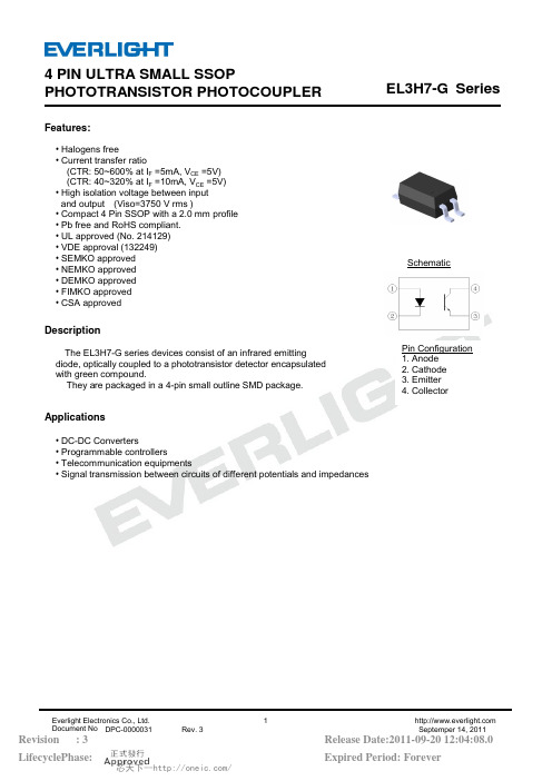
4 PIN ULTRA SMALL SSOP PHOTOTRANSISTOR PHOTOCOUPLER
Transfer Characteristics (Ta=25°C unless specified otherwise)
Parameter Collector-Emitter saturation voltage Isolation resistance Floating capacitance Rise time Fall time * Typical values at Ta = 25°C Symbol VCE(sat) RIO CIO tr tf Min. 5×10 10
LOCTITE 242 产品说明书

技术数据表LOCTITE ®242®8.2018产品描述:®®LOCTITE® 5970专门设计用于法兰面的密封,其特有的配方性能在产品未固化时可以承受在线的低压测试。
其典型应用包括冲压金属盖板的密封,产品具有良好的耐油性,可以用于粘接面有相对位移的场合。
军事标准Mil-S-Mil-S-46163A 46163A LOCTITE ®242®符合军事标准Mil-S-46163A 要求.注意:这是一个区域性认可。
如需更多资料和说明请与当地的技术服务中心联系。
ASTM D5363在北美生产的每个批次抽检产品均按照第5.1.1与5.1.2段落中的总体要求以及第5.2中的详细规定进行测试固化前的材料特性比重@ 25°C 1.1闪点 -见MSDS粘度, Brookfield -RVF, 25°C,mPa.s (cp):转子 3#, 转速2rpm ≥5,000LMS转子 3#, 转速20rpm,Helipath 800至1,600LMS 布氏粘度, -RVT, 25°C,mPa.s (cp):转子 3#, 转速20rpm*900至1,400LMS光滑Lubricity,ASTM D5648,K value,ASTM D 5648,%:3/8x 16磷酸盐和油螺母、螺栓和钢垫圈。
Phosphate &Oil Nuts,Bolts,Steel Washer -10至10LMS (对于关键应用作业,必须对K 因素进行独立确定。
乐泰对单个紧固件上的产品特定性能表现不承担任何担保责任。
)典型固化特性固化速度与基材的关系固化速度取决于所用的基材.下图显示在不同材质的M10的螺栓和螺母上,破坏扭矩与时间的关系。
测试标准为ISO 10964标准.钢材上的强度 %固化时间10075502501min5min 10min30min 1h3h 6h 24h钢黄铜镀锌不锈钢固化速度与温度的关系固化速度取决于温度.下图显示在M10的螺栓和螺母上,在不同温度下破坏扭矩与时间的关系。
- 1、下载文档前请自行甄别文档内容的完整性,平台不提供额外的编辑、内容补充、找答案等附加服务。
- 2、"仅部分预览"的文档,不可在线预览部分如存在完整性等问题,可反馈申请退款(可完整预览的文档不适用该条件!)。
- 3、如文档侵犯您的权益,请联系客服反馈,我们会尽快为您处理(人工客服工作时间:9:00-18:30)。
X200 SERIES (CMOS)
STANDARD SPECIFICATIONS
FREQUENCY RANGE
1.5 Hz to 12 MHz FREQUENCY ACCURACY @ + 25 o
C + 0.0015% ( + 15 PPM )FREQUECY STABILITY Vs. TEMPERATURE See Options Below OPERATING TEMPERATURE RANGE See Options Below INPUT VOLTAGE ( See note below ) + 5 VDC to + 15 VDC + 10% INPUT CURRENT
5 mA Max. @ + 5 VDC
25 mA Max. @ + 15 VDC
OUTPUT CMOS
LOAD 200 K Ω in parallel with 50 pf SYMMETRY 60/40% @ 50% Output Level RISE & FALL TIMES
150 nS Max. @ + 5 VDC ( 10% to 90% Output Level )
50 nS Max. @ + 15 VDC
START-UP TIME
< 10 MHz 20 mS Max.> 10 MHz
15 mS Max.
FREQUENCY STABILITY Vs. VOLTAGE
+ 0.0005% ( + 5 PPM ) Max.
( for 10% change in Voltage )
AGING @ +25 o
C
+ 0.0005% ( + 5 PPM ) / year Max.
Contact Xsis Engineering for special requirements such as, Output Symmetry, Start-up Time, Frequency Accuracy,
Complementary Outputs, Multiple Outputs, etc.
ORDERING INFORMATION ( Select from options below ) :
FREQUENCY
2Frequency Stability 1 = + 0.1%2 = + 0.05%3 = + 0.01%4 = + 0.005%5 = + 0.002% *
* Option 5 not available for - 55 o C to +125 o C
EXAMPLE: X243 - 883B - 4.000 MHz = 14 Pin Package with “X” Pinout, CMOS, + 0.005% over
-55 o
C to +125 o
C, Mil-Screened , and 20.000 MHz
1 = 0 o
C to + 70 o
C
2 = - 30 o C to + 85 o
C
3 = - 55 o C to +125 o
C
Operating Temperature Range Add Suffix “883B” for Mil-Screened Option
Xsis Electronics, Inc. 12620 W. 63rd St., Shawnee, KS 66216 Tel. 913-631-0448 Fax. 913-631-1170 email xsis@
05/00
X Pin Connections 14 B+
7 GND 8 OUTPUT All Others N/C
( Similar to M55310/18 )
PACKAGE, SEAL & LEAD FINISH Conforms with the Requirements of MIL-PRF-55310
Note: Input Voltage must be specified for 200 Series CMOS parts, minimum input voltage required depends upon
output frequency and operating temperature range. Consult factory for your specific application.
Pin 1 is identified with a Sq. Corner 0.105”0.095”0.250”0.200”0.020”0.016”
0.200” Max.0.305”
0.295”
0.305”
0.295”0.507” Max.
0.254” Max.0.439” Max.
0.605”0.595”0.877” Max.
0.155”0.145”17
8
14。