1S1886中文资料
RAiO RA8816N 144x65 字符 图形液晶驱动器规格说明书

RA i ORA8816N144x65 Character / GraphicLCD DriverSpecificationVersion 1.2June 02, 2011RA i O Technology Inc.@Copyright RaiO Technology Inc. 2011Update HistoryVersion Date Description 1.0 January 03, 2011 Preliminary edition1.1 May 17, 2011 1. Revise REG[12h] of Table 5-1 and relative descriptions.2. Add Section 6-2 : N-line Inversion.May 23, 2011 1. Add the description of REG[19h].2. Remove IIC relative descriptions.1.2June 2, 2011 1. Add maximum sleep mode current in Table 9-2.Chapter Contents Page1.General Description (5)2.Feature (5)3.Block Diagram (6)4.Pin Definition (7)4-1MPU Interface (7)4-2Clock and Power (8)4-3LCD Panel Interface (8)4-4Misc (9)5.Registers Description (10)5-1Register Table (10)5-2Register Contents (11)6.Function Description (24)6-1MPU Interface (24)6-1-1Parallel Interface (24)6-1-2Serial Interface (25)6-1-3Register Read/Write (27)6-1-4Memory Read/Write (29)6-2N-Line Inversion (31)6-3Memory (32)6-4System Clock (33)6-5LCD Driver and Power Circuit (33)6-5-1Booster Circuit (34)6-5-2Voltage Regulator (35)6-5-3Voltage Follower (36)6-5-4LCD Driver (37)6-6Interrupt (37)6-7Key-Scan (38)6-8I/O Port (39)6-9ASCII Block (39)6-10P ower Control (40)7.Display Functions (41)7-1Text Mode (41)7-2Graphic Mode (41)7-3Cursor Setting (42)7-3-1Cursor Position and Shift (42)7-3-2Cursor Display and Blink (42)7-3-3Cursor Height (43)7-4Display Window (43)7-5Horizontal Scroll (44)7-6Vertical Scroll (45)8.Pin Diagram (47)8-1COG Pad (47)8-2Pad X/Y Coordinate (49)9.Electrical Characteristic (54)9-1Absolute Maximum Ratings (54)9-2DC Characteristic (54)9-3Timing Characteristic (55)9-3-1Parallel Interface (55)9-3-2Serial Interface (57)9-3-3Reset Interface (60)Appendix A. COG Technical Parameter (61)Appendix B. BIG-5 Font Code Table (66)Appendix C. GB Font Code Table (73)Appendix D. S-JIS Font Code Table (95)1. General DescriptionThe RA8816N is a Dot-Matrix LCD Driver that supports both character and graphic modes. It has a built-in 256K bytes character ROM and 1170 bytes display RAM. The embedded ROM consists of Chinese (or Japanese for –J product), English and ASCII fonts, and the embedded display RAM supports up to 144x65 dots LCD panel. The RA8816N also provides a scrolling buffer memory for scrolling functions. It supports vertical and horizontal scrolling features, and all of these functions are executed by hardware.In character mode, the RA8816N supports Traditional Chinese (BIG5), Simplified Chinese (GB) and Japanese (S-JIS) code. The system (MPU) does not need to take a lot of time to show the Chinese or Japanese font in this mode. It also provides small ASCII (8x8) and big ASCII (8x16) fonts for English, Japanese, European and Latin character. The RA8816N also integrates much powerful hardware that includes contrast adjustment, 4x5 Key-Scan and eight General Purpose I/Os.The RA8816N is a highly integrated chip of LCD controller and driver. It reduces a lot of time for system development, and saves much cost for hardware system that due to it provides many features for related LCD display applications.2. FeatureSupport both Character and Graphic Mode Support 8080 / 6800, 8 / 4-bit Parallel Interface, 3-Wire / 4-Wire Serial InterfaceBuilt-in 256KB Font ROM: Chinese, S-JIS, English, ASCII, Japanese, Latin, Latin-ext A, Latin-ext BSupport ASCII 8x8 / 8x16 Half Size Font, 16x16 Full Size Chinese FontSupport Maximum 144 SEG x 65 COM LCD Panel. 4 x 9 Chinese Fonts (16x16), or 8 x 18 English Fonts (8x8)Built-in 256 bytes SRAM for Create Font Built-in 1170 bytes Display RAM and 450 bytes Scrolling BufferSupport 1/65 Duty, 1/9~1/5 Bias PanelBuilt-in 2X~4X (Voltage Booster), Voltage Regulator, Voltage FollowerEight General Purpose I/Os (GPIO)Built-in 4x5 Key-scan CircuitSupport Horizontal / Vertical Scrolling FunctionsProvide 32-Steps Contrast AdjusterBuild-in RC OscillatorVoltage Operation: VDD Æ 2.7~3.6VPackage: Gold Bump DieTable 2-1 : Ordering InformationParts Number Package and Font TypeRA8816N-T Au-Bump Die, Traditional Chinese (BIG5) RA8816N-S Au-Bump Die, Simplified Chinese (GB2312) RA8816N-J Au-Bump Die, Japanese (S-JIS)3. Block DiagramFigure 3-1 : System BlockThe RA8816N is consisted of Display RAM, 256KB Font ROM, Command Registers, LCD Controller,LCD Driver, Voltage Booster, Voltage Regulator, MPU Interface and Key-Scan circuit.C[3:1]P C[2:1]M V0~V4 VOUT SEG0~SEG143 COM0~COM63 COMS_ACOMS_BDB[7:0]RD(EN)WR(R/W)CS D/C(RS)C86BIT4P/S KST[3:0]KIN[4:0]INTIO[7:0]CLK_SEL EXT_CLK RST TEST[2:0]TP[6:0]VR VREFFigure 3-2 : Internal Block4. Pin Definition4-1 MPU InterfaceTable 4-14-2 Clock and PowerTable 4-2Pin NameI/ODescriptionV0~V4 O Voltage Source of LCD DriverThe relationship of the power is VOUT>V0≧V1≧V2≧V3≧V4≧VSSC[3:1]P, C[2:1]N I Capacitor InputThese are used to connect capacitors for internal Booster.VOUT OBooster Output VREF I Reference Voltage InputThis is the external reference voltage input when the internal one isdisabled.VR IVoltage AdjustmentApplies voltage between V0 and VSS by connecting a resistor divider. CLK_SEL IClock SelectThis pin is used to select the clock source. When CLK_SEL is “1”, theclock is generated by internal RC oscillator. When CLK_SEL is “0”, the system clock is driven by external pin - EXT_CLK. EXT_CLK I External ClockWhen CLK_SEL is “0”, this pin is the external clock input. When CLK_SELis “1”, this pin is not used and has to be connected to VDD or GND.VDDVDDPP Power GNDGNDPP Ground4-3 LCD Panel InterfaceTable 4-3Pin NameI/ODescriptionSEG0 ~ SEG143 O Segment Signals for PanelCOM0 ~ COM63O Common Signals for Panel COMS_A COMS_B O Icon Common Signals for Panel DUMY[5:0]ODummy PAD4-4 Misc.Table 4-4Table 4-5: Pin Definition of Parallel / Serial Mode of MPUNote1 : “--" means the pin is not used and kept floating (NC).Note2 : In serial mode, the unused parallel pins have to be connected to high (VDD).5. Registers Description5-1 Register TableTable 5-1 : Register TableID Name D7 D6 D5 D4 D3D2 D1 D0 Description0 DWFR B/C -- NW5 NW4 NW3 NW2 NW1 NW0 Wave Form Select1 PWRR SRST MCLR-- IO_IENKWK IOWK DOFF_Z SLP Power Control 2 SYSR LS3 LS2 LS1 LS0 FONT1FONT0RS1 RS0 System Setting3 MWMR BMOD1 BMOD0 BIENASCSBOLDINVMD1MD0Memory Mode 4 CURCR H3 H2 H1 H0 -- BLK CRCUR_ENCursor Control5 X-CUR -- -- X5 X4 X3 X2 X1 X0 Cursor X Position6 Y-CUR -- Y6 Y5 Y4 Y3 Y2 Y1 Y0 Cursor Y Position KEYR KSB KDB1 KDB0 KSTB_S EL K_AUTOIRE KF1/ KSTB1KF0/KSTB0 Key-scan ControlSIRQ KSTB1 KSTB0KSD4KSD3KSD2KSD1KSD07KSDRSIRQ AKD6 AKD5 AKD4AKD3AKD2AKD1AKD0Key-scan Data8SWSXR -- -- -- SSX4SSX3SSX2SSX1SSX0 X-Scroll Start 9 SWSYR -- -- SSY5 SSY4SSY3SSY2SSY1SSY0 Y-Scroll Start A SWRXR -- -- -- SRX4SRX3SRX2SRX1SRX0 X-Scroll Range B SWRYR PINV -- SRY5 SRY4SRY3SRY2SRY1SRY0 Y-Scroll Range C SCOR SL7 SL6 SL5/SR5SL4/SR4SL3/SR3SL2/SR2SL1/SR1SL0/SR0 Scroll UnitD ASCR SPD3 SPD2 SPD1 SPD0STP3STP2STP1STP0 Auto Scroll ControlESCCRSCR_IM D1 SCR_IM D0 SCR_M DSBUFSCR_DI R1 SCR_DI R0 SCR_IN TEN AUTO_SCRScroll Control F ISRBF -- -- -- IO_I SCR_I KI BI Interrupt Status 10 CSTRBR2 BR1 BR0 CT4 CT3 CT2 CT1 CT0 Contrast 11 DRCR_A BOFF EN_R EN_G ROFFIDIR -- CDIR SDIR Driver Control 12 DRCR_B CK_BS1 CK_BS0 RR2 RR1 RR0 IRS -- -- Driver Control13 BLTR BLK_EN PBK_EN --INV BLT3BLT2BLT1BLT0 Blink Setting 14 IODROE7 OE6 OE5 OE4 OE3 OE2 OE1 OE0 I/O Port Direction 15 IODAR IOD7 IOD6 IOD5 IOD4IOD3IOD2IOD1IOD0 I/O Port Data 17 CGMI-- -- -- -- -- UMI2UMI1UMI0 Create Font Select 18 CGMD CGMD7 CGMD6 CGMD5CGMD4CGMD3CGMD2CGMD1CGMD0 Create Font Data19 MISR-- -- -- -- -- -- -- EOR Misc Register5-2 Register ContentsThe RA8816N accepts two Command Cycle from MPU. One is Register Cycle (RS = 0) and the other one is Memory Cycle (RS = 1). MPU has to assign the register number of RA8816N before accesses these registers. Therefore, the first byte that MPU passes to RA8816N will be stored into Index Register and RA8816N will assume the next byte is read from or write into the register assigned by Index Register.IR (Index Register)RW RS DB7 DB6 DB5 DB4 DB3 DB2 DB1 DB00 0 0 0 0 ID4 ID3 ID2 ID1 ID0ID[4:0]: These bits are used to store the register number that MPU wants to access on next cycle.The ID[[4:0] provide 32 register numbers (00h~1Fh). But currently RA8816N only uses 25 registers (00h~18h). All of these registers are initialed to be “00h” after RESET.Memory Data (RAMD)RW RS DB7 DB6 DB5 DB4 DB3 DB2 DB1 DB0 0/1 1 D7 D6 D5 D4 D3 D2 D1 D0 If RS is “1”, it means MPU executes the Memory Cycle for the RA8816N. When RW is “0”, MPU will write data to Display or ICON RAM that according to the setting of MD[1:0] (bit1-0 of REG[03h]). For example, MPU writes Big5 / GB / ASCII code to memory in Text Mode, or write bitmap data to display memory in Graphic mode. When RW is “1”, the MPU reads data from different paths of RA8816N. It depends on the operation mode as following:1. F ull Size Text Mode: From up to down of left side (16 bytes), and then up to down of Right side (16bytes), total are 32 bytes.2. H alf Size Text Mode: From up to down, total 16 bytes data.3. S mall ASCII Text Mode: From up to down, total 8 bytes data.4. G raphics Mode: From left to right, each reading is one byte (8 Pixels).[00h] Driver Waveform Register (DWFR)RW DB7 DB6 DB5 DB4 DB3 DB2 DB1 DB00 B/C -- NW5 NW4 NW3 NW2 NW1 NW0B/C: Select driver waveform type.0 Î B-Type waveform. AC drive waveform alternates in every frame.1 Î C-Type waveform. AC drive waveform is generated and alternates (n-line reversed AC drive)in each lines specified by NW5–NW0NW[5:0]: These bits are used to assign the Common (Line) number that internal frame signal changes state. The number n is set as NW + 1 for C-type function. For example, NW= 4, the AC drivewill alternate each 5 commons. This function is only supported when B/C is “1” (C-Typewave form). About the relative information, please refer to EOR description (REG[19h] Bit 0)and Section 6-2 for detail description.[01h] Power Control Register (PWRR)RW DB7 DB6 DB5 DB4 DB3 DB2 DB1 DB0SLPDOFF_Z0 SRSTMCLR -- IO_IEN KWK IOWKSRST: S/W reset.0 Î No action.1 Î All of the registers will be initialed again except the display memory. Once this bit is set to 1then RA8816N has to take 50us for operation and cannot accept any new command fromMCU.MCLR: Memory clear.0 Î No action.1 Î Clear the Display RAM data to “00h”. Once this bit is set to 1 then RA8816N has to spend20ms for operation and cannot accept any new command from MCU. It is not allowed thatboth MCLR and SRST are set to ”1” or MCLR will be no effect.IO_IEN : I/O port interrupt setting.0 Î Disable.1 Î Enable.KWK: Key-scan wakes up setting.0 Î Disable.1 Î Enable.IOWK: I/O port wakes up setting.0 Î Disable.1 Î Enable.DOFF_Z: Display off.0 Î LCD driver and display off.1 Î LCD driver and display on.SLP: Sleep mode setting.0 Î RA8816N wakes up.1 Î Enter sleep mode, and disable the clock. This bit will be cleared to “0” when wake up signalis from I/O port or Key-scan.[02h] System Register (SYSR)RW DB7 DB6 DB5 DB4 DB3 DB2 DB1 DB00 LS3 LS2 LS1 LS0 FONT1FONT0RS1 RS0LS[3:0]: Set the segment number. The maximum segment of RA8816N is 144.Table 5-2LS3 LS2LS1LS0Line No.0 0 0 0 160 0 0 1 320 0 1 0 480 0 1 1 640 1 0 0 800 1 0 1 960 1 1 0 1120 1 1 1 1281 0 0 0 144:Reserved:1 1 1 1 ReservedFONT[1:0]: Set font code mapping.00 Î BIG-5, 10 Î GB2312, X1 Î S-JIS.RS[1:0]: Set the common number. The maximum common of RA8816N is 64 (Not including Icon).Table 5-3Common Output PadsDuty RS1 RS0 Status COM[0-15]COM[16-23]COM[24-26]COM[27-36]COM[37-39]COM[40-47]COM[48-63]COMSNormal COM[0-15]NCCOM[16-31]1/33 0 0ReverseCOM[31-16]NCCOM[15-0]COMSNormal COM[0-23] NC COM[24-47] 1/49 0 1Reverse COM[47-24] NC COM[23-0]COMSNormal COM[0-26] NC COM[27-53]1/55 1 0Reverse COM[53-27] NC COM[26-0]COMSNormal COM[0-63]1/65 1 1Reverse COM[63-0]COMS[03h] Memory Write Mode Register (MWMR)RW DB7 DB6 DB5 DB4 DB3 DB2 DB1 DB00 BMOD1BMOD0 BIEN ASCS BOLD INV MD1 MD0 BMOD[1:0]: Set the range for memory written.Table 5-4BMOD1 BMOD0 Memory Range of Write0 0 Normal Display Range0 1 Display Range + Scroll-Buffer1 xScroll-BufferBIEN: Busy interrupt control.0 Î Disable.1 Î Enable (After write data to memory).ASCS: Select BIG ASCII Table.0 Î Select ASCII Table-1.1 Î Select ASCII Table-2. (Refer to Ch. 6-9)BOLD: Select Bold Font to write into Display RAM.0 Î Normal font.1 Î Bold font.INV: Select inverse font to write into Display RAM.0 Î Normal font.1 Î Inverse font.MD[1:0]: Select operation mode for Display RAM.Table 5-5MD1 MD0OperationMode0 0 GraphicMode0 1 SmallASCII(8X8)1 0 BigASCII(8X16)1 1 Full Size (16X16)In Full-Size mode (MD[1:0] = 11), if the first byte data is less than 80h, the RA8816N will assume it is an ASCII code and show the Big ASCII font. But if want to show the Big ASCII font that code is larger than 80h, then the operation mode has to be changed to Big ASCII mode (MD[1:0] = 10).[04h] Cursor Control Register (CURCR)RW DB7 DB6 DB5 DB4 DB3 DB2 DB1 DB0CUR_EN0 H3 H2 H1 H0 -- BLK CRH[3:0]: Set the cursor height.Table 5-6(Pixel)H3 H2H1H0Height0 0 0 0 10 0 0 1 20 0 1 0 30 0 1 1 40 1 0 0 50 1 0 1 60 1 1 0 70 1 1 1 81 0 0 0 91 0 0 1 101 0 1 0 111 0 1 1 121 1 0 0 131 1 0 1 141 1 1 0 151 1 1 1 16In Small ASCII mode (8X8), the H3 is reserved. The setting of cursor height is only form 1~8 pixels (H[3:0] = x000b ~ x111b).BLK: Cursor blink select.0 Î No blinking.1 Î Cursor blinking.CR: Cursor return.0 Î No action.1 Î Cursor return. Cursor will return to the left of panel.CUR_EN: Cursor display select.0 Î Cursor hides.1 Î Cursor displays.[05h] Cursor Position Register of X (X-CUR)RW DB7 DB6 DB5 DB4 DB3 DB2 DB1 DB00 -- -- X5 X4 X3 X2 X1 X0X[5:0]: Set the cursor position on segment. The unit is 8 pixels. Because the maximum segment of the RA8816N is 144-pixels, therefore the range of X[5:0] is 0~11h. When the X[5:0] is 20h or 21h, then the cursor position is assign to horizontal scroll buffer.[06h] Cursor Position Register of Y (Y-CUR)RW DB7 DB6 DB5 DB4 DB3 DB2 DB1 DB00 -- Y6 Y5 Y4 Y3 Y2 Y1 Y0Y[6:0]: Set the cursor position on common. The unit is 1 pixel. Because the maximum common of theRA8816N is 64-pixels, therefore the range of Y[6:0] is 0~3Fh. When the Y[6:0] is 40h~4Fh,then the cursor position is assign to vertical scroll buffer. When it is 50h then the cursor islocated at COMS (Icon).[07h] Key-scan Control Register (KEYR) (Write Only)RW DB7 DB6 DB5 DB4 DB3 DB2 DB1 DB00 KSB KDB1 KDB0 KSTB_SE L K_AUTO IRE KF1/ KSTB1 KF0/ KSTB0KSB: Key-scan control.0 Î Disable key-scan.1 Î Enable key-scan.KDB[1:0]: Set the de-bounce time of key-scan in auto mode. The one time means one loop ofkey-scan.Table 5-7KDB1 KDB0 Times0 0 80 1 161 0 321 1 64KSTB_SEL: In manual mode,0 Î The DB[1:0] are defined as KF[1:0].1 Î The DB[1:0] are defined as KSTB[1:0]. In auto mode, the DB[1:0] is also defined as KF[1:0].K_AUTO: Set the scan mode.0 Î Manual Mode. The RA8816N will not store the code into AKD[6:0]. MPU has to read datafrom KSTB[1:0] and KSD[4:0] to make sure which key is pressed. Of course, MPU couldknow if not only one key is pressed at the same time in manual mode.1 Î Auto Mode. The RA8816N will auto detect the key-pressed event and store the code intoAKD[6:0] for MPU reading.IRE: Set the interrupt of key-scan.0 Î Hardware interrupt is disabled while key is pressed.1 Î Generate hardware interrupt while key is pressed.KF[1:0]: Set the frequency of Key-scan.Table 5-8KF1 KF0 Pulse Width Key-scan Cycle Time (4x5)0 0 256us1.024ms 0 1 512us2.048ms 1 0 1.024ms4.096ms 1 1 2.048ms9.182msKSTB[1:0]: In manual mode, These two bits are used to set the strobe for the Row of key matrix. Ifkey-pressed event is occurred, MPU can read data from KSTB[1:0] and KSD[4:0] tomake sure which key is pressed. The strobe data are also readable from Bit[6:5] ofregister KSDR.[07h] Key-scan Data Register (KSDR) (Read Only)If K_AUTO = 0:RW DB7 DB6 DB5 DB4 DB3 DB2 DB1 DB01 SIRQ KSTB1 KSTB0KSD4 KSD3 KSD2 KSD1 KSD0 SIRQ: Indicate the interrupt of key-scan. This bit is cleared when bit 1 of REG[0Fh] is written “0”. KSTB[1:0]: These two bits show which pin of KST[3:0] is active.KSD[4:0]: KIN return data. These bits are used in manual mode. MPU can read data from KSTB[1:0] and KSD[4:0] to make sure which key is pressed.If K_AUTO = 1:RW DB7 DB6 DB5 DB4 DB3 DB2 DB1 DB01 SIRQ AKD6 AKD5 AKD4 AKD3 AKD2 AKD1 AKD0 SIRQ: Indicate the interrupt of key-scan. This bit is cleared when bit 1 of REG[0Fh] is written “0”.AKD[6:0]: Scan Data (Code). In auto mode, MPU reads data from this register to know the status of key matrix. The RA8816N supports 4x5 key matrix -- total 20 keys. The BCD number of00h~09h and 10h~19h are mapping to these keys.Table 5-9DataAKD[6:0] Scan00h~19h Key No. Input20h~39h Long Key No. InputRelease42h KeyOther Reserved[08h] Scroll Window Start X Register (SWSXR)RW DB7 DB6 DB5 DB4 DB3 DB2 DB1 DB00 -- -- -- SSX4 SSX3 SSX2 SSX1 SSX0SSX[4:0]: Set Segment (X) start point of scroll window. The unit is half size width (8 pixels).[09h] Scroll Window Start Y Register (SWSYR)RW DB7 DB6 DB5 DB4 DB3 DB2 DB1 DB00 -- -- SSY5 SSY4 SSY3 SSY2 SSY1 SSY0SSY[5:0]: Set the Common (Y) start point of scroll window. The unit is one pixel.[0Ah] Scroll Window Range X Register (SWRXR)RW DB7 DB6 DB5 DB4 DB3 DB2 DB1 DB00 -- -- -- SRX4 SRX3 SRX2 SRX1 SRX0SRX[4:0]: Set Segment (X) offset of scroll window. The unit is half size width (8 pixels).[0Bh] Scroll Window Range Y Register (SWRYR)RW DB7 DB6 DB5 DB4 DB3 DB2 DB1 DB00 PINV-- SRY5 SRY4 SRY3 SRY2 SRY1 SRY0PINV : Inverse area select.0 Î Whole screen inverse.1 Î Partial screen inverse.The function should be considered with bit 4 of BLTR (REG[13h]).SRY[5:0]: Set the Common (Y) offset of scroll window. The unit is one pixel.[0Ch] Scroll Offset Register (SCOR)RW DB7 DB6 DB5 DB4 DB3 DB2 DB1 DB0SL0/SR0SL5/SR5SL4/SR4SL3/SR3SL2/SR2SL1/SR10 SL7 SL6SL[7:0]: Set the shifted unit of horizontal scroll. The unit is one pixel and active when register SCR_MD (bit 5 of REG[0Eh]) is cleared to “0”.SR[5:0]: Set the shifted unit of vertical scroll. The unit is one pixel and active when register SCR_MD (bit 5 of REG[0Eh]) is set to “1”.In auto scroll mode, this register is also used to set the Common or Segment start position of scroll.In manual scroll mode, the shifted unit of this register cannot over the range of scroll area defined in REG[08h~0Bh].[0Dh] Auto-Scroll Control Register (ASCR)RW DB7 DB6 DB5 DB4 DB3 DB2 DB1 DB00 SPD3 SPD2 SPD1 SPD0 STP3 STP2 STP1 STP0SPD[3:0]: Set the speed of auto scroll.Table 5-10SPD3 SPD2SPD1SPD0ScrollTimeUnit0 0 0 0 10 0 0 1 3UnitsUnits0 0 1 0 5Units0 0 1 1 7Units0 1 0 0 17Units0 1 0 1 19Units0 1 1 0 21Units0 1 1 1 231 0 0 0 129UnitsUnits1 0 0 1 131Units1 0 1 0 1331 0 1 1 135UnitsUnits1 1 0 0 145Units1 1 0 1 147Units1 1 1 0 149Units1 1 1 1 1511 Unit = 1 Frame CycleSTP[3:0]: Set the shifted unit on auto scroll mode.Table 5-11STP3 STP2STP1STP0ShiftPixel0 0 0 0 10 0 0 1 20 0 1 0 30 0 1 1 40 1 0 0 50 1 0 1 60 1 1 0 70 1 1 1 81 0 0 0 91 0 0 1 101 0 1 0 111 0 1 1 121 1 0 0 131 1 0 1 141 1 1 0 151 1 1 1 16[0Eh] Scroll Control Register (SCCR)RW DB7 DB6 DB5 DB4 DB3 DB2 DB1 DB00 SCR_IMD1SCR_IMD0SCR_MD SBUFSCR_DIR1SCR_DIR0SCR_INTENAUTO_SCRSCR_IMD[1:0]: The definition is as following and they are available in auto scroll mode.0X: Set 1 pixel shift to caused interrupt (SCR_INTEN must be 1).10: Set 8 pixels shift to caused interrupt (SCR_INTEN must be 1)11: Set 16 pixels shift to caused interrupt (SCR_INTEN must be 1)SCR_MD: Scroll mode select.0 Î Manual scroll, the scroll offset is cleared to “0”.1Î Auto scroll mode.SBUF: Scroll-Buffer Control.0 Î Disable scroll buffer. The scroll area does not include the scroll buffer, only for display area.1 Î Enable scroll buffer. The scroll area includes the display area and scroll buffer.SCR_DIR[1:0]: Select the direction of scroll.Table 5-12SCR_DIR1 SCR_DIR0Direction of Scroll0 0 Left to Right (Horizontal)0 1 Right to Left (Horizontal)1 0 Up to Down (Vertical)1 1 Down to Up (Vertical)SCR_INTEN: Set the scroll interrupt.0 Î Disable scroll interrupt.1 Î In auto scroll mode, when scrolling 1, 8 or 16 pixels generate an interrupt to MPU.AUTO_SCR: Auto-Scroll control.0 Î Stop the Auto-Scroll. If want to stop the auto scroll mode or display new data on the screen,then the bit5 of SCR_MD must be cleared to 0 first.1 Î Auto-Scroll is enabled.[0Fh] Interrupt Status Register (ISR)RW DB7 DB6 DB5 DB4 DB3 DB2 DB1 DB0SCR_I KI BI1 BF -- -- -- IO_IBF: Busy flag.0 Î Display RAM is idle (Write complete).1 Î Display RAM is in busy (Data Write).IO_I: I/O port interrupt.0 ÎNo I/O port interrupt.1 Î Interrupt for I/O port.SCR_I: Scroll interrupt.0 Î No scroll Interrupt.1 Î Interrupt for scroll is completedKI: Key-scan interrupt.0 Î No key pressed Interrupt.1 Î Interrupt for key pressed.BI: Busy interrupt.0 Î No busy Interrupt1 Î Interrupt for the event of writing data to display RAM is completed.[10h] Contrast Adjust Register (CSTR)RW DB7 DB6 DB5 DB4 DB3 DB2 DB1 DB00 BR2 BR1 BR0 CT4 CT3 CT2 CT1 CT0BR[2:0]: Set the LCD Bias(Base on 144x65).Table 5-13BR2 BR1 BR0 Bias0 0 0 1/50 0 1 1/60 1 0 1/70 1 1 1/81 0 0 1/91 0 1 1/91 1 0 1/91 1 1 1/9CT[4:0]: Set the Contrast (32 Levels). Normally it depends on the liquid crystal, power and panel size to adjust the best display quality.Table 5-14CT4 CT3 CT2CT1CT0Contrast0 0 0 0 0 Light0 0 0 0 1::1 1 1 1 1 Dark[11h] Driver Control Register1 (DRCR_A)RW DB7 DB6 DB5 DB4 DB3 DB2 DB1 DB0ROFF IDIR -- CDIR SDIREN_G0 BOFF EN_RBOFF: Booster control.0 Î Disable internal booster and use the external voltage.1 Î Enable internal booster.EN_R: Reference voltage control.0 Î Disable the internal reference voltage circuit and the regulator uses external one.1 Î Enable internal reference voltage circuit for regulator using.EN_G: Regulator control.0 Î Use external power for V0. EN_R and BOFF have to be cleared to “0” (Off) to reduce powerconsumption.1 Î The LCD bias V0 is generated by internal regulator.ROFF: Voltage Follower control.0 Î Disable internal Voltage Follower, and use external voltage to generate LCD Bias voltage. Ifuse external Voltage Follower, then EN_G, EN_R and BOFF have to be cleared to “0” (Off)to reduce power consumption.1 Î Internal Voltage Follower is enabled for LCD Bias voltage.IDIR : Icon sequence select.0 Î Icon sequence is fixed.1 Î Icon sequence follow the setting of CDIR / SDIR.CDIR: Common sequence select.0 Î Pins COM0~63 are mapping to Common 0~63.1 Î Pins COM0~63 are mapping to Common 63~0.SDIR: Segment sequence select.0 Î Pins SEG0~143 are mapping to Segment 0~143.1 Î Pins SEG0~143 are mapping to Segment 143~0.[12h] Driver Control Register (DRCR_B)RW DB7 DB6 DB5 DB4 DB3 DB2 DB1 DB0CK_BS0 RR2 RR1 RR0 IRS -- --0 CK_BS1CK_BS[1:0]: Select the clock of Booster. Assume that the RC oscillator clock is 100KHz.Table 5-15CK_BS1 CK_BS0Clock of Booster0 0 SYS_CLK/2 Æ 50KHz0 1 SYS_CLK/4 Æ 25KHz1 0 SYS_CLK/6 Æ 16.7KHz1 1 SYS_CLK/8 Æ 12.5KHzRR[2:0]: Set the Resistor Ratio of Regulator. The ratio is V0. : V REF. Please refer to Ch. 6-5-2.Table 5-16RR2 RR1RR0Resistor Ratio0 0 0 X30 0 1 X3.50 1 0 X40 1 1 X4.51 0 0 X51 0 1 X5.51 1 0 X61 1 1 X6.4IRS: Select the resistors for the V0 voltage level adjustment.0 Î Do not use the internal resistors. The V0 voltage level is regulated by an external resistorvoltage divider that is attached to the VR signal.1 Î Use the internal resistors.[13h] Blink Timer Register (BLTR)RW DB7 DB6 DB5 DB4 DB3 DB2 DB1 DB0PBK_EN -- INV BLT3 BLT2 BLT1 BLT00 BLK_ENBLK_EN: Blinking function.0 Î Off.1 Î On.PBK_EN: Whole or partial screen blinking selection.0 Î Whole screen.1 Î Partial screen. The blinking area depends on the scroll window. It means the partial area isset by register SWSXR, SWSYR, SWRXR and SWRYR. When the partial blinking is off, theabove four registers had better to be cleared to 0. Note, only BLK_EN is set to “1” when blinkis active.INV: Set display inversely.0 Î Normal display.1 Î Display inversely. The inverse area depends on the bit7 (PINV) of register SWRYR.BLT[3:0]: Set blinking time.Table 5-17BLT3 BLT2BLT1BLT0Blink Time (Unit: Frames)0 0 0 0 80 0 0 1 160 0 1 0 240 0 1 1 320 1 0 0 400 1 0 1 480 1 1 0 560 1 1 1 641 0 0 0 721 0 0 1 801 0 1 0 881 0 1 1 961 1 0 0 1041 1 0 1 1121 1 1 0 1201 1 1 1 128[14h] I/O Direction Control Register (IODR)RW DB7 DB6 DB5 DB4 DB3 DB2 DB1 DB00 OE7 OE6 OE5 OE4 OE3 OE2 OE1 OE0OE[7:0]: Select the I/O port direction.0 Î Input.1 Î Output.[15h] I/O Data Register (IODAR)RW DB7 DB6 DB5 DB4 DB3 DB2 DB1 DB00 IOD7 IOD6 IOD5 IOD4 IOD3 IOD2 IOD1 IOD0IOD[7:0]: This register stores the input / output data of I/O port when it is in input / output mode.[17h] CGRAM Register (CGMI)RW DB7 DB6 DB5 DB4 DB3 DB2 DB1 DB00 -- -- -- -- -- UMI2UMI1UMI0 UMI[2:0]: Select the create font number. The RA8816N allows user to create eight 16x16 full size fonts.The mapping font code is FFF0h~FFF7h.。
SNLS系列芯片名称
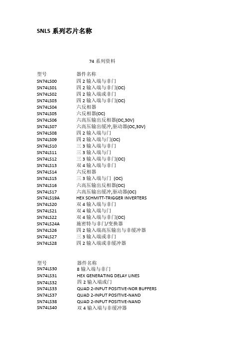
SNLS系列芯片名称74系列资料型号器件名称SN74LS00 四2输入端与非门SN74LS01 四2输入端与非门(OC)SN74LS02 四2输入端或非门SN74LS03 四2输入端与非门(OC)SN74LS04 六反相器SN74LS05 六反相器(OC)SN74LS06 六高压输出反相器(OC,30V)SN74LS07 六高压输出缓冲,驱动器(OC,30V)SN74LS08 四2输入端与门SN74LS09 四2输入端与门(OC)SN74LS10 三3输入端与非门SN74LS11 三3输入端与门SN74LS12 三3输入端与非门(OC)SN74LS13 双4输入端与非门SN74LS14 六反相器SN74LS15 三3输入端与门(OC)SN74LS16 六高压输出反相器(OC)SN74LS17 六高压输出缓冲,驱动器(OC)SN74LS19A HEX SCHMITT-TRIGGER INVERTERSSN74LS20 双4输入端与非门SN74LS21 双4输入端与门SN74LS22 双4输入端与非门(OC)SN74LS24A 施密特与非门/变换器SN74LS26 四2输入端高压输出与非缓冲器SN74LS27 三3输入端或非门SN74LS28 四2输入端或非缓冲器型号器件名称SN74LS30 8输入端与非门SN74LS31 HEX GENERATING DELAY LINESSN74LS32 四2输入端或门SN74LS33 QUAD 2-INPUT POSITIVE-NOR BUFFERS SN74LS37 QUAD 2-INPUT POSITIVE-NANDBUFFERSSN74LS38 QUAD 2-INPUT POSITIVE-NANDBUFFERSSN74LS40 双4输入端与非缓冲器SN74LS424线-10线译码器 SN74LS47BCD 七段译码,驱动器 SN74LS48BCD-TO-SEVEN-SEGMENT DECODERS/DRIVERS SN74LS49BCD-TO-SEVEN-SEGMENT DECODERS/DRIVERS SN74LS512路3-3输入,2路2-2输入与或非门 SN74LS544路2-3-3-2输入与或非门 SN74LS552路4-4输入与或非门 SN74LS56FREQUENCY DIVIDERS SN74LS57FREQUENCY DIVIDERS SN74LS68DUAL 4-BIT DECADE OR BINARY COUNTERS SN74LS69DUAL 4-BIT DECADE OR BINARY COUNTERS SN74LS73ADUAL J-K FLIP-FLOPS WITH CLEAR SN74LS74A双上升沿D 型触发器 SN74LS75QUAD BISTABLE LATCHES SN74LS76A单D 型触发器 SN74LS78A双D 型触发器 型号器件名称 SN74LS854位数值比较器 SN74LS86A四二进制原码/反码,0/1单元 SN74LS90DECADE COUNTER SN74LS918位移位寄存器 SN74LS92DIVIDE-BY-TWELVE DECADECOUNTER SN74LS934-BIT BINARY COUNTERS SN74LS95B4位移位寄存器 SN74LS96四2输入端与非门 SN74LS107A双 J-K 触发器 SN74LS109A4位移位寄存器 SN74LS112A双下降沿J-K 触发器 SN74LS114A双 J-K 触发器 SN74LS122RETRIGGERABLE MONOSTABLEMULTIVIBRATOR SN74LS123可重触发双稳态触发器 SN74LS125A四总线缓冲器 SN74LS126A四总线缓冲器 SN74LS132四2输入端与非门 SN74LS136QUAD 2-INPU T EXCLUSIVE-OR GATES 地址锁存,3线-8线译码器 3线-8线译码器 双2线-4线译码器SN74LS137SN74LS138SN74LS139ABCD-TO-DECIMAL DECODERS/DRIVERS 10线-4线优先编码器 8线-3线优先编码器 8选1数据选择器 双4选1数据选择器 双2线-4线译码器 双2线-4线译码器OC 四2选1数据选择器 四2选1数据选择器(反码输出) 十进制同步计数器4位二进制同步计数器 十进制同步计数器 4位二进制同步计数器 8位移位寄存器 8位移位寄存器 8位移位寄存器 4位二进制同步加/减计数器 4-BY-4 REGISTER FILES QUADRUPLE D-TYPE FLIP-FLOPS WITH CLEAR 4位D 型寄存器 六上升沿D 型发器 四上升沿D 型触发器 4位算述逻辑单元/函数生器 DUAL CARRY-SAFE FULL ADDERS 十进制加/减计数器 4位二进制加/减计数器 十进制加/减计数器(双时钟) 4位二进制加/减计数器(双时钟) 4位双向移位寄存器 4位移位寄存器 50/30/100-MHZ 可预置二-五-十进制计数器二-八-十六进制计数器 双单稳态触器 16 X 4 同步先入,先出存储器 16X4 SYNCHRONOUS FIFO MEMORY 16 X 4同步先入,先出存储器(OC ) 八反相缓冲/线驱动/线接收器 八缓冲/线驱动/线接收器 四总线收发器 四总线收发器 八缓冲/线驱动/线接收器 八双向总线发送/接发器4线-7段译码/高压输出驱动器SN74LS248 4线-7段译码/驱动器 SN74LS145SN74LS147SN74LS148SN74LS151SN74LS153SN74LS155ASN74LS156SN74LS157SN74LS158SN74LS160A SN74LS161ASN74LS162ASN74LS163ASN74LS164SN74LS165ASN74LS166ASN74LS169BSN74LS170SN74LS171SN74LS173ASN74LS174SN74LS175SN74LS181SN74LS183SN74LS190SN74LS191SN74LS192SN74LS193SN74LS194ASN74LS195ASN74LS196SN74LS197SN74LS221SN74LS222ASN74LS224ASN74LS227SN74LS228SN74LS240SN74LS241SN74LS242SN74LS243SN74LS244SN74LS245SN74LS247SN74LS251 8选1数据选择器SN74LS253 双4选1数据选择器SN74LS257B 四2选1数据选择器SN74LS258B 四2选1数据选择器SN74LS259B 8位可寻址锁存器SN74LS261 2 BY 4 BIT PARALLEL BINARY MULTIPLIER SN74LS266 QUAD 2-INPUT EXCLUSIVE-NOR GATESSN74LS273 八D触发器SN74LS279A QUAD /S-/R LATCHESSN74LS280 9位奇偶产生器/校验器SN74LS283 4位二进制超位全加器SN74LS290 ASYNCHRONOUS DECADE COUNTERSSN74LS292 可编程频率分配器/数字定时器SN74LS293 4-BIT 二进制计数器SN74LS294 可编程频率分配器/数字定时器SN74LS295B 4-BIT RIGHT-SHIFT LEFT-SHIFT REGISTERS SN74LS297 DIGITAL PHASE-LOCKED-LOOP FILTERSSN74LS298 QUADRUPLE 2-INPUT MULTIPLEXERSSN74LS299 8位双向通用移位/存储寄存器SN74LS320 CRYSTAL-CONTROLLED OSCILLATORSSN74LS321 CRYSTAL-CONTROLLED OSCILLATORSN74LS322A 8-BIT SHIFT REGISTERS WITH SIGN EXTEND SN74LS323 UNIVERSAL SHIFT / STORAGE REGISTERSSN74LS348 8线-3线优先编码器SN74LS352 双4选1数据选择器/多路(复用)器SN74LS353 双4选1数据选择器/多路(复用)器SN74LS354 8选1数据选择器/多路(复用)器/寄存器SN74LS355 8选1数据选择器/多路(复用)器/寄存器(OC)SN74LS356 8选1数据选择器/多路(复用)器/寄存器SN74LS365A 六总线驱动器SN74LS366A 六反相总线驱动器SN74LS367A 六总线驱动器SN74LS368A 六反相总线驱动器SN74LS373 六D型锁存器SN74LS374 六上升沿D型触发器SN74LS375 QUAD BISTABLE LATCHESSN74LS377 六上升沿D型触发器SN74LS378 HEX D-TYPE FLIP-FLOPSSN74LS379 QUAD D-TYPE FLIP-FLOPS算术逻辑单元/函数发生器 算术逻辑单元/函数发生器 8 BY 1 TWO'S-COMPLEMENT MULTIPLIERS QUAD SERIAL ADDERS/SUBTRACTORS 四2输入端异或门 双十进制计数器 双4位二进制计数器 CASCADABLE SHIFT REGISTERS OCTAL STORAGE REGISTERS QUADRUPLE 2-INPUT MULTIPLEXERS 可再触发单稳态多频振荡器 双可再触发单稳态多频振荡器 QUAD TRIDIRECTIONAL BUS TRANSCEIVERS QUAD TRIDIRECTIONAL BUS TRANSCEIVERS QUAD TRIDIRECTIONAL BUS TRANSCEIVERS QUAD TRIDIRECTIONAL BUS TRANSCEIVERS BCD-TO-DECIMAL DECODERS/DRIVERS QUADRUPLE BUS TRANSCEIVERS QUADRUPLE BUS TRANSCEIVERS OCTAL BUFFERS WITH 3-STATE OUTPUTS OCTAL BUFFERS OCTAL BUFFERS OCTAL BUFFERS ASYNCHRONOUS DECADE COUNTERS 8三态缓冲器(反相) OCTAL BUFFERS AND LINE DRIVERS 8-BIT BINARY COUNTERS 8-BIT BINARY COUNTERS 8-BIT BINARY COUNTERS 8-BIT BINARY COUNTERS SERIAL-IN SHIFT REGISTERS SERIAL-IN SHIFT REGISTERS SERIAL-IN SHIFT REGISTERS SERIAL-OUT SHIFT REGISTERS SHIFT REGISTERS WITH INPUT LATCHES 8-BIT SHIFT REGISTERS MEMORY REFRESH CONTROLLERS MEMORY REFRESH CONTROLLERS MEMORY REFRESH CONTROLLERS OCTAL 2-INPUT MULTIPLEXED LATCHES OSN74LS381ASN74LS382ASN74LS384SN74LS385SN74LS386ASN74LS390SN74LS393SN74LS395A SN74LS396SN74LS399SN74LS422SN74LS423SN74LS440SN74LS441SN74LS442SN74LS444SN74LS445SN74LS446SN74LS449SN74LS465SN74LS466SN74LS467SN74LS468SN74LS490SN74LS540SN74LS541SN74LS590SN74LS591SN74LS592SN74LS593SN74LS594SN74LS595SN74LS596SN74LS597SN74LS598SN74LS599SN74LS600ASN74LS601ASN74LS603ASN74LS604SN74LS606CTAL 2-INPUT MULTIPLEXED LATCHES OCTAL 2-INPUT MULTIPLEXED LATCHES 八总线收发器 八总线收发器 八总线收发器 电压控制振荡器 双电压控制振荡器 双电压控制振荡器 DUAL VOLTAGE-CONTROLLED OSCILLATORS 电压控制振荡器 双电压控制振荡器 16位平行误差检测修正电路 OCTAL BUS TRANSCEIVERS OCTAL BUS TRANSCEIVERS OCTAL BUS TRANSCEIVERS OCTAL BUS TRANSCEIVER/IOL=48MA 3-STATE OCTAL BUS TRANSCEIVERS OCTAL BUS TRANSCEIVERS OCTAL BUS TRANSCEIVERS OCTAL BUS TRANSCEIVERS OCTAL BUS TRANSCEIVERS AND REGISTERS OCTAL BUS TRANSCEIVERS AND REGISTERS OCTAL BUS TRANSCEIVERS AND REGISTERS OCTAL BUS TRANSCEIVERS AND REGISTERS OCTAL BUS TRANSCEIVERS AND REGISTERS OCTAL BUS TRANSCEIVERS AND REGISTERS OCTAL BUS TRANSCEIVERS AND REGISTERS SYNCHRONOUS UP/DOWN DECADE COUNTERS 可预置同步加减二进制计数器 4-BY-4 REGISTER FILES 4位通用移位寄存器/锁存器 4位通用移位寄存器/锁存器 SERIAL-IN SHIFT REGISTERS SERIAL-OUT SHIFT REGISTERS 4-BIT PARALLEL BINARY ACCUMULATOR 8位二进制或BCD 大小比较器 8位二进制或BCD 大小比较器 8位二进制或BCD 大小比较器 8-BIT MAGNITUDE/IDENTITY COMPARATORS 8位二进制或BCD 大小比较器 八位数据等值比较器 十进制同步计数器 二进制同步计数器 4位二进制同步计数器SN74LS607 SN74LS620 SN74LS621 SN74LS623 SN74LS624 SN74LS625 SN74LS626 SN74LS627 SN74LS628 SN74LS629 SN74LS630 SN74LS638 SN74LS639 SN74LS640 SN74LS640-1 SN74LS641 SN74LS642 SN74LS644 SN74LS645 SN74LS646 SN74LS647 SN74LS648 SN74LS649 SN74LS651 SN74LS652 SN74LS653 SN74LS668 SN74LS669 SN74LS670 SN74LS671 SN74LS672 SN74LS673 SN74LS674 SN74LS681 SN74LS682 SN74LS684 SN74LS685 SN74LS686 SN74LS687 SN74LS688 SN74LS690 SN74LS691 SN74LS693SN74LS696 SN74LS697 SN74LS699 同步加/减计数器4位二进制同步加/减计数器4位二进制同步加/减计数器。
psr661说明书

psr661说明书PSR60系列数字式综合测控装置技术说明书国电南京自动化股份有限公司GUODIAN NANJING AUTOMATION CO.,LTDPSR60系列数字式综合测控装置技术说明书编写审核批准V :1.1国电南京自动化股份有限公司2005年12月安全声明注意:对装置进行测试时,请使用可靠精确的测试仪进行测试。
有些模块的输入量程是通过板上跳线实现的,请在接线前仔细核对跳线,以免损坏模块。
危险:请不要用手触摸装置除机壳外的裸露带电部分和印制板上的器件管脚。
其他:出厂时,运行密码为1000,检修密码为2000,请用户重设。
请注意密码管理,以免由于越权使用密码,造成误操作。
版本声明本说明书适用于PSR60系列数字式综合测控装置主CPU 模块V1.49版本,详见下表。
1.软件本说明书对应的各模件最新版本号分别如下表:2.硬件初始版本。
产品说明书版本修改记录表* 技术支持电话:83537292传真:83537201* 本说明书可能会被修改,请注意核对实际产品与说明书的版本是否相符 * 005年12月第2版第1次印刷 * 国电南自技术部监制目录安全声明版本声明 1 概述 ................................................ ....................... 1 1.1 适用范围 ................................................ ................. 1. 性能特点 ................................................ ................. 技术参数 ....................................................................1 额定电气参数 ................................................ .............. 主要技术指标 ................................................ .............. 环境条件 ................................................ .................. 绝缘性能 ................................................ .................. 耐湿热性能 ................................................ ................ 电磁兼容性 ................................................ .............. 10. 机械性能 ................................................ ................ 10 装置硬件简介 ................................................ .............. 11.1 机箱结构 ................................................ ................ 11. 关于校准 ................................................ ................ 1 典型配置方案 .............................................................. 14.1 单模块类型定值简介 ................................................ ...... 14. 装置典型配置方案 ................................................ ........ 1 定值整定简介 ................................................ .............. 1 输入输出数据 ................................................ .............. 1 模块说明 ................................................ .................. 18.1 智能交流采集模块 ....................... 18.1.1 交流模块硬件说明 ................................................ ...... 18.1. 交流模块典型配置 ................................................ ...... 19.1. 交流模块定值及整定说明 ................................................2.1. 交流模块输入输出数据 ................................................ ..0. 管理主模块 ................................................ ..7.2.1 管理主模块硬件说....7.2. 管理主模块定值及整定说明 ..............................................8.2. 管理主模块输入输出数据 ................................................2. 电源模块 ................................................ .......5.3.1 电源模块硬件说明 ................................................ ......5. 智能开入模块 ................................................ ......5.4.1 开入模块硬件说明 ................................................ ......5.4. 开入模块典型配置 ................................................ ......6.4. 开入模块定值及整定说明 ................................................7.4. 开入模块输入输出数据 ................................................ ..1. 智能控制模块 ................................................ .....2.5.1 控制模块硬件说......2.5. 控制模块定值及整定说明 (3)PSRC1900系列微机式保护测控装置 PSRC1900系列保护控制自动化系统技术使用说明书杭州博瑞电气有限公司2012年2月目录1 概述 ................................................ . (1)1.1 产品特点 ................................................ ............................................... 1 1. PSRC1900系列装置分类 ................................................ ...................... 1 1. PSRC1900系列装置用途及主要功能 ................................................ .. 技术指....2.1 额定数据 ................................................ ................................................ 功率消耗 ................................................ ................................................ 过载能力 ................................................ ................................................ 测量及精度 ................................................ ............................................ 绝缘性能 ................................................ ................................................ 触点性能 ................................................ ................................................ 电磁兼容性 ................................................ ............................................ 环境条................................................ 应用标准 ................................................ ............................................... 装置硬件 ................................................ ....3.1 机械结构图 ................................................ ............................................ 电源插件 ................................................ ...................................... 操作插件 ................................................ ...................................... 遥信插件 ................................................ ...................................... 交流插件 ................................................ ...................................... CPU 板 ................................................ .................................................... 面板显示及操作说明 ..........................................4.1 面板显示 ................................................ ................................................ 菜单级别及说明 ................................................ .................................... 装置参数设定 ................................................ ..................................... 1 PSRC1910线路保护测控装置 . (14)5.1 基本配置及规格 ................................................ ................................. 14. 保护原理 ................................................ ............................................. 15. 定值设置 ................................................ ............................................. 15. 背板端子图111 ............................................... ................................... 18. 典型接线原理图 ................................................................................. 19. 保护逻辑框图 ................................................ .....................................1 PSRC1913线路自投保护测控装置 (2)6.1 基本配置及规格 ................................................ .................................6. 保护原理 ................................................ .............................................6. 定值设置 ................................................ .............................................6. 背板端子图 ................................................ .........................................6. 典型接线原理图 ................................................ .................................6. 保护逻辑框图 ................................................ ..................................... PSRC1920电容器保护测控装置 .. 07.1 基本配置及规 0机式保护测控装置7. 保护原理 ................................................ .............................................1. 定值设置 ................................................ .............................................2. 背板端子图 ................................................ .........................................3. 典型接线原理图 ................................................ .................................4. 保护逻辑框图 ................................................ ..................................... PSRC1950配变保护测控装置 . (7)8.1 基本配置及规格 ................................................ .................................8. 保护原理 ................................................值设置 ................................................ .............................................9. 装置背板端子图 ................................................ .................................0. 典型接线原理图 ................................................ .................................1. 保护逻辑框图 ................................................ ..................................... PSRC1960电动机保护测控装置 .. (4)9.1 基本配置及规格 ................................................ .................................9. 保护原理 ................................................ .............................................9. 定值设置 ................................................ .............................................6. 背板端子图 ................................................线原理图 ................................................ .................................9. 保护逻辑框图 ................................................ .....................................1 10 PSRC1982电压综合保护兼并列装置 (2)10.1 基本配置及规格 ................................................ ...............................10. 保护原理 ................................................ ...........................................10. 定值设置 ................................................ ...........................................10. 背板端子图 ................................................ .......................................10. 典型接线原理图 ................................................ ...............................10. 保护逻辑框图 ...................................................................................11 保护参考整定计算说明 ......................................1 用户安装调试说明 ..........................................1 通讯规约 ................................................ ..1 订货须知 ................................................ ..2PSRC1900系列微机式保护测控装置1 概述PSRC1900系列数字式保护测控装置是公司积累多年研发、生产数字式保护测控装置的基础上,经过大量的市场调研、配置方案论证所推出的面向35KV及以下电压等级的输配电元件及线路的保护、测量及控制系统。
超米克斯 电导胶与超米克斯 电导胶合金产品说明说明书

1US Headquarters TEL +(1) 781-935-4850FAX +(1) 781-933-4318 • Europe TEL +(44) 1628 404000FAX +(44) 1628 404090Asia Pacific TEL +(852) 2 428 8008FAX +(852) 2 423 8253South America TEL +(55) 11 3917 1099FAX +(55) 11 3917 0817Since 1961, Chomerics has invented and extended virtually every aspect of conductive elastomer materials technology —from the earliest silver and silver/copper filled silicones to the latest and more cost-effective silver/aluminum and nickel/graphite composites. Today we offer the most comprehensive selection and highest quality products available anywhere.Each conductive elastomer consists of a silicone,fluorosilicone, EPDM or fluorocarbon-fluorosilicone binder with a filler of pure silver, silver-plated copper, silver-plated aIuminum, silver-plated nickel, silver-plated glass, nickel-plated graphite, or unplated graphite particles.The development of these composites is the result ofdecades of research and testing, both in the laboratory and in the field. Our proprietary filler powder technology allows us to carefully control the composition, size, and morphology of the conductive particles. Their precise, uniform dispersion within the resinous binders produces materials with stable and consistent electrical and physical properties.Chomerics’conductive elastomers feature excellentresistance to compression set over a wide temperature range,resulting in years of continuous service. All meet MIL-STD-810requirements for fungus resistance. In addition to EMI shielding, these materials will provide an environmental or pressure seal if required.For those materials containing silver, both packaging and storage conditions should be similar to those for other silver-containing components, such as relays or switches. They should be stored in sheet plastic, such as polyester orpolyethylene, and kept away from sulfur-containing materials,such as sulfur-cured neoprene, cardboard, etc. To remove dirt,clean the elastomer with water or alcohol containing mild soap (do not use aromatic or chlorinated solvents).Table 3 on pages 5-7 outlines the properties and specification limits of Chomerics’conductive elastomers.These materials are produced in a virtually unlimited variety of molded, die-cut and extruded shapes and sizes Our Applications Engineering Department is veryaccessible, and ready to assist with material selection and gasket design. We welcome your inquiry.Material Selection Chomerics’array of conductive elastomers offers true flexibility in selecting the appropriate material for a specific application on the basis of cost and level of attenuation required. Price varies directly with shielding performance.For most applications, CHO-SEAL materials are preferred over CHO-SIL materials, owing to their superior physical properties and excellent shielding performance. With their reticulate structure, CHO-SIL materials are typically lighter in weight and more compressible.For military/aerospace applications, we recommend that users of conductive elastomer gaskets specify that materials meet the requirements of MIL-G-83528and be procured from MIL-G-83528 QPL sources. To avoid the risk of system EMI or environmental seal failure, any change in conductive elastomer seal supplier (includingMIL-G-83528 QPL suppliers) should be proceeded by thorough system qualification testing.Non-Silicone BaseElastomer Fluid Resistance Certain specialty elastomers (E6306, E6434, E6434E, V6433 and the various fluorosilicone based materials) are offered specifically for their fluid resistance properties. Table 1 shows the qualitative assessment of fluid resistance to various fluids for three non-silicone base elastomers used for Chomerics’conductive elastomers.3US Headquarters TEL +(1) 781-935-4850FAX +(1) 781-933-4318 • Europe TEL +(44) 1628 404000FAX +(44) 1628 404090Asia Pacific TEL +(852) 2 428 8008FAX +(852) 2 423 8253South America TEL +(55) 11 3917 1099FAX +(55) 11 3917 0817Conductive Elastomer Selection GuideThe chart on these pages provides selection guidelines for Chomerics’most general-purpose elastomer EMI gasket materials. With the exception of certain limitations noted under “Remarks”, all of these materials are electrically stable over time and provide excellent moisture and pressure sealing. They are all medium-durometer materials and differ mainly in shielding performance and corrosion resistance. (Silver-plated-aluminum filled materials aresignificantly more corrosion-resistant than silver-plated-copper and silver-plated-nickel filled materials. Refer to the discussion of CHO-SEAL 1298Corrosion-Resistant EMI Shielding Gasket on page 5.)Note on Gasket Deflection and Closure Force: We do NOTrecommend that material selection be based primarily on hardness. Unlike unfilled elastomers, hardness is not always a good indicator of deflection properties. Gasket shape is generally the most important determinant of deflection under load.For applications requiring large gasket deflection with minimum closure force, select a hollow strip configuration and/or evaluate the use of Chomerics’SOFT-SHIELD ®Low Closure Force Gaskets.5US Headquarters TEL +(1) 781-935-4850FAX +(1) 781-933-4318 • Europe TEL +(44) 1628 404000FAX +(44) 1628 404090Asia Pacific TEL +(852) 2 428 8008FAX +(852) 2 423 8253South America TEL +(55) 11 3917 1099FAX +(55) 11 3917 0817CHO-SEAL1298 Corrosion-ResistantEMI Shielding GasketCHO-SEAL 1298 elastomerincorporates unique particle plating and elastomer technology for increased corrosion resistance.When used in conjunction with the CHO-SHIELD 2000 series of corrosion-resistant conductive coatings on aluminum flanges, a corrosion-proof EMI flange system is obtained.CHO-SEAL 1298 gasket material is based on a silver-plated-aluminum filler dispersed in a fluorosiliconebinder, with corrosion inhibitingadditives that contain no chromates.It offers shielding effectiveness of 100 dB at 500 MHz and meets all requirements of MIL-G-83528 Type D (initial and aged). CHO-SEAL 1298gasket material also has excellent resistance to fluids and fuels commonly used in aviation and industrial applications.Corrosion Resistance Testing Chomerics has completedextensive corrosion resistance testing on CHO-SEAL 1298 gasket materialusing a gravimetric weight lossprocedure. A copy of the test method (CHO-TM 100) is available on request from Chomerics. T estfixtures and elastomer samples are also available. Contact Chomerics’Applications Engineering Department for further information.Lightning Strike ResistanceThe survivability of any system to lightning strike is dependent on specific flange design. Lightning strike testing of CHO-SEAL 1298gasket material has demonstrateda Copies of CEPS-0002 and CHO-TM-TP08 are available from Chomericsb Compression set is expressed as a percentage of deflection per ASTM D395 Method B., at 25% deflection. To determine percent recovery, subtract 1/4 of stated compression set value from 100%. For example, in the case of 30% compression set, recovery is 92.5%.c Where two values are shown: First represents max. operating temp. for conformance to MIL-G-83528 (which requires Group A life testing at 1.25 times max. operatingtemp.) Second value represents practical limit for exposure up to 1000 hours (compressed between flanges 7-10%). Single value conforms to both definitions.d Extruded version of 1215 was formerly designated 1250; extruded version of 1401 was formerly designated 1405.e Second value applies to extruded forms only.f CHO-SIL 1401 degrades electrically after simulated EMP current levels < 0.9 kA per in.Note: It may not be inferred that the same level of shielding effectiveness provided by a gasket material tested in the fixture per MIL-G-83528 Para. 4.6.12 would be provided in an actual equipment flange, since many mechanical factors of the flange design (tolerances, stiffness, fastener location, and size, etc.) could lower or enhance shielding effectiveness. This procedure provides data applicable only to the test fixture design of MIL-G-83528, but which is useful for making comparisons between different gasket materials.n Not available in extruded form.NA Not Applicable (Q) Qualification(C) QC Conformance7US Headquarters TEL +(1) 781-935-4850FAX +(1) 781-933-4318 • Europe TEL +(44) 1628 404000FAX +(44) 1628 404090Asia Pacific TEL +(852) 2 428 8008FAX +(852) 2 423 8253South America TEL +(55) 11 3917 1099FAX +(55) 11 3917 0817Copies of CEPS-0002 and CHO-TM-TP08 are available from Chomericsb Compression set is expressed as a percentage of deflection per ASTM D395 Method B., at 25% deflection. To determine percent recovery, subtract 1/4 of stated compression set value from 100%. For example, in the case of 30% compression set, recovery is 92.5%.c Where two values are shown: First represents max. operating temp. for conformance to MIL-G-83528 (which requires Group A life testing at 1.25 times max. operating temp.) Second value represents practical limit for exposure up to 1000hours (compressed between flanges 7-10%). Single value conforms to both definitions.h Heat aging condition: 100°C/48 hrs.i Heat aging condition: 150°C/48 hrs.jFirst value represents conformance to MIL-G-83528.Note: It may not be inferred that the same level of shielding effectiveness provided by a gasket material tested in the fixture per MIL-G-83528 Para. 4.6.12 would be provided in an actual equipment flange, since many mechanical factors of the flange design (tolerances, stiffness, fastener location, and size, etc.) could lower or enhance shielding effectiveness. This procedure provides data applicable only to the test fixture design of MIL-G-83528, but which is useful for making comparisons between different gasket materials.Table 3continuedn Not available in extruded form.•Not available in sheet or molded form.NA Not Applicable NS Not Survivable (Q) Qualification (C) QC Conformance s UL 94V-0 Rated。
66158-001资料

66158 SINGLE CHANNEL OPTOCOUPLER DIRECT REPLACEMENT FOR 3C92CMii OPTOELECTRONIC PRODUCTSDIVISIONREVISION B 12/29/00Features:• HighReliability•Base lead eliminated for improved noise immunity • Ruggedpackage•Stability over wide temperature•+500V electrical isolation A pplications:•Eliminate ground loops • Levelshifting• Linereceiver •Switching power supplies • MotorcontrolDESCRIPTIONThe 66158 contains a gallium arsenide infrared LED optically coupled to a silicon planar phototransistor. The optocoupler is built on a TO-46 header. The collector of the phototransistor is electrically connected to the case. This optocoupler is capable of transmitting signals between two galvanic sources. The potential difference between transmitter and receiver should not go over the maximum isolation voltage. The internal base connection has been eliminated for improved noise immunity.ABSOLUTE MAXIMUM RATINGSInput to Output Voltage (500V)Emitter-Collector Voltage (7V)Collector-Emitter Voltage (value applies to emitter-base open-circuited & the input-diode equal to zero) (60V)Reverse Input Voltage (7V)Input Diode Continuous Forward Current at (or below) 65°C Free-Air Temperature (see note 1) .................................50mA Peak Forward Input Current (value applies for tw < 1µs, PRR < 300 pps) .....................................................................500mA Continuous Collector Current............................................................................................................................................50mA Continuous Transistor Power Dissipation at (or below) 25°C Free-Air Temperature (see Note 2)..............................230mW Storage Temperature........................................................................................................................................-65°C to +150°C Operating Free-Air Temperature Range..........................................................................................................-55°C to +125°C66158SINGLE CHANNEL OPTOCOUPLER (Direct Replacement for 3C92C)REVISION B 12/29/00ELECTRICAL CHARACTERISTICST A = 25°C unless otherwise specified.PARAMETERSYMBOLMIN TYP MAXUNITSTEST CONDITIONSInput Diode Static Reverse Current I R 1µA V R = 3V Input Diode Static Forward Voltage V F 1.15 1.2V I F = 2mA Input Diode Static Forward Voltage V F 1.31.5V I F = 50mA Reverse Breakdown Voltage B VR 712V I R = 100µA Input Diode CapacitanceC IN25pFV = 0V, f = 1MHzOUTPUT TRANSISTORT A = 25°C unless otherwise specified.PARAMETERSYMBOLMINTYP MAX UNITSTEST CONDITIONSCollector-Emitter Breakdown Voltage V (BR)CEO 50V I C = 1mA, I B = 0, I F = 0Emitter-Collector Breakdown Voltage V (BR)ECO 7VI C = 10µA, I E = 10µA, I F = 0Collector-Emitter Dark CurrentI CEO1I CEO25010nA nAV CE = 50V, I F = 0mA V CE = 5V, I F = 0mACOUPLED CHARACTERISTICST A = 25°C unless otherwise specified.PARAMETERSYMBOLMINTYP MAX UNITSTEST CONDITIONSOn State Collector Current I C(ON)4mAV CE = 5V, I F = 10mA On State Collector CurrentI C(ON)320mA V CE = 0.4V, I F = 10mA On State Collector Current -55°C I C(ON)2mAV CE = 5V, I F = 10mA Collector-Emitter Saturation Voltage V CE(SAT)0.4VI F = 50mA, I C = 10mA Isolation Resistance R ISO 109ΩV IN-OUT = 500VInput to Output Capacitance C IO 2 2.5pFf = 1MHzDelay Time t d 24µs V CE = 5V, I F = 2mA, R L = 100ΩStorage Time t s 0.20.5µs V CE = 5V, I F = 2mA, R L = 100ΩRise Time t r 35µs V CE = 5V, I F = 2mA, R L = 100ΩFall Timet f45µsV CE = 5V, I F = 2mA, R L = 100ΩRECOMMENDED OPERATING CONDITIONS:PARAMETERSYMBOL MIN MAX UNITSInput Current, Low Level I FL 01µAInput Current, High Level I FH 210mA Supply Voltage V CE 550VOperating TemperatureT A-55125°CSELECTION GUIDEPART NUMBER PART DESCRIPTION66158-011Single Channel optocoupler, military operating range (-55° to +125°C)66158-101Single Channel optocoupler, full mil-temp (-55° to +125°C) with 100% device screening 66158-001Single Channel optocoupler, commercial (0° to 70°C)。
14 闪光灯

这张照片也是用 手动闪光拍摄。自动 闪光+2或+3Ev的补 偿不足以在户外与太 阳抗衡,特别是对小 型闪光灯来说。
闪光灯的业余检测
判断闪光灯的控制方式是属于并联型还是串 联型的。串联型闪光可节约电能,又称节能型闪光 灯。将相机的光圈开大(或开到指定值),闪光灯 设为自动,将闪光灯近距离对着白墙闪光拍摄。由 于此时所需的闪光量很小,并联型闪光灯耗电很少, 闪光后再充电很快完成,充电指示灯可以保持常亮; 而并联型闪光灯每次闪光后都要将电能放完,重新
充电就需要较多的时间。
测试闪光灯的闪光指数(GN)。用ISO100的
黑白负片(能否用数码相机设置为SO100??),白 天对着一面灰墙测光,按测光值确定曝光量,再利 用曝光补偿从+1EV ~ 2.5EV以级差0.5EV各拍一张 (共8张),作为测试闪光曝光量的参考标准。
晚上在同一位置用闪光灯的手动档先拍2张,光
Kodak Instamatic X15装上flash cube的模样
闪光灯同步
早期的闪光灯是无法同
步的。摄影师需要把相机放
在三脚架上,打开快门,触
发闪光灯,然后关闭快门。
曝光时间必须手动控制。在
20世纪30年代末期,已经有
公司开始尝试在相机中加入
闪光同步功能。
电子闪光灯
1931年,Harold Ederton 制造了第一支电子 闪光灯。与闪光灯泡相比,电子闪光灯最大的优 势是可循环使用,而且光量可控可调节。 今天的闪光灯都是电子闪光灯。电子闪光灯 内包括充氙气的灯管,通过释放高压电产生的电 弧,在极短时间内发出强烈光线。
补充。但是,内置闪光灯的闪光指数通常较小
(GN12),功能也相对简单。内用,对远处的背景
公民电子LED灯产品说明书:CL-L233-MC13WW1-C

DATA SHEET
7/10
7. Packing Specifications
(1) Packing
An empty tray is placed on top of a five-tier tray which contain 40 pieces each. The set of six trays is banded together with two rubber bands. (Smallest packing unit: 200 pieces) A label with product name, quantity, lot number is placed on the upper empty tray.
Series L233 : White power LED for general lighting.
Special specifications M : General Color Rendering Index Typ. 85 Type.
Watt class C13 : 13 watt package.
0.3917
Center 0.4073
WW1
Oval parameter
a
0.00951
a
WW1
b
0.4299 0.3996
b
0.00417
c
0.3889
θ°
52.97
d
0.4147
*Color region stay within MacAdam "3-step" ellipse from the chromaticity center.
C
Junction Temperature
北京时代里氏硬度计新老型号对照

北京时代里氏硬度计新老型号对照TIME5310替代原时代TH140TIME5300替代原时代TH110TIME5102替代原时代TH172TIME5120替代原时代TH1100TIME5104替代原时代TH174TIME5100替代原时代TH170TIME5106替代原时代TH1101TIME5330便携式里氏硬度计里氏硬度里氏硬度是一种较新的硬度测量技术,它的基本原理是具有一定质量的冲击体在一定的试验力作用下冲击试样表面,测量冲击体距试样表面1mm处的冲击速度与反弹速度,利用电磁原理,感应与速度成正比的电压。
里氏硬度值以冲击体反弹速度与冲击速度之比来表示。
计算公式:HL=1000*(VB/VA)式中:HL——里氏硬度值VB——冲击体回跳速度VA——冲击体冲击速度里氏硬度度计冲击装置有D、DC、D+15、C、G、E、DL七种:D:外型尺寸:f20*70mm 重量:75g 通用型,用于大部分硬度测量。
DC:外型尺寸:f20*86mm 重量:50g 冲击装置很短,,主要用于非常局促的地方,例如孔或圆筒内。
D+15:外型尺寸:f20*162mm 重量:80g 头部细小用于沟槽或凹入的表面硬度测量。
C:外型尺寸:f20*141mm 重量:75g 冲击能量最小,用于测小轻、薄部件及表面硬化层。
G:外型尺寸:f30*254mm 重量:250g 冲击能量大对测量表面要求低。
用于大、厚重及表面较粗糙的锻铸件。
E:外型尺寸:f20*162重量:80g 压头为人造金刚石,用于硬度极高材料的测定。
DL:外形尺寸:f20*202mm 重量:80g 头部更加细小,用于狭窄沟槽及齿轮面硬度的测定。
【异型支撑环的使用】在现场工作中,经常遇到曲面试件,各种曲面对硬度测试结果影响不同,在正确操作的情况下,冲击落在试件表面瞬间的位置与平面试件相同,故通用支撑环即可。
但当曲率小到一定尺寸时,由于平面条件的变形的弹性状态相差显著会使冲击体回弹速度偏低,从而使里氏硬度示值偏低。