MKT1817-233-255中文资料
S-8521A35MC-AXU-T2中文资料

元器件交易网
元器件交易网
元器件交易网
元器件交易网
元器件交易网
元器件交易网
元器件交易网
元器件交易网
元器件交易网
元器件交易网
元器件交易网
元器件交易网
元器件交易网
元器件交易网
元器件交易网
元器件交易网
元器件交易网
元器件交易网www.cecb2b源自com元器件交易网元器件交易网
元器件交易网
元器件交易网
元器件交易网
元器件交易网
元器件交易网
元器件交易网
元器件交易网
元器件交易网
元器件交易网
元器件交易网
元器件交易网
元器件交易网
元器件交易网
元器件交易网
MC1GU256NMCB-0QC00中文资料

MultiMediaCard SpecificationVersion : Ver. 0.9Date 4 – June - 2004Samsung Electronics Co., LTDSemiconductor Flash Memory Product Planning & Applications1 Introduction to the MultiMediaCard ----------------------------------------------------------- 51.1 System Features ----------------------------------------------------------------------------------------- 5-------------------------------------------------------------------------------------- 51.2 ProductModel2 Function Description ------------------------------------------------------------------------------- 72.1 Flash Technology Independence ------------------------------------------------------------------ 72.2 Defect and Error Management --------------------------------------------------------------------- 72.3 Endurance ----------------------------------------------------------------------------------------------- 72.4 Automatic Sleep Mode ------------------------------------------------------------------------------- 72.5 Hot Insertion -------------------------------------------------------------------------------------------- 82.6 MultiMediaCard Mode -------------------------------------------------------------------------------- 82.6.1 MultiMediaCard Standard Compliance ----------------------------------------------------------- 82.6.2 Negotiation Operation Conditions ----------------------------------------------------------------- 82.6.3 Card Acquisition and Identification ---------------------------------------------------------------- 82.6.4 Card Status ---------------------------------------------------------------------------------------------- 82.6.5 Memory Array Partitioning --------------------------------------------------------------------------- 92.6.6 Read and Write Operations ------------------------------------------------------------------------- 92.6.7 Data Transfer Rate ------------------------------------------------------------------------------------102.6.8 Data Protection in the Flash Card -----------------------------------------------------------------10-----------------------------------------------------------------------------------------------------10 2.6.9 Erase2.6.10 Write Protection ----------------------------------------------------------------------------------------102.6.11 Copy Bit ------------------------------------------------------------------------------------------------- 102.6.12 The CSD Register ------------------------------------------------------------------------------------ 112.7 SPI Mode ----------------------------------------------------------------------------------------------- 112.7.1 Negotiating Operation Conditions ---------------------------------------------------------------- 112.7.2 Card Acquisition and Identification --------------------------------------------------------------- 112.7.3 Card Status --------------------------------------------------------------------------------------------- 112.7.4 Memory Array Partitioning -------------------------------------------------------------------------- 112.7.5 Read and Write Operations ------------------------------------------------------------------------- 112.7.6 Data Transfer Rate ------------------------------------------------------------------------------------ 112.7.7 Data Protection in the MultiMediaCard ----------------------------------------------------------- 1212-----------------------------------------------------------------------------------------------------2.7.8 Erase2.7.9 Write Protection ---------------------------------------------------------------------------------------- 123 Product Specifications ----------------------------------------------------------------------------- 133.1 Recommended Operating Conditions ------------------------------------------------------------------------- 133.2 Operating Characteristis ----------------------------------------------------------------- 143.3 System Environmental Specifications ----------------------------------------------------------------- 153.4 System Reliability and Maintenance -------------------------------------------------------------- 153.5 Physical Specifications ------------------------------------------------------------------------------- 164 MultiMediaCard Interface Description --------------------------------------------------------- 174.1 Pin Assignments in MultiMediaCard Mode ------------------------------------------------------- 174.2 Pin Assignments in SPI Mode ---------------------------------------------------------------------- 184.3 MultiMediaCard Bus Topology ---------------------------------------------------------------------- 184.4 SPI Bus Topology -------------------------------------------------------------------------------------------------- 194.4.1 SPI Interface Concept ------------------------------------------------------------------------------------------- 194.4.2 SPI Bus Topology ------------------------------------------------------------------------------------------------ 1920------------------------------------------------------------------------------------------------- 4.5 Registers4.5.1 Operation Condition Register (OCR) ---------------------------------------------------------------------------204.5.2 Card Identification (CID) ------------------------------------------------------------------------------214.5.3 Relative Card Address (RCA) ----------------------------------------------------------------------- 21 4.5.4 Card Specific Data (CSD) ---------------------------------------------------------------------------- 22 4.6 MultiMediaCard Communication -------------------------------------------------------------------- 3030----------------------------------------------------------------------------------------------- 4.6.1 Commands4.7 Read, Write and Erase Time-out Conditions ----------------------------------------------------- 33 4.8 Card Identification Mode ------------------------------------------------------------------------------ 34 4.8.1 Operating Voltage Range Validation --------------------------------------------------------------- 35 4.9 Data Transfer Mode ------------------------------------------------------------------------------------ 35 4.9.1 Block Read ----------------------------------------------------------------------------------------------- 37 4.9.2 Block Write ----------------------------------------------------------------------------------------------- 3738------------------------------------------------------------------------------------------------------ 4.9.3 Erase4.9.4 Write Protect Management -------------------------------------------------------------------------- 38 4.9.5 Card Lock/Unlock Operation ------------------------------------------------------------------------ 38----------------------------------------------------------------------------------------------- 41 4.9.6 Responses4.9.7 Status ------------------------------------------------------------------------------------------------------ 42 4.9.8 Command Response Timing ------------------------------------------------------------------------ 4448 4.9.9 Reset------------------------------------------------------------------------------------------------------ 4.10 SPI Communication ----------------------------------------------------------------------------------- 49 4.10.1 Mode Selection ----------------------------------------------------------------------------------------- 49 4.10.2 Bus Transfer Protection ------------------------------------------------------------------------------ 49 4.10.3 Data Read Overview ---------------------------------------------------------------------------------- 50 4.10.4 Data Write Overview ---------------------------------------------------------------------------------- 51 4.10.5 Erase and Write Protect Management ----------------------------------------------------------- 52 4.10.6 Reading CID/CSD Registers ------------------------------------------------------------------------ 53 4.10.7 Reset Sequence --------------------------------------------------------------------------------------- 53 4.10.8 Error Conditions ---------------------------------------------------------------------------------------- 53 4.10.9 Memory Array Partitioning --------------------------------------------------------------------------- 53 4.10.10 Card Lock/Unlock -------------------------------------------------------------------------------------- 53 4.10.11 Commands ----------------------------------------------------------------------------------------------- 54 4.10.12 Responses ----------------------------------------------------------------------------------------------- 56 4.10.13 Data Tokens --------------------------------------------------------------------------------------------- 58 4.10.14 Data Error Token --------------------------------------------------------------------------------------- 59 4.10.15 Clearing Status Bits ------------------------------------------------------------------------------------ 60 4.11 SPI Bus Timing ----------------------------------------------------------------------------------------- 61 4.12 Error Handling ------------------------------------------------------------------------------------------ 64 4.12.1 Error Correction Code (ECC) ----------------------------------------------------------------------- 64 4.12.2 Cyclic Redundancy Check (CRC) ----------------------------------------------------------------- 642 Function Description2.1 Flash Technology IndependenceThe 512 byte sector size of the MultiMediaCard is the same as that in an IDE magnetic disk drive. To write or read a sector (or multiple sectors), the host computer software simply issues a Read or Write command to the MultiMediaCard. This command contains the address and the number of sectors to write/read. The host software then waits for the command to complete. The host software does not get involved in the details of how the flash memory is erased, programmed or read. This is extremely important as flash devices are expected to get more and more complex in the future. Because the MultiMediaCard uses an intelligent on-board controller, the host system software will not require changing as new flash memory evolves. In other words, systems that support the MultiMediaCard today will be able to access future MultiMediaCards built with new flash technology without having to update or change host software.2.2 Defect and Error ManagementMultiMediaCards contain a sophisticated defect and error management system. This system is analogous to the systems found in magnetic disk drives and in many cases offers enhancements. For instance, disk drives do not typically perform a read after write to confirm the data is written correctly because of the performance penalty that would be incurred. MultiMediaCards do a read after write under margin conditions to verify that the data is written correctly (except in the case of a Write without Erase Command). In the rare case that a bit is found to be defective, MultiMediaCards replace this bad bit with a spare bit within the sector header. If necessary, MultiMediaCards will even replace the entire sector with a spare sector. This is completely transparent to the host and does not consume any user data space.The MultiMediaCards soft error rate specification is much better than the magnetic disk drive specification. In the extremely rare case a read error does occur, MultiMediaCards have innovative algorithms to recover the data. This is similar to using retries on a disk drive but is much more sophisticated. The last line of defense is to employ powerful ECC to correct the data. If ECC is used to recover data, defective bits are replaced with spare bits to ensure they do not cause any future problems.These defect and error management systems coupled with the solid-state construction give MultiMediaCards unparalleled reliability2.3 EnduranceMultiMediaCards have an endurance specification for each sector of 1,000,000 writes (reading a logical sector is unlimited). This is far beyond what is needed in nearly all applications of MultiMediaCards. Even very heavy use of the MultiMediaCard in cellular phones, personal communicators, pagers and voice recorders will use only a fraction of the total endurance over the typical device’s five year lifetime. For instance, it would take over 100 years to wear out an area on the MultiMediaCard on which a files of any size (from 512 bytes to capacity) was rewritten 3 times per hour, 8 hours a day, 365 days per year.With typical applications the endurance limit is not of any practical concern to the vast majority of users.2.4 Automatic Sleep ModeAn important feature of the MultiMediaCard is automatic entrance and exit from sleep mode. Upon completion of an operation, the MultiMediaCard will enter the sleep mode to conserve power if no further commands are received within 5 msec The host does not have to take any action for this to occur. In most systems, the MultiMediaCard is in sleep mode except when the host is accessing it, thus conserving power. When the host is ready to access the MultiMediaCard and it is in sleep mode, any command issued to the MultiMediaCard will cause it to exit sleep and respond. The host does not have to issue a reset first. It may do this if desired, but it is not needed. By not issuing the reset, performance is improved through the reduction of overhead.2.5 Hot InsertionSupport for hot insertion will be required on the host but will be supported through the connector. Connector manufacturers will provide connectors that have power pins long enough to be powered before contact is made with the other pins. Please see connector data sheets for more details. This approach is similar to that used in PCMCIA to allow for hot insertion. This applies to both MultiMediaCard and SPI modes.2.6 MultiMediaCard Mode2.6.1 MultiMediaCard Standard ComplianceThe MultiMediaCard is fully compliant with MultiMediaCard standard specification V3.31.The structure of the Card Specific Data (CSD) register is compliant with CSD structure V1.2.2.6.2 Negotiating Operation ConditionsThe MultiMediaCard supports the operation condition verification sequence defined in the MultiMediaCard standard specifications. The MultiMediaCard host should define an operating voltage range that is not supported by the MultiMediaCard. It will put itself in an inactive state and ignore any bus communication. The only way to get the card out of the inactive state is by powering it down and up again. In addition the host can explicitly send the card to the inactive state by using the GO_INACTIVE_STATE command.2.6.3 Card Acquisition and IdentificationThe MultiMediaCard bus is a single master (MultiMediaCard host) and multi-slaves (cards) bus. The host can query the bus and find out how many cards of which type are currently connected. The MultiMediaCard’s CID register is pre-programmed with a unique card identification number which is used during the acquisition and identification procedureIn addition, the MultiMediaCard host can read the card’s CID register using the READ_CID MultiMediaCard command. The CID register is programmed during the MultiMediaCard testing and formatting procedure, on the manufacturing floor. The MultiMediaCard host can only read this register and not write to it.2.6.4 Card StatusMultiMediaCard status is stored in a 32 bit status register which is sent as the data field in the card respond to host commands. Status register provides information about the card’s current state and completion codes for the last host command. The card status can be explicitly read (polled) with the SEND_STATUS command.2.6.7 Data Protection in the Flash CardEvery sector is protected with an Error Correction Code (ECC). The ECC is generated (in the memory card) when the sectors are written and validated when the data is read. If defects are found, the data is corrected prior to transmission to the host.The MultiMediaCard can be considered error free and no additional data protection is needed. However, if an application uses additional, external, ECC protection, the data organization is defined in the user writeable section of the CSD register2.6.8 EraseThe smallest erasable unit in the MultiMediaCard is a erase group. In order to speed up the erase procedure, multiple erase groups can be erased in the same time. The erase operation is divided into two stages.Tagging - Selecting the Sectors for ErasingTo facilitate selection, a first command with the starting address is followed by a second command with the final address, and all erase groups within this range will be selected for erase.Erasing - Starting the Erase ProcessTagging can address erase groups. An arbitrary selection of erase groups may be erased at one time. Tagging and erasing must follow a strict command sequence (refer to the MultiMediaCard standard specification for details).2.6.9 Write ProtectionThe MultiMediaCard erase groups are grouped into write protection groups. Commands are provided for limiting and enabling write and erase privileges for each group individually. The current write protect map can be read using SEND_WRITE_PROT command.In addition two, permanent and temporary, card levels write protection options are available.Both can be set using the PROGRAM_CSD command (see below). The permanent write protect bit, once set, cannot be cleared.The One Time Programmable (OTP) characteristic of the permanent write protect bit is implemented in the MultiMediaCard controller firmware and not with a physical OTP cell.2.6.10 Copy BitThe content of an MultiMediaCard can be marked as an original or a copy using the copy bit in the CSD register. Once the Copy bit is set (marked as a copy) it cannot be cleared.The Copy bit of the MultiMediaCard is programmed (during test and formatting on the manufacturing floor) as a copy. The MultiMediaCard can be purchased with the copy bit set (copy) or cleared, indicating the card is a master.The One Time Programmable (OTP) characteristic of the Copy bit is implemented in the MultiMediaCard controller firmware and not with a physical OTP cell.2.6.11 The CSD RegisterAll the configuration information of the MultiMediaCard is stored in the CSD register. The MSB bytes of the register contain manufacturer data and the two least significant bytes contains the host controlled data - the card Copy and write protection and the user ECC register.The host can read the CSD register and alter the host controlled data bytes using the SEND_CSD and PROGRAM_CSD commands.2.7 SPI ModeThe SPI mode is a secondary (optional) communication protocol offered for MultiMediaCard. This mode is a subset of the MultiMediaCard protocol, designed to communicate with an SPI channel, commonly found in Motorola’s (and lately a few other vendors’) microcontrollers.2.7.1 Negotiating Operation ConditionsThe operating condition negotiation function of the MultiMediaCard bus is not supported in SPI mode. The host must work within the valid voltage range (2.7 to 3.6 volts) of the card.2.7.2 Card Acquisition and IdentificationThe card acquisition and identification function of the MultiMediaCard bus is not supported in SPI mode. The host must know the number of cards currently connected on the bus. Specific card selection is done via the CS signal.2.7.3 Card StatusIn SPI mode only 16 bits (containing the errors relevant to SPI mode) can be read out of the MultiMediaCard status register.2.7.4 Memory Array PartitioningMemory partitioning in SPI mode is equivalent to MultiMediaCard mode. All read and write commands are byte addressable.2.7.5 Read and Write OperationsIn SPI mode, only single block read/write mode is supported.2.7.6 Data Transfer RateIn SPI mode only block mode is supported. The typical access time (latency) for each data block, in read operation, is 1.5mS. The write typical access time (latency) for each data block, in read operation, is 1.5mS. The write block operation is done in handshake mode. The card will keep DataOut line low as long as the write operation is in progress and there are no write buffers available.2.7.7 Data Protection in the MultiMediaCardSame as for the MultiMediaCard mode.2.7.8 EraseSame as in MultiMediaCard mode2.7.9 Write ProtectionSame as in MultiMediaCard modeFigure 3-1 Timing Diagram of Data Input and Output3.5 Physical SpecificationsDimensions of Normal MMC(24mm x 32mm x 1.4mm)Dimensions of RS-MMC(24mm x 18mm x 1.4mm)rising and falling edges). If the host does not allow the switchable R OD implementation, a fix R CMD can be used. Consequently the maximum operating implementation, a fix R CMD can be used. Consequently the maximum operating frequency in the open drain mode has to be reduced in this case.4.4 SPI Bus Topology4.4.1 SPI Interface ConceptThe Serial Peripheral Interface (SPI) is a general-purpose synchronous serial interface originally found on certain Motorola micro-controllers. The MultiMediaCard SPI interface is compatible with SPI hosts available on the market. As any other SPI device the MultiMediaCard SPI channel consists of the following 4 signals:- CS : Host to card chip select signal- CLK : Host to card clock signal- DataIn : Host to card data signal- DataOut : Card to host data signalAnother SPI common characteristic, which is implemented in the MultiMediaCard card as well, is byte transfers. All data tokens are multiples of 8 bit bytes and always byte aligned to the CS signal. The SPI standard defines the physical link only and not the complete data transfer protocol. The MultiMediaCard uses a subset of the MultiMediaCard protocol and command set.4.4.2 SPI Bus TopologyThe MultiMediaCard card identification and addressing algorithms are replaced by hardware Chip Select (CS) signal. There are no broadcast commands. A card (slave) is selected, for every command, by asserting (active low) the CS signal (see Figure 4-3). The CS signal bust is continuously active for the duration of the SPI transaction (command, response and data). The only exception is card-programming time. At this time the host can de-assert the CS signal without affecting the programming process. The bi-directional CMD and DAT lines are replaced by unidirectional dataIn and dataOut signals. This eliminates the ability of executing commands while data is being read or written and, therefore, eliminates the sequential and multi block read/write operations. The SPI channel supports only single block read/write.Figure 4-3 SPI Bus SystemReadThe read access time is defined as the sum of the two times given by the CSD parameters TAAC and NSAC (refer to Table “Card Specific Data (CSD)”). These card parameters define the typical delay between the end bit of the read command and the start bit of the data block. This number is card dependent and should be used by the host to calculate throughput and the maximal frequency for stream read.WriteThe R2W_FACTOR field in the CSD is used to calculate the typical block program time obtained by multiplying the read access time by this factor. It applies to all write/erase commands (e.g. SET(CLEAR)_WRITE_PROTECT, PROGRAM_CSD(CID) and the block write commands). It should be used by the host to calculate throughput.EraseThe duration of an erase command will be (order of magnitude) the number of sectors to be erased multiplied by the block write delay.4.8 Card Identification ModeAll the data communication in the card identification mode uses only the command line (CMD). MultiMediaCard State Diagram (Card Identification Mode)Figure 4-2 MultiMediaCard State Diagram (Card Identification Mode)The host starts the card identification process in open drain mode with the identification clock rate f OD(generated by a push pull driver stage). The open drain driver stages on the CMD line allow the parallel card operation during card identification. After the bus is activated the host will request the cards to send their valid operation conditions with the command SEND_OP_COND (CMD1). Since the bus is in open drain mode, as long as there is more than one card with operating conditions restrictions, the host gets in the response to the CMD1 a “wired or” operation condition restrictions of those cards. The host then must pick a common denominator for operation and notify the application that cards with out of range parameters (from the host perspective) are connected to the bus. Incompatible cards go into Inactive State (refer to also Chapter “Operating Voltage Range Validation”). The busy bit in the CMD1 response can be used by a card to tell the host that it is still working on its power-up/reset procedure (e.g. downloading the register information from memory field) and is not ready yet for communication. In this case the host must repeat CMD1 until the busy bit is cleared. After an operating mode is established, the host asks all cards for their unique card identification (CID) number with the broadcast command ALL_SEND_CID (CMD2).All not already identified cards (i.e. those which are in Ready State) simultaneously start sending their CID numbers serially, while bit-wise monitoring their outgoing bitstream. Those cards, whose outgoing CID bits do not match the corresponding bits on the command line in any one of the bit periods, stop sending their CID immediately and must wait for the next identification cycle (cards stay in the Ready State). There should be only one card which successfully sends its full CID-number to the host. This card then goes into the Identification State. The host assigns to this card (using CMD3, SET_RELATIVE_ADDR) a relative card address (RCA, shorter than CID), which will be used to address the card in future communication (faster than with the CID). Once the RCA is received the card transfers to the Standby State and does not react to further identification cycles. The card also switches the output drivers from the open-drain to the push-pull mode in this state. The host repeats the identification process as long as it receives a response (CID) to its identification command (CMD2). When no card responds to this command, all cards have been identified. The time-out condition to recognize this, is waiting for the start bit for more than 5 clock periods after sending CMD24.8.1 Operating Voltage Range ValidationThe MultiMediaCard standards operating range validation is intended to support reduced voltage range MultiMediaCards. The MultiMediaCard supports the range of 2.7 V to 3.6V supply voltage. So the MultiMediaCard sends a R3 response to CMD1 which contains an OCR value of 0x80FF8000 if the busy flag is set to “ready” or 0x00FF8000 if the busy flag is active (refer to Chapter “Responses”). By omitting the voltage range in the command, the host can query the card stack and determine the common voltage range before sending out-of-range cards into the Inactive State. This bus query should be used if the host is able to select a common voltage range or if a notification to the application of non usable cards in the stack is desired. Afterwards, the host must choose a voltage for operation and reissue CMD1 with this condition sending incompatible cards into the Inactive State.4.9 Data Transfer ModeWhen in Standby State, both CMD and DAT lines are in the push-pull mode. As long as the content of all CSD registers is not known, the f PushPull clock rate is equal to the slow f OpenDrain clock rate. SEND_CSD (CMD9) allows the host to get the Card Specific Data (CSD register), e.g. ECC type, block length, card storage capacity, maximum clock rate etc..。
AMS1117-5.0 PDF 中文资料

VREF IOUT=10mA, VIN-VOUT=2V, TJ=25°C 1.238 1.250 1.262 V 10mA≤IOUT≤1A, 1.4V≤VIN-VOUT≤10V 1.225 1.250 1.270
AMS1117-1.2,
IOUT=10mΑ, VIN=3.2V ,TJ=25°C 10mA≤IOUT≤1A, 3.0V≤VIN≤10V
封装 TO-252-2L TO-263-3L
打印名称
AMS1117-ADJ AMS1117-1.2 AMS1117-1.5 AMS1117-1.8 AMS1117-2.5 AMS1117-2.85 AMS1117-3.0 AMS1117-3.3 AMS1117-5.0 AMS1117-2.85 AMS1117-3.0 AMS1117-3.3 AMS1117-5.0
ADJ R1
R2 VOUT=VREF x (1+R2/R1)+IADJ x R2
VOUT 22 F
பைடு நூலகம்
图 2. 典型可调输出电压 注:以上线路及参数仅供参考,实际的应用电路请在充分的实测基础上设定参数。
AMS Crop. (translate by BONA 0755-82800289)
AMS1117
AMS1117
AMS1117
AMS1117
AMS1117
管脚描述
管脚号 1 2 3
管脚名称 GND/ADJ
VOUT VIN
I/O
--/O 地/ADJ。
O
输出电压。
I
输入工作电压。
功能
AMS Crop. (translate by BONA 0755-82800289)
0≤IOUT≤1A, 3.9V≤VIN ≤10V
MM24512-BN5T中文资料

1/24February 2005M24512512 Kbit Serial I²C Bus EEPROMFEATURES SUMMARY■Two-Wire I 2C Serial Interface Supports 400kHz Protocol ■Supply Voltage Ranges:– 1.8V to 5.5V (M24512 − R)– 2.5V to 5.5V (M24512 − W)■Write Control Input■BYTE and PAGE WRITE (up to 128 Bytes)■RANDOM and SEQUENTIAL READ Modes ■Self-Timed Programming Cycle ■Automatic Address Incrementing ■Enhanced ESD/Latch-Up Protection ■More than 100,000 Erase/Write Cycles ■More than 40-Year Data RetentionTable 1. M24512 devicesReference Part Number M24512M24512 − W M24512 − RM24512TABLE OF CONTENTSFEATURES SUMMARY . . . . . . . . . . . . . . . . . . . . . . . . . . . . . . . . . . . . . . . . . . . . . . . . . . . . . . . . . . . . .1Table 1.M24512 devices. . . . . . . . . . . . . . . . . . . . . . . . . . . . . . . . . . . . . . . . . . . . . . . . . . . . . . . . .1 Figure 1.Packages. . . . . . . . . . . . . . . . . . . . . . . . . . . . . . . . . . . . . . . . . . . . . . . . . . . . . . . . . . . . . .1 Figure 2.Logic Diagram . . . . . . . . . . . . . . . . . . . . . . . . . . . . . . . . . . . . . . . . . . . . . . . . . . . . . . . . . .4 Table 2.Signal Names . . . . . . . . . . . . . . . . . . . . . . . . . . . . . . . . . . . . . . . . . . . . . . . . . . . . . . . . . .4 Power On Reset. . . . . . . . . . . . . . . . . . . . . . . . . . . . . . . . . . . . . . . . . . . . . . . . . . . . . . . . . . . . . . . .4 Figure 3.DIP, SO and TSSOP Connections . . . . . . . . . . . . . . . . . . . . . . . . . . . . . . . . . . . . . . . . . .4SIGNAL DESCRIPTION . . . . . . . . . . . . . . . . . . . . . . . . . . . . . . . . . . . . . . . . . . . . . . . . . . . . . . . . . . . . .5Serial Clock (SCL). . . . . . . . . . . . . . . . . . . . . . . . . . . . . . . . . . . . . . . . . . . . . . . . . . . . . . . . . . . . . . .5 Serial Data (SDA) . . . . . . . . . . . . . . . . . . . . . . . . . . . . . . . . . . . . . . . . . . . . . . . . . . . . . . . . . . . . . . .5 Chip Enable (E0, E1, E2) . . . . . . . . . . . . . . . . . . . . . . . . . . . . . . . . . . . . . . . . . . . . . . . . . . . . . . . . .5 Write Control (WC) . . . . . . . . . . . . . . . . . . . . . . . . . . . . . . . . . . . . . . . . . . . . . . . . . . . . . . . . . . . . . .5 Figure 4.Maximum R P Value versus Bus Parasitic Capacitance (C) for an I2C Bus. . . . . . . . . . . .5 Figure 5.I2C Bus Protocol . . . . . . . . . . . . . . . . . . . . . . . . . . . . . . . . . . . . . . . . . . . . . . . . . . . . . . . .6 Table 3.Device Select Code. . . . . . . . . . . . . . . . . . . . . . . . . . . . . . . . . . . . . . . . . . . . . . . . . . . . . .6 Table 4.Most Significant Byte. . . . . . . . . . . . . . . . . . . . . . . . . . . . . . . . . . . . . . . . . . . . . . . . . . . . .6 Table 5.Least Significant Byte . . . . . . . . . . . . . . . . . . . . . . . . . . . . . . . . . . . . . . . . . . . . . . . . . . . .6DEVICE OPERATION. . . . . . . . . . . . . . . . . . . . . . . . . . . . . . . . . . . . . . . . . . . . . . . . . . . . . . . . . . . . . . .7Start Condition. . . . . . . . . . . . . . . . . . . . . . . . . . . . . . . . . . . . . . . . . . . . . . . . . . . . . . . . . . . . . . . . .7 Stop Condition. . . . . . . . . . . . . . . . . . . . . . . . . . . . . . . . . . . . . . . . . . . . . . . . . . . . . . . . . . . . . . . . .7 Acknowledge Bit (ACK) . . . . . . . . . . . . . . . . . . . . . . . . . . . . . . . . . . . . . . . . . . . . . . . . . . . . . . . . .7 Data Input. . . . . . . . . . . . . . . . . . . . . . . . . . . . . . . . . . . . . . . . . . . . . . . . . . . . . . . . . . . . . . . . . . . . .7 Memory Addressing . . . . . . . . . . . . . . . . . . . . . . . . . . . . . . . . . . . . . . . . . . . . . . . . . . . . . . . . . . . .7 Table 6.Operating Modes. . . . . . . . . . . . . . . . . . . . . . . . . . . . . . . . . . . . . . . . . . . . . . . . . . . . . . . .7 Figure 6.Write Mode Sequences with WC=1 (data write inhibited). . . . . . . . . . . . . . . . . . . . . . . . .8 Write Operations . . . . . . . . . . . . . . . . . . . . . . . . . . . . . . . . . . . . . . . . . . . . . . . . . . . . . . . . . . . . . . .8 Byte Write. . . . . . . . . . . . . . . . . . . . . . . . . . . . . . . . . . . . . . . . . . . . . . . . . . . . . . . . . . . . . . . . . . . . .8 Page Write . . . . . . . . . . . . . . . . . . . . . . . . . . . . . . . . . . . . . . . . . . . . . . . . . . . . . . . . . . . . . . . . . . . .9 Figure 7.Write Mode Sequences with WC=0 (data write enabled) . . . . . . . . . . . . . . . . . . . . . . . . .9 Figure 8.Write Cycle Polling Flowchart using ACK . . . . . . . . . . . . . . . . . . . . . . . . . . . . . . . . . . . .10 Minimizing System Delays by Polling On ACK. . . . . . . . . . . . . . . . . . . . . . . . . . . . . . . . . . . . . .10 Figure 9.Read Mode Sequences. . . . . . . . . . . . . . . . . . . . . . . . . . . . . . . . . . . . . . . . . . . . . . . . . .11 Read Operations . . . . . . . . . . . . . . . . . . . . . . . . . . . . . . . . . . . . . . . . . . . . . . . . . . . . . . . . . . . . . .11 Random Address Read. . . . . . . . . . . . . . . . . . . . . . . . . . . . . . . . . . . . . . . . . . . . . . . . . . . . . . . . .11 Current Address Read . . . . . . . . . . . . . . . . . . . . . . . . . . . . . . . . . . . . . . . . . . . . . . . . . . . . . . . . .11 Sequential Read. . . . . . . . . . . . . . . . . . . . . . . . . . . . . . . . . . . . . . . . . . . . . . . . . . . . . . . . . . . . . . .12 Acknowledge in Read Mode. . . . . . . . . . . . . . . . . . . . . . . . . . . . . . . . . . . . . . . . . . . . . . . . . . . . .12INITIAL DELIVERY STATE. . . . . . . . . . . . . . . . . . . . . . . . . . . . . . . . . . . . . . . . . . . . . . . . . . . . . . . . . .12MAXIMUM RATING. . . . . . . . . . . . . . . . . . . . . . . . . . . . . . . . . . . . . . . . . . . . . . . . . . . . . . . . . . . . . . . .13 Table 7.Absolute Maximum Ratings. . . . . . . . . . . . . . . . . . . . . . . . . . . . . . . . . . . . . . . . . . . . . . .132/24M24512DC AND AC PARAMETERS. . . . . . . . . . . . . . . . . . . . . . . . . . . . . . . . . . . . . . . . . . . . . . . . . . . . . . . . .14Table 8.Operating Conditions (M24512 – W). . . . . . . . . . . . . . . . . . . . . . . . . . . . . . . . . . . . . . . .14 Table 9.Operating Conditions (M24512 – R) . . . . . . . . . . . . . . . . . . . . . . . . . . . . . . . . . . . . . . . .14 Table 10.AC Measurement Conditions. . . . . . . . . . . . . . . . . . . . . . . . . . . . . . . . . . . . . . . . . . . . . .14 Figure 10.AC Measurement I/O Waveform. . . . . . . . . . . . . . . . . . . . . . . . . . . . . . . . . . . . . . . . . . .14 Table 11.Input Parameters. . . . . . . . . . . . . . . . . . . . . . . . . . . . . . . . . . . . . . . . . . . . . . . . . . . . . . .15 Table 12.DC Characteristics (M24512 – W). . . . . . . . . . . . . . . . . . . . . . . . . . . . . . . . . . . . . . . . . .15 Table 13.DC Characteristics(1) (M24512 – R) . . . . . . . . . . . . . . . . . . . . . . . . . . . . . . . . . . . . . . . .15 Table 14.AC Characteristics (M24512 – W). . . . . . . . . . . . . . . . . . . . . . . . . . . . . . . . . . . . . . . . . .16 Table 15.AC Characteristics(1) (M24512 – R) . . . . . . . . . . . . . . . . . . . . . . . . . . . . . . . . . . . . . . . .16 Figure 11.AC Waveforms . . . . . . . . . . . . . . . . . . . . . . . . . . . . . . . . . . . . . . . . . . . . . . . . . . . . . . . .17PACKAGE MECHANICAL . . . . . . . . . . . . . . . . . . . . . . . . . . . . . . . . . . . . . . . . . . . . . . . . . . . . . . . . . .18Figure 12.PDIP8 – 8 pin Plastic DIP, 0.25mm lead frame, Package Outline . . . . . . . . . . . . . . . . .18 Table 16.PDIP8 – 8 pin Plastic DIP, 0.25mm lead frame, Package Mechanical Data. . . . . . . . . .18 Figure 13.SO8W – 8 lead Plastic Small Outline, 208 mils body width, Package Outline . . . . . . . .19 Table 17.SO8W – 8 lead Plastic Small Outline, 208 mils body width, Package Mechanical Data.19 Figure 14.SO8N – 8 lead Plastic Small Outline, 150 mils body width, Package Outline. . . . . . . . .20 Table 18.SO8N – 8 lead Plastic Small Outline, 150 mils body width, Package Mechanical Data .20 Figure 15.TSSOP8 – 8 lead Thin Shrink Small Outline, Package Outline . . . . . . . . . . . . . . . . . . .21 Table 19.TSSOP8 – 8 lead Thin Shrink Small Outline, Package Mechanical Data. . . . . . . . . . . .21PART NUMBERING . . . . . . . . . . . . . . . . . . . . . . . . . . . . . . . . . . . . . . . . . . . . . . . . . . . . . . . . . . . . . . .22 Table 20.Ordering Information Scheme . . . . . . . . . . . . . . . . . . . . . . . . . . . . . . . . . . . . . . . . . . . . .22REVISION HISTORY. . . . . . . . . . . . . . . . . . . . . . . . . . . . . . . . . . . . . . . . . . . . . . . . . . . . . . . . . . . . . . .23 Table 21.Document Revision History. . . . . . . . . . . . . . . . . . . . . . . . . . . . . . . . . . . . . . . . . . . . . . .233/24M245124/24SUMMARY DESCRIPTIONThese I 2C-compatible electrically erasable pro-grammable memory (EEPROM) devices are orga-nized as 64K x 8 bits.Table 2. Signal NamesI 2C uses a two-wire serial interface, comprising a bi-directional data line and a clock line. The devic-es carry a built-in 4-bit Device Type Identifier code (1010) in accordance with the I 2C bus definition.The device behaves as a slave in the I 2C protocol,with all memory operations synchronized by the serial clock. Read and Write operations are initiat-ed by a Start condition, generated by the bus mas-ter. The Start condition is followed by a Device Select Code and Read/Write bit (RW) (as de-scribed in Table 3.), terminated by an acknowl-edge bit.When writing data to the memory, the device in-serts an acknowledge bit during the 9th bit time,following the bus master’s 8-bit transmission.When data is read by the bus master, the bus master acknowledges the receipt of the data byte in the same way. Data transfers are terminated by a Stop condition after an Ack for Write, and after a NoAck for Read.Power On ResetIn order to prevent data corruption and inadvertent Write operations during Power-up, a Power On Reset (POR) circuit is included. At Power-up, the device will not respond to any command until V CC has reached the Power On Reset threshold volt-age (this threshold is lower than the V CC min oper-ating voltage defined in Tables 8 and 9). In the same way, as soon as V CC drops from the normal operating voltage, below the Power On Reset threshold voltage, the device stops to respond to any command.Prior to selecting and issuing commands to the memory, a valid and stable V CC voltage must be applied. This voltage must remain stable and valid until the end of the transmission of the command and, for a Write instruction, until the completion of the internal write cycle (t W ).sions, and how to identify pin-1.E0, E1, E2Chip Enable SDA Serial Data SCL Serial Clock WC Write Control V CC Supply Voltage V SSGroundM24512 SIGNAL DESCRIPTIONSerial Clock (SCL).This input signal is used to strobe all data in and out of the device. In applica-tions where this signal is used by slave devices to synchronize the bus to a slower clock, the bus master must have an open drain output, and a pull-up resistor must be connected from Serial Clock (SCL) to V CC. (Figure 4. indicates how the value of the pull-up resistor can be calculated). In most applications, though, this method of synchro-nization is not employed, and so the pull-up resis-tor is not necessary, provided that the bus master has a push-pull (rather than open drain) output. Serial Data (SDA).This bi-directional signal is used to transfer data in or out of the device. It is an open drain output that may be wire-OR’ed with other open drain or open collector signals on the bus. A pull up resistor must be connected from Se-rial Data (SDA) to V CC. (Figure 4. indicates how the value of the pull-up resistor can be calculated).Chip Enable (E0, E1, E2).These input signals are used to set the value that is to be looked for on the three least significant bits (b3, b2, b1) of the 7-bit Device Select Code. These inputs must be tied to V CC or V SS, to establish the Device Select Code. When not connected (left floating), these in-puts are read as Low (0,0,0).Write Control (WC).This input signal is useful for protecting the entire contents of the memory from inadvertent write operations. Write opera-tions are disabled to the entire memory array when Write Control (WC) is driven High. When uncon-nected, the signal is internally read as V IL, and Write operations are allowed.When Write Control (WC) is driven High, Device Select and Address bytes are acknowledged, Data bytes are not acknowledged.25/24M245122Table 3. Device Select CodeDevice Type Identifier1Chip Enable Address2RW b7b6b5b4b3b2b1b0 Device Select Code1010E2E1E0RW Note: 1.The most significant bit, b7, is sent first.2.E0, E1 and E2 are compared against the respective external pins on the memory device.Table 4. Most Significant Byte Table 5. Least Significant Byteb15 b14 b13 b12 b11 b10 b9 b8b7 b6 b5 b4 b3 b2 b1 b0 6/247/24M24512DEVICE OPERATIONThe device supports the I 2C protocol. This is sum-marized in Figure 5.. Any device that sends data on to the bus is defined to be a transmitter, and any device that reads the data to be a receiver.The device that controls the data transfer is known as the bus master, and the other as the slave de-vice. A data transfer can only be initiated by the bus master, which will also provide the serial clock for synchronization. The M24512 device is always a slave in all communication.Start ConditionStart is identified by a falling edge of Serial Data (SDA) while Serial Clock (SCL) is stable in the High state. A Start condition must precede any data transfer command. The device continuously monitors (except during a Write cycle) Serial Data (SDA) and Serial Clock (SCL) for a Start condition,and will not respond unless one is given.Stop ConditionStop is identified by a rising edge of Serial Data (SDA) while Serial Clock (SCL) is stable and driv-en High. A Stop condition terminates communica-tion between the device and the bus master. A Read command that is followed by NoAck can be followed by a Stop condition to force the device into the Stand-by mode. A Stop condition at the end of a Write command triggers the internal Write cycle.Acknowledge Bit (ACK)The acknowledge bit is used to indicate a success-ful byte transfer. The bus transmitter, whether it be bus master or slave device, releases Serial Data (SDA) after sending eight bits of data. During the 9th clock pulse period, the receiver pulls SerialData (SDA) Low to acknowledge the receipt of the eight data bits.Data InputDuring data input, the device samples Serial Data (SDA) on the rising edge of Serial Clock (SCL).For correct device operation, Serial Data (SDA)must be stable during the rising edge of Serial Clock (SCL), and the Serial Data (SDA) signal must change only when Serial Clock (SCL) is driv-en Low.Memory AddressingTo start communication between the bus master and the slave device, the bus master must initiate a Start condition. Following this, the bus master sends the Device Select Code, shown in Table 3.(on Serial Data (SDA), most significant bit first).The Device Select Code consists of a 4-bit Device Type Identifier, and a 3-bit Chip Enable “Address”(E2, E1, E0). To address the memory array, the 4-bit Device Type Identifier is 1010b.Up to eight memory devices can be connected on a single I 2C bus. Each one is given a unique 3-bit code on the Chip Enable (E0, E1, E2) inputs.When the Device Select Code is received, the de-vice only responds if the Chip Enable Address is the same as the value on the Chip Enable (E0, E1,E2) inputs.The 8th bit is the Read/Write bit (RW). This bit is set to 1 for Read and 0 for Write operations.If a match occurs on the Device Select code, the corresponding device gives an acknowledgment on Serial Data (SDA) during the 9th bit time. If the device does not match the Device Select code, it deselects itself from the bus, and goes into Stand-by mode.Table 6. Operating ModesNote: 1.X = V IH or V IL .ModeRW bit WC 1Bytes Initial SequenceCurrent Address Read 1X 1START, Device Select, RW = 1Random Address Read 0X 1START, Device Select, RW = 0, Address 1X reSTART, Device Select, RW = 1Sequential Read 1X ≥ 1Similar to Current or Random Address Read Byte Write 0V IL 1START, Device Select, RW = 0Page WriteV IL≤ 128START, Device Select, RW = 0M245128/24Write OperationsFollowing a Start condition the bus master sends a Device Select Code with the Read/Write bit (RW) reset to 0. The device acknowledges this, as shown in Figure 7., and waits for two address bytes. The device responds to each address byte with an acknowledge bit, and then waits for the data byte.Writing to the memory may be inhibited if Write Control (WC) is driven High. Any Write instruction with Write Control (WC) driven High (during a pe-riod of time from the Start condition until the end of the two address bytes) will not modify the memory contents, and the accompanying data bytes are not acknowledged, as shown in Figure 6..Each data byte in the memory has a 16-bit (two byte wide) address. The Most Significant Byte (Ta-ble 4.) is sent first, followed by the Least Signifi-cant Byte (Table 5.). Bits b15 to b0 form the address of the byte in memory.When the bus master generates a Stop condition immediately after the Ack bit (in the “10th bit” time slot), either at the end of a Byte Write or a Page Write, the internal Write cycle is triggered. A Stop condition at any other time slot does not trigger the internal Write cycle.After the Stop condition, the delay t W , and the suc-cessful completion of a Write operation, the de-vice’s internal address counter is incremented automatically, to point to the next byte address af-ter the last one that was modified.During the internal Write cycle, Serial Data (SDA)is disabled internally, and the device does not re-spond to any requests.Byte WriteAfter the Device Select code and the address bytes, the bus master sends one data byte. If the addressed location is Write-protected, by Write Control (WC) being driven High, the device replies with NoAck, and the location is not modified. If, in-stead, the addressed location is not Write-protect-M24512ed, the device replies with Ack. The bus master terminates the transfer by generating a Stop con-dition, as shown in Figure 7.Page WriteThe Page Write mode allows up to 128 bytes to be written in a single Write cycle, provided that they are all located in the same ’row’ in the memory: that is, the most significant memory address bits (b15-b7) are the same. If more bytes are sent than will fit up to the end of the row, a condition known as ‘roll-over’ occurs. This should be avoided, as data starts to become overwritten in an implemen-tation dependent way.The bus master sends from 1 to 128 bytes of data, each of which is acknowledged by the device if Write Control (WC) is Low. If Write Control (WC) is High, the contents of the addressed memory loca-tion are not modified, and each data byte is fol-lowed by a NoAck. After each byte is transferred, the internal byte address counter (the 7 least sig-nificant address bits only) is incremented. The transfer is terminated by the bus master generat-ing a Stop condition.9/24M2451210/24Minimizing System Delays by Polling On ACK During the internal Write cycle, the device discon-nects itself from the bus, and writes a copy of the data from its internal latches to the memory cells.The maximum Write time (t w ) is shown in Table 14., but the typical time is shorter. To make use of this, a polling sequence can be used by the bus master.The sequence, as shown in Figure 8., is:–Initial condition: a Write cycle is in progress.–Step 1: the bus master issues a Start condition followed by a Device Select Code (the first byte of the new instruction).–Step 2: if the device is busy with the internal Write cycle, no Ack will be returned and the bus master goes back to Step 1. If the device has terminated the internal Write cycle, it responds with an Ack, indicating that the device is ready to receive the second part of the instruction (the first byte of this instruction having been sent during Step 1).Note: 1.The seven most significant bits of the Device Select Code of a Random Read (in the 1st and 4th bytes) must be identical.Read OperationsRead operations are performed independently of the state of the Write Control (WC) signal.After the successful completion of a Read opera-tion, the device’s internal address counter is incre-mented by one, to point to the next byte address. Random Address ReadA dummy Write is first performed to load the ad-dress into this address counter (as shown in Fig-ure 9.) but without sending a Stop condition. Then, the bus master sends another Start condition, and repeats the Device Select Code, with the Read/ Write bit (RW) set to 1. The device acknowledges this, and outputs the contents of the addressed byte. The bus master must not acknowledge the byte, and terminates the transfer with a Stop con-dition.Current Address ReadFor the Current Address Read operation, following a Start condition, the bus master only sends a De-vice Select Code with the Read/Write bit (RW) set to 1. The device acknowledges this, and outputs the byte addressed by the internal address counter. The counter is then incremented. The bus master terminates the transfer with a Stop condi-tion, as shown in Figure 9., without acknowledging the byte.11/24Sequential ReadThis operation can be used after a Current Ad-dress Read or a Random Address Read. The bus master does acknowledge the data byte output,and sends additional clock pulses so that the de-vice continues to output the next byte in sequence. To terminate the stream of bytes, the bus master must not acknowledge the last byte, and must generate a Stop condition, as shown in Figure 9. The output data comes from consecutive address-es, with the internal address counter automatically incremented after each byte output. After the last memory address, the address counter ‘rolls-over’, and the device continues to output data from memory address 00h.Acknowledge in Read ModeFor all Read commands, the device waits, aftereach byte read, for an acknowledgment during the 9th bit time. If the bus master does not drive SerialData (SDA) Low during this time, the device termi-nates the data transfer and switches to its Stand-by mode.INITIAL DELIVERY STATEThe device is delivered with all bits in the memory array set to 1 (each byte contains FFh).12/2413/24MAXIMUM RATINGStressing the device outside the ratings listed in Table 7. may cause permanent damage to the de-vice. These are stress ratings only, and operation of the device at these, or any other conditions out-side those indicated in the Operating sections of this specification, is not implied. Exposure to Ab-solute Maximum Rating conditions for extended periods may affect device reliability. Refer also to the STMicroelectronics SURE Program and other relevant quality documents.Table 7. Absolute Maximum RatingsNote: pliant with JEDEC Std J-STD-020C (for small body, Sn-Pb or Pb assembly), the ST ECOPACK ® 7191395 specification, andthe European directive on Restrictions on Hazardous Substances (RoHS) 2002/95/EU2.AEC-Q100-002 (compliant with JEDEC Std JESD22-A114A, C1=100pF, R1=1500Ω, R2=500Ω)Symbol ParameterMin.Max.Unit T A Ambient Operating Temperature –40125°C T STG Storage Temperature–65150°C T LEAD Lead Temperature during Soldering See note (1)°C V IO Input or Output range –0.50 6.5V V CC Supply Voltage–0.50 6.5V V ESDElectrostatic Discharge Voltage (Human Body model) 2–40004000V14/24DC AND AC PARAMETERSThis section summarizes the operating and mea-surement conditions, and the DC and AC charac-teristics of the device. The parameters in the DC and AC Characteristic tables that follow are de-rived from tests performed under the Measure-ment Conditions summarized in the relevant tables. Designers should check that the operating conditions in their circuit match the measurement conditions when relying on the quoted parame-ters.Table 8. Operating Conditions (M24512 – W)Table 9. Operating Conditions (M24512 – R)Table 10. AC Measurement ConditionsSymbol ParameterMin.Max.Unit V CC Supply Voltage2.5 5.5V T AAmbient Operating Temperature–4085°CSymbol ParameterMin.Max.Unit V CC Supply Voltage1.8 5.5V T AAmbient Operating Temperature–4085°CSymbol ParameterMin.Max.Unit C LLoad Capacitance 100pF Input Rise and Fall Times 50ns Input Levels0.2V CC to 0.8V CC V Input and Output Timing Reference Levels0.3V CC to 0.7V CCV15/24Table 11. Input ParametersNote: 1.T A = 25 °C, f = 400 kHz2.Sampled only, not 100% tested.3.E2,E1,E0: Input impedance when the memory is selected (after a Start condition).Table 12. DC Characteristics (M24512 – W)Note: 1.When the device is selected (after a START condition), the Ei inputs have a different input impedance, as defined in Table 11.Table 13. DC Characteristics (1) (M24512 – R)Note: 1.The information contained in Table 13. is related to the new M24512 (process letter “A”) and is subject to change without previousnotice.Symbol Parameter (1,2)Test ConditionMin.Max.Unit C IN Input Capacitance (SDA)8pF C IN Input Capacitance (other pins)6pF Z L (3)Input Impedance (E2, E1, E0, WC)V IN < 0.3V CC 30k ΩZ H (3)Input Impedance (E2, E1, E0, WC)V IN > 0.7V CC 500k Ωt NSPulse width ignored(Input Filter on SCL and SDA)Single glitch100nsSymbol ParameterTest Condition Min.Max.Unit I LI Input Leakage Current (SCL, SDA, E0, E1, E2)V IN = V SS or V CCdevice in Standby mode (1)± 2µA I LO Output Leakage Current V OUT = V SS or V CC, SDA in Hi-Z± 2µA I CCSupply CurrentV CC = 2.5V, f c =400kHz (rise/fall time < 30ns)1mA V CC = 5.5V, f c =400kHz (rise/fall time < 30ns)2mA I CC1Stand-by Supply Current V IN = V SS or V CC , V CC = 2.5V 2µA V IN = V SS or V CC , V CC = 5.5V5µA V IL Input Low Voltage (SCL, SDA, WC)–0.450.3V CC V V IH Input High Voltage (SCL, SDA, WC)0.7V CCV CC +1V V OLOutput Low VoltageI OL = 2.1mA, V CC = 2.5V0.4VSymbol ParameterTest Condition Min.Max.Unit I LI Input Leakage Current (SCL, SDA, E2, E1, E0)V IN = V SS or V CCdevice in Stand-by mode ± 2µA I LO Output Leakage Current V OUT = V SS or V CC, SDA in Hi-Z ± 2µA I CC Supply Current V CC =1.8V, f c = 400kHz (rise/fall time <30ns)1mA I CC1Standby Supply Current V IN = V SS or V CC , V CC = 1.8V2µA V IL Input Low Voltage –0.450.3V CC V V IH Input High Voltage 0.7V CC V CC +1V V OLOutput Low VoltageI OL = 0.7mA, V CC = 1.8V0.2VTable 14. AC Characteristics (M24512 – W)Symbol Alt.Parameter Min.Max.Unitf C f SCL Clock Frequency400kHzt CHCL t HIGH Clock Pulse Width High600ns t CLCH t LOW Clock Pulse Width Low1300ns t CH1CH2t R Clock Rise Time300ns t CL1CL2t F Clock Fall Time300nst DH1DH2 (2)t R SDA Rise Time20300ns t DL1DL2 (2)t F SDA Fall Time20300ns t DXCX t SU:DAT Data In Set Up Time100ns t CLDX t HD:DAT Data In Hold Time0ns t CLQX t DH Data Out Hold Time200ns t CLQV (3)t AA Clock Low to Next Data Valid (Access Time)200900ns t CHDX (1)t SU:STA Start Condition Set Up Time600ns t DLCL t HD:STA Start Condition Hold Time600ns t CHDH t SU:STO Stop Condition Set Up Time600ns t DHDL t BUF Time between Stop Condition and Next Start Condition1300ns t W t WR Write Time 5 or 10(4)ms Note: 1.For a reSTART condition, or following a Write cycle.2.Sampled only, not 100% tested.3.To avoid spurious START and STOP conditions, a minimum delay is placed between SCL=1 and the falling or rising edge of SDA.4.For M24512 devices whose package marking shows the process letter “A” t W(max) = 5ms whereas for M24512 devices whosepackage marking shows the process letter “V” t W(max) = 10msTable 15. AC Characteristics(1) (M24512 – R)Symbol Alt.Parameter Min.Max.Unitf C f SCL Clock Frequency400kHzt CHCL t HIGH Clock Pulse Width High600ns t CLCH t LOW Clock Pulse Width Low1300nst DL1DL2 (3)t F SDA Fall Time20300ns t DXCX t SU:DAT Data In Set Up Time100ns t CLDX t HD:DAT Data In Hold Time0ns t CLQX t DH Data Out Hold Time200nst CLQV (4)t AA Clock Low to Next Data Valid (Access Time)200900nst CHDX (2)t SU:STA Start Condition Set Up Time600ns t DLCL t HD:STA Start Condition Hold Time600ns t CHDH t SU:STO Stop Condition Set Up Time600ns t DHDL t BUF Time between Stop Condition and Next Start Condition1300ns t W t WR Write Time10ms Note: 1.The information contained in Table 15. is related to the new M24512 (process letter “A”) and is subject to change without previous notice.2.For a reSTART condition, or following a Write cycle.3.Sampled only, not 100% tested.4.To avoid spurious START and STOP conditions, a minimum delay is placed between SCL=1 and the falling or rising edge of SDA. 16/24。
AMS1117-5 中文资料

内部框图
ADVANCED MONOLITHIC SYSTEMS (translate by BONA 0755-82800289)
共10页 第2页
AMS1117
极限参数
参数 输入工作电压 引脚温度 (焊接5秒) 工作结温范围 储存温度 功耗 ESD能力 (最小值)
封装 TO-220-3L TO-263-3L
打印名称
产品名称
AMS1117-ADJ AMS1117-ADJ
AMS1117-1.2 AMS1117-1.5 AMS1117-1.8
AMS1117-1.2 AMS1117-1.5 AMS1117-1.8
AMS1117-2.5 AMS1117-2.5
AMS1117-2.85 AMS1117-2.85
AMS1117内部集成过热保护和限流电路,是电池供电 和便携式计算机的最佳选择。
SOT-223
SOT-89-3
TO-220-3L
特点
TO-263-3L
TO-252-2L
* 固定输出电压为 1.5V、1.8V、2.5V、2.85V、3.0V、 3.3V、5.0V 和可调版本,具有 1%的精度
* 固定输出电压为 1.2V 的 精度为 2% * 低漏失电压:1A 输出电流时仅为 1.2V * 限流功能 * 过热切断 * 温度范围:-40°C~ 125°C
0.5
%
Tamb=125°C, 1000Hrs
0. 3
%
% of VOUT, 10Hz≤f≤10kHz
0.003
%
SOT-223-3
120
TO-252-2
100
θJA TO-263-3
60
°C/W
MQO28512Q中文资料
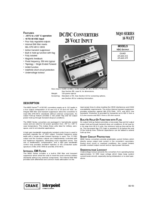
B2-53F EATURES•–55°C to +125°•16 TO 40 VDC input•Four fully regulated outputs •Internal EMI filter meets MIL-STD-461C CE03•Active transient suppressor••Fully isolated•Magnetic feedback•••Inhibit function••Undervoltage lockoutDESCRIPTIONThe MQO Series™of DC/DC converters supply up to 16.5 watts in a four output configuration of ±5 and ±12 or ±5 and ±15 VDC. An integral EMI filter and transient suppressor allow the converters to meet MIL-STD-461C standards without external components. An output hold-up feature provides a low power flag and full output power hold-up through transient dropout conditions.The MQO Series converters are packaged in hermetically sealed cases and are rated for full power operation from –55°to +125°C case temperature. This makes these units ideal for military, aero-space, and hi-rel industrial applications.A high gain bandwidth magnetically isolated control loop is used to precisely regulate the +5 VDC output. Constant frequency pulse width with a single ended forward topology is used. The –5 VDC output and the auxiliary outputs are independently controlled with low headroom regulators, eliminating cross regulation errors. The use of feedforward, compensation, and a high gain bandwidth control loop provides excellent rejection to the conducted audio spectrum of MIL-STD-704A-D and MIL-STD-461C.I NTEGRAL EMI F ILTERThe MQO Series includes a a built-in EMI filter and transient suppressor which allow the units to meet the most common military standards without any external components. The internal EMI filter provides both differential and common mode attenuation on theinput power lines to allow meeting the CE03 interference and CS02 susceptibility requirements. The active internal transient suppressor provides protection against MIL-STD-704A, 1275, and 461C line transients. Protection is provided for transients up to 400 V from a 0.5 ohm source and 600 V from a 50 ohm source.B UILT -I N H OLD -U P F UNCTION WITH F LAGAn output hold-up feature provides a low power flag and full output power hold-up through transient drop out conditions. At full load for a Vin step from 28 to 0 volts, the minimum hold-up time will be 50µs. The low power flag (TTL high) is asserted 10 µs before the end of the hold-up time. External capacitance can be added to extend hold-up time.S HORT C IRCUIT P ROTECTIONMQO Series converters provide predictable current limiters which directly sense output load current in the converter’s secondary.During short circuit or overload conditions, the current limiters provide constant output current and an input power fold-back.U NDERVOLTAGE L OCKOUTUndervoltage lockout prevents the converters from operating below approximately 12 VDC input voltage which helps keep system current levels smooth, especially during initialization or re-start oper-ations.MQO SERIES16 WATTINHIBITTYPICAL CHARACTERISTICSRECOMMENDED OPERATING CONDITIONSABSOLUTE MAXIMUM RATINGSInput Voltage •16 to 40 V Output Power •16.75 wattsLead Soldering Temperature (10 sec per lead)•300°CStorage Temperature Range (Case)•–65°C to +150°CB2-54MQO SERIES 16WATTDC/DC C ONVERTERSUndervoltage Lockout •12 V input typical Isolation•100 megohm minimum at 500 V Audio Rejection •Up to 50 dBConversion Frequency •550 kHz typicalInput Voltage Range•16 to 40 VDC continuousCase Operating Temperature (Tc)•–55°C to +125°C full power •–55°C to +135°C absolute Derating Output Power/Current•Linearly from 100% at 125°C to 0% at 135°CInhibit TTL Open Collector •Logic low (output disabled)•Referenced to input common •Logic high (output enabled)Open collectorMQO28512QMQO28515QPARAMETER CONDITIONMIN TYP MAX MIN TYP MAX UNITSOUTPUT VOLTAGE+5 4.95 5.00 5.05 4.95 5.00 5.05–5 4.95 5.00 5.05 4.95 5.00 5.05+ AUX.11.9012.0012.1014.9015.0015.10VDC– AUX.11.9012.0012.1014.9015.0015.10OUTPUT CURRENT +5390—2000390—2000–50—3500—350+ AUX.0—2080—167mA– AUX.0—2080—167OUTPUT POWER +5 1.95—10.00 1.95—10.00V IN = 16 TO 40 VDC –50— 1.750— 1.75+ AUX.0— 2.500— 2.50W– AUX.0— 2.500— 2.50OUTPUT RIPPLE +5—5055—505510 kHz to 2 MHz –5——30——30+ AUX.——50——50mV p-p– AUX.——50——50LINE REGULATION V IN = 16 TO 36 VDC +5——20——20mV –5, ±AUX.——50——50LOAD REGULATION MINIMUM LOAD TO FULL ±5—20120 —20120 mV±AUX.—50220 —50220INPUT VOLTAGE MINIMUM LOAD TO FULLTc = –55°TO +125°CCONTINUOUS 162840162840VDCTRANSIENT 50ms 0.5 OHM SOURCE ——400——40050 OHM SOURCE ——600——600VINPUT CURRENT MINIMUM LOAD ——230——230FULL LOAD ——960——960mA INHIBITED ——10 —— 10INPUT RIPPLE —50— —50—mA p-p EFFICIENCY 10 kHz TO 2 MHz —64——64—%START-UP DELAY —20——20—msElectrical Characteristics:25°C Tc,28 VDC Vin,100% load,unless otherwise specified.B2-55MQO SERIES16 WATTDC/DC CONVERTERSB2-56MQO SERIES 16 WATTDC/DC C ONVERTERS23624-001-DTS Rev A DQ# 3003All technical information is believed to be accurate, but no responsibility is assumed for errors or omissions. Interpoint reserves the right to make changes in products or specifications without notice. MQO Series is a trademark of Interpoint.Copyright ©1991 - 1999 Interpoint. All rights reserved.CASE N C ASESB8-34C ASESCASE NB8-35TEST (125°C Products)STANDARD/ES/883 (Class H)* PRE-CAP INSPECTIONMethod 2017,2032yes yes yes TEMPERATURE CYCLE (10 times)Method 1010, Cond. C, -65°C to 150°C no no yes Method 1010, Cond. B, -55°C to 125°C no yes no CONSTANT ACCELERATIONMethod 2001, 3000 g no no yes Method 2001, 500 g no yes noBURN-INMethod 1015, 160 hours at 125°C no no yes96 hours at 125°C case (typical)no yes noFINAL ELECTRICAL TEST MIL-PRF-38534, Group ASubgroups 1 through 6: -55°C, +25°C, +125°C no no yes Subgroups 1 and 4: +25°C case yes yes no HERMETICITY TESTINGFine Leak, Method 1014, Cond. A no yes yesGross Leak, Method 1014, Cond. C no yes yesGross Leak, Dip (1 x 10⁻³)yes no noFINAL VISUAL INSPECTIONMethod 2009yes yes yesTest methods are referenced to MIL-STD-883 as determined by MIL-PRF-38534.*883 products are built with element evaluated components and are 100% tested and guaranteed over the full military temperature range of –55°C to +125°C.MOR Series MFLHP Series MFL Series MHP Series MTR Series MQO Series**MHD SeriesMHV SeriesMHF+ SeriesMHF Series**MGA SeriesMSA SeriesMGH SeriesMCH SeriesFM-704A EMI FilterFMD**/FME EMI FilterFMC EMI FilterFMH EMI FilterFMGA EMI FilterFMSA EMI FilterHUM Modules**LCM Modules**LIM ModulesQA SCREENING125°C PRODUCTS125°C P RODUCTSApplies to the following products**MFLHP Series, MQO Series, MHF Series, FMD EMI Filters, Hum Modules, and LCM Modules do not offer ‘883” screening.C2-10。
ISP817中文资料

元器件交易网
ABSOLUTE MAXIMUM RATINGS (25°C unless otherwise specified) Storage Temperature -55°C to + 125°C Operating Temperature -55°C to + 100°C Lead Soldering Temperature (1/16 inch (1.6mm) from case for 10 secs) 260°C INPUT DIODE Forward Current Reverse Voltage Power Dissipation 50mA 6V 70mW
4 3
18 18
Note 1 Note 2
Measured with input leads shorted together and output leads shorted together. Special Selections are available on request. Please consult the factory.
ISP817A,ISP827A,ISP847A ISP817B,ISP827B,ISP847B ISP817C,ISP827C,ISP847C ISP817D,ISP827D,ISP847D
100
Coupled
ISP817GB, ISP827GB, ISP847GB ISP817BL, ISP827BL, ISP847BL
35V 6V 150mW
200mW
ELECTRICAL CHARACTERISTICS ( TA = 25°C Unless otherwise noted ) PARAMETER Input Forward Voltage (VF) Reverse Voltage (VR) Reverse Current (IR) MIN TYP MAX UNITS 1.2 6 10 1.4 V V µA V V nA TEST CONDITION IF = 20mA IR = 10µA VR = 6V IC = 1mA IE = 100µA VCE = 20V 5mA IF , 5V VCE 5mA IF , 5V VCE 5mA IF , 5V VCE 5mA IF , 5V VCE 5mA IF , 5V VCE 5mA IF , 5V VCE 5mA IF , 5VVCE 20mA IF , 1mA IC See note 1 See note 1 VIO = 500V (note 1) VCE = 2V , IC = 2mA, RL = 100Ω
(参考资料)SJ-D主轴参数

12 0 0 0 0 0 0 0 0 0 0 0 2
22 120
0 10000
1500 1800 1262
73 3252 2427 1947
145 0 0 0
Name SP145 SP146 SP147 SP148 SP149 SP150 SP151 SP152 SP153 SP154 SP155 SP156 SP157 SP158 SP159 SP160 SP161 SP162 SP163 SP164 SP165 SP166 SP167 SP168 SP169 SP170 SP171 SP172 SP173 SP174 SP175 SP176 SP177 SP178 SP179 SP180 SP181 SP182 SP183 SP184 SP185 SP186 SP187 SP188 SP189 SP190 SP191 SP192
Set1 15 33 15 0 150
1900 0
150 1900
0 0 0 0 50 100 20 000C 0000 2000 2000 60 120 120 875 875 10000 25 1000 30 0 2200 0019 0000 0000 1600 0000 100 0 0 0 0 0 0 0 0 0 100 0
[Set1] Drive unit
:MDS-D-SP-160
[Set2] Drive unit
:MDS-D-SPJ3-75
Power supply unit:MDS-D-CV-□
Power supply unit:FCUA-RB□/R-UNIT□
Motor
:SJ-D7.5/100-01+MBE205(2000kp/rev)
- 1、下载文档前请自行甄别文档内容的完整性,平台不提供额外的编辑、内容补充、找答案等附加服务。
- 2、"仅部分预览"的文档,不可在线预览部分如存在完整性等问题,可反馈申请退款(可完整预览的文档不适用该条件!)。
- 3、如文档侵犯您的权益,请联系客服反馈,我们会尽快为您处理(人工客服工作时间:9:00-18:30)。
元器件交易网
MKT 1817
Vishay Roederstein
CAPACITANCE CAPACITANCE CODE
Metallized Polyester, Related Document: IEC 60384-2
VOLTAGE CODE 06 63 VDC/ 40 VAC W H — — — — — — — — — — — — 6.0 8.5 8.5 9.5 10.0 10.5 11.5 L — — — — — — — — — — — — 7.5 7.5 7.5 7.5 7.5 7.5 7.5 W — — — — — — — — 2.5 2.5 2.5 2.5 3.5 4.5 5.0 5.5 — — — VOLTAGE CODE 01 100 VDC/ 63 VAC H — — — — — — — — 6.0 6.0 6.0 6.0 8.5 9.5 10.0 11.5 — — — L — — — — — — — — 7.5 7.5 7.5 7.5 7.5 7.5 7.5 7.5 — — — W — — — 2.5 2.5 2.5 2.5 2.5 3.0 3.5 4.5 4.5 5.5 — — — — — — VOLTAGE CODE 25 250 VDC/ 160 VAC H — — — 6.0 6.0 6.0 6.0 6.0 6.5 8.5 9.5 9.5 11.5 — — — — — — L — — — 7.5 7.5 7.5 7.5 7.5 7.5 7.5 7.5 7.5 7.5 — — — — — — W 2.5 2.5 2.5 3.0 3.5 3.5 4.5 5.0 5.5 — — — — — — — — — — VOLTAGE CODE 40 400 VDC/ 200 VAC H 6.0 6.0 6.0 6.5 8.5 8.5 9.5 10.0 11.5 — — — — — — — — — — L 7.5 7.5 7.5 7.5 7.5 7.5 7.5 7.5 7.5 — — — — — — — — — —
0.1 0.2 2
0.4 7
Vishay Roederstein
0.0
Capacitance in µF
102 7 5 3 2 101 7 5 3 2 100 VDC 100 102 2 3 5 7 103 2 3
Capacitance in µF
22 0.0 47 0.1 5 0.3 3
1.0
5 7 104
1000 pF 1500 pF 2200 pF 3300 pF 4700 pF 6800 pF 0.01 µF 0.015 µF 0.022 µF 0.033 µF 0.047 µF 0.068 µF 0.1 µF 0.15 µF 0.22 µF 0.33 µF 0.47 µF 0.68 µF 1.0 µF
1250 s minimum value (10,000 s typical value)
IEC TEST CLASSIFICATION:
55/100/56, according to IEC 60068
CAPACITANCE DRIFT:
Up to + 40°C, ± 1.5% for a period of two years
1.6 x UR for 2 s
RELIABILITY:
Operational life > 300,000h Failure rate < 2 FIT (40°C and 0.5 x UR) For further details, please refer to the general information provided in this catalog.
2 3
5 7 105 f [Hz]
Permissible AC Voltage versus Frequency
Permissible AC Voltage versus Frequency
V RMS
V RMS
103 7 5 3 2 10 7 5 3 2 101 250 VDC 102 2 3 5 7 103 2 3
OPERATING TEMPERATURE RANGE:
- 55°C to + 100°C
CAPACITANCE RANGE:
1000pF to 1.0µF
DERATING FOR DC AND AC. CATEGORY VOLTAGE UC:
At + 85°C: UC = 1.0 UR At + 100°C: UC = 0.8 UR
元器件交易网
MKT 1817
Metallized Polyester, Related Document: IEC 60384-2
V RMS V RMS
102 7 5 3 2 101 7 5 3 2 100 63 VDC 102 2 3 5 7 103 2 3 5 7 104 2 3 5 7 105 f [Hz]
INSULATION RESISTANCE:
Measured with 100 VDC (63 VDC series measured at 50 VDC) after one minute
For C ≤ 0.33µF and UR > 100 VDC: For C ≤ 0.33µF and UR ≤ 100 VDC: MAXIMUM PULSE RISE TIME
Document Number 26032 Revision 01-Dec-03 For technical questions, contact dc-film@ 37
-3
0.1µF < C ≤ 1.0µF 8 x 10⁻³ 15 x 10-3 —
CONSTRUCTION:
Extended metallized film (refer to general information)
TIME CONSTANT:
Measured with 50 VDC after one minute
LEADS:
Tinned wire
For C > 0.33µF:
CAPACITANCE TOLERANCES:
± 20% (M), ± 10% (K), ± 5% (J)
SELF INDUCTANCE:
~ 6nH measured with 2mm long leads
RATED VOLTAGES (UR):
63 VDC, 100 VDC, 250 VDC, 400 VDC
7500 MΩ minimum value (100,000 MΩ typical value) 3750 MΩ minimum value (50,000 MΩ typical value)
Maximum pulse rise time dv/dt [V/µs]
PCM (mm) 5 63 VDC 15 100 VDC 24 250 VDC 44 400 VDC 100
元器件交易网
MKT 1817
Vishay Roederstein
Metallized Polyester Film Capacitors Related Document: IEC 60384-2
MAIN APPLICATIONS:
Blocking, bypassing, filtering and timing, high frequency coupling and decoupling for fast digital and analog ICs, interference suppression in low voltage applications.
If the maximum pulse voltage is less than the rated voltage higher dv/dt values can be permitted.
DISSIPATION FACTOR TAN δ
MEASURED AT 1kHz 10kHz 100kHz C ≤ 0.1µF 8 x 10 15 x 10-3 25 x 10-3 Maximum values
- 210 - 215 - 222 - 233 - 247 - 268 - 310 - 315 - 322 - 333 - 347 - 368 - 410 - 415 - 422 - 433 - 447 -468 - 510
— — — — — — — — — — — — 2.5 3.5 3.5 4.5 5.0 5.0 5.5
PULL TEST ON LEADS:
≥ 30 N in direction of leads according to IEC 60068-2-21
PERMISSIBLE AC VOLTAGES (RMS) UP TO 60Hz:
40 VAC, 63 VAC, 160 VAC, 200 VAC
TEST VOLTAGE (ELECTRODE/ELECTRODE):
L Max. H Max.
Dimensions in millimeters
W Max. Marking
MARKING:
Manufacturer's logo/type/C-value/rated voltage/tolerance/ date of manufacture
0.6
DIELECTRIC:
*S = box size 55 x 210 x 340mm (W x H x L)
38
For technical questions, contact dc-film@
Document Number 26032 Revision 01-Dec-03
Polyester film
6.0-1