BL8505-303RM中文资料
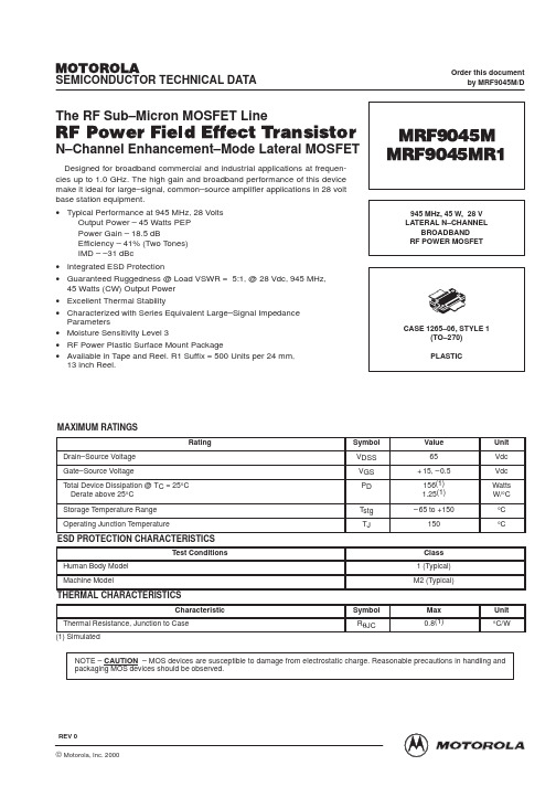
MRF9045M中文资料
Z3 Z4 Z5 Z6 Z7 Z8 Z9 Z10 Z11 Z12 Z13
0.14″ x 0.32″ 0.47″ x 0.32″ 0.16″ x 0.32″ x 0.62″ Tapered 0.18″ x 0.62″ 0.56″ x 0.62″ 0.33″ x 0.32″ 0.14″ x 0.32″ 0.36″ x 0.08″ 1.01″ x 0.08″ 0.15″ x 0.08″ 0.29″ x 0.08″
N–Channel Enhancement–Mode Lateral MOSFET
MRF9045M MRF9045MR1
945 MHz, 45 W, 28 V LATERAL N–CHANNEL BROADBAND RF POWER MOSFET
CASE 1265–06, STYLE 1 (TO–270) PLASTIC
mrf9045m中文资料lm358中文资料12864中文资料lm393中文资料mpu6050中文资料lm324中文资料7805中文资料max232中文资料tl431中文资料op07中文资料74hc595中文资料
元器件交易网
MOTOROLA
SEMICONDUCTOR TECHNICAL DATA
MAXIMUM RATINGS
Rating Drain–Source Voltage Gate–Source Voltage Total Device Dissipation @ TC = 25°C Derate above 25°C Storage Temperature Range Operating Junction Temperature Symbol VDSS VGS PD Tstg TJ Value 65 + 15, – 0.5 156(1) 1.25(1) – 65 to +150 150 Unit Vdc Vdc Watts W/°C °C °C
BL8505 Datasheet(中文资料)
BL8505 Datasheet(中文资料)BL8505概述:BL8505 系列是PFM 控制的开关型DC/DC 升压稳压芯片。
0.8V 的启动电压、高达180mA 的负载驱动能力(当Vin=1.5V,Vout=3.3V)、87%的转换效率(Vin>2V,Vout=3.3V,Iout<100mA)使得BL8505 非常适合于便携式1~4 节普通电池应用的场合。
BL8505 在电路设计及生产中,特别针对开关电路固有的噪声问题进行了改良,极大的减小了对其周边电路的干扰。
BL8505 电路采用了高性能的参考电压电路结构,以及在生产中引入修正技术,保证了输出电压的高输出精度及低温度漂移。
BL8505 可提供SOT-89-3、TO-92 及SOT-23-5 等封装形式。
在SOT-23-5 等封装形式中,通过CE 使能端,可方便控制芯片的开关,使芯片的功耗达到最小。
BL8505特点:• 极强负载驱动能力:Vin=1V 时可提供3.3V、50mA 的负载电流,Vin=1.5V 时可提供3.3V、180mA 的负载电流• 0.8V 极低的启动电压(Iout=1mA 时)• 2.5V~5.0V 输出电压范围(0.1V 步进,可根据客户需求进行定制)• 输出电压精度可达±2%• 低输出电压温度漂移:±100ppm/℃• 仅需电感、电容、肖特基二极管三个外部元件• 效率高达87%• SOT89-3,TO-92,SOT-23-5 多种封装形式BL8505用途:• PDA、DSC、MP3 Player、电动玩具、无线鼠标等便携式电池供电设备• 单、双节电池供电设备的电源部分• 给LED 灯提供能源。
BL8506-30NRM中文资料
TPLH
Parameter Detector Threshold Detector Threshold
Hysteresis Current consumption Maximum operating
voltage Minimum Operating
voltage
Output current
Output Delay Time
Selection Guide: BL8506-XX X XX
Pin Assignment:
Package Type: RM: SOT-23-3 RN: SOT-23-5 SM: SOT-89-3 T: TO-92 (Default、Pb Free)
Output Type: N:Nch Open-drain C:CMOS
voltage Minimum Operating
voltage
Output current
Output Delay Time
Conditions
VDD=4.7V
Nch VDS=0.05V, VDD=0.70V Pch VDS=-2.1V, VDD=4.50V
Reference data
Min.
Typ.
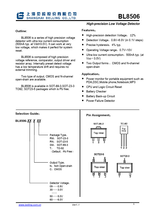
BL8506 is composed of high precision voltage reference, comparator, output driver and resistor array. Internally preset detect voltage has a low temperature drift and requires no external trimming.
Two type of output, CMOS and N-channel open-drain are available.
SUP57N20-33_08中文资料
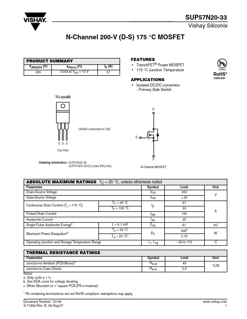
Vishay SiliconixSUP57N20-33N-Channel 200-V (D-S) 175 °C MOSFETFEATURES•TrenchFET ® Power MOSFET •175 °C Junction TemperatureAPPLICATIONS•Isolated DC/DC converters- Primary-Side SwitchPRODUCT SUMMARYV(BR)DSS (V)r DS(on) (Ω)I D (A)2000.033 at V GS = 10 V57Notes:a. Duty cycle ≤ 1 %.b. See SOA curve for voltage derating.c. When Mounted on 1" square PCB (FR-4 material).* Pb containing terminations are not RoHS compliant, exemptions may apply.ABSOLUTE MAXIMUM RATINGS T C = 25°C, unless otherwise notedParameterSymbol Limit Unit Drain-Source Voltage V DS 200VGate-Source VoltageV GS± 20Continuous Drain Current (T J = 175 °C)T C = 25 °C I D 57AT C = 125 °C33Pulsed Drain Current I DM 140Avalanche CurrentI AS35Single Pulse Avalanche Energy a L = 0.1 mH E AS 61mJ Maximum Power DissipationaT C = 25 °C P D 300b W T A = 25 °C c3.75Operating Junction and Storage T emperature RangeT J , T stg- 55 to 175°CTHERMAL RESISTANCE RATINGSParameterSymbol Limit Unit Junction-to-Ambient (PCB Mount)c R thJA 40°C/WJunction-to-Case (Drain)R thJC0.5Vishay SiliconixSUP57N20-33Notes:a. Pulse test; pulse width ≤ 300 µs, duty cycle ≤ 2 %.b. Guaranteed by design, not subject to production testing.c. Independent of operating temperature.Stresses beyond those listed under “Absolute Maximum Ratings” may cause permanent damage to the device. These are stress ratings only, and functional operation of the device at these or any other conditions beyond those indicated in the operational sections of the specifications is not implied. Exposure to absolute maximum rating conditions for extended periods may affect device reliability.SPECIFICATIONS T J = 25°C, unless otherwise notedParameter Symbol Test Conditions Min Typ Max UnitStaticDrain-Source Breakdown Voltage V (BR)DSS V DS = 0 V , I D = 250 µA 200V Gate-Threshold Voltage V GS(th) V DS = V GS , I D = 250 µA 24Gate-Body LeakageI GSS V DS = 0 V, V GS = ± 20 V ± 100nAZero Gate Voltage Drain Current I DSS V DS = 160 V , V GS = 0 V 1µA V DS = 160 V, V GS = 0 V , T J = 125 °C 50V DS = 160 V, V GS = 0 V , T J = 175 °C250On-State Drain Current aI D(on) V DS ≥ 5 V , V GS = 10 V 120A Drain-Source On-State Resistance a r DS(on) V GS = 10 V, I D = 30 A 0.0270.033ΩV GS = 10 V, I D = 30 A, T J = 125 °C 0.069V GS = 10 V, I D = 30 A, T J = 175 °C0.093Forward T ransconductance a g fsV DS = 15 V , I D = 30 A25S Dynamic bInput Capacitance C iss V GS = 0 V , V DS = 25 V , f = 1 MHz5100pFOutput CapacitanceC oss 480Reverse Transfer Capacitance C rss 210Total Gate Charge c Q g V DS = 100 V , V GS = 10 V , ID = 85 A 90130nC Gate-Source Charge c Q gs 23Gate-Drain Charge c Q gd 34Turn-On Delay Time c t d(on) V DD = 100 V, R L = 1.5 Ω I D ≅ 65 A, V GEN = 10 V , R G = 2.5 Ω2435nsRise Time ct r 220330Turn-Off Delay Time c t d(off) 4570Fall Time ct f200300Source-Drain Diode Ratings and Characteristics (T C = 25°C)b Continuous Current I S 65A Pulsed Current I SM 140Forward Voltage a V SD I F = 65 A, V GS = 0 V 1.0 1.5V Reverse Recovery Time t rr I F = 50 A, di/dt = 100 A/µs130200ns Peak Reverse Recovery Current I RM(REC)812A Reverse Recovery ChargeQ rr0.521.2µCOutput CharacteristicsTransfer CharacteristicsVishay SiliconixSUP57N20-33TYPICAL CHARACTERISTICS 25°C, unless otherwise notedAvalanche Current vs. TimeDrain Source Breakdown vs. Junction TemperatureVishay SiliconixSUP57N20-33THERMAL RATINGSVishay Silicon ix main tain s worldwide man ufacturin g capability. Products may be man ufactured at on e of several qualified location s. Reliability data for Silicon Technology and Package Reliability represent a composite of all qualified locations. For related documents such as package/tape drawin gs, part markin g, an d reliability data, see /ppg?72100.Maximum Avalanche and Drain Currentvs. Case TemperatureSafe Operating AreaNormalized Thermal Transient Impedance, Junction-to-CaseDisclaimer Legal Disclaimer NoticeVishayAll product specifications and data are subject to change without notice.Vishay Intertechnology, Inc., its affiliates, agents, and employees, and all persons acting on its or their behalf (collectively, “Vishay”), disclaim any and all liability for any errors, inaccuracies or incompleteness contained herein or in any other disclosure relating to any product.Vishay disclaims any and all liability arising out of the use or application of any product described herein or of any information provided herein to the maximum extent permitted by law. The product specifications do not expand or otherwise modify Vishay’s terms and conditions of purchase, including but not limited to the warranty expressed therein, which apply to these products.No license, express or implied, by estoppel or otherwise, to any intellectual property rights is granted by this document or by any conduct of Vishay.The products shown herein are not designed for use in medical, life-saving, or life-sustaining applications unless otherwise expressly indicated. Customers using or selling Vishay products not expressly indicated for use in such applications do so entirely at their own risk and agree to fully indemnify Vishay for any damages arising or resulting from such use or sale. Please contact authorized Vishay personnel to obtain written terms and conditions regarding products designed for such applications.Product names and markings noted herein may be trademarks of their respective owners.元器件交易网。
AA51880中文资料
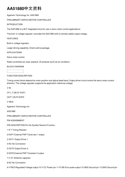
AA51880中⽂资料Agamem Technology Inc. AA51880PRELIMINARY SERVO MOTOR CONTROLLERINTRODUCTIONThe AA51880 is a BJT integrated circuit for use in servo motor control applications.The built -in voltage regulato r provides the AA51880 with ex tremely stable output voltage.FEATURESBuilt-in voltage regulator.Larger driving capability. Small outline package.APPLICATIONSServo motor control.Radio controlled car, boat, airplane. IA products (such as air-condition).BLOCK DIAGRAMFUNCTION DESCRIPTIONTiming control block detects the motor position and adjust dead band. Output driver circuit control the servo motor current direction. The voltage regulator supports the application reference voltage.V INOT L T DB ST EXP1OUT1 OUT2 EXP2V REGAgamem Technology Inc.AA51880PRELIMINARY SERVO MOTOR CONTROLLERPIN ASSIGNMENTPIN DESCRIPTION Pin No Symbol Name & Function1 R T Timing Resistor2 EXP1 External PNP Transi stor 1 output3 OUT1 Output Driver 14 NC No Connection5 OUT2 Output Driver 26 EXP2 External PNP Transistor 2 output7 C ST Stretcher capacitor8 NC No Connection9 V REG Regulated Voltage output 10 V CC Power pin 11 R DB Error pulse output 12 GND Ground pin 13 GND Ground pin14 V IN Input signal15 P OT Servo position voltage 16C TTiming Capacitor12345678161514131211109(Top View)R T EXP1OUT1NC OUT2EXP2C ST NCC T P OT V IN GND GND R DB Vcc V REGAA51880Agamem Technology Inc.AA51880PRELIMINARY SERVO MOTOR CONTROLLERRATINGS (Ta=25¢J, unless otherwise noted)ELECTRICAL CHARACTERISTICS (Ta=25¢J and Vcc=4.8V, unless otherwise noted)VOLTAGE REGULATOR OUTPUT VOLTAGE CHARACTERISTIC (Ta=25¢J)4321V CC V R e gAgamem Technology Inc.AA51880 PRELIMINARY SERVO MOTOR CONTROLLER APPLICATION CIRCUITAgamem Technology Inc.AA51880PRELIMINARYSERVO MOTOR CONTROLLERn SSOP PACKAGE DIMENSIONPLAN。
RM009中文资料
GSM VBSLMAX
—
DCS VBSHMIN
—
0.5
V
2.0
V
2
Skyworks Solutions, Inc. Proprietary
101258B
July 26, 2002
元器件交易网
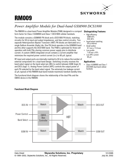
RM009
Power Amplifier Module for Dual-band GSM900 DCS1800 Applications
RF input and output ports are internally matched to 50 Ω to reduce the number of external components for a dual-band design. Switching circuitry receives the band select signal on the band select pin (BS) to switch between GSM (logic 0) and DCS (logic 1). Analog Power Control (APC) controls the output power of each PA selected by the band select signal. The extremely low leakage current (2 µA, typical) of the RM009 dual-band module maximizes handset standby time.
Electrical Specifications
Table 1 provides the absolute maximum ratings of the RM009, Table 2 shows the recommended operating conditions and Table 3 shows the electrical characteristics.
ATV303
Modbus 与 CANopen
Modbus TCP,Fipio,Modbus/UniTelway,Modbus Plus,EtherNet/IP, DeviceNet,PROFIBUS DP,PROFIBUS DP V1,INTERBUS S,CC-Link
I/O扩展卡,“Controller Inside” (内置控制器) 可编程卡,多泵卡
0.5...400 Hz
0.37...11 – – – – – 0.37...11 – –
0.5...400 Hz
0.18...15 – 0.18...2.2 – 0.18...15 – 0.37...15 0.75...15 –
0.5...500 Hz
标准 (电压/频率比) 高性能 (无传感器磁通矢量控制) 风机/泵 (Kn2二次比)
ATV 12
请参考“ATV12 变频器” 产品目录
IEC/EN 61800-5-1,
IEC/EN 61800-3 (环境1与2,C1至C3类)
IEC/EN 61800-5-1,
IEC/EN 61800-3 (环境1与2,C1至C3类) e,UL,CSA,C-Tick, NOM,GOST
ATV 303
• 集成标准 Modbus 通讯协议,能够方便地与其他设备进行通讯 • 冷却风量异常报警功能,方便维护,尤其适合纺机行业
施耐德全新自动化平台
HMI STU/STO
STO/STU触摸屏、M218 PLC和 ATV303 变频 器是施耐德电气推出的全新自动化平台。 产品性价比高,更适合中国市场需求。
节省您的支出
1
选型指南
机械类型
异步与同步电机变频器
简单机械
对于 50...60 Hz (kW)电源的功率范围 单相 100...120 V (kW) 单相 200...240 V (kW)
BL8505中文资料

450
500
Output Current(mA)
Ver1.1
7/10
元器件交易网
BL8505
L=10uH
100
(%)
90 80 70 60 50 0 50 100 150 200 250 300 350 400 Vin=0.9V Vin=1.0V Vin=1.5V Vin=1.8V Vin=2.0V 450 500
Function description
Output voltage
Ver1.1
Pin Description:
Pin No.
SOT-89-3 TO-92 SOT-23-3 SOT-89-5 SOT-23-5
Vout Vin Vout
Ver1.1
4/10
元器件交易网
BL8505
L min D(1 D) RL 2f
2
Lmin
D Vin Lf Vin Im ax (1 D) 2 RL I
DVin 2 Lf
rL Rload (1 D) 2
2
Capacitor Selection
Output Current(mA)
L=47uH
140
Ripple Voltage Vr(mVp-p)
120 100 80 60 40 20 0 0 50 100 150 200 250 300 350 400 Vin=0.9V Vin=1.0V Vin=1.5V Vin=1.8V Vin=2.0V 450 500
r
Vout Vout
D Rload Cf
r' r
Im ax RESR Vout
3
Diode Selection
- 1、下载文档前请自行甄别文档内容的完整性,平台不提供额外的编辑、内容补充、找答案等附加服务。
- 2、"仅部分预览"的文档,不可在线预览部分如存在完整性等问题,可反馈申请退款(可完整预览的文档不适用该条件!)。
- 3、如文档侵犯您的权益,请联系客服反馈,我们会尽快为您处理(人工客服工作时间:9:00-18:30)。
Vout Vin Vout
Ver1.1
4/10
元器件交易网
BL8505
L min D(1 D) RL 2f
2
Lmin
D Vin Lf Vin Im ax (1 D) 2 RL I
DVin 2 Lf
rL Rload (1 D) 2
2
Capacitor Selection
r
Vout Vout
D Rload Cf
r' r
Im ax RESR Vout
3
Diode Selection
Ver1.1
5/10
元器件交易网
BL8505
4 Input Capacitor
Test Circuits
3
Output Current(mA)
Ver1.1
8/10
元器件交易网
BL8505
L=100uH
3.3 3.2 3.1 3 2.9 2.8 2.7 0 50 100 150 200 250 300 350 400
Output Voltage(V)
Output Current(mA)
L=47uH
140
Ripple Voltage Vr(mVp-p)
120 100 80 60 40 20 0 0 50 100 150 200 250 300 350 400 Vin=0.9V Vin=1.0V Vin=1.5V Vin=1.8V Vin=2.0V 450 500
2/10
元器件交易网
BL8505
Recommended Operating Conditions:
Min Nom Max Unit
*Suggestion
Electrical Characteristics:
Symbol Item Test Conditions Min Reference Data Typ. Max Unit
Efficiency
Output Current(mA)
L=47uH
3.5 3.4
Output Voltage(V)
3.3 3.2 3.1 3 2.9 2.8 2.7 0 50 100 150 200 250 300 350 400
Vin=0.9V Vin=1.0V Vin=1.5V Vin=1.8V Vin=2.0V
Ver1.1
6/10
元器件交易网
BL8505
Typical Characteristics
L=10uH
3.5 3.4
Vin=0.9V Vin=1.0V Vin=1.5V Vin=1.8V Vin=2.0V
Output Voltage(V)
3.3 3.2 3.1 3 2.9 2.8 2.7 0 50 100 150 200 250 300 350 400
Symbol
Description
Product List:
Product Name Output Voltage LX Tr. Driver Chip Enable Package
Block Diagram
Absolute Maximum Ratings:
Ver1.1
Ver1.1
3/10
元器件交易网
BL8505
Typical Characteristics
Detailed Description:
Selection Of The External Components:
D
1 Inductor Selection
Output Current(mA)
Ver1.1
9/10
元器件交易网
BL8505
Package Outline
Ver1.1
10/10
450
500
Output Current(mA)
L=47uH
100
(%) Efficiency
90 80
Vin=0.9V
70 60 50 0 50 100 150 200 250 300 350 400
Vin=1.0V Vin=1.5V Vin=1.8V Vin=2.0V Vin=2.5V
450
500
Vin=0.9V Vin=1.0V Vin=1.5V Vin=1.8V Vin=2.0V
450
500
Output Current(mA
Vin=0.9V Vin=1.0V Vin=1.5V Vin=1.8V Vin=2.0V
(%)
70 60 50 0 50 100 150 200 250 300 350 400 450 500
Function description
Output voltage
Ver1.1
1/10
元器件交易网
BL8505
Pin Description:
Pin No.
SOT-89-3 TO-92 SOT-23-3 SOT-89-5 SOT-23-5
元器件交易网
BL8505
High Efficiency PFM Step-up DC/DC Converter Outline Features
Applications
Selection Guide
BL8505 XX X XX
package
Pin Configurations
450
500
Output Current(mA)
Ver1.1
7/10
元器件交易网
BL8505
L=10uH
100
(%)
90 80 70 60 50 0 50 100 150 200 250 300 350 400 Vin=0.9V Vin=1.0V Vin=1.5V Vin=1.8V Vin=2.0V 450 500