C8051Fxx单片机开发工具及调试技术
操作指南
U-EC5操作指南简介C8051F单片机的低价位开发套件是为您提供快速开发应用系统的工具。
该套件包含了开发所需的软件和硬件,性能优于传统的仿真器。
U-EC5具有:完全的USB2.0接口、免安装驱动程序、硬件加强型保护功能(减少使用不当造成的硬件损坏率)。
该工具可实现单步、连续单步、断点、停止/运行,支持寄存器/存储器的观察和修改,下载程序到Flash存储器等功能。
另一特点为可使用专用软件(U-EC5中文编程软件)快速将程序代码烧录到C8051F MCU中。
一、U-EC5调试适配器操作说明1. 说明: 1.1 U-EC5调试适配器适用于C8051FXXX系列的所有芯片。
1.2 软件运行环境:Microsoft Winodows 98/2000/NT/XP。
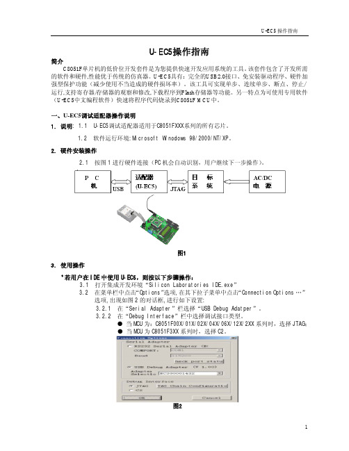
2. 硬件安装操作2.1 按图1进行硬件连接(PC机会自动识别,用户继续下一步操作)。
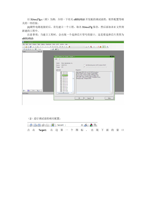
图13. 使用操作*若用户在IDE中使用U-EC5,则按以下步骤操作:3.1 打开集成开发环境“Silicon Laboratories IDE.exe”3.2 在菜单栏中点击“Options”选项,在其下拉子菜单中点击“Connection Options …”选项,出现如图2的对话框,进行如下设置:3.2.1 在“Serial Adapter”栏选择“USB Debug Adatper”。
3.2.2 在“Debug Interface”栏中选择调试接口类型。
●当MCU为:C8051F00X/01X/02X/04X/06X/12X/2XX系列时,选择JTAG;●当MCU为C8051F3XX系列时,选择C2。
图24、在菜单栏中点击“Debug”选项,在其下拉子菜单中点击“Connect”选项,进行连接。
成功则会激活“Debug”菜单下的其它操作,如图3。
图35、点击工程栏中的“New Project”选项,再点击鼠标右键,在出现的对话框中点击“Save ProjectNew_Project”选项,在出现的“Save Workspace”对话框中为要建的工程起个新名并保存起来,工程栏中会出现新的工程名,例新的工程名为Project1,如图4。
C8051F单片机常见问题及解决方案

C8051F单片机常见问题及解决方案1000字C8051F单片机常见问题及解决方案C8051F系列单片机是一款常用的32位微型控制器。
在使用中,常常会遇到各种问题,以下列出了一些常见问题及解决方案,供大家参考。
1.如何选择晶振?C8051F单片机的内部时钟频率有两种选择:内部振荡器(24MHz)和外部晶振(最高可达25MHz,具体要看选用的晶振规格)。
选择晶振时,可以考虑系统时钟的需求量,以及对系统稳定性的要求。
2.如何处理硬件复位?硬件复位是指在单片机系统上电时,自动执行初始化操作的过程。
C8051F单片机实现硬件复位的方法有两种:使用复位电路(RST#复位)、通过预编程的复位向量(从C2寄存器获取程序计数器初始值)。
通常情况下,我们可以使用预编程的复位向量,以方便地重新启动程序。
3.如何处理软件复位?软件复位是指通过程序代码实现的复位。
在C8051F单片机中,软件复位可以通过配置系统管理单元(SMU)来实现。
这个过程通常包括设置复位源、配置访问时间窗口、启用复位源、复位等操作。
在进行软件复位之前,我们需要仔细查看数据手册中的相关章节,并根据实际需求进行配置。
4.如何配置GPIO口?GPIO(通用输入输出)口是单片机系统中的基本输入输出接口,用于实现I/O操作和外设控制等功能。
在C8051F单片机中,GPIO口的配置可以通过专用寄存器(P0、P1、P2、P3等)来实现。
具体的配置包括:指定口线方向、设置上下拉电阻、确定端口中断引脚等。
5.如何编写中断服务程序?中断服务程序是用于响应中断请求、处理相应事件的程序代码实现。
在C8051F单片机中,编写中断服务程序包括两个步骤,一是将中断请求源打开(或禁止),二是编写相应的中断处理程序。
具体的实现方法会有一些细微的差别,需要仔细查看数据手册中的相关章节。
6.如何使用定时器?定时器是单片机中常用的计时器件,用于实现时间处理、调度和控制等功能。
在C8051F单片机中,使用定时器需要涉及一些内容,包括:设置定时器的工作模式、配置计数器时钟源和初始化计数器等。
C8051F310开发板调试
以31kou27g.c(附)为例,介绍一下有关c8051f310开发板的调试流程,软件配置等相关的一些经验。
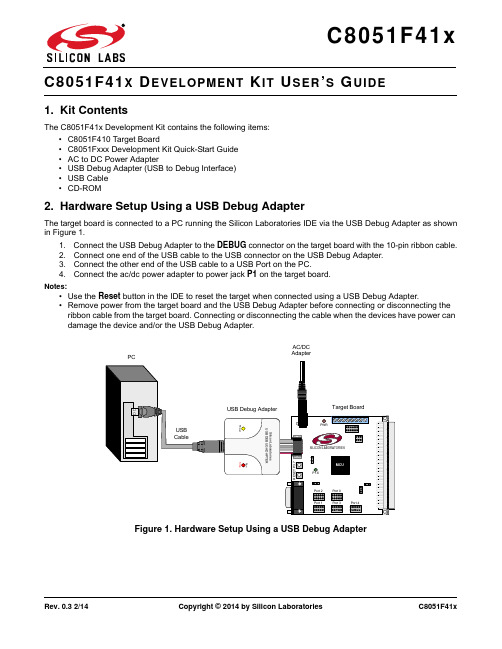
(1)硬件电路连接好后,首先建立一个工程,取名31kou27g保存,然后添加该C文件到新建的工程中。
注意事项:当建立工程时,会出现一个选择芯片型号的窗口,这是要选择芯片类型为c8051f310:(2)进行调试前的相关配置:点击Target1右边第一个图标,出现下面的窗口第一项Device因为前面已经选好了,就不用再管了。
点击Output将打勾选中。
下面点击Debug:这里我们因为连接了硬件,所以选择,注意下拉列表中选择C8051Fxxx Driver。
并且在右边的Setting中选择(3)所有这些配置好以后,点OK,进行DEBUG调试,出现下面的界面,点击单步运行,或者按F10(F11),随着不断运行,可以看到两个小灯不断亮灭。
点击全速运行,然后可以看到小灯自己不断闪烁。
另外点解Load可以将Hex文件烧写进芯片,就不用其他烧写工具了,很方便。
如果直接下载,不经过DEBUG,还需要进行一些设置:选择最右边的这个选项,如下载设置附:keil4的安装破解(1)首先,下载keil4安装(2)打开出现如下界面需要填写CID号,打开keil4,选择License Management将CID号复制,粘贴到上面,点击generate,将产生的序列号复制到New License ID Code,点击Add LIC,设置好以后点击Close.这样就设置好了,可以放心使用。
另外还有很重要的一个步骤,就是安装调试器驱动驱动安装位置要选择在keil软件的安装位置下!正确安装软件及驱动后,就可找到的。
C8051F41x开发套件用户指南说明书
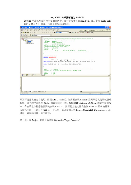
Rev. 0.3 2/14Copyright © 2014 by Silicon LaboratoriesC8051F41xX EVELOPMENT IT SER S UIDE1. Kit ContentsThe C8051F41x Development Kit contains the following items:•C8051F410 Target Board•C8051Fxxx Development Kit Quick-Start Guide •AC to DC Power Adapter•USB Debug Adapter (USB to Debug Interface)•USB Cable •CD-ROM2. Hardware Setup Using a USB Debug AdapterThe target board is connected to a PC running the Silicon Laboratories IDE via the USB Debug Adapter as shown in Figure 1.1.Connect the USB Debug Adapter to the DEBUG connector on the target board with the 10-pin ribbon cable.2.Connect one end of the USB cable to the USB connector on the USB Debug Adapter.3.Connect the other end of the USB cable to a USB Port on the PC.4.Connect the ac/dc power adapter to power jack P1 on the target board.Notes:•Use the Reset button in the IDE to reset the target when connected using a USB Debug Adapter.•Remove power from the target board and the USB Debug Adapter before connecting or disconnecting the ribbon cable from the target board. Connecting or disconnecting the cable when the devices have power can damage the device and/or the USB Debug Adapter.Figure 1.Hardware Setup Using a USB Debug AdapterPWRP1.6C8051F41x3. Software SetupSimplicity Studio greatly reduces development time and complexity with Silicon Labs EFM32 and 8051 MCU products by providing a high-powered IDE, tools for hardware configuration, and links to helpful resources, all in one place.Once Simplicity Studio is installed, the application itself can be used to install additional software and documentation components to aid in the development and evaluation process.Figure2.Simplicity StudioThe following Simplicity Studio components are required for the C8051F410 Development Kit:⏹ 8051 Products Part Support ⏹ Simplicity Developer PlatformDownload and install Simplicity Studio from /8bit-software or /simplicity-studio .Once installed, run Simplicity Studio by selecting Start →Silicon Labs →Simplicity Studio →Simplicity Studio from the start menu or clicking the Simplicity Studio shortcut on the desktop. Follow the instructions to install the software and click Simplicity IDE to launch the IDE.The first time the project creation wizard runs, the Setup Environment wizard will guide the user through the process of configuring the build tools and SDK selection.In the Part Selection step of the wizard, select from the list of installed parts only the parts to use during development. Choosing parts and families in this step affects the displayed or filtered parts in the later device selection menus. Choose the C8051F41x family by checking the C8051F41x check box. Modify the part selection at any time by accessing the Part Management dialog from the Window →Preferences →Simplicity Studio →Part Management menu item.Simplicity Studio can detect if certain toolchains are not activated. If the Licensing Helper is displayed after completing the Setup Environment wizard, follow the instructions to activate the toolchain.C8051F41x3.1. Running BlinkyEach project has its own source files, target configuration, SDK configuration, and build configurations such as the Debug and Release build configurations. The IDE can be used to manage multiple projects in a collection called a workspace. Workspace settings are applied globally to all projects within the workspace. This can include settings such as key bindings, window preferences, and code style and formatting options. Project actions, such as build and debug are context sensitive. For example, the user must select a project in the Project Explorer view in order to build that project.To create a project based on the Blinky example:1. Click the Simplicity IDE tile from the Simplicity Studio home screen.2. Click the Create new project link from the welcome screen or go to File →New →Silicon Labs MCU Project .3. In the Kit drop-down, select C8051F410 Development Kit , in the Part drop-down, select C8051F410, and in the SDK drop-down, select the desired SDK. Click Next .4. Select Example and click Next .5. Under C8051F410 Development Kit in the Blinky folder, select F41x Blinky and click Finish .6. Click on the project in the Project Explorer and click Build , the hammer icon in the top bar. Alternatively, go to Project →Build Project .7. Click Debug to download the project to the hardware and start a debug session.8. Press the Resumebutton to start the code running. The LED should blink.9. Press the Suspend button to stop the code.10. Press the Reset the devicebutton to reset the target MCU.11. Press the Disconnectbutton to return to the development perspective.3.2. Simplicity Studio HelpSimplicity Studio includes detailed help information and device documentation within the tool. The help containsdescriptions for each dialog window. To view the documentation for a dialog, click the question mark icon in the window:This will open a pane specific to the dialog with additional details.The documentation within the tool can also be viewed by going to Help →Help Contents or Help →Search .C8051F41x3.3. Legacy 8-bit IDENote:Using the Simplicity Studio tools with the C8051F410 Development Kit is recommended. See section 3. "SoftwareSetup‚" on page 2 for more information.Download the 8-bit software from the website (/8bit-software ) or use the provided installer on the CD-ROM to install the software tools for the C8051F41x devices. After installation, examples can be found in ...\Examples\C8051F41x in the installation directory. At a minimum, the C8051F410 DK requires:⏹ Silicon Labs IDE —Software enabling initial evaluation, development, and debugging.⏹ Configuration Wizard 2—Initialization code generation software for the C8051F41x devices.⏹ Keil C51 Tools —Keil 8051 Compiler/Assembler/Linker toolchain.Other software available includes:⏹ Keil µVision Driver —Driver for the Keil µVision IDE that enables development and debugging onC8051Fxxx MCUs.⏹ Flash Programming Utilities and MCU Production Programmer —Programming utilities for the production line. More information on the available programming options can be found on the website:/products/mcu/Pages/ProgrammingOptions.aspx .⏹ ToolStick Development Tools —Software and examples for the ToolStick development platform. More information on this platform can be found at /toolstick .The development kit includes the latest version of the C51 Keil 8051 toolset. This toolset is initially limited to a code size of 2kB and programs start at code address 0x0800. After registration, the code size limit is removed entirely and programs will start at code address 0x0000.To register the Keil toolset:1. Find the Product Serial Number printed on the CD-ROM. If you no longer have this serial number, register on the Silicon Labs website (/8bit-software ) to obtain the serial number.2. Open the Keil µVision4 IDE from the installation directory with administrative privileges.3. Select FileLicense Management to open the License Management window.Figure 3.Keil µVision4 IDE License Management Window4. Click on the Get LIC via Internet... button to open the Obtaining a License IDE Code (LIC) window.5. Press OK to open a browser window to the Keil website. If the window doesn’t open, navigate to /license/install.htm .6. Enter the Silicon Labs Product Serial Number printed on the CD-ROM, along with any additional requiredC8051F41xinformation.7. Once the form is complete, click the Submit button. An email will be sent to the provided email addresswith the license activation code.8. Copy the License ID Code (LIC) from the email.9. Paste the LIC into the New License ID Code (LIC) text box at the bottom of the License Managementwindow in µVision4.10. Press the Add LIC button. The window should now list the PK51 Prof. Developers Kit for Silabs as alicensed product.11. Click the Close button.C8051F41x4. Target BoardThe C8051F41x Development Kit includes a target board with a C8051F410 device pre-installed for evaluation and preliminary software development. Numerous input/output (I/O) connections are provided to facilitate prototyping using the target board. Refer to Figure4 for the locations of the various I/O connectors.P1Power connector (accepts input from 7 to 15 VDC unregulated power adapter)J1 22-pin Expansion I/O connectorJ3 Port I/O Configuration Jumper BlockJ4 DEBUG connector for Debug Adapter interfaceJ5 DB-9 connector for UART0 RS232 interfaceJ6 Analog I/O terminal blockJ7 Connector for IDAC0 voltage circuitJ8 USB Debug Adapter target board power connectorJ9, J10 External crystal enable connectorsJ11 Connector for IDAC1 voltage circuitJ12 Connector block for Thermistor circuitryJ13, J14ADC external voltage reference connectorsFigure4.C8051F410 Target BoardC8051F41x4.1. System Clock SourcesThe C8051F410 device installed on the target board features a calibrated programmable internal oscillator which is enabled as the system clock source on reset. After reset, the internal oscillator operates at a frequency of 191.4kHz (±2%) by default but may be configured by software to operate at other frequencies. Therefore, in many applications an external oscillator is not required. However, if you wish to operate the C8051F410 device at a frequency not available with the internal oscillator, an external crystal may be used. Refer to the C8051F41x data sheet for more information on configuring the system clock source.The target board is designed to facilitate the installation of an external crystal. Remove shorting blocks at headers J9 and J18 and install the crystal at the pads marked Y2. Install a 10M resistor at R4 and install capacitors at C44 and C43 using values appropriate for the crystal you select. Refer to the C8051F41x data sheet for more information on the use of external oscillators. The target board also has a 32.768kHz watch crystal installed to provide a timebase for the smaRTClock. Jumper J26 may be used to short the XTAL3 and XTAL4 pins if internal clock mode is desired.4.2. Power OptionsThe C8051F41x Target Board has many power options. This allows the user to exercise the different operating modes of the C8051F410. The board has 2 voltage regulators. A 3.3V LDO and a 1.2–5.25V variable regulator. To use the 3.3V regulator, pin 2–3 of J9 should be shorted and a jumper installed in J10.To use the variable regulator, pin 1–2 of J19 should be shorted and an output voltage should be selected using J21. After selecting the appropriate voltage, pin 1–2 of J21 should be shorted to enable the output of the variable regulator. If the voltage "VAR" is selected, the potentiometer R23 should be adjusted until the desired voltage is reached. The input to the variable regulator can be obtained from the unregulated 9V supply or from the 5V USB VBUS supply available when using a USB debug adapter.Note: Before enabling either voltage regulator, the user should check the 4 supply rail selection headers (J29+J30, J17, J12, J31+32) to ensure the correct voltage is being routed to the correct power pin. An incorrect jumper setting may permanently damage the board. Note that VDD cannot exceed 2.5V and is typically derived from the on-chip regulator. Do not connect the 5.25 or 3.3V output directly to VDD.The three power LEDs for VIO, VREG, and VDD indicate if the appropriate supply rail is connected to a power supply. Check to make sure all supply rails (with exception of VREG if not using the on-chip regulator) are powered.For the VIO voltage rail, the user may choose from the 3V regulator (+3VD), the variable regulator, or the on-chip regulator. The selections are marked on the target board silkscreen.For the VREG on-chip voltage regulator input, the user may choose from the 3V regulator (+3VD), the 5V USB VBUS source obtained from the USB debug adapter (5VEC3), or from the variable regulator (VREG). The selections are marked on the target board silkscreen.For VDD, the user may choose the output of the on-chip regulator (VDD_) or the output of the variable regulator (VREG).4.3. Switches and LEDsThree switches are provided on the target board. Switch SW1 is connected to the RESET pin of the C8051F410. Pressing SW1 puts the device into its hardware-reset state. Switch SW2 and SW3 are connected to the C8051F410’s general purpose I/O (GPIO) pins through headers. Pressing SW2 or SW3 generates a logic low signal on the port pin. Remove the shorting block from the jumper J5 to disconnect SW2 and/or SW3 from their associated port pins. The port pin signals are also routed to pins on the J11 I/O connector. See Table1 for the port pins and headers corresponding to each switch.Three LEDs are also provided on the target board. The red LED labeled PWR is used to indicate a power connection to the target board. The green LEDs labeled with port pin names are connected to the C8051F410’s GPIO pins through headers. Remove the shorting blocks from the headers to disconnect the LEDs from the port pins. The port pin signals are also routed to pins on the J1 I/O connector. See Table1 for the port pins and headers corresponding to each LED.C8051F41xTable 1. Target Board I/O DescriptionsDescription I/O JumperSW1Reset noneSW2P1.4J5[3–4]SW3P1.5J5[7–8]Green LED D3P2.1J5[1–2]Green LED D5P2.3J5[5–6]Red LED D1VREGIN J24Red LED D2VDD J23Red LED D12VIO J334.4. Expansion I/O Connector (J1)The 24-pin Expansion I/O connector J11 provides access to all signal pins of the C8051F410 device. A small through-hole prototyping area is also provided. All I/O signals routed to connector J1 are also routed to through-hole connection points between J11 and the prototyping area (see Figure4 on page6). Each connection point is labeled indicating the signal available at the connection point. See Table2 for a list of pin descriptions for J1.Table 2. J1 Pin DescriptionsPin #Description Pin #Description1P0.013P1.42P0.114P1.53P0.215P1.64P0.316P1.75P0.417P2.06P0.518P2.17P0.619P2.28P0.720P2.39P1.021P2.410P1.122P2.511P1.223P2.612P1.324P2.7C8051F41x4.5. Target Board DEBUG Interface (J4)The DEBUG connector (J4) provides access to the DEBUG (C2) pins of the C8051F410. It is used to connect the Serial Adapter or the USB Debug Adapter to the target board for in-circuit debugging and Flash programming. Table3 shows the DEBUG pin definitions.Table 3. DEBUG Connector Pin DescriptionsPin #Description1+3VD(+3.3VDC)2, 3, 9GND (Ground)4C2D5/RST(Reset)6P3.07C2CK8Not Connected10USB Power4.6. Serial Interface (J5)A RS232 transceiver circuit and DB-9 (J5) connector are provided on the target board to facilitate serial connections to UART0 of the C8051F410. The TX, RX, RTS and CTS signals of UART0 may be connected to the DB-9 connector and transceiver by installing shorting blocks on header J3.J27[1–2]- Install shorting block to connect UART0 TX (P0.4) to transceiver.J27[3–4]- Install shorting block to connect UART0 RX (P0.5) to transceiver.J27[5–6]- Install shorting block to connect UART0 RTS (P1.4) to transceiver.J27[7–8]- Install shorting block to connect UART0 CTS (P1.5) to transceiver.4.7. Analog I/O (J6)Many of the C8051F410 target device’s port pins are connected to the J2 terminal block. Connections for VDDA, AGND, ADC external voltage references, IDAC outputs and ADC inputs are available. Refer to Table4 for the J6 terminal block connections.Table 4. J6 Terminal Block Pin DescriptionsPin #Description1P0.0/IDAC02P0.1/IDAC13VREFIN4GND5AIN06AIN1C8051F41x4.8. IDAC Connectors (J7, J11)The C8051F410 target board also features two Current-to-Voltage 750 load resistors that may be connected to the 2-bit current-mode Digital-to-Analog Converters (IDACs) on port pins P1.0 and P1.1. Install a shorting block on J13 to connect the IDAC0/P1.0 pin of the target device to a load resistor. Install a second shorting block on J14 to connect the IDAC1/P1.1 pin of the target device to a load resistor. The IDAC signals are then routed to the J1 and J13 and J14 connectors.4.9. USB Debug Adapter Target Board Power Connector (J8)The USB Debug Adapter includes a connection to provide power to the target board. This connection is routed from J4[10] to J8[1]. Place a shorting block at header J8[2–3] to power the board directly from an ac/dc power adapter. Place a shorting block at header J8[1-2] to power the board from the USB Debug Adapter. The second option is not supported with either the EC1 or EC2 Serial Adapters.4.10. smaRTClock (Real Time Clock)The C8051F41x Target Board is designed for developing system using the on-chip smaRTClock. A 32kHz watch crystal is installed in Y1 and a battery holder (BH1) is installed for use as a backup power source. To connect the battery to the VBAT input on the MCU, connect pin 1 and 2 of J30 and short J29. The variable voltage regulator with potentiometer (R23) may also be used to generate the battery voltage and simulate a battery in its various charge conditions. See the C8051F41x data sheet for more details about the smaRTClock.C8051F41x 5. SchematicsC8051F41xF i g u r e 6.C 8051F 410 T a r g e t B o a r d S c h e m a t i c (P a g e 2 o f 3)C8051F41xF i g u r e 7.C 8051F 410 T a r g e t B o a r d S c h e m a t i c (P a g e 3 o f 3)C8051F41xD OCUMENT C HANGE L ISTRevision 0.2 to Revision 0.3⏹ Removed Section 9. USB Debug Adapter. See USB Debug Adapter User's Guide. Revision 0.3 to Revision 0.4⏹ Updated 3. "Software Setup‚" on page 2.DisclaimerSilicon Laboratories intends to provide customers with the latest, accurate, and in-depth documentation of all peripherals and modules available for system and software implementers using or intending to use the Silicon Laboratories products. Characterization data, available modules and peripherals, memory sizes and memory addresses refer to each specific device, and "Typical" parameters provided can and do vary in different applications. Application examples described herein are for illustrative purposes only. Silicon Laboratories reserves the right to make changes without further notice and limitation to product information, specifications, and descriptions herein, and does not give warranties as to the accuracy or completeness of the included information. Silicon Laboratories shall have no liability for the consequences of use of the information supplied herein. This document does not imply or express copyright licenses granted hereunder to design or fabricate any integrated circuits. The products must not be used within any Life Support System without the specific written consent of Silicon Laboratories. A "Life Support System" is any product or system intended to support or sustain life and/or health, which, if it fails, can be reasonably expected to result in significant personal injury or death. Silicon Laboratories products are generally not intended for military applications. Silicon Laboratories products shall under no circumstances be used in weapons of mass destruction including (but not limited to) nuclear, biological or chemical weapons, or missiles capable of delivering such weapons.Trademark InformationSilicon Laboratories Inc., Silicon Laboratories, Silicon Labs, SiLabs and the Silicon Labs logo, CMEMS®, EFM, EFM32, EFR, Energy Micro, Energy Micro logo and combinations thereof, "the world’s most energy friendly microcontrollers", Ember®, EZLink®, EZMac®, EZRadio®, EZRadioPRO®, DSPLL®, ISOmodem ®, Precision32®, ProSLIC®, SiPHY®, USBXpress® and others are trademarks or registered trademarks of Silicon Laboratories Inc. ARM, CORTEX, Cortex-M3 and THUMB are trademarks or registered trademarks of ARM Holdings. Keil is a registered trademark of ARM Limited. All other products or brand names mentioned herein are trademarks of their respective holders.Silicon Laboratories Inc.400 West Cesar Chavez Austin, TX 78701USAIoT Portfolio /IoTSW/HW/simplicityQuality/qualitySupport and Community。
一C8051F开发环境之Keil
一.C8051F开发环境之K eil C51
C8051F单片机开发环境主要的有两个,第一个为著名的Keil C51,第二个为Silabs IDE.
我们从Keil C51 开始。
下图是开发环境界面。
开发环境都比较容易使用。
使用Keil C51的话,则需要安装C8051F系列单片机的调试驱动程序。
这个程序可以在Silabs的官方网上下载。
SiC8051F_uVision_v3.21.zip或者更新的版本。
在安装这个程序前需要先安装Keil C51. 然后把上述文件安装到Keil C51所在的目录。
安装完毕后,任意打开C51的一个工程(如开发板工程Source Code\LED_Flow\project),先进行一系列的设置。
如下所示:
第一步:在Project 菜单下面选择Option for Target “xxxxxx”
第二步:点击后打开选项对话框,在Debug选项卡上,选择如下图所示。
第三步:选择FLASH烧写工具,在同一个对话框中选择Utilities
最好选择OK确认,Keil C51 调试和烧写环境就配置好了。
我们以开发板的Source Code\LED_Flow\project为例,打开后
第一步:按Rebuild all target files重新编译整个工程。
第二步:用C2调试器连接开发板,上电,点击Keil C51的Start/Stop Debug Session.
如果没有问题的话,将弹出烧写FLASH的窗口:
第三步:烧写完毕后,单片机将停在main函数的入口处等待调试命令:
接下来就可以进行单步和其他各种调试了。
C8051F00x 01x开发套件用户指南说明书
Rev. 0.6 9/06Copyright © 2006 by Silicon LaboratoriesC8051F00x/01x-DKX X E VE LO P M E N T I T S E R S UI D E1. Kit ContentsThe C8051F00x/01x Development Kit contains the following items:•C8051F005 Target Board•C8051Fxxx Development Kit Quick-Start Guide•Silicon Laboratories IDE and Product Information CD-ROM. CD content includes:•Silicon Laboratories Integrated Development Environment (IDE)•Keil Software 8051 Development Tools (macro assembler, linker, evaluation ‘C’ compiler)•Source code examples and register definition files •Documentation•C8051F00x/01x Development Kit User’s Guide (this document)•AC to DC Power Adapter•USB Debug Adapter (USB to Debug Interface)•USB Cable2. Hardware Setup using a USB Debug AdapterThe target board is connected to a PC running the Silicon Laboratories IDE via the USB Debug Adapter as shown in Figure 1.1.Connect the USB Debug Adapter to the JTAG connector on the target board with the 10-pin ribbon cable.2.Connect one end of the USB cable to the USB connector on the USB Debug Adapter.3.Connect the other end of the USB cable to a USB Port on the PC.4.Connect the ac/dc power adapter to power jack P1 on the target board.Notes:•Use the Reset button in the IDE to reset the target when connected using a USB Debug Adapter.•Remove power from the target board and the USB Debug Adapter before connecting or disconnecting the ribbon cable from the target board. Connecting or disconnecting the cable when the devices have power can damage the device and/or the USB Debug Adapter.Figure 1. Hardware Setup using a USB Debug AdapterPWRP1.6No tR nd edf or N e wDe si g n sC8051F00x/01x-DK3. Software SetupThe included CD-ROM contains the Silicon Laboratories Integrated Development Environment (IDE), Keil software 8051 tools and additional documentation. Insert the CD-ROM into your PC’s CD-ROM drive. An installer will auto-matically launch, allowing you to install the IDE software or read documentation by clicking buttons on the Installa-tion Panel. If the installer does not automatically start when you insert the CD-ROM, run autorun.exe found in the root directory of the CD-ROM. Refer to the readme.txt file on the CD-ROM for the latest information regarding known IDE problems and restrictions.4. Silicon Laboratories Integrated Development EnvironmentThe Silicon Laboratories IDE integrates a source-code editor, source-level debugger and in-system Flash program-mer. The use of third-party compilers and assemblers is also supported. This development kit includes the Keil Software A51 macro assembler, BL51 linker and evaluation version C51 ‘C’ compiler. These tools can be used from within the Silicon Laboratories IDE.4.1. System RequirementsThe Silicon Laboratories IDE requirements:•Pentium-class host PC running Microsoft Windows 98SE or later.•One available COM or USB port.•64 MB RAM and 40MB free HD space recommended.4.2. Assembler and LinkerA full-version Keil A51 macro assembler and BL51 banking linker are included with the development kit and are installed during IDE installation. The complete assembler and linker reference manual can be found under the Help menu in the IDE or in the “SiLabs\MCU\hlp ” directory (A51.pdf).4.3. Evaluation C51 ‘C’ CompilerAn evaluation version of the Keil C51 ‘C’ compiler is included with the development kit and is installed during IDE installation. The evaluation version of the C51 compiler is the same as the full professional version except code size is limited to 4kB and the floating point library is not included. The C51 compiler reference manual can be found under the Help menu in the IDE or in the “SiLabs\MCU\hlp ” directory (C51.pdf).4.4. Using the Keil Software 8051 Tools with the Silicon Laboratories IDETo perform source-level debugging with the IDE, you must configure the Keil 8051 tools to generate an absolute object file in the OMF-51 format with object extensions and debug records enabled. You may build the OMF-51absolute object file by calling the Keil 8051 tools at the command line (e.g. batch file or make file) or by using the project manager built into the IDE. The default configuration when using the Silicon Laboratories IDE project manager enables object extension and debug record generation. Refer to Applications Note AN104 - Integrating Keil 8051 Tools Into the Silicon Labs IDE in the “SiLabs\MCU\Documentation\Appnotes ” directory on the CD-ROM for additional information on using the Keil 8051 tools with the Silicon Laboratories IDE.To build an absolute object file using the Silicon Laboratories IDE project manager, you must first create a project. A project consists of a set of files, IDE configuration, debug views, and a target build configuration (list of files and tool configurations used as input to the assembler, compiler, and linker when building an output object file).The following sections illustrate the steps necessary to manually create a project with one or more source files, build a program and download the program to the target in preparation for debugging. (The IDE will automatically create a single-file project using the currently open and active source file if you select Build/Make Project before a project is defined.)No tR e co mme nd edf or N e wDe si g n sC8051F00x/01x-DK4.4.1. Creating a New Project1.Select Project →New Project to open a new project and reset all configuration settings to default.2.Select File →New File to open an editor window. Create your source file(s) and save the file(s) with a rec-ognized extension, such as .c, .h, or .asm, to enable color syntax highlighting.3.Right-click on “New Project” in the Project Window . Select Add files to project . Select files in the filebrowser and click Open. Continue adding files until all project files have been added.4.For each of the files in the Project Window that you want assembled, compiled and linked into the targetbuild, right-click on the file name and select Add file to build . Each file will be assembled or compiled as appropriate (based on file extension) and linked into the build of the absolute object file.Note: If a project contains a large number of files, the “Group” feature of the IDE can be used to organize. Right-click on “New Project” in the Project Window . Select Add Groups to project . Add pre-definedgroups or add customized groups. Right-click on the group name and choose Add file to group . Select files to be added. Continue adding files until all project files have been added.4.4.2. Building and Downloading the Program for Debugging1.Once all source files have been added to the target build, build the project by clicking on the Build/MakeProject button in the toolbar or selecting Project →Build/Make Project from the menu.Note: After the project has been built the first time, the Build/Make Project command will only build the files that have been changed since the previous build. To rebuild all files and project dependencies, click on the Rebuild All button in the toolbar or select Project →Rebuild All from the menu.2.Before connecting to the target device, several connection options may need to be set. Open theConnection Options window by selecting Options →Connection Options... in the IDE menu. First, select the appropriate adapter in the “Serial Adapter” section. Next, the correct “Debug Interface” must be selected.C8051F00x/01x family devices use the JTAG debug interface. Once all the selections are made, click the OK button to close the window. 3.Click the Connect button in the toolbar or select Debug →Connect from the menu to connect to the device.4.Download the project to the target by clicking the Download Code button in the toolbar.Note: To enable automatic downloading if the program build is successful select Enable automatic con-nect/download after build in the Project →Target Build Configuration dialog. If errors occur during the build process, the IDE will not attempt the download.5.Save the project when finished with the debug session to preserve the current target build configuration,editor settings and the location of all open debug views. To save the project, select Project->Save Project As... from the menu. Create a new name for the project and click on Save .No tR e co mme nd edf or N e wDe si g n sC8051F00x/01x-DK5. Example Source CodeExample source code and register definition files are provided in the “SiLabs\MCU\Examples\C8051F0xx ” directory during IDE installation. These files may be used as a template for code development. Example applications include a blinking LED example which configures the green LED on the target board to blink at a fixed rate.5.1. Register Definition FilesRegister definition files C8051F000.inc and C8051F000.h define all SFR registers and bit-addressable control/status bits for the C8051F00x/01x device family. They are installed into the “SiLabs\MCU\Examples\C8051F0xx ” directory during IDE installation. The register and bit names are identical to those used in the C8051F00x/01x data sheet. Both register definition files are also installed in the default search path used by the Keil Software 8051 tools. Therefore, when using the Keil 8051 tools included with the development kit (A51, C51), it is not necessary to copy a register definition file to each project’s file directory.5.2. Blinking LED ExampleThe example source files blink.asm and blinky.c show examples of several basic C8051F00x/01x functions. These include; disabling the watchdog timer (WDT), configuring the Port I/O crossbar, configuring a timer for an interrupt routine, initializing the system clock, and configuring a GPIO port. When compiled/assembled and linked this pro-gram flashes the green LED on the target board about five times a second using the interrupt handler with a timer.No tR e co mme nd edf or N e wDe si g n sC8051F00x/01x-DK6. Target BoardThe C8051F00x/01x Development Kit includes a target board with a C8051F005 device pre-installed for evaluation and preliminary software development. Numerous input/output (I/O) connections are provided to facilitate prototyp-ing using the target board. Refer to Figure 2 for the locations of the various I/O connectors.P1Power connector (accepts input from 7 to 15 VDC unregulated power adapter)J1Connects SW2 to port pin P1.7J264-pin I/O connector providing access to all I/O signals J3Connects LED D3 to port pin P1.6J4JTAG connector for Debug Adapter interface J6Analog I/O configuration connector X1Analog I/O terminal blockFigure 2. C8051F005 Target BoardNo tR e si g n sC8051F00x/01x-DK6.1. System Clock SourcesThe C8051F005 device installed on the target board features a internal oscillator which is enabled as the system clock source on reset. After reset, the internal oscillator operates at a frequency of 2MHz (±2%) by default but may be configured by software to operate at other frequencies. Therefore, in many applications an external oscillator is not required. However, an external crystal may be installed on the target board for additional applications. The tar-get board is designed to facilitate the installation of an external crystal at the pads marked Q1. Refer to the C8051F005 datasheet for more information on configuring the system clock source. Following are a few part num-bers of suitable crystals:Freq (MHz)Digikey P/N ECS P/N18.432X146-ND ECS-184-20-1 (20pF loading capacitance)11.0592X089-ND ECS-110.5-20-1(20pF loading capacitance)6.2. Switches and LEDsTwo switches are provided on the target board. Switch SW1 is connected to the RESET pin of the C8051F005device on the target board. Pressing SW1 puts the device into its hardware-reset state. The device will leave the reset state after SW1 is released. Switch SW2 is connected to the device’s general purpose I/O (GPIO) pin through headers. Pressing SW2 generates a logic low signal on the port pin. Remove the shorting block from the header to disconnect SW2 from the port pins. The port pin signal is also routed to a pin on the J2 I/O connector. See Table 1 for the port pins and headers corresponding to each switch.Two LEDs are also provided on the target board. The red LED labeled PWR is used to indicate a power connection to the target board. The green LED labeled with a port pin name is connected to the device’s GPIO pin through a header. Remove the shorting block from the header to disconnect the LED from the port pin. The port pin signal is also routed to a pin on the J2 I/O connector. See Table 1 for the port pins and headers corresponding to each LED.6.3. Target Board JTAG Interface (J4)The JTAG connector (J4) provides access to the JTAG pins of the C8051F005. It is used to connect the Serial Adapter or the USB Debug Adapter to the target board for in-circuit debugging and Flash programming. Table 2 shows the JTAG pin definitions.Table 1. Target Board I/O DescriptionsDescriptionI/OHeaderSW1Reset none SW2P3.7J1Green LED P1.6J3Red LEDPWRnoneTable 2. JTAG Connector Pin DescriptionsPin #Description1+3VD (+3.3VDC)2, 3, 9GND (Ground)4TCK 5TMS 6TDO 7TDI8, 10Not ConnectedNo tR e co mme nd edf or N e wDe si gn sC8051F00x/01x-DK6.4. Analog I/O (J6, Terminal Block)An Analog I/O Configuration connector (J6) provides the ability to route analog I/O signals from the C8051F005device to a terminal block by installing two shorting blocks on J6. It also allows the DAC outputs to be connected to Comparator 0 inputs or to two ADC inputs. Analog signals may be routed to the AIO 0 and AI01 posts of the termi-nal block by installing a shorting block between two adjacent pins on J6. Refer to Figure 3 to determine the shorting block installation positions required to connect the desired analog signal to the terminal block. Refer to Table 3 for terminal block connections and Table 4 for J6 pin definitions.Figure 3. J6 Analog I/O Configuration ConnectorTable 3. Terminal Block Pin DescriptionsPin #Description1AIO12AIO07AGND (Analog Ground)8VREFTable 4. J6 Connector Pin DescriptionsPin #Description1CP0+2CP0-3, 9, 15AIO14, 10, 16AIO05DAC06DAC17AIN08AIN111AIN212AIN313AIN414AIN517AIN618AIN7No tR e co mme nd edf or N De si g n sC8051F00x/01x-DK6.5. Expansion I/O Connector (J2)The 64-pin expansion I/O connector J1 provides access to most signal pins of the C8051F005 device on the target board. A small through-hole prototyping area is also provided. All I/O signals routed to connector J2 are also routed to through-hole connection points between J2 and the prototyping area (see Figure 4 on page 9). The signal layout pat-tern of these connection points is identical to the adjacent J2 connector pins . See Table 5 for a list of pin descrip-tions for J2.Table 5: J2 Pin DescriptionsPin DescriptionPin Description 1+VD (digital voltage supply)28P3.72XTAL129P3.43P1.630P3.54P1.731P3.25P1.432P3.36P1.533P3.07P1.234P3.18P1.336/RST9P1.039,41,42GND (digital ground)10P1.145,47,63GNDA (analog ground)11P0.646,64+VA (analog voltage supply)12P0.748DAC013P0.449CP1-14P0.550DAC115P0.251CP1+16P0.352CP0-17P0.053VREF 18P0.154CP0+19P2.655AIN020P2.756AIN121P2.457AIN222P2.558AIN323P2.259AIN424P2.360AIN525P2.061AIN626P2.162AIN727P3.6No tR e co mme nd edf or N e wDe si g n sC8051F00x/01x-DKC8051F00x/01x-DKD OCUMENT C HANGE L ISTRevision 0.4 to Revision 0.5⏹Section 1, added USB Debug Adapter and USB Cable.⏹Section 2, changed name from "Hardware Setup" to "Hardware Setup using an EC2 Serial Adapter".⏹Section 2, added 2 Notes bullets.⏹Section 2, removed Note from bottom of page.⏹Added Section 3, "Hardware Setup using a USB Debug Adapter".⏹Section 5.4.2, changed step 2 to include new instructions.⏹Section 7, J4, changed "Serial Adapter" to "Debug Adapter".⏹Target Board DEBUG Interface Section, added USB Debug Adapter.⏹DEBUG Connector Pin Descriptions Table, changed pin 4 to C2D.⏹Changed "jumper" to "header".⏹EC2 Serial Adapter section, added EC2 to the section title, table title and figure title.⏹EC2 Serial Adapter section, changed "JTAG" to "DEBUG".⏹Added "USB Debug Adapter" section.Revision 0.5 to Revision 0.6⏹Removed EC2 Serial Adapter from Kit Contents.⏹Removed Section 2. Hardware Setup using an EC2 Serial Adapter. See RS232 Serial Adapter (EC2) User's Guide.⏹Removed Section 8. EC2 Serial Adapter. See RS232 Serial Adapter (EC2) User's Guide.⏹Removed Section 9. USB Debug Adapter. See USB Debug Adapter User's Guide.No tR e co mme nd edf or N e wDe si g n sDisclaimer Silicon Laboratories intends to provide customers with the latest, accurate, and in-depth documentation of all peripherals and modules available for system and software implementers using or intending to use the Silicon Laboratories products. Characterization data, available modules and peripherals, memory sizes and memory addresses refer to each specific device, and "Typical" parameters provided can and do vary in different applications. Application examples described herein are for illustrative purposes only. Silicon Laboratories reserves the right to make changes without further notice and limitation to product information, specifications, and descriptions herein, and does not give warranties as to the accuracy or completeness of the included information. Silicon Laboratories shall have no liability for the consequences of use of the information supplied herein. This document does not imply or express copyright licenses granted hereunder to design or fabricate any integrated circuits. The products must not be used within any Life Support System without the specific written consent of Silicon Laboratories. A "Life Support System" is any product or system intended to support or sustain life and/or health, which, if it fails, can be reasonably expected to result in significant personal injury or death. Silicon Laboratories products are generally not intended for military applications. Silicon Laboratories products shall under no circumstances be used in weapons of mass destruction including (but not limited to) nuclear, biological or chemical weapons, or missiles capable of delivering such weapons.Trademark InformationSilicon Laboratories Inc., Silicon Laboratories, Silicon Labs, SiLabs and the Silicon Labs logo, CMEMS®, EFM, EFM32, EFR, Energy Micro, Energy Micro logo and combinations thereof, "the world’s most energy friendly microcontrollers", Ember®, EZLink®, EZMac®, EZRadio®, EZRadioPRO®, DSPLL®, ISOmodem ®, Precision32®, ProSLIC®, SiPHY®, USBXpress® and others are trademarks or registered trademarks of Silicon Laboratories Inc. ARM, CORTEX, Cortex-M3 and THUMB are trademarks or registered trademarks of ARM Holdings. Keil is a registered trademark of ARM Limited. All other products or brand names mentioned herein are trademarks of their respective holders. Silicon Laboratories Inc.400 West Cesar ChavezAustin, TX 78701USAIoT Portfolio /IoT SW/HW /simplicity Quality /quality Support and Community N o t R e co m m e nd e d f o r N e w D e s i g n s。
品诺电子C8051F仿真器产品说明书

品诺电子C8051F仿真器产品说明书目录目录 (2)一、产品概述 (3)1.1 C8051F调试工具简介 (3)1.2 产品性能 (4)1.3 仿真器接口定义 (4)二、在KEIL下使用USB Debug Adapter (5)三、使用批量下载工具 (7)3.1 U-EC5中文下载程序 (7)3.2 Silicon Laboratories Flash Utility (8)3.3 Silicon Labs MCU Production Programmer (9)四、EC6固件更新 (10)一、产品概述1.1 C8051F调试工具简介C8051F系列单片机是Silabs公司推出的一系列增强型51单片机,其指令集兼容传统MCS-51。
内核采用增强型CIP-51,其最大指令速率达到100MIPS,丰富的外设以及灵活的交叉开关,形成一个SOC,为目前绝大多数8位单片机所不能比拟。
C8051F单片机目前正在高速增长,由于具有兼容传统51的先天优势,已经被越来越多的爱好者和设计者所青睐,C8051F单片机已经进入大学课堂,成为大学单片机教材。
C8051F单片机开发工具经过多个版本发展,经历了并口、串口、USB-串、USB。
目前,以及发展到真正的USB通信,不再使用串并口或者虚拟串口。
C8051F开发工具还包括U-PDC等,但是使用最方便、最普遍的仍然是U-EC6。
品诺电子U-EC6仿真器采用国外原装电路改进而来,可实现支持单步、连续单步、断点、观察点、堆栈监视器, 可以观察/修改存储器和寄存器, 下载程序到Flash存储器等功能,兼容国内任何一家的C8051F调试工具。
多次得到高校的批量订单,使用效果反馈良好。
请定期去官方网站件,以达到更好的使用效果。
也可以在国内代理商下载。
1.2 产品性能 - 可与Keil 、silabs 官方推出的各种软件,如Silicon Laboratories IDE ,FLASH UtilityProgrammer ,Product Programmer ,新华龙U-EC5中文下载程序软件等软件实现无缝连接调试。
C8051Fxxx软件配置说明
C8051Fxxx配置调试本文主要介绍在怎样在Keil μVision2环境下对C8051Fxxx进行调试。
结合一个工程介绍安装配置,以及说明怎么使用Keil μVision2进行调试。
一、安装配置用户在使用Keil μVision2 对C8051Fxxx单片机进行编程时,需要进行一定的安装配置,因为Keil μVision2本身没有这样的调试驱动。
首先安装Keil μVision2下的C8051F的驱动SiC8051F_uv2.exe(可以在压缩包里SiC8051F_uv2(2).zip压缩吧包里面找到)。
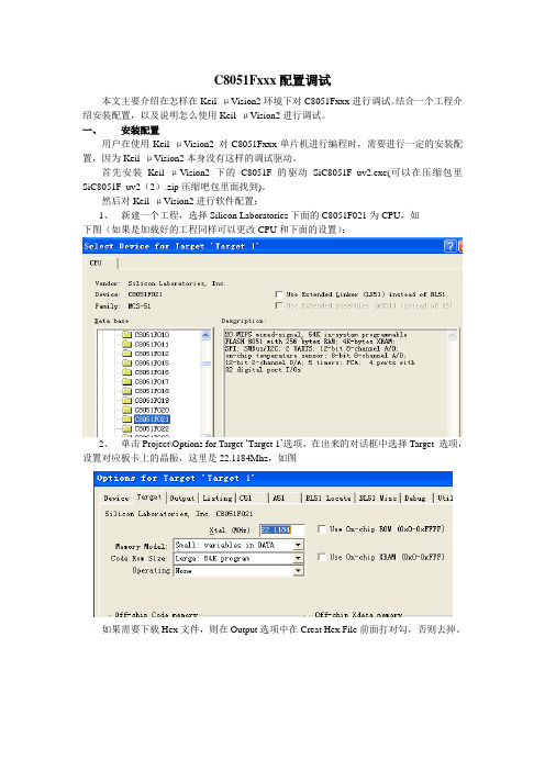
然后对Keil μVision2进行软件配置:1、新建一个工程,选择Silicon Laboratories下面的C8051F021为CPU,如下图(如果是加载好的工程同样可以更改CPU和下面的设置):2、单击Project\Options for Target ‘Target 1’选项,在出来的对话框中选择Target 选项,设置对应板卡上的晶振,这里是22.1184Mhz,如图如果需要下载Hex文件,则在Output选项中在Creat Hex File前面打对勾,否则去掉。
点击Debug选项,选择应用use Silicon Labs C8051Fxxx Drivers,选择Go till main。
如图:如果需要则在Setting中设置相应的端口和波特率。
由于使用是调试适配器用的是USB 口,且驱动是人体学输入设备,所以不用选择。
3、至此安装设置完成,可以使用Keil μVision2对C8051Fxxx系列单片机进行编写、编译、下载和运行程序。
二、相关操作1、编写程序在工程里面编写并添加程序,首先是新建一个C文件或者ASM文件:点击菜单栏中的file\new…打开编写程序的对话框,点击保存,弹出对话框进行保存,要编写成C文件后缀名为.C,如果是汇编语言则后缀名为.ASM,然后保存。
如下图:这就可以在文本对话框中进行程序编写了。
- 1、下载文档前请自行甄别文档内容的完整性,平台不提供额外的编辑、内容补充、找答案等附加服务。
- 2、"仅部分预览"的文档,不可在线预览部分如存在完整性等问题,可反馈申请退款(可完整预览的文档不适用该条件!)。
- 3、如文档侵犯您的权益,请联系客服反馈,我们会尽快为您处理(人工客服工作时间:9:00-18:30)。
关于开发工具及调试的技术问答
1、问:C8051FXX系列单片机的开发工具是不是串行适配器(PC机串口和JTAG协议转换适配)相同而目标版不同?
答:开发套件中串行适配器(核心部件)是通用的,只是目标版不同。
只要您购买一套开发套件,就可以开发全系列单片机,只要将集成开发环境软件升级就可以了。
为了加快您的开发进程,您只要购买带有相关型号单片机的目标板就可以了。
2、问:C8051F单片机是怎样调试用户系统的?
答:C8051F单片机是用开发套件来调试用户系统的。
单片机开发套件包括开发软件IDE(集成开发环境),ML-EC3至PC机USB口和单片机JTAG接口的协议转换模块和一个目标板(板上有
C8051FMCU)。
IDE中集成编译器,汇编器和连接器,支持汇编语言和C语言(第三方支持);ML-EC3是从USB口到JTAG协议的转换模块。
目标板上带有一块相应的C8051FMCU和一些简单的外围电路构成一个最小单片机系统,并将所有引脚连接到插座。
C8051F单片机内集成了一个以JTAG协议为基础的调试电路,这样在调试您的系统时,不需要专用仿真芯片、目标仿真头及目标RAM等。
您在IDE上编译生成程序代码后,通过ML-EC3(连接到计算机USB口和JTAG接口)将代码下载到用户系统板的C8051FMCU的Flash存储器中,然后您就可以调试您的目标系了。
3、问:可以用KeiluVision2IDE调试全系列C8051F单片机应用系统吗?
答:可以。
但必须安装动态链接库。
该驱动程序可以在我公司的网站上下载。
4、问:如何将绝对目标代码转换成hex格式文件?
答:第一,可以使用KEILC,在编译时直接生成。
第二,使用OH51(DOS命令)将目标文件转换成hex格式的文件。
Oh5Linputfile〔hexfile〕
第三,在IDE环境中生成HEX文件
﹙1﹚.在TOOL菜单中选择ADDREMOVEUSERTOOL
﹙2﹚.点击ADD按钮,增加一个MENUTEXT(名称可以任何输入)
﹙3﹚.在TOOLS里选择OH51.EXE文件(此文件在KEIL的BIN目录中有,必须将此文件放在项目所在目录)
﹙4﹚.在ARGUMENTS里输入文件名或项目名
﹙5﹚.在DIROF里输入HEX文件的保存目录
5、问:Silabs IDE中带有4K代码限制版的KeilC51,那么如何将无限制版的KeilC51嵌入到Silabs IDE中呢?
答:先将您完全版的KeilC51安装到您的PC机中;然后进入Silabs IDE界面,选择Project-﹥TOOLChainIntegration弹出对话框,单击Browse按钮,更换A51.EXE和BL51.EXE的路径(换成“Keil安装目录”/c51/bin)即可。
6、问:程序代码加密后,IDE不能与目标系统连接怎么办?
答:进入IDE界面,选择Tools→EraseSpace来擦除FLASH后,自动与目标系统连接。