MPC5604B单片机开发工具套装说明书
TRK-MPC5604B Quick Start Guide _REV 0_中文

1.开始认识TRK-MPC5604BTRK-MPC5604BFreescale StarterTRAKTRK-MPC5604B开发板是飞思卡尔StarterTRAK系列的一员。
它是一个带有快速原型和可复用的工具特点的开发平台。
今天你可以带着你的设计到下一个阶段,同时开始构建你的StarterTRAK系统。
2.TRK- MPC5604B的特点● MPC560xB/C系列微控制器(144-pin LQFP)● 板上JTAG连接,通过开源的使用MPC9S08JM微控制器的OSBDM电路源代码参考/osbdm● MCZ3390S5EK系统基础芯片,带有先进的电源管理和集成CAN控制器和LIN2.0接口● CAN接口● LIN接口● 模拟量接口,带有电位器● 高效能LED● SCI串行通信接口3.安装说明在这个快速启动向导里面,你将可以学习怎样设置TRK-MPC5604B开发板和运行默认的低功耗实验室案例。
安装软件和工具● 安装CodeWarrior Development Studio for 55xx/56xx Architectures v2.7或以上版本● 安装RAppID初始化工具按顺序安装。
这些程序在DVD里面。
CodeWarrior和RAppID包括一个30天的评估版许可证。
如果有升级,请参考/StarterTRAK连接USB线连接USB线的一端到电脑,另一端到TRK-MPC5604B开发板上的mini-B连接器。
如果需要,允许电脑自动识别USB驱动。
打开支持文档从DVD光盘上的documentation和Training文件夹里面打开《MPC5500 and MPC5600 Simple Cookbook》和《TRK-MPC5604B User Manual》。
浏览更多MPC5500和MPC5600案例:低功耗实验室案例要运行一个使用TRK-MPC5604B的例程,按照《MPC5500 and MPC5600 Simple Cookbook》上面低功耗实验室例子的说明。
基于32位微控制器MPC5604的双离合器.自动变速器控制系统
【 s a tT ecnrlss m o ul ltht nmi i ei e ae n 3 一 i Mi oot l rMP 5 0 . Abt c]h o t yt f a cuc a s s o i d s n db sdo 2 bt c cn ol C 64 r o e d r sn s g r r e
变 速器 ( u l lthTa s si . C ) 电控 单 元 D a Cuc rnmi o D T sn ( rn m sinC nrl n , C T a s i o o t i T U)是 实 现 D T车 辆 s oU t C 整车 及 自动变 速 控制 的基 础 。 随着需 求 的不 断增加 . 微 控 制器 作 为 T U的 核心 .其 功 能 1 复杂 化 . C 3趋 目 前 常用 的 8位 、6位 微控 制 器 由 于数 据 处 理 能 力 、 1
p o e s rc s ・
.
Ke r s Du lcu c r n m is n Co to y tm , 2 b tmir c n r l r y wo d : a lth ta s si , n r l se o s 3- i c o o tol e
1 前 言
具有 高精 度 、 高速 度 、 高可靠 性 的双 离合 器 自动
M ir c n r l r M PC5 0 c o o tol e 64
S in u , u Gu n q a g 。 iJa y 。 W a g in ’
( . n jU ie i ; . o y nvri ) 1 o g nvr t 2 T k oU ie t T i sy s y
主题 词 : 离合 器 自动变 速器 双
控 制 系统
MEGAWIN MPC89LE51_52_53_54_58_515 说明书
8051内核-单片机This document contains information on a new product under development by Megawin. Megawin reserves the right to change or discontinue this product without notice.Megawin Technology Co., Ltd. 2005 All rights reserved.2015/09 version A1.02MPC89LE51_52_53_54_58_515規格书版本: A1.022MPC89LE51_52_53_54_58_515 说明书MEGAWIN特性●80C51内核●可选12T或6T模式●最大工作频率位48MHz@12T或24MHz@6T●程序空间: MPC89E/L51(4KB),MPC89E/L52(8KB),MPC89E/L53(15KB),MPC89E/L54(16KB)MPC89E/L58(32KB),MPC89E/L515(63KB)●ISP空间大小;可选1K/2K/4K ISP空间,对于MPC89x51/52/53/54/58是与数据空间共享,而MPC89x53/515是与应用程序空间共享●IAP空间大小;MPC89x51: 最大到10KB,与ISP空间共享数据空间MPC89x52: 最大到6KB,与ISP空间共享数据空间MPC89x53: 无MPC89x54: 最大到46KB,与ISP空间共享数据空间MPC89x58: 最大到30KB,与ISP空间共享数据空间MPC89x515: 无注: 要使用IAP,必须设置ISP空间最小为1K。
●内嵌外部寻址RAM(XDATA), MPC89x51/52/53(256Byte),MPC89x54/58/515(1024Byte);●两级代码加密保护●三个16位定时/计数器, Timer2是一个向上/向下计数器,可编程时钟输出在P1.0口上●8个中断源,4级优先级●一组增强型UART, 提供帧错误检测和硬件地址识别●双DPTR●15位看门狗,8位预分频。
C8051F00x 01x开发套件用户指南说明书
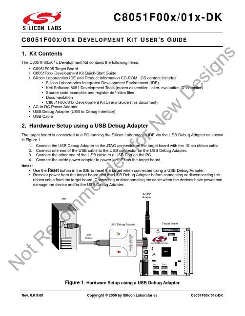
Rev. 0.6 9/06Copyright © 2006 by Silicon LaboratoriesC8051F00x/01x-DKX X E VE LO P M E N T I T S E R S UI D E1. Kit ContentsThe C8051F00x/01x Development Kit contains the following items:•C8051F005 Target Board•C8051Fxxx Development Kit Quick-Start Guide•Silicon Laboratories IDE and Product Information CD-ROM. CD content includes:•Silicon Laboratories Integrated Development Environment (IDE)•Keil Software 8051 Development Tools (macro assembler, linker, evaluation ‘C’ compiler)•Source code examples and register definition files •Documentation•C8051F00x/01x Development Kit User’s Guide (this document)•AC to DC Power Adapter•USB Debug Adapter (USB to Debug Interface)•USB Cable2. Hardware Setup using a USB Debug AdapterThe target board is connected to a PC running the Silicon Laboratories IDE via the USB Debug Adapter as shown in Figure 1.1.Connect the USB Debug Adapter to the JTAG connector on the target board with the 10-pin ribbon cable.2.Connect one end of the USB cable to the USB connector on the USB Debug Adapter.3.Connect the other end of the USB cable to a USB Port on the PC.4.Connect the ac/dc power adapter to power jack P1 on the target board.Notes:•Use the Reset button in the IDE to reset the target when connected using a USB Debug Adapter.•Remove power from the target board and the USB Debug Adapter before connecting or disconnecting the ribbon cable from the target board. Connecting or disconnecting the cable when the devices have power can damage the device and/or the USB Debug Adapter.Figure 1. Hardware Setup using a USB Debug AdapterPWRP1.6No tR nd edf or N e wDe si g n sC8051F00x/01x-DK3. Software SetupThe included CD-ROM contains the Silicon Laboratories Integrated Development Environment (IDE), Keil software 8051 tools and additional documentation. Insert the CD-ROM into your PC’s CD-ROM drive. An installer will auto-matically launch, allowing you to install the IDE software or read documentation by clicking buttons on the Installa-tion Panel. If the installer does not automatically start when you insert the CD-ROM, run autorun.exe found in the root directory of the CD-ROM. Refer to the readme.txt file on the CD-ROM for the latest information regarding known IDE problems and restrictions.4. Silicon Laboratories Integrated Development EnvironmentThe Silicon Laboratories IDE integrates a source-code editor, source-level debugger and in-system Flash program-mer. The use of third-party compilers and assemblers is also supported. This development kit includes the Keil Software A51 macro assembler, BL51 linker and evaluation version C51 ‘C’ compiler. These tools can be used from within the Silicon Laboratories IDE.4.1. System RequirementsThe Silicon Laboratories IDE requirements:•Pentium-class host PC running Microsoft Windows 98SE or later.•One available COM or USB port.•64 MB RAM and 40MB free HD space recommended.4.2. Assembler and LinkerA full-version Keil A51 macro assembler and BL51 banking linker are included with the development kit and are installed during IDE installation. The complete assembler and linker reference manual can be found under the Help menu in the IDE or in the “SiLabs\MCU\hlp ” directory (A51.pdf).4.3. Evaluation C51 ‘C’ CompilerAn evaluation version of the Keil C51 ‘C’ compiler is included with the development kit and is installed during IDE installation. The evaluation version of the C51 compiler is the same as the full professional version except code size is limited to 4kB and the floating point library is not included. The C51 compiler reference manual can be found under the Help menu in the IDE or in the “SiLabs\MCU\hlp ” directory (C51.pdf).4.4. Using the Keil Software 8051 Tools with the Silicon Laboratories IDETo perform source-level debugging with the IDE, you must configure the Keil 8051 tools to generate an absolute object file in the OMF-51 format with object extensions and debug records enabled. You may build the OMF-51absolute object file by calling the Keil 8051 tools at the command line (e.g. batch file or make file) or by using the project manager built into the IDE. The default configuration when using the Silicon Laboratories IDE project manager enables object extension and debug record generation. Refer to Applications Note AN104 - Integrating Keil 8051 Tools Into the Silicon Labs IDE in the “SiLabs\MCU\Documentation\Appnotes ” directory on the CD-ROM for additional information on using the Keil 8051 tools with the Silicon Laboratories IDE.To build an absolute object file using the Silicon Laboratories IDE project manager, you must first create a project. A project consists of a set of files, IDE configuration, debug views, and a target build configuration (list of files and tool configurations used as input to the assembler, compiler, and linker when building an output object file).The following sections illustrate the steps necessary to manually create a project with one or more source files, build a program and download the program to the target in preparation for debugging. (The IDE will automatically create a single-file project using the currently open and active source file if you select Build/Make Project before a project is defined.)No tR e co mme nd edf or N e wDe si g n sC8051F00x/01x-DK4.4.1. Creating a New Project1.Select Project →New Project to open a new project and reset all configuration settings to default.2.Select File →New File to open an editor window. Create your source file(s) and save the file(s) with a rec-ognized extension, such as .c, .h, or .asm, to enable color syntax highlighting.3.Right-click on “New Project” in the Project Window . Select Add files to project . Select files in the filebrowser and click Open. Continue adding files until all project files have been added.4.For each of the files in the Project Window that you want assembled, compiled and linked into the targetbuild, right-click on the file name and select Add file to build . Each file will be assembled or compiled as appropriate (based on file extension) and linked into the build of the absolute object file.Note: If a project contains a large number of files, the “Group” feature of the IDE can be used to organize. Right-click on “New Project” in the Project Window . Select Add Groups to project . Add pre-definedgroups or add customized groups. Right-click on the group name and choose Add file to group . Select files to be added. Continue adding files until all project files have been added.4.4.2. Building and Downloading the Program for Debugging1.Once all source files have been added to the target build, build the project by clicking on the Build/MakeProject button in the toolbar or selecting Project →Build/Make Project from the menu.Note: After the project has been built the first time, the Build/Make Project command will only build the files that have been changed since the previous build. To rebuild all files and project dependencies, click on the Rebuild All button in the toolbar or select Project →Rebuild All from the menu.2.Before connecting to the target device, several connection options may need to be set. Open theConnection Options window by selecting Options →Connection Options... in the IDE menu. First, select the appropriate adapter in the “Serial Adapter” section. Next, the correct “Debug Interface” must be selected.C8051F00x/01x family devices use the JTAG debug interface. Once all the selections are made, click the OK button to close the window. 3.Click the Connect button in the toolbar or select Debug →Connect from the menu to connect to the device.4.Download the project to the target by clicking the Download Code button in the toolbar.Note: To enable automatic downloading if the program build is successful select Enable automatic con-nect/download after build in the Project →Target Build Configuration dialog. If errors occur during the build process, the IDE will not attempt the download.5.Save the project when finished with the debug session to preserve the current target build configuration,editor settings and the location of all open debug views. To save the project, select Project->Save Project As... from the menu. Create a new name for the project and click on Save .No tR e co mme nd edf or N e wDe si g n sC8051F00x/01x-DK5. Example Source CodeExample source code and register definition files are provided in the “SiLabs\MCU\Examples\C8051F0xx ” directory during IDE installation. These files may be used as a template for code development. Example applications include a blinking LED example which configures the green LED on the target board to blink at a fixed rate.5.1. Register Definition FilesRegister definition files C8051F000.inc and C8051F000.h define all SFR registers and bit-addressable control/status bits for the C8051F00x/01x device family. They are installed into the “SiLabs\MCU\Examples\C8051F0xx ” directory during IDE installation. The register and bit names are identical to those used in the C8051F00x/01x data sheet. Both register definition files are also installed in the default search path used by the Keil Software 8051 tools. Therefore, when using the Keil 8051 tools included with the development kit (A51, C51), it is not necessary to copy a register definition file to each project’s file directory.5.2. Blinking LED ExampleThe example source files blink.asm and blinky.c show examples of several basic C8051F00x/01x functions. These include; disabling the watchdog timer (WDT), configuring the Port I/O crossbar, configuring a timer for an interrupt routine, initializing the system clock, and configuring a GPIO port. When compiled/assembled and linked this pro-gram flashes the green LED on the target board about five times a second using the interrupt handler with a timer.No tR e co mme nd edf or N e wDe si g n sC8051F00x/01x-DK6. Target BoardThe C8051F00x/01x Development Kit includes a target board with a C8051F005 device pre-installed for evaluation and preliminary software development. Numerous input/output (I/O) connections are provided to facilitate prototyp-ing using the target board. Refer to Figure 2 for the locations of the various I/O connectors.P1Power connector (accepts input from 7 to 15 VDC unregulated power adapter)J1Connects SW2 to port pin P1.7J264-pin I/O connector providing access to all I/O signals J3Connects LED D3 to port pin P1.6J4JTAG connector for Debug Adapter interface J6Analog I/O configuration connector X1Analog I/O terminal blockFigure 2. C8051F005 Target BoardNo tR e si g n sC8051F00x/01x-DK6.1. System Clock SourcesThe C8051F005 device installed on the target board features a internal oscillator which is enabled as the system clock source on reset. After reset, the internal oscillator operates at a frequency of 2MHz (±2%) by default but may be configured by software to operate at other frequencies. Therefore, in many applications an external oscillator is not required. However, an external crystal may be installed on the target board for additional applications. The tar-get board is designed to facilitate the installation of an external crystal at the pads marked Q1. Refer to the C8051F005 datasheet for more information on configuring the system clock source. Following are a few part num-bers of suitable crystals:Freq (MHz)Digikey P/N ECS P/N18.432X146-ND ECS-184-20-1 (20pF loading capacitance)11.0592X089-ND ECS-110.5-20-1(20pF loading capacitance)6.2. Switches and LEDsTwo switches are provided on the target board. Switch SW1 is connected to the RESET pin of the C8051F005device on the target board. Pressing SW1 puts the device into its hardware-reset state. The device will leave the reset state after SW1 is released. Switch SW2 is connected to the device’s general purpose I/O (GPIO) pin through headers. Pressing SW2 generates a logic low signal on the port pin. Remove the shorting block from the header to disconnect SW2 from the port pins. The port pin signal is also routed to a pin on the J2 I/O connector. See Table 1 for the port pins and headers corresponding to each switch.Two LEDs are also provided on the target board. The red LED labeled PWR is used to indicate a power connection to the target board. The green LED labeled with a port pin name is connected to the device’s GPIO pin through a header. Remove the shorting block from the header to disconnect the LED from the port pin. The port pin signal is also routed to a pin on the J2 I/O connector. See Table 1 for the port pins and headers corresponding to each LED.6.3. Target Board JTAG Interface (J4)The JTAG connector (J4) provides access to the JTAG pins of the C8051F005. It is used to connect the Serial Adapter or the USB Debug Adapter to the target board for in-circuit debugging and Flash programming. Table 2 shows the JTAG pin definitions.Table 1. Target Board I/O DescriptionsDescriptionI/OHeaderSW1Reset none SW2P3.7J1Green LED P1.6J3Red LEDPWRnoneTable 2. JTAG Connector Pin DescriptionsPin #Description1+3VD (+3.3VDC)2, 3, 9GND (Ground)4TCK 5TMS 6TDO 7TDI8, 10Not ConnectedNo tR e co mme nd edf or N e wDe si gn sC8051F00x/01x-DK6.4. Analog I/O (J6, Terminal Block)An Analog I/O Configuration connector (J6) provides the ability to route analog I/O signals from the C8051F005device to a terminal block by installing two shorting blocks on J6. It also allows the DAC outputs to be connected to Comparator 0 inputs or to two ADC inputs. Analog signals may be routed to the AIO 0 and AI01 posts of the termi-nal block by installing a shorting block between two adjacent pins on J6. Refer to Figure 3 to determine the shorting block installation positions required to connect the desired analog signal to the terminal block. Refer to Table 3 for terminal block connections and Table 4 for J6 pin definitions.Figure 3. J6 Analog I/O Configuration ConnectorTable 3. Terminal Block Pin DescriptionsPin #Description1AIO12AIO07AGND (Analog Ground)8VREFTable 4. J6 Connector Pin DescriptionsPin #Description1CP0+2CP0-3, 9, 15AIO14, 10, 16AIO05DAC06DAC17AIN08AIN111AIN212AIN313AIN414AIN517AIN618AIN7No tR e co mme nd edf or N De si g n sC8051F00x/01x-DK6.5. Expansion I/O Connector (J2)The 64-pin expansion I/O connector J1 provides access to most signal pins of the C8051F005 device on the target board. A small through-hole prototyping area is also provided. All I/O signals routed to connector J2 are also routed to through-hole connection points between J2 and the prototyping area (see Figure 4 on page 9). The signal layout pat-tern of these connection points is identical to the adjacent J2 connector pins . See Table 5 for a list of pin descrip-tions for J2.Table 5: J2 Pin DescriptionsPin DescriptionPin Description 1+VD (digital voltage supply)28P3.72XTAL129P3.43P1.630P3.54P1.731P3.25P1.432P3.36P1.533P3.07P1.234P3.18P1.336/RST9P1.039,41,42GND (digital ground)10P1.145,47,63GNDA (analog ground)11P0.646,64+VA (analog voltage supply)12P0.748DAC013P0.449CP1-14P0.550DAC115P0.251CP1+16P0.352CP0-17P0.053VREF 18P0.154CP0+19P2.655AIN020P2.756AIN121P2.457AIN222P2.558AIN323P2.259AIN424P2.360AIN525P2.061AIN626P2.162AIN727P3.6No tR e co mme nd edf or N e wDe si g n sC8051F00x/01x-DKC8051F00x/01x-DKD OCUMENT C HANGE L ISTRevision 0.4 to Revision 0.5⏹Section 1, added USB Debug Adapter and USB Cable.⏹Section 2, changed name from "Hardware Setup" to "Hardware Setup using an EC2 Serial Adapter".⏹Section 2, added 2 Notes bullets.⏹Section 2, removed Note from bottom of page.⏹Added Section 3, "Hardware Setup using a USB Debug Adapter".⏹Section 5.4.2, changed step 2 to include new instructions.⏹Section 7, J4, changed "Serial Adapter" to "Debug Adapter".⏹Target Board DEBUG Interface Section, added USB Debug Adapter.⏹DEBUG Connector Pin Descriptions Table, changed pin 4 to C2D.⏹Changed "jumper" to "header".⏹EC2 Serial Adapter section, added EC2 to the section title, table title and figure title.⏹EC2 Serial Adapter section, changed "JTAG" to "DEBUG".⏹Added "USB Debug Adapter" section.Revision 0.5 to Revision 0.6⏹Removed EC2 Serial Adapter from Kit Contents.⏹Removed Section 2. Hardware Setup using an EC2 Serial Adapter. See RS232 Serial Adapter (EC2) User's Guide.⏹Removed Section 8. EC2 Serial Adapter. See RS232 Serial Adapter (EC2) User's Guide.⏹Removed Section 9. USB Debug Adapter. See USB Debug Adapter User's Guide.No tR e co mme nd edf or N e wDe si g n sDisclaimer Silicon Laboratories intends to provide customers with the latest, accurate, and in-depth documentation of all peripherals and modules available for system and software implementers using or intending to use the Silicon Laboratories products. Characterization data, available modules and peripherals, memory sizes and memory addresses refer to each specific device, and "Typical" parameters provided can and do vary in different applications. Application examples described herein are for illustrative purposes only. Silicon Laboratories reserves the right to make changes without further notice and limitation to product information, specifications, and descriptions herein, and does not give warranties as to the accuracy or completeness of the included information. Silicon Laboratories shall have no liability for the consequences of use of the information supplied herein. This document does not imply or express copyright licenses granted hereunder to design or fabricate any integrated circuits. The products must not be used within any Life Support System without the specific written consent of Silicon Laboratories. A "Life Support System" is any product or system intended to support or sustain life and/or health, which, if it fails, can be reasonably expected to result in significant personal injury or death. Silicon Laboratories products are generally not intended for military applications. Silicon Laboratories products shall under no circumstances be used in weapons of mass destruction including (but not limited to) nuclear, biological or chemical weapons, or missiles capable of delivering such weapons.Trademark InformationSilicon Laboratories Inc., Silicon Laboratories, Silicon Labs, SiLabs and the Silicon Labs logo, CMEMS®, EFM, EFM32, EFR, Energy Micro, Energy Micro logo and combinations thereof, "the world’s most energy friendly microcontrollers", Ember®, EZLink®, EZMac®, EZRadio®, EZRadioPRO®, DSPLL®, ISOmodem ®, Precision32®, ProSLIC®, SiPHY®, USBXpress® and others are trademarks or registered trademarks of Silicon Laboratories Inc. ARM, CORTEX, Cortex-M3 and THUMB are trademarks or registered trademarks of ARM Holdings. Keil is a registered trademark of ARM Limited. All other products or brand names mentioned herein are trademarks of their respective holders. Silicon Laboratories Inc.400 West Cesar ChavezAustin, TX 78701USAIoT Portfolio /IoT SW/HW /simplicity Quality /quality Support and Community N o t R e co m m e nd e d f o r N e w D e s i g n s。
MPC56XXEUB使用说明
密级:MPC56XXEUB使用说明哈尔滨工业大学汽车电子工程中心HIT Automotive Electronic Engineering Center文档历史记录注:1.文件编号和受控编号在服务器incoming \文档管理\文件编号中查询;2.版本号格式:Ver xxxx,例:Ver 1.0 或Ver. 1.0.1。
若未形成正式版本,标注为:Draft3.日期格式:年-月-日,例:2007-03-30在“修订情况”栏中详细说明;4.第一稿不填情况说明,以后无论正式版还是Draft 版,均说明修订的地方(如增加条款,删减条款、修订条款);5.需要进一步说明的内容在备注栏中说明。
目录1引言(INTRODUCTION) (1)1.1编写目的(Purpose) (1)1.2参考文档(References) (1)1.3缩略语(Abbreviations/Acronyms) (1)2跳线大头针排序(PIN NUMBERING FOR JUMPERS) (1)3供电方式(POWER SUPPLIES) (1)3.1J3(Jumper J3) (2)3.1.1J3 转换速率配置(适用于版本C)(Slew Rate Select) (2)3.2J4(Jumper J4) (2)3.3J5(Jumper J5) (2)3.3.1J5 电源重置时,输出电压置位值(适用于版本C)(Power Reset Pullup V oltage Select) (2)3.4J6(Jumper J6) (2)3.4.1J6 电源重置输出使能位(Power Reset Output Enable) (2)3.5J7(Jumper J7) (2)3.5.1J7 VPROG调整器控制(适用于版本C)(VPROG Regulators Control) (2)3.6J37(Jumper J37) (3)3.6.1J37 低电压探测器(VBat Low V oltage Detection) (3)3.7J41(Jumper J41) (3)3.7.1J41 电源重置拉升使能位(适用于版本C)(Power Reset Pullup Enable) (3)4母板与最小系统板及MCU安装方式(INSTALLING MINI-MODULE AND MCU) (3)5各跳线功能(JUMPERS EFFECT) (3)5.1LEDs (3)5.1.1J8——LEDS使能位(Enable) (3)5.2Buttons (4)5.2.1J9——按键使能位(Buttons Enable) (4)5.2.2J10——按键驱动配置(Button Driving Configuration) (4)5.2.3J11——按键空闲配置(Button Idle Configuration) (4)5.3LIN (5)5.3.1J15——LIN1 VSUP 配置(Configuration) (5)5.3.2J13——LIN1 使能(Enable) (5)5.3.3J16——LIN1 控制选择(Master Selection) (5)5.3.4J14——LIN1 VBUS 配置(Configuration) (5)5.3.5J25——LIN1/SCI TxD 选择(TxD Selection) (5)5.3.6J22——LIN1/SCI RxD选择(RxD Selection) (6)5.3.7J20——LIN2 VSUP配置(VSUP Configuration) (6)5.3.8J17——LIN2 使能(Enable) (6)5.3.9J21——LIN2 控制选择(Master Selection) (6)5.3.10J18——LIN2 VBUS 配置(VBUS Configuration) (7)5.3.11J19——LIN2/SCI TxD选择(TxD Selection) (7)5.3.12J12——LIN2/SCI RxD选择(RxD Selection) (7)5.4SCI (7)5.4.1J24——SCI TxD使能(TxD Enable) (7)5.4.2J23——SCI RxD使能(RxD Enable) (8)5.5CAN (8)5.5.1J28——CAN(H)传输使能(Transmit Enable) (8)5.5.2J27——CAN(H)TxD/RxD使能(TxD/RxD Enable) (8)5.5.3J30——CAN(L)使能(Enable) (8)5.5.4J31——CAN(L) CTE(Jumper J31) (9)5.5.5J29——CAN(L) TxD/RxD使能(TxD/RxD Enable) (9)5.6FlexRay (9)5.6.1J32——FlexRay总线驱动1使能(Bus Driver 1 Enable) (10)5.6.2J35——FlexRay总线驱动1配置(Bus Driver 1 Configuration) (10)5.6.3J33 & J34 FlexRay 1 终端电阻器连接(Terminal Resistor Connection) (10)5.6.4J36——FlexRay总线驱动2使能(Bus Driver 2 Enable) (10)5.6.5J39——FlexRay总线驱动2配置(Bus Driver 2 Configuration) (11)5.6.6J37 & J38 FlexRay 2 终端电阻器连接(Terminal Resistor Connection) (11)5.7电位计(Potentiometer) (11)5.7.1J40——POT使能(POT Enable) (12)1引言(Introduction)1.1编写目的(Purpose)为了更好的使用MPC 56XXEUB以及与之配套的单片机,特编写此使用说明。
电子科技大学研究生嵌入式系统实验03
SetRelAlarm(Alarm200ms, 0, 200);
SetRelAlarm(Alarm500ms, 0, 500);
SetRelAlarm(Alarm1000ms, 0, 1000);
/*设置转换组0的结果缓存*/
Adc_SetupResultBuffer(0, &adc_buffer[0]);
0 ,
0,
0,
15,
1
},
{
(T_OSEK_TASK_Entry)FuncTask200ms,
Task200ms,
0 , //
0,
0,
14,
1
},
{
(T_OSEK_TASK_Entry)FuncTask500ms,
Task500ms,
0 ,
0,
0,
13,
1
},
{
(T_OSEK_TASK_Entry)FuncTask1000ms,
{
{
Task1ms,
#if (defined(OCC_ECC1) || defined(OCC_ECC2)) && defined(OCC_ALMSETEVENT)
0,
#endif
Counter1,
},
{
Task10ms,
#if (defined(OCC_ECC1) || defined(OCC_ECC2)) && defined(OCC_ALMSETEVENT)
MPC5634开发板接收,后者又将收到的字符重新通过串口输出。
本测试程序的目的是为验证MPC5634上的SCI驱动程序的正确性,主要验证其
MPC5604PCBUM
Freescale Semiconductor MPC5604P Controller BoardUsers ManualOrder this document byMPC5604PCBUMRev. 0, 05/2009Table of ContentsIntroduction 61.1MPC5604P Controller Board Architecture . . . . . . . . . . . . . . . . . . . . . . . . . . . . . . . 61.2MPC5604P Controller Board Configuration Jumpers . . . . . . . . . . . . . . . . . . . . . . 71.3About this Manual . . . . . . . . . . . . . . . . . . . . . . . . . . . . . . . . . . . . . . . . . . . . . . . . 101.4Setup Guide . . . . . . . . . . . . . . . . . . . . . . . . . . . . . . . . . . . . . . . . . . . . . . . . . . . . . 11Operational Description 122.1Introduction . . . . . . . . . . . . . . . . . . . . . . . . . . . . . . . . . . . . . . . . . . . . . . . . . . . . . 122.2Electrical Characteristics . . . . . . . . . . . . . . . . . . . . . . . . . . . . . . . . . . . . . . . . . . . 13Pin Description 143.1Introduction . . . . . . . . . . . . . . . . . . . . . . . . . . . . . . . . . . . . . . . . . . . . . . . . . . . . . 143.2Signal Description . . . . . . . . . . . . . . . . . . . . . . . . . . . . . . . . . . . . . . . . . . . . . . . . 14Design Consideration 234.1Overview . . . . . . . . . . . . . . . . . . . . . . . . . . . . . . . . . . . . . . . . . . . . . . . . . . . . . . . 234.2MPC5604P . . . . . . . . . . . . . . . . . . . . . . . . . . . . . . . . . . . . . . . . . . . . . . . . . . . . . 234.3Clock Source . . . . . . . . . . . . . . . . . . . . . . . . . . . . . . . . . . . . . . . . . . . . . . . . . . . . 244.4UNI3 Interface and External Fault Management . . . . . . . . . . . . . . . . . . . . . . . . . 254.5Encoder Inputs . . . . . . . . . . . . . . . . . . . . . . . . . . . . . . . . . . . . . . . . . . . . . . . . . . 264.6Resolver and SINCOS Sensor . . . . . . . . . . . . . . . . . . . . . . . . . . . . . . . . . . . . . . 274.7Analog Signal Sensing . . . . . . . . . . . . . . . . . . . . . . . . . . . . . . . . . . . . . . . . . . . . 274.8Power Supplies and Voltage Reference . . . . . . . . . . . . . . . . . . . . . . . . . . . . . . . . 284.9UNI-3 PFC-PWM Signal (Power Factor Correction) . . . . . . . . . . . . . . . . . . . . . . 284.10UNI-3 Brake Signal . . . . . . . . . . . . . . . . . . . . . . . . . . . . . . . . . . . . . . . . . . . . . . . 294.11CAN and SafetyCAN Bus . . . . . . . . . . . . . . . . . . . . . . . . . . . . . . . . . . . . . . . . . . 294.12FlexRAY Interface . . . . . . . . . . . . . . . . . . . . . . . . . . . . . . . . . . . . . . . . . . . . . . . . 29MCPC5604P Controller Board Schematics 30Bill of Materials 42by: Petr KonvicnyFreescale SemiconductorCzech System CenterTo provide the most up-to-date information, the revision of our documents on the world-wide web will be the most current. Your printed copy may be an earlier revision. To verify that you have the latest information available, refer to .The following revision history table summarizes the changes contained in this document. For your convenience, the page number designators have been linked to the appropriate location.Revision HistoryTable0-1 Revision History TableDate RevisionlevelDescriptionPagenumber(s)6.3.20090Initial release N/ASection1. Introduction Freescale Semiconductor MPC5604P controller board is an embeded controller board integrated to Freescale Semiconductor embedded motion-control series of development tools. It provides controller functions for 3-phase BLDC, PMSM, and ACIM motors. It is supplied with a 40-pin ribbon cable interconnecting with, among others, one of the embedded motion-power stages or evaluation boards, providing a ready-made software-development platform for small permanent-magnet synchronous or brushless DC motors.The MPC5604P controller board is an evaluation-module type of board which includes an MPC5604P device, an encoder interface, resolver, sin/cos interface, communications options, digital and analog power supplies, and peripheral expansion connectors. The expansion connectors are intended for signal monitoring and user expandability. Test pads are provided for monitoring critical signals and voltage levels.1.1 MPC5604P Controller Board ArchitectureThe MPC5604P controller board facilitates the evaluation of various features present in the MPC5604P. It can be used to develop real-time software and hardware products based on MPC5604P. It provides the features neccesary for the user to write and debug software, demonstrate the functionality of that software, and to interface with the customer’s application specific device(s). The UNI-3 expansion connector enables this board to directly interface with the most of Freescale motor-control demo power stages. The MPC5604P controller board is flexible enough to allow the users to fully exploit the MPC5604P features to optimize the performance of their product, as shown in Figure1-1.Figure1-1 Controller Board Block Diagram1.2 MPC5604P Controller Board Configuration JumpersJumper groups and zero Ohm resistors1 shown in fig are used to configure various features on the MPC5604P controller board.1. Zero Ohm resistors are used instead of standard jumpers to minimize the distortion of analog signals, and to achieve a high signal-to-noise ratio.Table1-1 MPC5604P Controller Board Jumper Options#Selector Function Connections JP1,JP2CAN Terminate CAN bus node.closedJP104MC33905debug modeEnter SBC driver MC33905 to debug mode.closedJP105MC33905save modeEnter SBC driver MC33905 to safe mode.closedJP200Resolver Enable Resolver reference input signal from MCU disabled.open Resolver reference input signal from MCU enabled.closedJ203Resolver SINinputPositive input for SIN OPAM is DC offset voltage set up bytrimmer R209.1–2 Positive input for SIN OPAM is REFSIN input of resolver.2–3J204Resolver COSinputPositive input for COS OPAM is DC offset voltage set up bytrimmer R209.1–2 Positive input for COS OPAM is REFCOS input of resolver.2–3J205Phase Adigital signalResolver Phase A signal is connected to GPIO F[13].1–2SIN/COS Phase A signal is connected to GPIO F[13].2–3J206Phase Bdigital signalResolver Phase A signal is connected to GPIO A[5].1–2SIN/COS Phase A signal is connected to GPIO A[5].2–3J2Resolverinput signalResolver reference signal is generated by GPIO C[11].2–3Resolver reference signal is generated by GPIO C[12].1–2J301FAULT1selectionUNI-3 Phase A over-current signal is connected to FAULT1 inputG[9].1–2UNI-3 DC-bus over-current signal is connected to FAULT1 inputG[9].2–3J312BOOT selection MPC5604P boot from internal Flash.closedJ500Encoder 0Phase AEncoder0 JP500 pin three PHASE A input signal is connected toGPIO A[0].1–2 UNI-3 BEMFZCA input signal is connected to GPIO A[0].2–3J501Encoder 0Phase BEncoder0 JP500 pin four PHASE B input signal is connected toGPIO A[1].1–2 UNI-3 BEMFZCB input signal is connected to GPIO A[1].2–3J502Encoder 0IndexEncoder0 JP500 pin five INDEX input signal is connected toGPIO A[2].1–2 UNI-3 BEMFZCC input signal is connected to GPIO A[2].2–3J503Encoder 0HomeEncoder0 JP500 pin six HOME input signal is connected toGPIO A[3].closedDC BUS VoltageDC BSUS Voltage signal from UNI-3 is connected to GPIO B[13],ADC 1 input zero.R315populated DC BUSCurrentDC BUS Current signal from UNI-3 is connected to GPIO B[15],ADC 1 input two.R316populated Analog input 11UNI-3 Phase A current is connected to GPIO B[9], ADC 0/1 input11.R318populated UNI-3 Phase A Back-EMF Voltage is connected to GPIO B[9]mADC 0/1 input 11.R320populated Analog input 12UNI-3 Phase B current is connected to GPIO B[10], ADC 0/1input 12.R322populated UNI-3 Phase B Back-EMF Voltage is connected to GPIO B[10]mADC 0/1 input 12.R324populated Analog input 13UNI-3 Phase C current is connected to GPIO B[11], ADC 0/1input 13.R325populated UNI-3 Phase C Back-EMF Voltage is connected to GPIO B[11]mADC 0/1 input 13.R326populated TEMP UNI-3 Temperature signal is connected to ADC0 input zero.R328populated SERIAL UNI-3 Serial signal is connected to GPIO D[5].R330populated BRAKE UNI-3 Brake output signal is connected to GPIO C[3].R333populated PFC UNI-3 PFC output signal is connected to GPIO G[6] (PWMA3).R334populated PFC_EN UNI-3 PFC Enable signal is connected to GPIO G[7] (PWMB3).R335populated PFC_ZCUNI-3 PFC zero current signal is connected to GPIO G[5](PWMX3).R336populated Table1-1 MPC5604P Controller Board Jumper Options (Continued)#Selector Function ConnectionsFigure1-2 MPC5604P Controller Board1.3 About this ManualKey items can be found in the following locations in this manual:•Setup instructions are in 1.4 Setup Guide.•Pin assignments and a pin-by-pin description are shown in Section3. Pin Description.•Schematics and board circuitry description are found in Section4. Design Consideration.1.4 Setup GuideSetup and connections for the MPC5604P controller board are straightforward. The MPC5604P controller board connects to a Freescale Semiconductor embedded motion-control series power stage via 40-pin and 10-pin ribbon cables. The motor sensors like resolver, encoder, and so on plug into applicable connectors. Figure1-2 depicts a complete setup.Follow these steps to set up the board:1.Plug one end of the 40-pin ribbon cable (supplied with Freescale Semiconductor embedded motion-control series power stage) into the connector J300, located at the edge of the board. The other end of this cable goes to the power-stage board 40-pin connector.2.Plug the free end of the cable connected to the connector J300 into the power-stage board 40-pinconnector.3.Plug one end of the 10-pin ribbon cable into the connector J302, located at the edge of the boardbelow J300 connector. The free end of the cable plugs into the power-stage board 10-pin connector.4.Connect a power supply to the power stage. The controller board is powered from UNI3 connectorJ300. For stand-alone operation, you can use connector J100 as a power supply jack. The input voltage range is from 8 V to 18 V.5.Apply power to the MPC5604P controller board.Section2. Operational Description2.1 IntroductionThe MPC5604P controller board is designed as a versatile development board for developing real-time software and hardware products to support a new generation of applications in automotive servo and motor control, SMPS, and so on. The power of the first member of a family of microcontrollers based on the Power Architecture TM MPC5604P, combined with the hall-effect/quadrature encoder interface, Resolver and SIN/COS interface for digital/analog sensing, motor BEMF zero-crossing interface, motor over-current and over-voltage logic, makes the MPC5604P controller board ideal for developing and implementing many motor-control algorithms, as well as for learning the architecture and instruction set of the MPC5604P processor. It can be used to demonstrate ability to connect another devices through LIN, CAN, or FlexRAY buses.The main features of the MPC5604P controller board include:•MPC5604P, 32-bit +5.0/3.3 V Power Architecture TM processor, operating at the frequency up to64 MHz.•JTAG and NEXUS II port interface connector for external debug.•USB interface with galvanic isolation for easy connection to a host computer or FreeMASTER development tool.•Connector to allow the users to attach their own SPI/GPIO-compatible peripheral.•Connector to allow the users to attach their own SCI/GPIO-compatible peripheral.•Connector to allow the users to attach their own PWM-compatible peripheral.•Connectors to allow the users to attach their own ADC0- and ADC1-compatible peripheral.•Connectors to allow the users to attach their own eTIMER/GPIO-compatible peripheral.•Connector to allow the users to attach their own CAN/GPIO-compatible peripheral.•Connector to allow the users to attach their own SafetyCAN/GPIO-compatible peripheral.•Connector to allow the users to attach their own FlexRAY/GPIO-compatible peripheral.•Connector to allow the users to attach their own LIN/GPIO-compatible peripheral.•On-board power regulation from external +12 V DC-supplied power input.•+3.3 V LED power indicator.•System-basis chip MC33905 safe mode LED indicator.•Eight on-board PWM-monitoring LEDs.•Four on-board PWM-fault-monitoring LEDs.•Three on-board Encoder zero inputs monitoring LEDs.•Two on-board general-purpose user LEDs.•Two Encoder/Hall-Effect interfaces.•Resolver/SINCOS interface.•UNI-3 motor interface–DC-bus over-voltage sensing.–DC-bus and phase over-current sensing.–Phase-current sensing.–Back-EMF voltage sensing.–Zero-crossing detection.–Temperature sensing.–PWM modulation.–Brake, PFC-PWM signals.•Connector to allow the user to control MC33937 MOSFET predriver.•Manual reset.•General-purpose push-button for up on GPIO A[6].•General-purpose push-button for down on GPIO A[7].•General-purpose toggle-switch for run/stop control on GPIO A[8].A summary of the information required to use the 3-Phase Power Stage follows. For design information, see Section4. Design Consideration.2.2 Electrical CharacteristicsThe electrical characteristics in Table2-1 apply to operation at 25 °C.Table2-1 Electrical CharacteristicsCharacteristic Symbol Min Typ Max Units Power supply Voltage V DC81218V Current consumption(1)I CC TBD mA Minimum Logic one Input Voltage V IH mA Maximum Logic zero Input Voltage V IL mA Input Logic Resistance R IN– 4.7–kΩAnalog Input Range V IN0– 3.3V 1— Measured with an input power of 12 V.Section3. Pin Description3.1 IntroductionInputs and outputs are located on several connectors and headers available on the board:•Power-supply connector J100•40-pin UNI3 connector J300•10-pin MC33937 interface connector J302•Resolver connector J207•Two Encoder connectors JP500 and JP501•USB connector J311•FlexCAN and LIN connectors J103 and J101•Two FlexRAY connectors J600 and J601Pin description for each connector and header is identified in the following information. Table3-1 shows the pin assignments and signal description for the UNI3 interface connector J3.The MPC5604P Controller Board contains several connectors and headers that serve for the connection of a power supply, motor sensors connection, and other functions.The input power supply, attached to J1 input, must be in the range of 8 V – 18 V DC.Each connector and header is labeled from the top side of the board.3.2 Signal DescriptionPin descriptions are identified in this subsection.3.2.1 Power Supply Input Connector J100The power-supply input connector, labelled J100, is located at the right bottom corner of the board. It accepts DC voltages from 8 V to 18 V / 1 A maximum. The J100 connector is a 2.1 mm power jack for plug-in type DC power supply connections. The board has reverse polarity protection.3.2.2 UNI 3 Connector J300The UNI3 interface (connector J300) joins the controller board with the power stage. UNI3 is defined as a standard interface for Freescale motor-control boards and applications. It is located at the left side of the board. Detailed description is identified in this section.Table3-1 UNI3 Connector — Signal DescriptionPin Signal name Description1PWM_AT Gate signal for phase A top transistor. 3PWM_AB Gate signal for phase A bottom transistor. 5PWM_BT Gate signal for phase B top transistor. 7PWM_BB Gate signal for phase B bottom transistor. 9PWM_CT Gate signal for phase C top transistor. 11PWM_CB Gate signal for phase C bottom transistor.2, 4, 6, 8, 10,12Digital shieldingDigital shielding.Must be grounded on the power stage side only.13GND Digital power supply ground. 14, 15+5Vdc+5 V digital power supply.16+5VAdc+5 V analog power supply. 17, 18, 28,37AGND Analog power supply ground.19+12Vdc Analog power supply.20, 26, 27,30, 31, 32,33NC Not connected.21V DCBUS DC-bus voltage sensing, 0–3.3 V.22I DCBUS DC-bus current sensing, 0–3.3 V.23I A Phase A current sensing, 0–3.3 V.24I B Phase B current sensing, 0–3.3 V.25I C Phase C current sensing, 0–3.3 V.29BRAKE_CONT Digital output, DC-bus brake control.34ZCA Phase A Back-EMF zero crossing.35ZCB Phase B Back-EMF zero crossing.36ZCC Phase C Back-EMF zero crossing.38BEMF_A Phase A Back-EMF voltage sensing.39BEMF_B Phase B Back-EMF voltage sensing.40BEMF_C Phase C Back-EMF voltage sensing.3.2.3 MC33937 Interface Header J302The control and diagnostic signals for MC33937 MOSFET predriver are joined to connector J302. It is located at the left side of the board bellow UNI3 connector. Table3-2 shows the predriver interface pin description.Table3-2 MC33937 Header — Signal DescriptionPin Signal name Description1NC Not connected.2NC Not connected.333937_EN Device-enable ouput.433937_OC Over-current input.533937_/RST Reset output. Active in low.633937_INT Interrupt pin input.733937_SOUT Input data from MC33937 SPI port. Tri-state untilCS becomes low.833937_SCK Clock for SPI port. Output.933937_CS Chip-select output. It frames SPI command andenables SPI port.1033937_SIN Output data for MC33937 SPI port. Clocked on the falling edge of SCLK, MSB first.The controller board is able to calculate motor rotor position from resolver or SIN/COS sensor. It is connected to the board through connector J207. Table3-3 shows pin description. It is located at the right top corner of the board. The SIN/COS sensor can be connected to headers J201 and J202.Table3-3 Resolver Connector J207 — Signal DescriptionPin Signal name Description1RES_GEN Sinusoidal reference signal for resolver. Signal output range from 0 V up to +12 V.2GNDP Power ground.3SIN SIN input signal.4REFSIN SIN refence input signal.5COS COS input signal.6REFCOS COS refence input signal.7GNDA Analog input ground.8+5VA+5 V supply voltage.Table3-4 SIN/COS Sensor Connector J201 — Signal Description Pin Signal name Description1GNDA Analog input ground.2R_PHASE_A13NC Not connected.4NC Not connected.5R_PHASE_B16+5VA+5 V analog supply voltage.Table3-5 SIN/COS Sensor Connector J202 — Signal Description Pin Signal name Description1GNDA Analog input ground.2COS Cos signal input.3SIN Sin signal input.The motor rotor position can be transformed from encoder sensors. They can be connected to the board through connector J500 and J501. Table3-6 shows pin description. They are located at the top side of the board. There are another two headers for monitoring or connecting encoder signals, signed J6 and J8.Table3-6 Encoder Connectors J500 and J501 — Signal DescriptionPin Signal name Description1+5Vdc+5 V supply voltage.2GND Ground.3PhaseA0, PhaseA1Digital input signal phase A.4PhaseB0, PhaseB1Digital input signal phase B.5INDEX0, INDEX1Digital input signal INDEX.6HOME0Digital input signal HOME.Table3-7 Encoder Headers J6 — Signal DescriptionPin Signal name Description1PHASEB0Digital input signal phase B.2PHASEA0Digital input signal phase A.3HOME0Digital input signal HOME.4INDEX0Digital input signal INDEX.5ETO_4Etimer zero, channel four digital output signal.6ETO_5Etimer zero, channel five digital output signal.7GND Ground.8+3.3Vdc+3.3 V DC digital supply voltage.Table3-8 Encoder Headers J8 — Signal DescriptionPin Signal name Description1PHASEB1Digital input signal phase B.2PHASEA1Digital input signal phase A.3NC Not connected.4INDEX1Digital input signal INDEX.5PHASE_A Resolver Phase A digital input.Table3-8 Encoder Headers J8 — Signal Description (Continued)Pin Signal name Description6PHASE_B Resolver Phase B digital input.7GND Ground.8+3.3Vdc+3.3 V DC digital supply voltage.3.2.6 UBS Connector J311The controller board can be connected to PC via USB interface. Table3-9 shows pin description. It is located at the bottom side of the board.Table3-9 USB Connector J311 — Signal DescriptionPin Signal name DescriptionA1VBUS Bus voltage.A2D-Data –A3D+Data +A4GNDB Bus ground.3.2.7 FlexCAN and LIN Connectors J103 and J101The controller board can exchange data with another MCU through CAN or LIN interface. Table3-10 and Table3-11 show pin description of the external connectors. They are located at the bottom side of the board. There are also other headers for CAN and LIN connection (J11, J13, J102).Table3-10 FlexCAN Connector J103 — Signal DescriptionPin Signal name Description1CANH CAN bus H-line.2CANL CAN bus L-line.3GND Ground.4NC Not connected.Table3-11 LIN Connector J101 — Signal Description Pin Signal name Description1GND Ground.2LIN LIN bus line.3GND Ground.4Vsup Board Supply Voltage.Table3-12 FlexCAN Connector J11Pin Signal name Description1CAN_RX_PHY2CAN_TX_PHY3CAN_RX4CAN_TX5GND Ground.6GND Ground.7+5Vdc+5 V supply voltage. 8+3.3Vdc+3.3 V supply voltage.Table3-13 SafetyCAN Connector J13Pin Signal name Description1SAFETY_CAN_RX_PHY2SAFETY_CAN_TX_PHY3SAFETY_CAN_RX4SAFETY_CAN_TX5GND Ground.6GND Ground.7+5Vdc+5 V supply voltage. 8+3.3Vdc+3.3 V supply voltage.3.2.8 FlexRAY Connectors J600 and J601The controller board can exchange data with another MCU or system via safety bus interface called FlexRAY. Table3-14 shows pin description. It is located at the bottom side of the board.Table3-14 FlexRAY Connectors J600 and J601 — Signal DescriptionPin Signal name Description1BP’Bus Line +2BM’Bus Line –3.2.9 Analog Input HeadersThe MPC5604P included two 10-bit ADC converters with 16 input channels. You can connect analog signals through headers J4, J7, and J9.Table3-15 ADC Module Zero Header J4 — Signal DescriptionPin Signal name Description1ANA_0Analog input zero signal.2ANA_1Analog input one signal.3ANA_2Analog input two signal.4ANA_3Analog input three signal.5ANA_4Analog input four signal.6ANA_5Analog input five signal.7ANA_6Analog input six signal.8ANA_7Analog input seven signal.9ANA_8Analog input eight signal.10ANA_9Analog input nine signal.11ANA_10Analog input ten signal.12NC Not connected.13GNDA Ground.14+3.3VA2+3.3 V analog supply voltage.Table3-16 ADC Module One Header J7 — Signal DescriptionPin Signal name Description1ANB_0Analog input zero signal.2ANB_1Analog input one signal.3ANB_2Analog input two signal.4ANB_3Analog input three signal.5ANB_4Analog input four signal.6ANB_5Analog input five signal.7ANB_6Analog input six signal.8ANB_7Analog input seven signal.9ANB_8Analog input eight signal.10ANB_9Analog input nine signal.11ANB_10Analog input ten signal.12NC Not connected.13GNDA Ground.14+3.3VA2+3.3 V analog supply voltage.Table3-17 ADC Module Zero and One header J9 — Signal Description Pin Signal name Description1AN_12Analog input 12 signal.2AN_11Analog input 11 signal.3AN_14Analog input 14 signal.4AN_13Analog input 13 signal.5GNDA Ground.6+3.3VA2+3.3 V analog supply voltage.Section4. Design Consideration4.1 OverviewThe controller board is designed for demonstration of the ability of Freescale MPC5604P MCU to control various electrical motors and for easier development of the motor-control applications. In addition to the hardware needed to run a motor, a variety of feedback signals that facilitate control-algorithm development are provided. A set of schematics for the controller board appears in the following section.4.2 MPC5604PThe MPC5604P is the first member of family of microcontrollers based on Power Architecture TM, targetted at chassis and safety market segment, specifically at lower-end Electrical Power Steering and airbag-application market space. The used core is the Harvard-bus interface version of the e200z0.The MPC5604P has a single level of memory hierarchy consisting of 40 kByte on-chip SRAM, 512+64kByte of on-chip Flash memory. Both SRAM and Flash memory can hold instruction and data. The timer functions of MPC5604P are performed by the eTimer — Modular Timer System and FlexPWM. The two eTimer modules implement enhanced timer features (six channels each for a total of 12) including dedicated motor-control quadrature-decode functionality and DMA support; FlexPWM module consists of four submodules controlling a pair of PWM channels each; three submodules may be used to control the three phases of a motor and the additional pair to support DC-DC converter width modulation control. Off-chip communication is performed by a suite of serial protocols including FlexRay, CANs, enhanced SPIs (DSPI), and SCIs (LinFlex).The System Integration Unit Lite (SIUL) performs several chip-wide configuration functions. Pad configuration and General-Purpose Input and Output (GPIO) are controlled from SIUL. External interrupts and reset control are also found in the SIUL. The internal Multiplexer sub-block (IOMUX) provides multiplexing of daisy chaining the DSPIs and external interrupt signal.You can find detailed description of the MCU in the datasheet or reference manual.Figure4-1 MCPC5604P Block Diagram4.3 Clock SourceThe MPC5604P uses external 8.00 MHz crystal oscillator mounted on the board and internal PLL0 to multiply the input frequency, to achieve its 64 MHz maximum operating frequency. The second PLL1 is used to achieve suitable frequency for internal FlexRAY module. The MPC5604P can also use internal 16MHz RC oscillator as clock source, in this mode FlexRAY protocol clock does not support IRCOSC as a clock source.4.4 UNI3 Interface and External Fault ManagementThe motor power stages are controlled by microcontroller boards through UNI3 and MC33937 connectors. The connector pin description was mentioned before in Section3. Pin Description. Analog or digital signals from the power stage can be proccesed by hardware to maintain fault management. The MPC5604P has four fault inputs that input to the PWM module and switch off PWM output signals. The FAULT0 signal can be set up as under- or over-voltage. Whether the output signals from Phase A or DCBUS over-current comparator can be asserted to the input Fault1, depends on jumper position J301. The FAULT2 and FAULT3 MCU inputs can be used as over-current signals from phase B and C. The phase OC level is set up by trimmer R300, as you can see in Figure4-2.Figure4-2 FAULT Managment4.5 Encoder InputsThe controller board can read position or speed from up to two independent encoders. The first one can be connected to the JP500 connector. The encoder interface consists of the signal-level modification block and jumpers. A large amount of encoder sensors are powered from +5 V DC supply voltage and output signals are in the same voltage level. This block provides signal-level modification.Figure 4-3 Encoder Input CircuitTable 4-1 Header J301 — FAULT1 Signal AssignmentJumper position Description 1–2Phase A over-current.2–3DC-bus over-current.4.6 Resolver and SINCOS SensorThe resolver and SINCOS signals are included to observe motor rotor position. Figure4-4 shows hardware circuitry. The resolver sensor can be connected through J207 connector. The jumpers J203 and J204 provide positive input to differential amplifiers. For resolver sensor use, pins two and three should be shorted. The output RES_GEN signal level is set up by trimmer R221. For detailed description, see application note AN1942 or patent WO/2007/137625.Figure4-4 Resolver Schematic4.7 Analog Signal SensingThe MPC5604P can sample up to 2×16 analog signals. External 2×11 channels are connected through RC filters directly to ADC converters zero and one, next four channels are common and can be internally switched between both converters. They can be used to sample phase motor currents. The ADC0 channel 15 is dedicated for internal 1.2 V rail, and ADC1 channel 15 for the temperature sensor.The time constant of RC filter should be set according to system requirements. The default time constant was set to approximatelly 1.2 μs on the inputs zero to ten, and shared inputs are set to approximately 50 ns.。
MPC5604B单片机开发工具套装说明书
MPC5604B单片机开发工具套装清华Freescale MCU/DSP 应用开发研究中心概述MPC5604B系列单片机开发系统套件是专门为全国大学生飞思卡尔杯智能车模竞赛设计的,主要由两个部分组成,分别是调试下载用的新款三合一OSBDM和MPC5604B 单片机基本系统模块。
本文档给出该套件的基本信息和使用方法,可以到清华Freescale单片机应用开发研究中心的网站:去寻找最新的版本。
MPC5604B开发工具包组件MPC5604B开发工具包硬件系统包括以下组件:(1)MPC5604B基本系统模块一块;(2)带USB接口的最新款三合一OSBDM;(3)14芯扁带电缆一根;(4)USB电缆一根;(5)3芯转DB9 RS-232串口通信线一根;(6)220V AC~DC +5V电源一个;(7)CD光盘一张,含CodeWarrior V2.8安装软件、USBDM驱动。
MPC5604B 开发板MPC5604B开发板如图1 所示:图1 MPC5604B开发板该开发板的机械尺寸如图2所示。
图2 MPC5604B开发板机械尺寸(单位为mil1)11mil=25.4×10⁻⁵ m。
板上有构成最小系统必要的复位电路、晶体振荡器及时钟电路,两个串行接口的RS-232 驱动电路,+5V电源插座。
单片机中已经写入跑马灯和串口打印样例程序。
单片机的大部分I/O端口都通过两个64引脚的插头J1,J2引出,其信号定义参考表1。
收到J1,J2引脚数目的限制,还有部分信号通过20引脚的J7引出,其信号定义参考表2。
用户可以根据图2和表1,表2的定义设计自己的应用系统,即目标母板,然后将开发板插在目标母板上调试。
表 1 开发板上J1、J2插座的引脚定义表 2 开发板上J7插座的引脚定义表中的VDD为3,3V,是使用AS1117-3.3从5V电压产生的。
该电压用来给MPC5604B供电,提供其所需的IO电压。
因此本核心板默认的IO引脚电压也是3.3V。
mpc5674f 单片机参考手册说明书
MPC5674F MicrocontrollerReference ManualDevices Supported:MPC5674FMPC5673FMPC5674FRMRev. 7Feb 2015This page is intentionally left blank.MPC5674F Microcontroller Reference Manual, Rev. 7ii Freescale SemiconductorTable of ContentsChapter1Device Overview1.1Features . . . . . . . . . . . . . . . . . . . . . . . . . . . . . . . . . . . . . . . . . . . . . . . . . . . . . . . . . . . . 1-11.1.1MPC5500 and MPC5600 Family Comparison . . . . . . . . . . . . . . . . . . . . . . . . . 1-1 1.2Block Diagram . . . . . . . . . . . . . . . . . . . . . . . . . . . . . . . . . . . . . . . . . . . . . . . . . . . . . . . . 1-41.2.1Critical Performance Parameters . . . . . . . . . . . . . . . . . . . . . . . . . . . . . . . . . . . 1-41.2.2Low-Power Modes . . . . . . . . . . . . . . . . . . . . . . . . . . . . . . . . . . . . . . . . . . . . . . 1-51.2.3Packages . . . . . . . . . . . . . . . . . . . . . . . . . . . . . . . . . . . . . . . . . . . . . . . . . . . . . 1-51.2.4Chip-Level Features . . . . . . . . . . . . . . . . . . . . . . . . . . . . . . . . . . . . . . . . . . . . . 1-51.2.5Memory Map . . . . . . . . . . . . . . . . . . . . . . . . . . . . . . . . . . . . . . . . . . . . . . . . . . . 1-61.2.6Module Features . . . . . . . . . . . . . . . . . . . . . . . . . . . . . . . . . . . . . . . . . . . . . . . . 1-91.2.6.1 High-Performance e200z7 Core Processor . . . . . . . . . . . . . . . . . . . . . 1-91.2.6.2 Crossbar Switch . . . . . . . . . . . . . . . . . . . . . . . . . . . . . . . . . . . . . . . . . 1-101.2.6.3 Enhanced Direct Memory Access Controller (eDMA2) . . . . . . . . . . . . 1-101.2.6.4 Interrupt Controller (INTC) . . . . . . . . . . . . . . . . . . . . . . . . . . . . . . . . . 1-111.2.6.5 Frequency-Modulated PLL (FMPLL) . . . . . . . . . . . . . . . . . . . . . . . . . 1-121.2.6.6 External Bus Interface (EBI) . . . . . . . . . . . . . . . . . . . . . . . . . . . . . . . . 1-121.2.6.7 System Integration Unit (SIU) . . . . . . . . . . . . . . . . . . . . . . . . . . . . . . . 1-131.2.6.8 Error Correction Status Module (ECSM) . . . . . . . . . . . . . . . . . . . . . . 1-141.2.6.9 On-Chip Flash . . . . . . . . . . . . . . . . . . . . . . . . . . . . . . . . . . . . . . . . . . . 1-141.2.6.10 General-Purpose Static RAM (SRAM) . . . . . . . . . . . . . . . . . . . . . . . 1-151.2.6.11 Boot Assist Module (BAM) . . . . . . . . . . . . . . . . . . . . . . . . . . . . . . . . 1-151.2.6.12 Enhanced Modular Input Output System (eMIOS) . . . . . . . . . . . . . . 1-151.2.6.13 Enhanced Timing Processor Unit (eTPU2) . . . . . . . . . . . . . . . . . . . . 1-161.2.6.14 Enhanced Queued Analog to Digital Converter (eQADC) . . . . . . . . 1-171.2.6.15 Deserial Serial Peripheral Interface Module (DSPI) . . . . . . . . . . . . . 1-181.2.6.16 Enhanced Serial Communication Interface Module (eSCI) . . . . . . . 1-191.2.6.17 FlexCAN . . . . . . . . . . . . . . . . . . . . . . . . . . . . . . . . . . . . . . . . . . . . . . 1-201.2.6.18 Dual-Channel FlexRay Controller . . . . . . . . . . . . . . . . . . . . . . . . . . . 1-211.2.6.19 Nexus . . . . . . . . . . . . . . . . . . . . . . . . . . . . . . . . . . . . . . . . . . . . . . . . 1-221.2.6.20 System Timer Module (STM) . . . . . . . . . . . . . . . . . . . . . . . . . . . . . . 1-231.2.6.21 Software Watchdog Timer (SWT) . . . . . . . . . . . . . . . . . . . . . . . . . . . 1-231.2.6.22 Periodic Interrupt Timer (PIT) . . . . . . . . . . . . . . . . . . . . . . . . . . . . . . 1-241.2.6.23 JTAG Controller (JTAGC) . . . . . . . . . . . . . . . . . . . . . . . . . . . . . . . . . 1-241.2.6.24 Power Management Controller (PMC) . . . . . . . . . . . . . . . . . . . . . . . 1-25 1.3Developer Environment . . . . . . . . . . . . . . . . . . . . . . . . . . . . . . . . . . . . . . . . . . . . . . . . 1-25Chapter2Signal Descriptions2.1Pin Function Selection . . . . . . . . . . . . . . . . . . . . . . . . . . . . . . . . . . . . . . . . . . . . . . . . . . 2-1MPC5674F Microcontroller Reference Manual Rev. 7Freescale Semiconductor Table of Contents-i2.1.1Pad Configuration Register (PCR) PA Definition . . . . . . . . . . . . . . . . . . . . . . . 2-12.1.2LVDS Signal Selection . . . . . . . . . . . . . . . . . . . . . . . . . . . . . . . . . . . . . . . . . . . 2-1 2.2External Signal Descriptions, Pin Multiplexing, and Attributes . . . . . . . . . . . . . . . . . . . 2-3 2.3Detailed Signal Description . . . . . . . . . . . . . . . . . . . . . . . . . . . . . . . . . . . . . . . . . . . . . 2-552.3.1eTPU Signals . . . . . . . . . . . . . . . . . . . . . . . . . . . . . . . . . . . . . . . . . . . . . . . . . 2-552.3.2IRQ and GPIO Signals . . . . . . . . . . . . . . . . . . . . . . . . . . . . . . . . . . . . . . . . . . 2-562.3.3eMIOS Signals . . . . . . . . . . . . . . . . . . . . . . . . . . . . . . . . . . . . . . . . . . . . . . . . 2-572.3.4eQADC Signals . . . . . . . . . . . . . . . . . . . . . . . . . . . . . . . . . . . . . . . . . . . . . . . . 2-582.3.5FlexRay Signals . . . . . . . . . . . . . . . . . . . . . . . . . . . . . . . . . . . . . . . . . . . . . . . 2-592.3.6FlexCAN Signals . . . . . . . . . . . . . . . . . . . . . . . . . . . . . . . . . . . . . . . . . . . . . . . 2-592.3.7eSCI Signals . . . . . . . . . . . . . . . . . . . . . . . . . . . . . . . . . . . . . . . . . . . . . . . . . . 2-602.3.8DSPI Signals . . . . . . . . . . . . . . . . . . . . . . . . . . . . . . . . . . . . . . . . . . . . . . . . . . 2-602.3.9EBI Signals . . . . . . . . . . . . . . . . . . . . . . . . . . . . . . . . . . . . . . . . . . . . . . . . . . . 2-622.3.10Reset and Clock Signals . . . . . . . . . . . . . . . . . . . . . . . . . . . . . . . . . . . . . . . . . 2-642.3.11JTAG and Nexus Signals . . . . . . . . . . . . . . . . . . . . . . . . . . . . . . . . . . . . . . . . 2-642.3.12PMC and Power/Voltage Signals . . . . . . . . . . . . . . . . . . . . . . . . . . . . . . . . . . 2-66Chapter3Resets3.1Reset Sources . . . . . . . . . . . . . . . . . . . . . . . . . . . . . . . . . . . . . . . . . . . . . . . . . . . . . . . . 3-1 3.2Reset Vector . . . . . . . . . . . . . . . . . . . . . . . . . . . . . . . . . . . . . . . . . . . . . . . . . . . . . . . . . 3-2 3.3Reset Pins . . . . . . . . . . . . . . . . . . . . . . . . . . . . . . . . . . . . . . . . . . . . . . . . . . . . . . . . . . . 3-23.3.1RESET . . . . . . . . . . . . . . . . . . . . . . . . . . . . . . . . . . . . . . . . . . . . . . . . . . . . . . . 3-23.3.2RSTOUT . . . . . . . . . . . . . . . . . . . . . . . . . . . . . . . . . . . . . . . . . . . . . . . . . . . . . . 3-3 3.4FMPLL Lock Gating Signal . . . . . . . . . . . . . . . . . . . . . . . . . . . . . . . . . . . . . . . . . . . . . . 3-3 3.5Reset Source Descriptions . . . . . . . . . . . . . . . . . . . . . . . . . . . . . . . . . . . . . . . . . . . . . . 3-33.5.1Power-on Reset (POR) . . . . . . . . . . . . . . . . . . . . . . . . . . . . . . . . . . . . . . . . . . . 3-63.5.2External Reset . . . . . . . . . . . . . . . . . . . . . . . . . . . . . . . . . . . . . . . . . . . . . . . . . 3-63.5.3Loss of Lock . . . . . . . . . . . . . . . . . . . . . . . . . . . . . . . . . . . . . . . . . . . . . . . . . . . 3-63.5.4Loss of Clock . . . . . . . . . . . . . . . . . . . . . . . . . . . . . . . . . . . . . . . . . . . . . . . . . . 3-73.5.5Core Watchdog Timer/Debug Reset . . . . . . . . . . . . . . . . . . . . . . . . . . . . . . . . . 3-73.5.6JTAG Reset . . . . . . . . . . . . . . . . . . . . . . . . . . . . . . . . . . . . . . . . . . . . . . . . . . . 3-73.5.7Software System Reset . . . . . . . . . . . . . . . . . . . . . . . . . . . . . . . . . . . . . . . . . . 3-83.5.8Software External Reset . . . . . . . . . . . . . . . . . . . . . . . . . . . . . . . . . . . . . . . . . . 3-8 3.6Reset Registers in the SIU . . . . . . . . . . . . . . . . . . . . . . . . . . . . . . . . . . . . . . . . . . . . . . 3-8 3.7Reset Configuration . . . . . . . . . . . . . . . . . . . . . . . . . . . . . . . . . . . . . . . . . . . . . . . . . . . . 3-93.7.1Reset Configuration Half Word (RCHW) . . . . . . . . . . . . . . . . . . . . . . . . . . . . . 3-93.7.1.1 RCHW Overview . . . . . . . . . . . . . . . . . . . . . . . . . . . . . . . . . . . . . . . . . . 3-93.7.1.2 RCHW Structure . . . . . . . . . . . . . . . . . . . . . . . . . . . . . . . . . . . . . . . . . . 3-93.7.2Reset Configuration Timing . . . . . . . . . . . . . . . . . . . . . . . . . . . . . . . . . . . . . . 3-113.7.3Reset Weak Pull Up/Down Configuration . . . . . . . . . . . . . . . . . . . . . . . . . . . . 3-11MPC5674F Microcontroller Reference Manual Rev. 7Table of Contents-ii Freescale SemiconductorChapter4Power Management Controller (PMC)4.1Introduction . . . . . . . . . . . . . . . . . . . . . . . . . . . . . . . . . . . . . . . . . . . . . . . . . . . . . . . . . . 4-14.1.1Features . . . . . . . . . . . . . . . . . . . . . . . . . . . . . . . . . . . . . . . . . . . . . . . . . . . . . . 4-14.1.1.1 Features of the Analog Portion of PMC_SMPS . . . . . . . . . . . . . . . . . . 4-24.1.1.2 Features of the Digital Portion of PMC_SMPS . . . . . . . . . . . . . . . . . . . 4-24.1.2Block Diagram . . . . . . . . . . . . . . . . . . . . . . . . . . . . . . . . . . . . . . . . . . . . . . . . . 4-34.1.3PMC Operation Modes . . . . . . . . . . . . . . . . . . . . . . . . . . . . . . . . . . . . . . . . . . . 4-3 4.2External Signals Description . . . . . . . . . . . . . . . . . . . . . . . . . . . . . . . . . . . . . . . . . . . . . 4-44.2.1Signals Information . . . . . . . . . . . . . . . . . . . . . . . . . . . . . . . . . . . . . . . . . . . . . . 4-4 4.3Signals Details . . . . . . . . . . . . . . . . . . . . . . . . . . . . . . . . . . . . . . . . . . . . . . . . . . . . . . . . 4-44.3.1VDDREG . . . . . . . . . . . . . . . . . . . . . . . . . . . . . . . . . . . . . . . . . . . . . . . . . . . . . 4-44.3.2VDD . . . . . . . . . . . . . . . . . . . . . . . . . . . . . . . . . . . . . . . . . . . . . . . . . . . . . . . . . 4-54.3.3VDDSYN . . . . . . . . . . . . . . . . . . . . . . . . . . . . . . . . . . . . . . . . . . . . . . . . . . . . . . 4-54.3.4VSS . . . . . . . . . . . . . . . . . . . . . . . . . . . . . . . . . . . . . . . . . . . . . . . . . . . . . . . . . . 4-54.3.5REGCTL . . . . . . . . . . . . . . . . . . . . . . . . . . . . . . . . . . . . . . . . . . . . . . . . . . . . . . 4-54.3.6REGSEL . . . . . . . . . . . . . . . . . . . . . . . . . . . . . . . . . . . . . . . . . . . . . . . . . . . . . . 4-54.3.7VDD33 . . . . . . . . . . . . . . . . . . . . . . . . . . . . . . . . . . . . . . . . . . . . . . . . . . . . . . . 4-5 4.4Memory Map/Register Definition . . . . . . . . . . . . . . . . . . . . . . . . . . . . . . . . . . . . . . . . . . 4-64.4.1Configuration Register (PMC_MCR) . . . . . . . . . . . . . . . . . . . . . . . . . . . . . . . . 4-64.4.2Trimming Register (PMC_TRIMR) . . . . . . . . . . . . . . . . . . . . . . . . . . . . . . . . . . 4-84.4.3Status Register (PMC_SR) . . . . . . . . . . . . . . . . . . . . . . . . . . . . . . . . . . . . . . . 4-12 4.5Functional Description . . . . . . . . . . . . . . . . . . . . . . . . . . . . . . . . . . . . . . . . . . . . . . . . . 4-144.5.1PMC Internal 1.2V Voltage Regulator Selection . . . . . . . . . . . . . . . . . . . . . . . 4-154.5.2PMC Bandgap . . . . . . . . . . . . . . . . . . . . . . . . . . . . . . . . . . . . . . . . . . . . . . . . 4-164.5.3VDDREG LVD . . . . . . . . . . . . . . . . . . . . . . . . . . . . . . . . . . . . . . . . . . . . . . . . . 4-164.5.4 3.3V Internal Voltage Regulator . . . . . . . . . . . . . . . . . . . . . . . . . . . . . . . . . . . 4-164.5.5 3.3V VDDSYN LVD . . . . . . . . . . . . . . . . . . . . . . . . . . . . . . . . . . . . . . . . . . . . . 4-174.5.6 1.2V Voltage Regulator Controller . . . . . . . . . . . . . . . . . . . . . . . . . . . . . . . . . 4-184.5.7 1.2V VDD LVD . . . . . . . . . . . . . . . . . . . . . . . . . . . . . . . . . . . . . . . . . . . . . . . . 4-194.5.8Trimming . . . . . . . . . . . . . . . . . . . . . . . . . . . . . . . . . . . . . . . . . . . . . . . . . . . . . 4-204.5.9Interrupts . . . . . . . . . . . . . . . . . . . . . . . . . . . . . . . . . . . . . . . . . . . . . . . . . . . . . 4-204.5.10PMC Power-on Reset . . . . . . . . . . . . . . . . . . . . . . . . . . . . . . . . . . . . . . . . . . . 4-204.5.11ADC Test Mux . . . . . . . . . . . . . . . . . . . . . . . . . . . . . . . . . . . . . . . . . . . . . . . . . 4-22 4.6Initialization . . . . . . . . . . . . . . . . . . . . . . . . . . . . . . . . . . . . . . . . . . . . . . . . . . . . . . . . . 4-23 4.7Application Information . . . . . . . . . . . . . . . . . . . . . . . . . . . . . . . . . . . . . . . . . . . . . . . . 4-234.7.1Regulator Example . . . . . . . . . . . . . . . . . . . . . . . . . . . . . . . . . . . . . . . . . . . . . 4-234.7.2Hardware Design Recommendations . . . . . . . . . . . . . . . . . . . . . . . . . . . . . . . 4-24Chapter5Frequency Modulated Phase-Locked Loop (FMPLL)5.1Introduction . . . . . . . . . . . . . . . . . . . . . . . . . . . . . . . . . . . . . . . . . . . . . . . . . . . . . . . . . . 5-15.1.1Block Diagram . . . . . . . . . . . . . . . . . . . . . . . . . . . . . . . . . . . . . . . . . . . . . . . . . 5-25.1.2Features . . . . . . . . . . . . . . . . . . . . . . . . . . . . . . . . . . . . . . . . . . . . . . . . . . . . . . 5-2MPC5674F Microcontroller Reference Manual Rev. 7Freescale Semiconductor Table of Contents-iii5.1.3Modes of Operation . . . . . . . . . . . . . . . . . . . . . . . . . . . . . . . . . . . . . . . . . . . . . 5-3 5.2External Signal Description . . . . . . . . . . . . . . . . . . . . . . . . . . . . . . . . . . . . . . . . . . . . . . 5-3 5.3Memory Map and Registers . . . . . . . . . . . . . . . . . . . . . . . . . . . . . . . . . . . . . . . . . . . . . 5-35.3.1Module Memory Map . . . . . . . . . . . . . . . . . . . . . . . . . . . . . . . . . . . . . . . . . . . . 5-35.3.2Register Descriptions . . . . . . . . . . . . . . . . . . . . . . . . . . . . . . . . . . . . . . . . . . . . 5-45.3.2.1 FMPLL Synthesizer Status Register (SYNSR) . . . . . . . . . . . . . . . . . . . 5-45.3.2.2 FMPLL Enhanced Synthesizer Control Register 1 (ESYNCR1) . . . . . . 5-65.3.2.3 FMPLL Enhanced Synthesizer Control Register 2 (ESYNCR2) . . . . . . 5-85.3.2.4 FMPLL Synthesizer FM Control Register(SYNFMCR) . . . . . . . . . . . . 5-11 5.4Functional Description . . . . . . . . . . . . . . . . . . . . . . . . . . . . . . . . . . . . . . . . . . . . . . . . . 5-135.4.1General . . . . . . . . . . . . . . . . . . . . . . . . . . . . . . . . . . . . . . . . . . . . . . . . . . . . . . 5-135.4.2PLL Off Mode . . . . . . . . . . . . . . . . . . . . . . . . . . . . . . . . . . . . . . . . . . . . . . . . . 5-135.4.3Normal Mode . . . . . . . . . . . . . . . . . . . . . . . . . . . . . . . . . . . . . . . . . . . . . . . . . 5-135.4.3.1 PLL Lock Detection . . . . . . . . . . . . . . . . . . . . . . . . . . . . . . . . . . . . . . . 5-145.4.3.2 Loss-of-Clock Detection . . . . . . . . . . . . . . . . . . . . . . . . . . . . . . . . . . . 5-155.4.3.3 PLL Normal Mode Without FM . . . . . . . . . . . . . . . . . . . . . . . . . . . . . . 5-165.4.3.4 PLL Normal Mode With Frequency Modulation . . . . . . . . . . . . . . . . . 5-18 5.5Resets . . . . . . . . . . . . . . . . . . . . . . . . . . . . . . . . . . . . . . . . . . . . . . . . . . . . . . . . . . . . . 5-215.5.1Clock Mode Selection . . . . . . . . . . . . . . . . . . . . . . . . . . . . . . . . . . . . . . . . . . . 5-215.5.1.1 Power-On Reset (POR) . . . . . . . . . . . . . . . . . . . . . . . . . . . . . . . . . . . 5-215.5.1.2 External Reset . . . . . . . . . . . . . . . . . . . . . . . . . . . . . . . . . . . . . . . . . . 5-215.5.2PLL Loss-of-Lock Reset . . . . . . . . . . . . . . . . . . . . . . . . . . . . . . . . . . . . . . . . . 5-225.5.3PLL Loss-of-Clock Reset . . . . . . . . . . . . . . . . . . . . . . . . . . . . . . . . . . . . . . . . 5-22 5.6Interrupts . . . . . . . . . . . . . . . . . . . . . . . . . . . . . . . . . . . . . . . . . . . . . . . . . . . . . . . . . . . 5-225.6.1Loss-of-Lock Interrupt Request . . . . . . . . . . . . . . . . . . . . . . . . . . . . . . . . . . . 5-225.6.2Loss-of-Clock Interrupt Request . . . . . . . . . . . . . . . . . . . . . . . . . . . . . . . . . . . 5-22Chapter6System Integration Unit (SIU)6.1Introduction . . . . . . . . . . . . . . . . . . . . . . . . . . . . . . . . . . . . . . . . . . . . . . . . . . . . . . . . . . 6-16.1.1Block Diagram . . . . . . . . . . . . . . . . . . . . . . . . . . . . . . . . . . . . . . . . . . . . . . . . . 6-26.1.2Overview . . . . . . . . . . . . . . . . . . . . . . . . . . . . . . . . . . . . . . . . . . . . . . . . . . . . . . 6-36.1.3Modes of Operation . . . . . . . . . . . . . . . . . . . . . . . . . . . . . . . . . . . . . . . . . . . . . 6-3 6.2External Signal Description . . . . . . . . . . . . . . . . . . . . . . . . . . . . . . . . . . . . . . . . . . . . . . 6-46.2.1Detailed Signal Descriptions . . . . . . . . . . . . . . . . . . . . . . . . . . . . . . . . . . . . . . . 6-46.2.1.1 Reset Input (RESET) . . . . . . . . . . . . . . . . . . . . . . . . . . . . . . . . . . . . . . 6-46.2.1.2 Reset Output (RSTOUT) . . . . . . . . . . . . . . . . . . . . . . . . . . . . . . . . . . . 6-56.2.1.3 General-Purpose I/O (GPIO n) . . . . . . . . . . . . . . . . . . . . . . . . . . . . . . . 6-56.2.1.4 Boot Configuration (BOOTCFG[0:1]) . . . . . . . . . . . . . . . . . . . . . . . . . . 6-56.2.1.5 I/O Weak Pullup Reset Configuration (WKPCFG) . . . . . . . . . . . . . . . . 6-66.2.1.6 External Interrupt Request Input (IRQ) . . . . . . . . . . . . . . . . . . . . . . . . . 6-6 6.3Memory Map and Register Definition . . . . . . . . . . . . . . . . . . . . . . . . . . . . . . . . . . . . . . 6-76.3.1Register Descriptions . . . . . . . . . . . . . . . . . . . . . . . . . . . . . . . . . . . . . . . . . . . 6-106.3.1.1 MCU ID Register (SIU_MIDR) . . . . . . . . . . . . . . . . . . . . . . . . . . . . . . 6-106.3.1.2 Reset Status Register (SIU_RSR) . . . . . . . . . . . . . . . . . . . . . . . . . . . 6-11MPC5674F Microcontroller Reference Manual Rev. 7Table of Contents-iv Freescale Semiconductor6.3.1.3 System Reset Control Register (SIU_SRCR) . . . . . . . . . . . . . . . . . . . 6-156.3.1.4 External Interrupt Status Register (SIU_EISR) . . . . . . . . . . . . . . . . . . 6-156.3.1.5 DMA/Interrupt Request Enable Register (SIU_DIRER) . . . . . . . . . . . 6-166.3.1.6 DMA/Interrupt Request Select Register (SIU_DIRSR) . . . . . . . . . . . . 6-176.3.1.7 Overrun Status Register (SIU_OSR) . . . . . . . . . . . . . . . . . . . . . . . . . 6-186.3.1.8 Overrun Request Enable Register (SIU_ORER) . . . . . . . . . . . . . . . . 6-196.3.1.9 IRQ Rising-Edge Event Enable Register (SIU_IREER) . . . . . . . . . . . 6-206.3.1.10 IRQ Falling-Edge Event Enable Register (SIU_IFEER) . . . . . . . . . . 6-216.3.1.11 IRQ Digital Filter Register (SIU_IDFR) . . . . . . . . . . . . . . . . . . . . . . . 6-226.3.1.12 IRQ Filtered Input Register (SIU_IFIR) . . . . . . . . . . . . . . . . . . . . . . . 6-226.3.1.13 Pad Configuration Registers (SIU_PCR) . . . . . . . . . . . . . . . . . . . . . 6-246.3.1.14 GPIO Pin Data Output Registers 0–512 (SIU_GPDO n) . . . . . . . . . . 6-406.3.1.15 GPIO Pin Data Input Registers 0–255 (SIU_GPDI n) . . . . . . . . . . . . 6-406.3.1.16 External IRQ Input Select Register (SIU_EIISR) . . . . . . . . . . . . . . . 6-416.3.1.17 DSPI Input Select Register (SIU_DISR) . . . . . . . . . . . . . . . . . . . . . . 6-436.3.1.18 eQADC Command FIFO Trigger Source Select - IMUX Select Registers(SIU_ISEL[4-7]) . . . . . . . . . . . . . . . . . . . . . . . . . . . . . . . . . . . . . . . . . . 6-466.3.1.19 eTPU Input Select Register (SIU_ISEL 8) . . . . . . . . . . . . . . . . . . . . 6-606.3.1.20 eQADC Advance Trigger Selection (SIU_ISEL9) . . . . . . . . . . . . . . . 6-616.3.1.21 Decimation Filter Register 1 (SIU_DECFIL1) . . . . . . . . . . . . . . . . . . 6-626.3.1.22 Decimation Filter Register 2 (SIU_DECFIL2) . . . . . . . . . . . . . . . . . . 6-646.3.1.23 Chip Configuration Register (SIU_CCR) . . . . . . . . . . . . . . . . . . . . . 6-656.3.1.24 External Clock Control Register (SIU_ECCR) . . . . . . . . . . . . . . . . . 6-666.3.1.25 Compare B Register High (SIU_CBRH) . . . . . . . . . . . . . . . . . . . . . . 6-686.3.1.26 Compare B Register Low (SIU_CBRL) . . . . . . . . . . . . . . . . . . . . . . . 6-686.3.1.27 System Clock Register (SIU_SYSDIV) . . . . . . . . . . . . . . . . . . . . . . . 6-696.3.1.28 Halt Register (SIU_HLT) . . . . . . . . . . . . . . . . . . . . . . . . . . . . . . . . . . 6-696.3.1.29 Halt Acknowledge Register (SIU_HLTACK) . . . . . . . . . . . . . . . . . . . 6-716.3.1.30 Parallel GPIO Pin Data Output Register (SIU_PGPDO0 - SIU_PGPDO15)6-736.3.1.31 Parallel GPIO Pin Data Input Register (SIU_PGPDI0 - SIU_PGPDI15) 6-746.3.1.32 Masked Parallel GPIO Pin Data Output Register (SIU_MPGPDO0 -SIU_MPGPDO31) . . . . . . . . . . . . . . . . . . . . . . . . . . . . . . . . . . . . . . . . 6-746.3.1.33 SIU DSPI Serialization Registers . . . . . . . . . . . . . . . . . . . . . . . . . . . 6-756.3.1.34 Serialized Output Signal Selection Registers for DSPI_D . . . . . . . . 6-836.3.1.35 GPIO Pin Data Input Registers (SIU_GPDI0_3 - SIU_GPDI508_511) -Standard . . . . . . . . . . . . . . . . . . . . . . . . . . . . . . . . . . . . . . . . . . . . . . . 6-85 6.4Functional Description . . . . . . . . . . . . . . . . . . . . . . . . . . . . . . . . . . . . . . . . . . . . . . . . . 6-866.4.1Pad Configuration . . . . . . . . . . . . . . . . . . . . . . . . . . . . . . . . . . . . . . . . . . . . . . 6-866.4.2Reset Control . . . . . . . . . . . . . . . . . . . . . . . . . . . . . . . . . . . . . . . . . . . . . . . . . 6-876.4.2.1 Reset Boot Configuration . . . . . . . . . . . . . . . . . . . . . . . . . . . . . . . . . . 6-876.4.2.2 RESET Pin Glitch Detect . . . . . . . . . . . . . . . . . . . . . . . . . . . . . . . . . . 6-876.4.3External Interrupts . . . . . . . . . . . . . . . . . . . . . . . . . . . . . . . . . . . . . . . . . . . . . 6-876.4.4GPIO Operation . . . . . . . . . . . . . . . . . . . . . . . . . . . . . . . . . . . . . . . . . . . . . . . 6-90MPC5674F Microcontroller Reference Manual Rev. 7Freescale Semiconductor Table of Contents-v6.4.5.1 eQADC External Trigger Input Multiplexing . . . . . . . . . . . . . . . . . . . . 6-916.4.5.2 SIU External Interrupt Input Multiplexing . . . . . . . . . . . . . . . . . . . . . . 6-926.4.5.3 Multiplexed Inputs for DSPI Multiple Transfer Operation . . . . . . . . . . 6-92Chapter7System Information Module7.1SIM Overview . . . . . . . . . . . . . . . . . . . . . . . . . . . . . . . . . . . . . . . . . . . . . . . . . . . . . . . . 7-17.1.1SIM Constants . . . . . . . . . . . . . . . . . . . . . . . . . . . . . . . . . . . . . . . . . . . . . . . . . 7-1Chapter8Boot Assist Module (BAM)8.1Overview . . . . . . . . . . . . . . . . . . . . . . . . . . . . . . . . . . . . . . . . . . . . . . . . . . . . . . . . . . . . 8-1 8.2Features . . . . . . . . . . . . . . . . . . . . . . . . . . . . . . . . . . . . . . . . . . . . . . . . . . . . . . . . . . . . 8-1 8.3Modes of Operation . . . . . . . . . . . . . . . . . . . . . . . . . . . . . . . . . . . . . . . . . . . . . . . . . . . . 8-18.3.1Normal Mode . . . . . . . . . . . . . . . . . . . . . . . . . . . . . . . . . . . . . . . . . . . . . . . . . . 8-18.3.2Debug Mode . . . . . . . . . . . . . . . . . . . . . . . . . . . . . . . . . . . . . . . . . . . . . . . . . . . 8-28.3.3Internal Boot Mode . . . . . . . . . . . . . . . . . . . . . . . . . . . . . . . . . . . . . . . . . . . . . . 8-28.3.4Serial Boot Mode . . . . . . . . . . . . . . . . . . . . . . . . . . . . . . . . . . . . . . . . . . . . . . . 8-28.3.5Development Bus Boot Mode . . . . . . . . . . . . . . . . . . . . . . . . . . . . . . . . . . . . . . 8-2 8.4Memory Map . . . . . . . . . . . . . . . . . . . . . . . . . . . . . . . . . . . . . . . . . . . . . . . . . . . . . . . . . 8-2 8.5Functional Description . . . . . . . . . . . . . . . . . . . . . . . . . . . . . . . . . . . . . . . . . . . . . . . . . . 8-38.5.1BAM Program Flow Chart . . . . . . . . . . . . . . . . . . . . . . . . . . . . . . . . . . . . . . . . . 8-38.5.2BAM Program Operation . . . . . . . . . . . . . . . . . . . . . . . . . . . . . . . . . . . . . . . . . 8-48.5.3Reset Configuration Half Word (RCHW) . . . . . . . . . . . . . . . . . . . . . . . . . . . . . 8-68.5.3.1 Application Start Address Register . . . . . . . . . . . . . . . . . . . . . . . . . . . . 8-88.5.4Internal Boot Mode . . . . . . . . . . . . . . . . . . . . . . . . . . . . . . . . . . . . . . . . . . . . . . 8-88.5.5Serial Boot Mode . . . . . . . . . . . . . . . . . . . . . . . . . . . . . . . . . . . . . . . . . . . . . . . 8-88.5.5.1 CAN Controller Configuration in the Fixed Baud Rate Mode . . . . . . . 8-108.5.5.2 SCI Controller Configuration in Fixed Baud Rate Mode . . . . . . . . . . . 8-118.5.5.3 Serial Boot Mode Download Protocol . . . . . . . . . . . . . . . . . . . . . . . . . 8-118.5.5.4 Download Protocol Execution . . . . . . . . . . . . . . . . . . . . . . . . . . . . . . . 8-128.5.5.5 Baud Rate Detection Procedure . . . . . . . . . . . . . . . . . . . . . . . . . . . . . 8-148.5.5.6 CAN Baud Rate Detection. . . . . . . . . . . . . . . . . . . . . . . . . . . . . . . . . . 8-148.5.6Booting from the Development Bus . . . . . . . . . . . . . . . . . . . . . . . . . . . . . . . . 8-168.5.6.1 EBI Configuration for Separate Address and Data Development Bus BootMode . . . . . . . . . . . . . . . . . . . . . . . . . . . . . . . . . . . . . . . . . . . . . . . . . . 8-168.5.6.2 EBI Configuration for multiplexed Address and Data Development BusBoot Mode . . . . . . . . . . . . . . . . . . . . . . . . . . . . . . . . . . . . . . . . . . . . . . 8-178.5.7Enabling Debug of a Censored Device . . . . . . . . . . . . . . . . . . . . . . . . . . . . . . 8-17Chapter9Interrupts and Interrupt Controller (INTC)9.1Introduction . . . . . . . . . . . . . . . . . . . . . . . . . . . . . . . . . . . . . . . . . . . . . . . . . . . . . . . . . . 9-1MPC5674F Microcontroller Reference Manual Rev. 7Table of Contents-vi Freescale Semiconductor9.1.2Overview . . . . . . . . . . . . . . . . . . . . . . . . . . . . . . . . . . . . . . . . . . . . . . . . . . . . . . 9-29.1.3Features . . . . . . . . . . . . . . . . . . . . . . . . . . . . . . . . . . . . . . . . . . . . . . . . . . . . . . 9-49.1.4Modes of Operation . . . . . . . . . . . . . . . . . . . . . . . . . . . . . . . . . . . . . . . . . . . . . 9-59.1.4.1 Software Vector Mode . . . . . . . . . . . . . . . . . . . . . . . . . . . . . . . . . . . . . 9-59.1.4.2 Hardware Vector Mode . . . . . . . . . . . . . . . . . . . . . . . . . . . . . . . . . . . . . 9-6 9.2External Signal Description . . . . . . . . . . . . . . . . . . . . . . . . . . . . . . . . . . . . . . . . . . . . . . 9-7 9.3Memory Map and Register Definition . . . . . . . . . . . . . . . . . . . . . . . . . . . . . . . . . . . . . . 9-79.3.1Register Descriptions . . . . . . . . . . . . . . . . . . . . . . . . . . . . . . . . . . . . . . . . . . . . 9-99.3.1.1 INTC Module Configuration Register (INTC_MCR) . . . . . . . . . . . . . . . 9-99.3.1.2 INTC Current Priority Register (INTC_CPR) . . . . . . . . . . . . . . . . . . . 9-109.3.1.3 INTC Interrupt Acknowledge Register (INTC_IACKR) . . . . . . . . . . . . 9-109.3.1.4 INTC End-of-Interrupt Register (INTC_EOIR) . . . . . . . . . . . . . . . . . . 9-119.3.1.5 INTC Software Set/Clear Interrupt Registers (INTC_SSCIR0–7) . . . . 9-129.3.1.6 INTC Priority Select Registers (INTC_PSR0–479) . . . . . . . . . . . . . . . 9-13 9.4Functional Description . . . . . . . . . . . . . . . . . . . . . . . . . . . . . . . . . . . . . . . . . . . . . . . . . 9-139.4.1Interrupt Request Sources . . . . . . . . . . . . . . . . . . . . . . . . . . . . . . . . . . . . . . . 9-139.4.1.1 Peripheral Interrupt Requests . . . . . . . . . . . . . . . . . . . . . . . . . . . . . . . 9-319.4.1.2 Software configurable Interrupt Requests . . . . . . . . . . . . . . . . . . . . . 9-319.4.1.3 Unique Vector for Each Interrupt Request Source . . . . . . . . . . . . . . . 9-319.4.2Priority Management . . . . . . . . . . . . . . . . . . . . . . . . . . . . . . . . . . . . . . . . . . . . 9-319.4.2.1 Current Priority and Preemption . . . . . . . . . . . . . . . . . . . . . . . . . . . . . 9-329.4.2.2 LIFO . . . . . . . . . . . . . . . . . . . . . . . . . . . . . . . . . . . . . . . . . . . . . . . . . . 9-339.4.3Details on Handshaking with Processor . . . . . . . . . . . . . . . . . . . . . . . . . . . . . 9-339.4.3.1 Software Vector Mode Handshaking . . . . . . . . . . . . . . . . . . . . . . . . . 9-339.4.3.2 Hardware Vector Mode Handshaking . . . . . . . . . . . . . . . . . . . . . . . . . 9-34 9.5Initialization and Application Information . . . . . . . . . . . . . . . . . . . . . . . . . . . . . . . . . . . 9-359.5.1Initialization Flow . . . . . . . . . . . . . . . . . . . . . . . . . . . . . . . . . . . . . . . . . . . . . . 9-359.5.2Interrupt Exception Handler . . . . . . . . . . . . . . . . . . . . . . . . . . . . . . . . . . . . . . 9-369.5.2.1 Software Vector Mode . . . . . . . . . . . . . . . . . . . . . . . . . . . . . . . . . . . . 9-369.5.2.2 Hardware Vector Mode . . . . . . . . . . . . . . . . . . . . . . . . . . . . . . . . . . . . 9-379.5.3ISR, RTOS, and Task Hierarchy . . . . . . . . . . . . . . . . . . . . . . . . . . . . . . . . . . . 9-379.5.4Order of Execution . . . . . . . . . . . . . . . . . . . . . . . . . . . . . . . . . . . . . . . . . . . . . 9-389.5.5Priority Ceiling Protocol . . . . . . . . . . . . . . . . . . . . . . . . . . . . . . . . . . . . . . . . . 9-399.5.5.1 Elevating Priority . . . . . . . . . . . . . . . . . . . . . . . . . . . . . . . . . . . . . . . . . 9-399.5.5.2 Ensuring Coherency . . . . . . . . . . . . . . . . . . . . . . . . . . . . . . . . . . . . . . 9-399.5.6Selecting Priorities According to Request Ratesand Deadlines . . . . . . . . . . . . . . . . . . . . . . . . . . . . . . . . . . . . . . . . . . . . . . . . . 9-429.5.7Software configurable Interrupt Requests . . . . . . . . . . . . . . . . . . . . . . . . . . . 9-429.5.7.1 Scheduling a Lower Priority Portion of an ISR . . . . . . . . . . . . . . . . . . 9-429.5.7.2 Scheduling an ISR on Another Processor . . . . . . . . . . . . . . . . . . . . . 9-439.5.8Lowering Priority Within an ISR . . . . . . . . . . . . . . . . . . . . . . . . . . . . . . . . . . . 9-439.5.9Negating an Interrupt Request Outside of its ISR . . . . . . . . . . . . . . . . . . . . . . 9-439.5.9.1 Negating an Interrupt Request as a Side Effect of an ISR . . . . . . . . . 9-439.5.9.2 Negating Multiple Interrupt Requests in One ISR . . . . . . . . . . . . . . . . 9-44MPC5674F Microcontroller Reference Manual Rev. 7Freescale Semiconductor Table of Contents-vii。
飞思卡尔半导体 MPC560xS系列 32位微控制器 说明书
MPC560xS結構圖INTCJTAGNDILINFlex ADC LCDDSPII2CeMICS200FlexCANSUISMD SSDFlash (ECC)Flash(ECC)SRAM(ECC) EEPROM(仿真)圖形SRAM概述MPC560xS系列是最新一代32位Power Architecture®微控制器(MCU),能滿足汽車 儀錶板應用中的彩色薄膜電晶體(TFT)顯示 屏要求。
平臺架構包括直接驅動TFT顯示屏的 片上顯示控制單元(DCU)。
此外,如果需要 增加存儲空間,系統內存還可以通過片上串行 外設接口(SPI)進行擴展。
MPC560xS系列為您提供經濟高效的入門級儀錶板解決方案, 它能夠擴展您的設計,滿足您的性能需求。
應用• 儀錶板• 中央顯示屏生態系統MPC560xS系列MCU的支持工具同飛思卡爾MPC5500的支持工具類似,因此提供了一個廣泛的成熟工具和軟件廠商網絡。
此外,它還具有一個高性能Nexus 5001調試接口。
2008年下半年將提供開發支持:• 內置CAN、LIN 接口的汽車電子評估板(EVB)• 編譯器• 調試器• JTAG和Nexus 5001接口以下軟件支持將在2008年下半年提供:• 來自第三方的OSEK解決方案• CAN和LIN驅動• AUTOSAR套件Color Indicator Bar/Volume no.32位微控制器MPC560xS系列用于儀錶板的Power Architecture® MCUColor Indicator Bar/Volume no.Freescale 和Freescale 標識是飛思卡爾半導體公司的商標。
所有其他產品或服務的名稱是各自所有者的財產。
Power Architecture 和 字標、Power 和 標識、以及相關標記是.許可的商標和服務標記。
©飛思卡爾半導體公司2009年版權所有。
- 1、下载文档前请自行甄别文档内容的完整性,平台不提供额外的编辑、内容补充、找答案等附加服务。
- 2、"仅部分预览"的文档,不可在线预览部分如存在完整性等问题,可反馈申请退款(可完整预览的文档不适用该条件!)。
- 3、如文档侵犯您的权益,请联系客服反馈,我们会尽快为您处理(人工客服工作时间:9:00-18:30)。
MPC5604B单片机开发工具套装
清华Freescale MCU/DSP 应用开发研究中心
概述
MPC5604B系列单片机开发系统套件是专门为全国大学生飞思卡尔杯智能车模竞赛设计的,主要由两个部分组成,分别是调试下载用的新款三合一OSBDM和MPC5604B 单片机基本系统模块。
本文档给出该套件的基本信息和使用方法,可以到清华Freescale单片机应用开发研究中心的网站:去寻找最新的版本。
MPC5604B开发工具包组件
MPC5604B开发工具包硬件系统包括以下组件:
(1)MPC5604B基本系统模块一块;
(2)带USB接口的最新款三合一OSBDM;
(3)14芯扁带电缆一根;
(4)USB电缆一根;
(5)3芯转DB9 RS-232串口通信线一根;
(6)220V AC~DC +5V电源一个;
(7)CD光盘一张,含CodeWarrior V2.8安装软件、USBDM驱动。
MPC5604B 开发板
MPC5604B开发板如图1 所示:
图1 MPC5604B开发板
该开发板的机械尺寸如图2所示。
图2 MPC5604B开发板机械尺寸(单位为mil1)11mil=25.4×10⁻⁵ m。
板上有构成最小系统必要的复位电路、晶体振荡器及时钟电路,两个串行接口的RS-232 驱动电路,+5V电源插座。
单片机中已经写入跑马灯和串口打印样例程序。
单片机的大部分I/O端口都通过两个64引脚的插头J1,J2引出,其信号定义参考表1。
收到J1,J2引脚数目的限制,还有部分信号通过20引脚的J7引出,其信号定义参考表2。
用户可以根据图2和表1,表2的定义设计自己的应用系统,即目标母板,然后将开发板插在目标母板上调试。
表 1 开发板上J1、J2插座的引脚定义
表 2 开发板上J7插座的引脚定义
表中的VDD为3,3V,是使用AS1117-3.3从5V电压产生的。
该电压用来给MPC5604B供电,提供其所需的IO电压。
因此本核心板默认的IO引脚电压也是3.3V。
MPC5604B的IO是支持5V供电的,如果需要在5V系统中使用本核心板,可以去掉AS1117-3.3的电压转换器U4,将5V的输入电压直接和VDD网络连接。
开发板的硬件连接
1.供电:
开发板使用5V供电,可以通过标准接头J4引入,也可以通过插头J2的5V引脚引入。
在J2引脚表中的VDD为3,3V,是使用AS1117-3.3从5V电压产生的。
该电压用来给MPC5604B供电,提供其所需的IO电压。
因此本核心板默认的IO引脚电压也是3.3V。
MPC5604B的IO是支持5V供电的,如果需要在5V系统中使用本核心板,可以去掉AS1117-3.3的电压转换器U4,将5V的输入电压直接和VDD网络连接。
2.连接串口
对开发板无需任何设置,用开发套件中已经提供的串口电缆,连接模块的3芯座和PC 的串口相连。
3.板上LED
板上共有5个LED。
LED1为电源指示灯。
LED2-LED5是4个由MPC5604B控制的指示灯。
OSBDM调试器的接口
MPC5604系列芯片采用JTAG作为调试接口,本套装中所含的MPC5604B基本系统模块的OSBDM调试器,通过14引脚的扁带电缆连接板上的J5接头,连接核心板,其接口定义如下图所示。
注意扁带线带红色的引脚必须和J5的PIN1相连。
接反将有可以烧毁核心板或OSBDM!
TDI,TDO,TCK和TMS在核心板上已经连接了10K电阻,上拉到VDD。
安装OSBDM驱动程序
OSBDM在使用之前要首先按照下面的步骤安装驱动程序:
1:使用套件中的USB电缆将OSBDM和计算机连接
2:系统将提示发现新硬件,并弹出安装驱动程序的界面(不同的操作系统该步骤的细节会有不同)
3:使用光盘上的Driver目录提供的驱动程序即可。
安装Codewarrior V2.8
开发MPC5604B的程序需要使用Freescale公司提供的Codewarrior V2.8开发环境,该软件可以从Freescale公司的网站直接下载试用版,本套件光盘也提供了该软件。
双击开始安装,全部按照默认设置即可。
打开并运行示例程序
通过开始菜单启动刚刚安装的CodewarriorV2.8开发环境,并打开本光盘所提供的范例程序\samplecode\Sample.mcp
打开该工程后,点击debug图标,可以启动调试下载环境,如下图所示:
在调试端口窗口里,可以看到连接的OSBDM设备。
如果没有,请单击“Refresh List”按钮重新检查系统连接的设备。
确认无误后,直接单击Connect进入调试界面,如下图所示。
如果工程选择Internal FLASH 编译模式,在启动过程中还将出现擦除FLASH和下载程序的界面。
点击Source Go图标,示例程序将开始运行。
示例程序说明
0.初始化之后系统时钟为64MHz;
1.LED2~5 运行跑马灯程序;
2.使用超级终端等串口调试工具,参数为115200波特率,8位传送,无奇偶校验,一
个停止位,无流量控制
将串口1(开发板上J3) 与PC相连,可看到串口不断向终端循环打印输出字母X;
若将串口2(开发板上J6) 与PC相连,可看到串口不断向终端循环打印输出当前LED 的状态。
附1:核心板硬件原理图。