AD408M326VLA-5中文资料
AD5165中文资料

Table 1.
Parameter
Symbol
DC CHARACTERISTICS—RHEOSTAT MODE
Resistor Differential Nonlinearity2
R-DNL
Resistor Integral Nonlinearity2
R-INL
Nominal Resistor Tolerance3 Resistance Temperature Coefficient
元器件交易网
AD5165
TABLE OF CONTENTS
Electrical Characteristics—100 kΩ Version .................................. 3 Absolute Maximum Ratings............................................................ 5 Pin Configuration and Functional Descriptions.......................... 6 Typical Performance Characteristics ............................................. 7 Test Circuits..................................................................................... 11 3-Wire Digital Interface................................................................. 12 Theory of Operation ...................................................................... 13
RS485 Board (3.3V 5V)用户手册 - 微雪电子说明书

RS485 Board (3.3V/5V)用户手册1.产品概述RS485是一种基于差分信号传送的串行通信链路层协议。
它解决了RS-232协议传输距离太近(15m)的缺陷,是工业上广泛采用的较长距离数据通信链路层协议。
由于它使用一对双绞线传送差分信号,属半双工通信,所以需要进行接收和发送状态的转换。
●功能简介:RS485收发器●最大特点:支持多种通信总线接口●典型应用:RS485通信●主要资源:SP485 / MAX485,控制接口,通信总线接口2.硬件说明2.1芯片引脚功能SP485/MAX485/SP3485/MAX3485引脚(顶视图) 引脚12345678名称ROREDEDIGNDABV CC说明接收器输出Receiver Output接收输出使能Receiver Output Enable低电平有效Active LOW发送输出使能Driver Output Enable高电平有效Active HIGH发送器输入Driver Input地Ground Connection差分信号正向端DriverOutput/Receiver Input. Non-inverting差分信号反向端DriverOutput/Receiver Input. Inverting4.75V< V CC <5.25V SP485 / MAX485是5V的RS485收发器SP3485 / MAX3485是3.3V的RS485收发器2.2模块功能说明2.2.1模块引脚说明图 1. 模块顶视图表1. 模块引脚含义表2.2.2工作原理RS485芯片通常处于接收状态。
当要发送数据时:1)由程序控制RSE变为高电平。
2)UART单元发送数据。
3)程序等待发送完毕后,控制RS485芯片转换到接收状态。
4)发送完毕的标志一般由UART的特定寄存器提供状态指示,程序需要去查询。
2.3示例程序2.3.1准备工作●RS485模块两个●STM32开发板两个(本手册用的是微雪电子的Open103R开发板,主控芯片是STM32F103R)线材若干2.3.2测试步骤1)根据下表,表 2. RS485模块和Open103R引脚连接表2)连接ULINK2到其中一个Open103R开发板的JTAG接口,下载接收程序USART_accept。
adi中英文技术资料
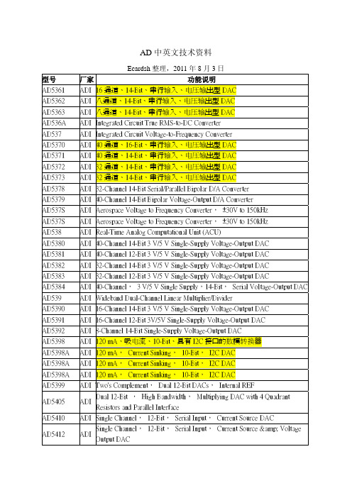
AD中英文技术资料Ecardsh整理,2011年8月3日型号厂家功能说明AD5361 ADI 16通道、14-Bit、串行输入、电压输出型DACAD5362 ADI 八通道、14-Bit、串行输入、电压输出型DACAD5363 ADI 八通道、14-Bit、串行输入、电压输出型DACAD536A ADI Integrated Circuit True RMS-to-DC ConverterAD537 ADI Integrated Circuit Voltage-to-Frequency ConverterAD5370 ADI 40通道、16-Bit、串行输入、电压输出型DACAD5371 ADI 40通道、14-Bit、串行输入、电压输出型DACAD5372 ADI 32通道、14-Bit、串行输入、电压输出型DACAD5373 ADI 32通道、14-Bit、串行输入、电压输出型DACAD5378 ADI 32-Channel 14-Bit Serial/Parallel Bipolar D/A ConverterAD5379 ADI 40-Channel 14-Bit Bipolar Voltage-Output D/A ConverterAD537S ADI Aerospace Voltage to Frequency Converter, ±30V to 150kHzAD537S ADI Aerospace Voltage to Frequency Converter, ±30V to 150kHzAD538 ADI Real-Time Analog Computational Unit (ACU)AD5380 ADI 40-Channel 14-Bit 3 V/5 V Single-Supply Voltage-Output DACAD5381 ADI 40-Channel 12-Bit 3 V/5 V Single-Supply Voltage-Output DACAD5382 ADI 32-Channel 14-Bit 3 V/5 V Single-Supply Voltage-Output DACAD5383 ADI 32-Channel 12-Bit 3 V/5 V Single-Supply Voltage-Output DACAD5384 ADI 40-Channel, 3 V/5 V Single Supply,14-Bit, Serial Voltage-Output DAC AD539 ADI Wideband Dual-Channel Linear Multiplier/DividerAD5390 ADI 16-Channel 14-Bit 3 V/5 V Single-Supply Voltage-Output DACAD5391 ADI 16-Channel 12-Bit 3V/5V Single-Supply Voltage-Output DACAD5392 ADI 8-Channel 14-Bit Single-Supply Voltage-Output DACAD5398 ADI 120 mA、吸电流、10-Bit、具有I2C接口的数模转换器AD5398A ADI 120 mA, Current Sinking, 10-Bit, I2C DACAD5398A ADI 120 mA, Current Sinking, 10-Bit, I2C DACAD5398A ADI 120 mA, Current Sinking, 10-Bit, I2C DACAD5399 ADI Two's Complement, Dual 12-Bit DACs, Internal REFAD5405 ADI Dual 12-Bit , High Bandwidth, Multiplying DAC with 4 Quadrant Resistors and Parallel InterfaceAD5410 ADI Single Channel, 12-Bit, Serial Input, Current Source DACAD5412 ADI Single Channel, 12-Bit, Serial Input, Current Source & Voltage Output DACAD5415 ADI Dual 12-Bit,High Bandwidth,Multiplying DAC with 4 Quadrant Resistors and Serial InterfaceAD5420 ADI Single Channel, 16-Bit, Serial Input, Current Source DACAD5422 ADI 单通道,16-Bit, 串行输入, 电流源与电压输出数模转换器AD5424 ADI High Bandwidth CMOS 8-Bit Parallel Interface Multiplying D/A Converter AD5425 ADI High Bandwidth, CMOS 8-Bit Serial Interface Multiplying D/A Converter AD5426 ADI High Bandwidth CMOS 8-Bit Serial Interface Multiplying D/A Converter AD5428 ADI Dual 8-Bit, High Bandwidth Multiplying DACs with Parallel InterfaceAD5429 ADI Dual 8-Bit, High Bandwidth Multiplying D/A Converter With Serial InterfaceAD5432 ADI High Bandwidth CMOS 10-Bit Serial Interface Multiplying D/A Converter AD5433 ADI High Bandwidth CMOS 10-Bit Parallel Interface Multiplying D/A ConverterAD5439 ADI Dual 10-Bit, High Bandwidth Multiplying D/A Converter With Serial InterfaceAD5440 ADI Dual 10-Bit, High Bandwidth Multiplying DACs with Parallel Interface AD5441 ADI 12-Bit串行输入乘法型数模转换器AD5441 ADI 12-Bit串行输入乘法型数模转换器AD5443 ADI High Bandwidth CMOS 12-Bit Serial Interface Multiplying D/A Converter AD5444 ADI 12-Bit High Bandwidth Multiplying DAC with Serial InterfaceAD5445 ADI High Bandwidth CMOS 12-Bit Parallel Interface Multiplying D/A Converter AD5446 ADI 14-Bit High Bandwidth Multiplying DAC with Serial InterfaceAD5447 ADI Dual 12-Bit, High Bandwidth Multiplying DACs with Parallel InterfaceAD5449 ADI Dual 12-Bit, High Bandwidth Multiplying D/A Converter With Serial InterfaceAD5450 ADI 8-Bit High Bandwidth Multiplying DACs with Serial InterfaceAD5451 ADI 10-Bit High Bandwidth Multiplying DACs with Serial InterfaceAD5452 ADI 12-Bit High Bandwidth Multiplying DACs with Serial InterfaceAD5453 ADI 14-Bit High Bandwidth Multiplying DACs with Serial InterfaceAD548 ADI Precision, Low Power BiFET Op AmpAD549 ADI Ultralow Input-Bias Current Operational AmplifierAD5516 ADI 16-Channel 12-Bit Bipolar Voltage-Output DAC with 14-Bit Increment Mode AD5520 ADI Per-pin Parametric Measurement Unit / Source Measure UnitAD5522 ADI 集成16位电平设置DAC的四参数测量单元AD5530 ADI Serial Input, Voltage Output 12-Bit D/A ConverterAD5531 ADI Serial Input, Voltage Output14-Bit D/A ConverterAD5532 ADI 32-Channel 14-Bit Bipolar Voltage-Output DACAD5532B ADI 32-Channel 14-bit Bipolar Voltage-Output DACAD5532HS ADI 32-Channel 14-Bit bipolar DAC with High Speed 3-Wire Serial Interface AD5533 ADI 32-Channel Infinite Sample-and-HoldAD5533B ADI 32-Channel Infinite Sample-and-HoldAD5535 ADI 32-Channel, 14-Bit DAC with Fullscale Output Voltage Programmable from 50 V to 200 VAD5541 ADI 16-Bit Voltage-Output DAC in SO-8 PackageAD5542 ADI 16-Bit Bipolar-Voltage-Output DAC with Kelvin SensingAD5543 ADI 16-Bit DAC in μSOIC-8 PackageAD5544 ADI Precision QUAD 16-Bit D/A ConverterAD5545 ADI Precision DUAL 16-Bit and 14-Bit DACs in Compact TSSOP Packages AD5546 ADI Current-Output Parallel-Input, 16-Bit Digital-to-Analog Converter AD5547 ADI Dual Current-Output Parallel-Input, 16-Bit DACAD5551 ADI 5 V, Serial-Input, Voltage-Output 14-Bit DACAD5552 ADI 5 V, Serial-Input, Voltage-Output 14-Bit DAC With Bipolar Output CapabilityAD5553 ADI 14-Bit DAC in μSOIC-8 PackageAD5554 ADI Precision QUAD 14-Bit D/A ConverterAD5555 ADI Precision DUAL 16-Bit 14-Bit-DACs in Compact TSSOP Packages AD5556 ADI Current-Output Parallel-Input, 14-Bit Digital-to-Analog Converter AD5557 ADI Dual Current-Output Parallel-Input, 14-Bit DACAD5560 ADI 1.2A Programmable Device Power Supply with Integrated 16-bit Level Setting DACsAD5560 ADI 1.2A Programmable Device Power Supply with Integrated 16-bit Level Setting DACsAD5564 ADI This product is obsolete and replaced by the AD5532. (9/99) AD557 ADI DACPORT Low Cost, Complete μP-Compatible 8-Bit DACAD5570 ADI True Accuracy, 16-Bit ±12 V/±15 V, Serial Input Voltage Output D/A ConverterAD558 ADI Voltage-output 8-bit digital-to-analog converter,including output amplifier,full microprocessor interface and precisionAD5582 ADI +15 V, Quad, Parallel Input, 12-Bit D/A Converter AD5583 ADI +15V, Quad, Parallel Input, 10-Bit D/A Converter AD5590 ADI 16输入/16输出模拟I/O端口,集成放大器AD5601 ADI 2.7 V to 5.5 V,<100 μA,8-Bit <em>nano</em>DAC?,SPI Interface in SC70 PackageAD5602 ADI 2.7 V to 5.5 V, <100 μA, 8-Bit <em>nano</em>DAC? D/A Converter with I2C Compatible Interface, Tiny SC70 PackageAD561 ADI Low Cost 10-Bit Monolithic D/A ConverterAD5611 ADI 2.7 V to 5.5 V,<100 μA,10-Bit <em>nano</em>DAC?,SPI Interface in SC70 PackageAD5612 ADI 2.7 V to 5.5 V,<100 μA,10-Bit <em>nano</em>DAC? D/A Converter with I2C Compatible Interface, Tiny SC70 PackageAD561S ADI Aerospace 10-Bit, Current Output DACAD5620 ADI 3 V/5 V, 12-Bit <em>nano</em>DAC? Converter with 5 ppm/°C On-Chip Reference in Sot-23AD5621 ADI 2.7 V to 5.5 V,<100 μA,12-Bit <em>nano</em>DAC?,SPI Interface in SC70 PackageAD5622 ADI 2.7 V to 5.5 V,<100 μA,12-Bit <em>nano</em>DAC? D/A Converter with I2C Compatible Interface, Tiny SC70 PackageAD5623R ADI Dual 12-Bit <em>nano</em>DAC? with 5 ppm/°C On-Chip ReferenceAD5624 ADI 2.7 V to 5.5 V, 450 μA, Rail-to-Rail Output, Quad, 12-/16-Bit <em>nano</em>DACs?AD5624R ADI Quad,12-Bit <em>nano</em>DAC? with 5ppm/°C On-Chip Reference AD5625 ADI Quad, 12-Bit <em>nano</em>DACs?, I2C? InterfaceAD5625R ADI Quad, 12-Bit <em>nano</em>DACs? with 5 ppm/°C On-Chip Reference,I2C? InterfaceAD5626 ADI 5 V,12-Bit <em>nano</em>DAC?,串行接口,采用MSOP与LFCSP 封装AD5627 ADI Dual, 12-Bit nanoDAC? with I2C? InterfaceAD5627R ADI Dual,12-Bit nanoDAC? with 5 ppm/°C On-Chip Reference,I2C? InterfaceAD5628 ADI Octal, 12-Bit D/A Converter with 5 ppm/°C On-Chip Reference in 14-Lead TSSOPAD563 ADI ObsoleteAD5640 ADI 3 V/5 V, 14-Bit <em>nano</em>DAC? Converter with 5 ppm/°C On-Chip Reference in Sot-23AD5641 ADI 2.7 V to 5.5 V,<100 μA,14-Bit <em>nano</em>DAC,SPI Interface in SC70 PackageAD5643R ADI Dual 14-Bit <em>nano</em>DAC? with 5 ppm/°C On-Chip Reference AD5644R ADI Quad, 14-Bit <em>nano</em>DAC? with 5ppm/°C On-Chip ReferenceAD5645R ADI Quad, 14-Bit <em>nano</em>DACs? with 5 ppm/°C On-Chip Reference,I2C? InterfaceAD5647R ADI Dual,14-Bit nanoDAC? with 5 ppm/°C On-Chip Reference,I2C? InterfaceAD5648 ADI Octal, 14-Bit D/A Converter with 5 ppm/°C On-Chip Reference in 14-Lead TSSOPAD565A ADI 12-bit Digital-to-Analog Converters, with Zener ReferenceAD565S ADI Aerospace 12-Bit, Current Output, Complete High Speed DACAD5660 ADI 3 V/5 V, 16-Bit <em>nano</em>DAC? Converter with 5 ppm/°C On-Chip Reference in a Sot-23AD5662 ADI 2.7-5.5V, 16-Bit <em>nano</em>DAC? Converter in a Sot-23AD5663 ADI 2.7 V to 5.5 V, 250 μA, Rail-to-Rail Output, Dual 16-Bit <em>nano</em>DAC?AD5663R ADI Dual 16-Bit <em>nano</em>DAC? with 5 ppm/°C On-Chip ReferenceAD5664 ADI 2.7 V to 5.5 V, 450 μA, Rail-to-Rail Output, Quad, 12-/16-Bit <em>nano</em>DACs?AD5664R ADI Quad, 16-Bit <em>nano</em>DAC? with 5ppm/°C On-Chip Reference AD5665 ADI Quad, 16-Bit <em>nano</em>DACs?, I2C? InterfaceAD5665R ADI 片上带5ppm/°C基准源和I2C接口的16bit 四nanoDAC?AD5666 ADI Quad, 16 Bit D/A Converter with 10ppm/°C Max On-Chip Reference in 14-Lead TSSOPAD5667 ADI Dual, 16-Bit nanoDAC? with I2C? InterfaceAD5667R ADI Dual,16-Bit nanoDAC? with 5 ppm/°C On-Chip Reference,I2C? InterfaceAD5668 ADI Octal, 16-Bit D/A Converter with 5 ppm/°C On-Chip Reference in 16-Lead TSSOPAD567 ADI 12-Bit Current Output, Microprocessor-Compatible DACAD5678 ADI 4 x 12-Bit and 4 × 16-Bit Octal D/A Converter with On-Chip Reference in 14-Lead TSSOPAD568 ADI 12-Bit Ultrahigh Speed Monolithic D/A ConverterAD5680 ADI 5 V 18-Bit <em>nano</em>DAC? in a SOT-23AD569 ADI 16-Bit Monotonic Voltage Output D/A ConverterAD570 ADI 8-Bit Successive Approximation Analog-to-Digital ConverterAD571 ADI 10-Bit, A/D Converter, Complete with Reference and Clock AD571S ADI Aerospace 10-Bit Complete Anolog to Digital ConverterAD572 ADI 12-Bit Successive Approximation Integrated Circuit A/D ConverterAD5722 ADI Complete,Dual,12-Bit,Serial Input,Unipolar/Bipolar,Voltage Output DACAD5722 ADI Complete,Dual,12-Bit,Serial Input,Unipolar/Bipolar,Voltage Output DACAD5722R ADI Complete,Dual,12-Bit,Serial Input,Unipolar/Bipolar,Voltage Output DACAD5724 ADI Complete,Quad,12-Bit,Serial Input,Unipolar/Bipolar Voltage Output DACsAD5724 ADI Complete,Quad,12-Bit,Serial Input,Unipolar/Bipolar Voltage Output DACsAD5724R ADI Complete,Quad,12-Bit,Serial Input,Unipolar/Bipolar Voltage OutputDACAD5725 ADI 12-bit、并行输入、单极性/双极性、电压输出四DACAD5726 ADI Quad, 12-Bit, Serial Input, Unipolar/Bipolar, Voltage Output DAC AD573 ADI 10-bit successive approximation ADC.AD5732 ADI Complete,Dual,14-Bit,Serial Input,Unipolar/Bipolar,Voltage Output DACAD5732 ADI Complete,Dual,14-Bit,Serial Input,Unipolar/Bipolar,Voltage Output DACAD5732R ADI Complete,Dual,14-Bit,Serial Input,Unipolar/Bipolar,Voltage Output DACAD5734 ADI Complete,Quad,14-Bit,Serial Input,Unipolar/Bipolar Voltage Output DACAD5734 ADI Complete,Quad,14-Bit,Serial Input,Unipolar/Bipolar Voltage Output DACAD5734R ADI Complete,Quad,14-Bit,Serial Input,Unipolar/Bipolar Voltage Output DACAD5744 ADI Complete,Quad,14-Bit,High Accuracy,Serial Input,Bipolar Voltage Output D/A ConverterAD5744R ADI Complete Quad, 14-Bit, High Accuracy, Serial Input, Bipolar Voltage Output D/A ConverterAD5744R ADI Complete Quad, 14-Bit, High Accuracy, Serial Input, Bipolar Voltage Output D/A ConverterAD574A ADI Complete 12-Bit A/D ConverterAD574S ADI Aerospace 12-Bit-ADC w/Microprocessor InterfaceAD575 ADI ObsoleteAD5750 ADI AD5750 电流/电压输出驱动器,输出范围可编程,适合工业应用 AD5750 ADI AD5750 电流/电压输出驱动器,输出范围可编程,适合工业应用AD5751 ADI 电流/电压输出驱动器,单电源供电,60 V电压范围,输出范围可编程,适合工业应用AD5751 ADI 电流/电压输出驱动器,单电源供电,60 V电压范围,输出范围可编程,适合工业应用AD5752 ADI Complete,Dual,16-Bit,Serial Input,Unipolar/Bipolar,Voltage Output DACAD5752 ADI Complete,Dual,16-Bit,Serial Input,Unipolar/Bipolar,Voltage Output DACAD5752R ADI Complete,Dual,16-Bit,Serial Input,Unipolar/Bipolar,Voltage Output DACAD5754 ADI 完全4通道、16 Bit、串行输入、单极/双极性电压输出数模转换器AD5754R ADI Complete,Quad,16-Bit,Serial Input,Unipolar/Bipolar Voltage Output DACAD5762R ADI 16-Bit,双通道,高精度, 串行输入, 双极性电压输出型DAC AD5763 ADI Complete Dual, 16-Bit, High Accuracy, Serial Input, ±5V DACsAD5764 ADI Complete Quad, 16-Bit, High Accuracy, Serial Input, Bipolar Voltage Output DACsAD5764R ADI Complete Quad, 16-Bit, High Accuracy, Serial Input, Bipolar Voltage Output D/A ConverterAD5764R ADI Complete Quad, 16-Bit, High Accuracy, Serial Input, Bipolar Voltage Output D/A ConverterAD5765 ADI Complete Quad, 16-Bit, High Accuracy, Serial Input, ±5V DACs AD580 ADI High Precision 2.5 V IC ReferenceAD581 ADI High Precision 10 V IC ReferenceAD582 ADI Low-Cost Sample-and-Hold AmplifierAD5821 ADI 120 mA, Current Sinking, 10-Bit, I2C? DACAD5821A ADI 120 mA, Current Sinking, 10-Bit, I2C DACAD5821A ADI 120 mA, Current Sinking, 10-Bit, I2C DACAD5821A ADI 120 mA, Current Sinking, 10-Bit, I2C DACAD583 ADI ObsoleteAD584 ADI Pin Programmable Precision Voltage ReferenceAD584S ADI Aerospace Pin Programmable Precision Voltage ReferenceAD585 ADI Complete Monolithic SHA Circuit.AD585S ADI Aerospace High Speed, Precision Sample-and-Hold AmplifierAD586 ADI High Precision 5 V ReferenceAD587 ADI High Precision 10 V ReferenceAD588 ADI High Precision Voltage ReferenceAD589 ADI Two-Terminal IC 1.2 V ReferenceAD589S ADI Aerospace Precision 1.2 Volt IC ReferenceAD590 ADI Two Terminal IC Temperature TransducerAD590S ADI Aerospace 2 Terminal Temperature Transducer, 1uA/°KAD592 ADI Current Output – Precision IC Temperature TransducerAD5930 ADI Programmable Frequency Sweep and Output Burst Waveform Generator AD5932 ADI 可编程单扫描波形发生器AD5933 ADI 1 MSPS,12 bit阻抗转换器和网络分析器AD5934 ADI 250 kSPS 12-Bit Impedance Converter Network AnalyzerAD594 ADI Monolithic Thermocouple Amplifier with Cold Junction Compensation Pretrimmed for Type J ThermocouplesAD595 ADI Monolithic Thermocouple Amplifier with Cold Junction Compensation Pretrimmed for Type K ThermocouplesAD596 ADI Thermocouple Conditioner and Setpoint Controller Operates with Type J ThermocoupleAD597 ADI Thermocouple Conditioner and Setpoint Controller Operates with Type K ThermocoupleAD598 ADI LVDT Signal ConditionerAD600 ADI Dual, Low Noise, Wideband Variable Gain Amplifier, 0 dB To +40 dB GainAD602 ADI Dual,Low Noise,Wideband Variable Gain Amplifier,-10 dB To +30 dB GainAD6021 ADI Othello One ET? Quad Band EDGE Transmit ModulatorAD603 ADI Low Noise, 90 MHz Variable Gain AmplifierAD604 ADI Dual, Ultralow Noise Variable Gain AmplifierAD605 ADI Dual, Low Noise, Single-Supply Variable Gain AmplifierAD606 ADI 50 MHz, 80 dB Demodulating Logarithmic Amplifier with Limiter Output AD607 ADI Low Power Mixer/AGC/RSSI 3V Receiver IF SubsystemAD608 ADI Low Power Mixer/Limiter/RSSI 3 V Receiver IF SubsystemAD620 ADI Low Drift, Low Power Instrumentation Amp with Set Gains of 1 to 10000 AD621 ADI Low Drift, Low Power Instrumentation Amp with fixed gains of 10 and 100 AD622 ADI 低成本仪表放大器AD623 ADI Single Supply, Rail-Rail, Low Cost Instrumentation AmplifierAD624 ADI High Precision, Low Noise Instrumentation AmplifierAD625 ADI Programmable Gain Instrumentation AmplifierAD626 ADI Low Cost, Single-Supply Differential AmplifierAD627 ADI 微功耗,单电源/双电源,轨到轨仪表放大器AD628 ADI High Common-Mode Voltage, Programmable Gain Difference Amplifier AD629 ADI High Common-Mode Voltage, Difference AmplifierAD630 ADI Balanced Modulator/DemodulatorAD632 ADI Internally Trimmed Precision IC MultiplierAD633 ADI Low Cost Four-Quadrant Analog MultiplierAD636 ADI Low Level, True RMS-to-DC ConverterAD637 ADI High Precision, Wideband RMS-to-DC ConverterAD640 ADI 120 MHz, 50 dB Demodulating Logarithmic AmplifierAD641 ADI 250 MHz, 44 dB Demodulating Logarithmic AmplifierAD6411 ADI DECT RF TransceiverAD648 ADI Dual Precision, Low Power BiFET Op AmpAD6488 ADI ADSL2+ CPE Analog Front EndAD648S ADI Aerospace Dual Precision, Low Power BiFET Op AmpAD650 ADI Voltage-to-Frequency and Frequency-to-Voltage ConverterAD651 ADI ObsoleteAD652 ADI Monolithic Synchronous Voltage-to-Frequency ConverterAD6524 ADI GSM Multi-Band SynthesizerAD6534 ADI Othello One Single-Chip Direct-Conversion GSM/GPRS/EDGE RFICAD6538 ADI Othello One Plus? Direct Conversion GSM/GPRS/EDGE Transceiver with Integrated LO VCOAD6539 ADI Othello One TV? Single Chip Direct Conversion GSM/GPRS Transceiver with Integrated TX VCOsAD654 ADI Low Cost Monolithic Voltage-to-Frequency ConverterAD660 ADI Monolithic 16-Bit Serial/Byte DACPORTAD6600 ADI Diversity Receiver ChipsetAD6620 ADI 65MSPS Digital Receive Signal ProcessorAD6622 ADI 65 MSPS, Quad Transmit Signal Processor (TSP)AD6623 ADI 104 MSPS, Four-Channel Digital Transmit Signal Processor (TSP) AD6624 ADI 80 MSPS, Quad Receiver Signal ProcessorAD6624A ADI Four-Channel, 100 MSPS Digital Receive Signal Processor (RSP) AD6630 ADI Differential, Low Noise IF Gain Block with Output ClampingAD6633 ADI Multi-channel (Digital) Transmit Signal Processor (TSP) with VersaCREST? Crest Reduction EngineAD6634 ADI 80 MSPS, Dual-Channel, WCDMA Receive Signal Processor (RSP) AD6635 ADI Four-Channel, 80 MSPS WCDMA Receive Signal Processor (RSP) AD6636 ADI 150 MSPS Wideband (Digital) Receive Signal Processor (RSP)AD664 ADI Monolithic 12-Bit Quad DACAD6640 ADI Multi-Channel, Multi-Mode Receiver ChipsetAD6644 ADI 14-Bit, 40 MSPS/65 MSPS Analog-to-Digital ConverterAD6645 ADI 14-Bit, 80 MSPS/105 MSPS A/D ConverterAD6645-MILADI 14-Bit, 80 MSPS Analog to Digital ConverterAD6650 ADI Diversity IF-to-Baseband GSM/EDGE Narrow-Band ReceiverAD6652 ADI 12-Bit, 65 MSPS IF to Base Band Diversity ReceiverAD6653 ADI IF Diversity ReceiverAD6654 ADI 14-Bit, 92.16 MSPS, 4 & 6-Channel Wideband IF to Base Band ReceiverAD6655 ADI IF Diversity ReceiverAD667 ADI Microprocessor-Compatible 12-Bit D/A ConverterAD667S ADI Aerospace 12-Bit Microprocessor Compatible DACAD668 ADI 12-Bit Ultrahigh Speed Multiplying D/A ConverterAD669 ADI Monolithic 16-Bit DACPORTAD670 ADI 8-Bit Signal Conditioning ADC.AD670S ADI Aerospace 8-Bit Low Cost Signal Conditioning Single Supply AD673 ADI 8-bit Successive Approximation, ADCAD674B ADI Complete 12-Bit A/D ConvertersAD676 ADI 16-Bit Parallel 100 kSPS Sampling ADCAD677 ADI 16-Bit, Serial, 100 kSPS Sampling ADC.AD678 ADI 12-Bit 200 kSPS Complete Sampling ADCAD679 ADI 14-Bit 128 kSPS Complete Sampling ADCAD680 ADI Bandgap, Low Power 2.5v ReferenceAD682 ADI ObsoleteAD684 ADI Monolithic Quad Sample-and-hold Amplifier (SHA)AD688 ADI High Precision ±10 V ReferenceAD689 ADI ObsoleteAD693 ADI Loop-Powered 4-20 mA Sensor TransmitterAD694 ADI 4-20mA Monolithic Current TransmitterAD698 ADI Universal LVDT Signal ConditionerAD7011 ADI CMOS, ADC pi/4 DQPSK Baseband Transmit PortAD704 ADI Quad Picoampere Input Current Bipolar Op AmpAD706 ADI Dual Picoampere Input Current Bipolar Op AmpAD708 ADI Ultralow Offset Voltage Dual Op AmpAD71028 ADI Dual Digital BTSC Encoder with Integrated DACAD711 ADI Precision, Low Cost, High Speed, BiFET Op Amp AD7111 ADI Monolithic Multiplying DAC Featuring Wide Dynamic RangeAD7112 ADI Dual CMOS Multiplying DAC with Anti-Log Transfer Function for Audio Volume Control ApplicationsAD712 ADI Dual Precision, Low Cost, High Speed, BiFET Op Amp AD713 ADI Quad Precision, Low Cost, High Speed, BiFET Op Amp AD7142 ADI 电容式触摸传感器专用可编程控制器AD7143 ADI 电容式触摸传感器专用可编程控制器AD7147 ADI CapTouch?单电极电容式传感器专用可编程控制器AD7148 ADI AD7148 可编程触摸控制器,用于单电极电容传感器AD7150 ADI 用于近程传感的超低功耗双通道电容式转换器。
测速雷达主要设备功能及技术参数

测速雷达主要设备功能及技术参数测速雷达型号:KTR-C3(品牌:KITOZER/开拓者)采用高速DSP信号处理芯片、0.1秒快速捕捉。
1)设计小巧轻便、制作精良。
2)纯铸铁结构,坚固耐用。
3)232串口输出。
4)精确度高,捕捉目标速度快。
5)动态时具有同向功能。
6)静态时可分别检测来车、去车。
7)静态测速范围:0~322 KPH。
8)移动测速范围:19~322KPH。
9)环境要求:温度:-30度 ~ +70度;湿度:0 % ~ 90% 。
10)Ka波段窄波雷达,微波频率:34.7GHz(Ka-band),可有效规避探测狗检测。
11)发射角:±4度。
12)规格:重:0.52kg、直径:6.7cm、长:11.8cm。
13)精确度:+/-1KPH。
高清摄像机(品牌:KITOZER/开拓者)高清摄像机功能:CCD成像,200万象素,主要端口有:闪光灯同步口,通过同步线与闪光灯连接;拍照触发口,当收到外部脉冲触发信号时,高清摄像机会抓取一张图片,脉冲信号由独立的拍照触发器发出;网口(100M),与控制主机连接,接收参数配置,上传图片,也可接收带由协议内容的抓拍命令。
产品详细参数表百万像素变焦镜头日本精工本次中煤平朔公司系统百万像素变焦镜头选型为日本精工SE5018MP产品,AVENIR ETOKU(日本精工)十几年来始终专心于监控镜头的市场发展,成为中国安防监控领域用得最多的专业镜头。
本次系统高清摄像机选型为广州莱安智能化系统开发有限公司出品的KTR200A型高清摄像机。
KTR200A是集成一体的高速彩色/单色智能工业相机,采用总像素200万像素的CCD图像传感器,具有处理速度快、分辨率高、图像质量好等特点。
广泛应用于智能交通、电子警察、卡口、高速公路、停车厂等领域的检测和识别。
百万像素网络拍照摄像一体机,将高清图像抓拍、标清视频摄像完美结合,超高清晰度,分辨率达130万~500万像素,专业用于如平安城市建设、机场、银行、道路卡口监控及牌照识别等安全防范领域,能够为客户提供专业的可定制产品及服务,支持后续增值开发。
无线红外防盗报警器的设计

1 前言随着微电子技术与网络技术的飞速进展,人们关于居住环境的平安、方便、舒适提出了愈来愈高的要求因此智能化住宅就随之显现,也随着改革开放的深切和市场经济的迅速进展、提高,城市外来流动人口的大量增加,带来了许多不平安因素,刑事案件专门是入室盗窃、抢劫居高不下,因此家庭智能平安防范系统是智能化小区建设中不可缺少的一项,而以往的做法是安装防盗门、防盗网,但普遍存在有碍美观,不符合防火要求,而且不能有效地避免犯法分子对住宅的入侵,故利用高科技的电子防盗报警系统也就应运而生。
无线红外防盗报警器的进展主若是基于传感器之上,因此有必要先谈谈红别传感器的进展状况。
而传感器技术是21世纪人们在高新技术进展方面争夺的一个制高点,各发达国家都将传感技术视为现代高新技术进展的关键。
从20世纪80年代起,日本就将传感器技术列为优先进展的高新科技之首,美国等西方国家也将此技术列为国家科技和国防技术进展的重点。
从而基于传感器技术的防盗报警系统也取得了高速进展。
不管是基于哪一种方式的无线防盗报警器,它的工作原理都是将探测到的信号,通过编码,经电路放大,输出并将报警信号通过天线发射出,再用接收电路接收信号,解码并通过操纵电路判定是不是属于异样信号,再决定是不是发送报警信号给报警电路,从而达到防盗的成效,本系统也是采纳此原理。
本系统采纳经常使用的STC89C52单片机作为系统的核心操纵部份,是一个利用红别传感器作为信号输入的操纵部份的智能报警器。
当有不明人物进过红外探头时,会有操纵信号输入单片机,进而输出扎耳报警声引发相关人员的注意,同时利用显示器来显示。
如此专门大程度上减少了搜索时刻,从而提高了时效性。
达到了信号同意灵明度高,显示反映快,报警声音响的成效。
2 整体方案设计方案比较2.1.1 方案一图方案一方框图2.1.1 方案二图方案二方框图方案论证2.3.1 收发模块的比较方案一中收发模块采纳的核心芯片是Nrf905,此芯片为32引脚芯片,工作电压在,需外接433MHz 50Ω天线。
AD9235中文资料
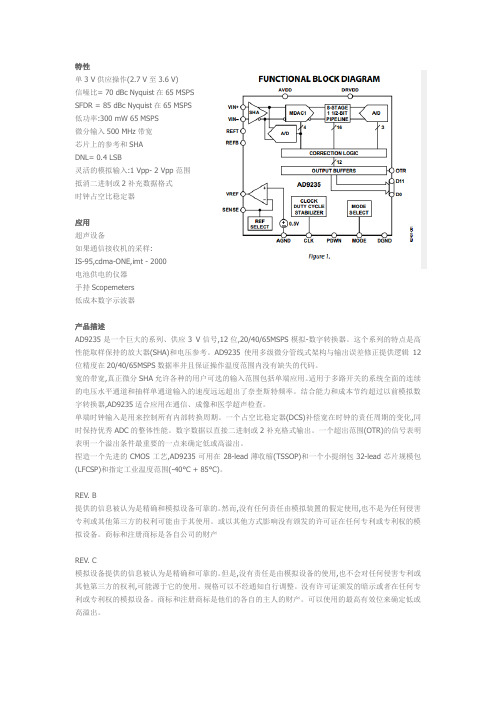
特性单3 V供应操作(2.7 V至3.6 V)信噪比= 70 dBc Nyquist在65MSPSSFDR = 85 dBc Nyquist在65MSPS低功率:300 mW 65MSPS微分输入500 MHz带宽芯片上的参考和SHADNL= 0.4 LSB灵活的模拟输入:1 Vpp- 2 Vpp范围抵消二进制或2补充数据格式时钟占空比稳定器应用超声设备如果通信接收机的采样:IS-95,cdma-ONE,imt - 2000电池供电的仪器手持Scopemeters低成本数字示波器产品描述AD9235是一个巨大的系列、供应3 V信号,12位,20/40/65MSPS模拟-数字转换器。
这个系列的特点是高性能取样保持的放大器(SHA)和电压参考。
AD9235使用多级微分管线式架构与输出误差修正提供逻辑12位精度在20/40/65MSPS数据率并且保证操作温度范围内没有缺失的代码。
宽的带宽,真正微分SHA允许各种的用户可选的输入范围包括单端应用。
适用于多路开关的系统全面的连续的电压水平通道和抽样单通道输入的速度远远超出了奈奎斯特频率。
结合能力和成本节约超过以前模拟数字转换器,AD9235适合应用在通信、成像和医学超声检查。
单端时钟输入是用来控制所有内部转换周期。
一个占空比稳定器(DCS)补偿宽在时钟的责任周期的变化,同时保持优秀ADC的整体性能。
数字数据以直接二进制或2补充格式输出。
一个超出范围(OTR)的信号表明表明一个溢出条件最重要的一点来确定低或高溢出。
捏造一个先进的CMOS工艺,AD9235可用在28-lead薄收缩(TSSOP)和一个小提纲包32-lead芯片规模包(LFCSP)和指定工业温度范围(-40°C + 85°C)。
REV. B提供的信息被认为是精确和模拟设备可靠的。
然而,没有任何责任由模拟装置的假定使用,也不是为任何侵害专利或其他第三方的权利可能由于其使用。
或以其他方式影响没有颁发的许可证在任何专利或专利权的模拟设备。
AD404M326VQA-5中文资料
ASCEND Semiconductor 4Mx4 EDO Data sheetDescriptionThe device CMOS Dynamic RAM organized as 4,194,304 words x 4 bits with extended data out access mode. It is fabricated with an advanced submicron CMOS technology and designed to operate from a single 3.3V oniy power supply. Low voltage operation is more suitable to be used on battery backup, portable elec-tronic application. lt is packaged in JEDEC standard 26/24-pin plastic SOJ or TSOP(II).Features• Single 3.3V(%) only power supply • High speed t RAC acess time: 50/60ns • Low power dissipation- Active mode : 432/396 mW (Mas) - Standby mode: 0.54 mW (Mas)• Extended - data - out(EDO) page mode access • I/O level: CMOS level (Vcc = 3.3V)• 2048 refresh cycle in 32 ms(Std.) or 128 ms(S-version)• 4 refresh modesh: - RAS only refresh- CAS - before - RAS refresh - Hidden refresh - Self-refresh(S-version)10±Pin Name FunctionA0-A10Address inputs- Row address - Column address - Refresh address DQ1~DQ4Data-in / data-out RAS Row address strobe CAS Column address strobe WE Write enable OE Output enable Vcc Power (+ 3.3V)VssGroundVCC 1DQ12DQ23DQ34DQ45VCC6891011 NC 12 WE 13A0 A117 A218 A319VSS RAS CAS OE A8A7A6A5A4VSSAD404M42VSPin Description Pin Configuration21222324 2526151416 A1026/24-PIN 300mil Plastic SOJA9VCC 1DQ12DQ23DQ34DQ45VCC6891011 NC 12 WE 13A0 A117 A218 A319VSS RAS CAS OE A8A7 A6A5 A4VSSAD404M42VT212223242526151416 A1026/24-PIN 300mil Plastic TSOP (ll)A9A0-A10A0-A10A0-A10WECASNO. 2 CLOCK GENERATORCOLUMN ADDRESS BUFFERS (11)REFRESH CONTROLLERREFRESH COUNTERBUFFERS (11)ADDRESS ROW NO. 1 CLOCK GENERATORA0RASA1A2A3A4A5A6A7A8CONTROLLOGICDATA-IN BUFFERDATA-OUT BUFFEROEDQ1.DQ4.COLUMN DECODER2048SENSE AMPLIFIERSI/O GATING2048x42048x2048x4MEMORY ARRAY2048R O W D E C O D E RVcc VssBlock DiagramA9A10TRUTH TABLENotes: 1. EARLY WRITE only.FUNCTIONRASCAS WE OE ADDRESSESDQ SNotesROW COL STANDBY H X X X X High-Z READL L H L ROW COL Data-Out WRITE: (EARLY WRITE )L L L X ROW COL Data-lnREAD WRITE L L ROW COL Data-Out,Data-ln EDO-PAGE-MODE READ1st Cycle L H L ROW COL Data-Out 2nd CycleL H L n/a COL Data-Out EDO-PAGE MODE WRITE1st CycleL L X ROW COL Data-In 2nd Cycle L L Xn/a COL Data-InEDO-PAGE-MODEREAD-WRITE 1st Cycle L ROW COL Data-Out, Data-In 2nd Cycle L n/a COL Data-Out, Data-In HIDDEN REFRESHREAD L H L ROW COL Data-Out WRITEL L X ROW COL Data-In 1RAS-ONLY REFRESH L H X X ROW n/a High-Z CBR REFRESHLHXXXHigh-ZH X →H L →L H →H L →H L →H L →H L →H L →H L →L H →H L →H L →L H→L H L →→L H L→→H L→Absolute Maximum RatingsRecommended DC Operating ConditionsCapacitanceTa = 25°C, V CC = 3.3V%, f = 1MHz Note: 1. Capacitance measured with effective capacitance measuring method. 2. RAS, CAS = V IH to disable Dout.ParameterSymbol Value Unit Voltage on any pin relative to Vss V T -0.5 to + 4.6V Supply voltage relative to Vss V CC -0.5 to + 4.6V Short circuit output current I OUT 50mA Power dissipation P D 1.0WOperating temperature T OPT 0 to + 70°C Storage temperatureT STG-55 to + 125°CParameter/Condition Symbol3.3 Volt VersionUnitMinTyp MaxSupply VoltageV CC 3.0 3.33.6V Input High Voltage, all inputs V IH 2.0-V CC + 0.3V Input Low Voltage, all inputsV IL-0.3-0.8VParameterSymbol Typ Max Unit Note Input capacitance (Address)C I1 -5pF 1Input capacitance (RAS, CAS, OE, WE)C I2-7pF 1Output capacitance(Data-in, Data-out)C I/O-7pF1, 210±DC Characteristics :(T a = 0 to 70°C, V CC = + 3.3V%, V SS = 0V)Parameter Symbol Test Conditions AD404M42V Unit Notes-5-6Min Max Min MaxOperating current I CC1RAS cyclingCAS, cyclingt RC = min-120-110mA1, 2Standby Current LowpowerS-versionI CC2LVTTL interfaceRAS, CAS = V IHDout = High-Z-0.5-0.5mACMOS interfaceRAS, -0.2VDout = High-Z-0.15-0.15mAStandardpowerversionLVTTL interfaceRAS, CAS = V IHDout = High-Z-2-2mACMOS interfaceRAS,-0.2VDout = High-Z-0.5-0.5mARAS- only refresh current I CC3RAS cycling, CAS = V IHt RC = min-120-110mA1, 2 EDO page mode current I CC4t PC = min-90-80mA1, 3CAS- before- RAS refresh current I CC5t RC = minRAS, CAS cycling-120-110mA1, 2Self- refresh current (S-Version)I CC8 - 550 - 55010±CAS V CC≥CAS V CC≥t RASS100µs≥µADC Characteristics :(T a = 0 to 70°C , V CC = +3.3V %, V SS = 0V)Notes:1. I CC is specified as an average current. It depends on output loading condition and cycle rate when the device is selected. I CC max is specified at the output open condition.2. Address can be changed once or less while RAS = V IL .3. For I CC4, address can be changed once or less within one EDO page mode cycle time.Parameter Symbol Test Conditions AD404M42VUnitNotes-5-6Min MaxMin MaxInput leakage current I LI + 0.3V -55-55Output leakage current I LO + 0.3V Dout = Disable -55-55Output high Voltage V OH I OH = -2mA 2.4- 2.4-V Output low voltage V OLI OL = +2mA-0.4-0.4V10±0V Vin V CC ≤≤µA 0V Vout V CC ≤≤µAAC Characteristics(T a = 0 to + 70°C , V cc = 3.3V %, V ss = 0V) *1, *2, *3, *4Test conditions• Output load: one TTL Load and 100pF (V CC = 3.3V %)• Input timing reference levels:V IH = 2.0V, V IL = 0.8V (V CC = 3.3V %)• Output timing reference levels:V OH = 2.0V, V OL = 0.8V10±10±10±Read, Write, Read- Modify- Write and Refresh Cycles (Common Parameters)ParameterSymbol AD404M42V UnitNotes-5-6Min MaxMin MaxRandom read or write cycle time t RC 84-104-ns RAS precharge timet RP 30-40-ns CAS precharge time in normal mode t CPN 10-10-ns RAS pulse width t RAS 50100006010000ns 5CAS pulse width t CAS 8100001010000ns 6Row address setup time t ASR 0-0-ns Row address hold time t RAH 8-10-ns Column address setup time t ASC 0-0-ns 7Column address hold time t CAH 8-10-ns RAS to CAS delay timet RCD 12371445ns 8RAS to column address delay time t RAD 10251230ns 9Column address to RAS lead time t RAL 25-30-ns RAS hold time t RSH 8-10-ns CAS hold timet CSH 38-40-ns CAS to RAS precharge time t CRP 5-5-ns 10OE to Din delay time t OED 12-15-ns Transition time (rise and fall)t T 150150ns 11Refresh periodt REF -32-32ms Refresh period (S- Version)t REF -128-128ms CAS to output in Low- Z t CLZ 0-0-ns CAS delay time from Din t DZC 0-0-ns OE delay time from Dint DZO-0-nsRead CycleWrite Cycle Parameter SymbolAD404M42V Unit Notes-5-6Min Max Min MaxAccess time from RAS t RAC-50-60ns12 Access time from CAS t CAC-14-15ns13, 14 Access time from column address t AA-25-30ns14, 15 Access time from OE t OEA-12-15nsRead command setup time t RCS0-0-ns7 Read command hold time to CAS t RCH0-0-ns10, 16 Read command hold time to RAS t RRH0-0-ns16 Output buffer turn-off time t OFF012015ns17 Output buffer turn-off time from OE t OEZ012015ns17Parameter SymbolAD404M42V Unit Notes -5-6Min Max Min MaxWrite command setup time t WCS0-0-ns7, 18 Write command hold time t WCH8-10-nsWrite command pulse width t WP8-10-nsWrite command to RAS lead time t RWL13-15-nsWrite command to CAS lead time t CWL8-10-nsData-in setup time t DS0-0-ns19 Data-in hold time t DH8-10-ns19 WE to Data-in delay t WED10-10-nsRead- Modify- Write CycleRefresh Cycle Parameter SymbolAD404M42V Unit Notes-5-6Min Max Min MaxRead-modify- write cycle time t RWC108-133-nsRAS to WE delay time t RWD64-77-ns18 CAS to WE dealy time t CWD26-32-ns18 Column address to WE delay time t AWD39-47-ns18 OE hold time from WE t OEH8-10-nsParameter SymbolAD404M42VUnit Notes -5-6Min Max Min MaxCAS setup time (CBR refresh) t CSR5-5-nsCAS hold time (CBR refresh)t CHR8-10-ns10 RAS precharge to CAS hold time t RPC5-5-ns7 RAS pulse width (self refresh)t RASS100-100-RAS precharge time (self refresh)t RPS90-110-nsCAS hold time (CBR self refresh)t CHS-50--50-nsWE setup time t WSR0-0-nsWE hold time t WHR10-10-nsµsEDO Page Mode CycleEDO Page Mode Read Modify Write CycleParameterSymbol AD404M42VUnit Notes-5-6Min MaxMin MaxEDO page mode cycle timet PC 20-25-ns EDO page mode CAS precharge time t CP 10-10-ns EDO page mode RAS pulse width t RASP 5010560105ns 20Access time from CAS precharge t CPA -30-35ns 10, 14RAS hold time from CAS precharge t CPRH 30-35-ns OE high hold time from CAS high t OEHC 5-5-ns OE high pulse widtht OEP 10-10-ns Data output hold time after CAS low t COH 5-5-ns Output disable delay from WEt WHZ 310310ns WE pulse width for output disable whenCAS hight WPZ7-7-nsParameterSymbol AD404M42V Unit Notes -5-6Min MaxMin MaxEDO page mode read- modify- write cycle CAS precharge to WE delay timet CPW 45-55-ns 10EDO page mode read- modify- write cycle timet PRWC56-68-nsNotes :1. AC measurements assume t T = 2ns.2. An initial pause of 100 is required after power up, and it followed by a minimum of eightinitialization cycles (RAS - only refresh cycle or CAS - before - RAS refresh cycle). If the internal refresh counter is used, a minimun of eight CAS - before - RAS refresh cycles are required.3. In delayed write or read-modify-write cycles, OE must disable output buffer prior to applying data to the device.4. All the V CC and V SS pins shall be supplied with the same voltages.5. t RAS (min) = t RWD (min)+t RWL (min)+t T in read-modify-write cycle.6. t CAS (min) = t CWD (min)+t CWL (min)+t T in read-modify-write cycle.7. t ASC (min), t RCS (min), t WCS (min), and t RPC are determined by the falling edge of CAS .8. t RCD (max) is specified as a reference point only, and t RAC (max) can be met with the t RCD (max) limit.Otherwise, t RAC is controlled exclusively by t CAC if t RCD is greater than the specified t RCD (max) limit. 9. t RAD (max) is specified as a reference point only, and t RAC (max) can be met with the t RAD (max) limit.Otherwise, t RAC is controlled exclusively by t AA if t RAD is greater than the specified t RAD (max) limit. 10. t CRP , t CHR , t RCH , t CPA and t CPW are determined by the rising edge of CAS .11. V IH (min) and V IL (max) are reference levels for measuring timing or input signals. Therefore, transitiontime is measured between V IH and V IL .12. Assumes that t RCD tRCD (max) and t RAD t RAD (max). If t RCD or t RAD is greater than the maximum recommended value shown in this table, t RAC exceeds the value shown. 13. Assumes that (max) and (max).14. Access time is determined by the maximum of t AA , t CAC , t CPA . 15. Assumes that (max) and (max). 16. Either t RCH or t RRH must be satisfied for a read cycle.17. t OFF (max) and t OEZ (max) define the time at which the output achieves the open circuit condition (highimpedance). t OFF is determined by the later rising edge of RAS or CAS.18. t WCS , t RWD , t CWD , and t AWD are not restrictive operating parameters. They are included in the datasheet as electrical characteristics only. If (min), the cycle is an early write cycle and the data out will remain open circuit (high impedance) throughout the entire cycle. If (min),(min), (min) and (min), the cycle is a read-modify-write and the data output will contain data read from the selected cell. If neither of the above sets of conditions is satisfied, the condition of the data output (at access time) is indeterminate.19. These parameters are referenced to CAS separately in an early write cycle and to WE edge in adelayed write or a read-modify-write cycle.20. t RASP defines RAS pulse width in EDO page mode cycles.µs ≤≤t RCD t RCD ≥t RADt RAD ≤t RCD t RCD ≤t RAD t RAD ≥t WCS t WCS ≥t RWD t RWD ≥t CWDt CWD ≥t AWD t AWD ≥t CPW t CPW≥Timing Waveforms• Read Cyclet RC t RASt RPtCRPtCPNtRRHtRCHt OEZ t OFF tOEA tCACt AAtRACt CLZD OUTtRCS t ASR tRAH tASC tCAH tRAD t RALtCAStRSH tRCDt TtCSHRASCASADDRESSWEDQ1~DQ4Note : = don’t care OEt OFFRowColumn= Invalid Dout•Early Write CycletRC t RASt RPt WCHt DSt DHt WCS t RALtCAStRSH tRCDt TtCSHRASCASWEDQ1~DQ4tCRPtASRtRAH tASCtCAH ADDRESSColumnRowtCPND INtRADt RAL• Delayed Write CycletRC t RASt RPt RWL t RCSt CAStRSH tRCDt TtCSHRASCAStASR tRAH tCAHADDRESSColumnRow tASC D INDQ1~DQ4WEtCRPtCPNt DHt DSt OEHt OEDOEt DSOPENt WPt CWL• Read - Modify - Write CycletRWC t RASt RPtRWDt WPtRADtRWL tCAStCWL tRCDt TtCPNRASCASWEtCRP t ASRtRAHtASCtCAHADDRESS Column RowDQ1~DQ4t DHt DSOEtRCStAWD tCWD D INt OEDt OEHt OEZt OEA t CAC t RACt AADQ1~DQ4D OUTOPENtDZCtDZO• EDO Page Mode Read CycletRASPtCPRHt RCStCAStRSH tRCDt OEAtCSHRASCAStASRtRAHtCAHADDRESStCASWEtCRPt CPOEDQ1~DQ4OPENtOEPD OUT 1t PCt CPtCAStCPNtCRPtRADtCAHtASCt ASCtCAHt ASCt RAL Row Column 1t OEAt OEHCtRRH tRCHt RACt AAt AAt AA t CPA t CPA t OEZt OFFt OFFt CACt OEZt CAC t CACt COHD OUT NWE OE Column 2Column N Rowt RPD OUT 2• EDO Page Mode Early Write CycletRASPtRPt WCSt CAStRSH tRCDRASCAStASRtRAHtCAHADDRESStCASWEt CPDQ1~DQ4t PCt CPt CAStCPNtCRP tCAH tASCtASC tCAH tASC Row Column 1t DS WE Column 2Column Nt WCH t WCS t WCH t WCS t WCHt DH t DS t DH t DS t DHD IN 1D IN 2D IN Nt TtCSH• EDO Page Mode Read-Early-Write Cyclet RASPtCPRHt RCStCAStRSH tRCDt OEAtCSHRASCAStASRtRAHtCAHADDRESStCASWEtCRPt CPOEDQ1~DQ4OPENtWEDt PCt CPtCAStCPNtCRPtRADtRAHtASCt ASCtCAHt ASCt RAL Row Column 1tWCStRCHt RACt AAt AAt CPA t DHt WHZt CACt CACt COHWE OE Column 2Column N Rowt RPt CAL tWCHDataDoutput 2Data Input NDataDoutput 1t DStCSH• EDO Page Mode Read-Modify-Write Cyclet RASPt CPRHt RCStCASt WP RASCASt ASRtRAHtCAHADDRESSt CASWEtRCDCPDQ1~DQ4tPRWCt CPtCAStCRPtRADtCAHtASCt ASCtCAH tASC Row Column 1tRWLtRCSt OEDt DZOt CAC WE OEt RPt RAL D OUT 2D OUT ND OUT 1tTt Column NColumn 2Column 1tRWD tAWD tCWDtCWLtRCStCWDtAWD tCPW tCWL tCPW tAWD tCWDtCWL t OEDt OEDt OEHt OEHt OEHt CAC t CAC t OEA t AAt RACt OEZt OEAt AA t CPAt OEZt OEAt AA t CPAt OEZ t DSt DHt WP t DSt DHt WP t DSt DHOPENOPENOPEN D IN 1D IN ND IN 2DQ1~DQ4t DZCt DZOt DZCt DZCt DZO• Read Cycle with WE Controlled Disablet WPZt RCStCAStRCDt TtCSHRASCASt ASRtRAHtCAHADDRESSColumnRow tASCD DQ1~DQ4WEt OEZt DSt WHZOEt RCH t OEA t CACt AAt RACt CLZOUTtRADRASADDRESSt RC t CRPt ASRt RAHt Tt RPCROWt OFFCAS t RASt RPOPENt CRPDQ1~DQ4RASt CSRt WSRt RPt T t RPCt OFFCAS t RASt RPOPENt CRPDQ1~DQ4t RPCt CHRt RASt RPt RCt RCt CHRt CSRt WHRt WSRt WHRWECAS-Before-RAS Refresh CycleRASWEt RPCt OFFt CSRt CHSt WSRCASt RASS t RPSOPENDQ1~DQ4t WHRHigh lmpedance• Hidden Refresh Cyclet RPt RASRASt RCDt CRPADDRESSWEt CHRt CASt RSHt RAHt ASRt ASCt CAHt RAL ROW t RCHt OEZCASDQ1~DQ4t Tt RCSD t RASt RASt RPt RPt RC t RCt RCt RADt RRHt OFF t OFFt OEA t CACt AAt RACCOlumnOUTOE(READ)(REFRESH)(REFRESH)Ordering informationAD404M42VSA-5• AD• Ascend Memory Product • 40 • Device Type• 4M4 • Density and Organization • 2• Refresh Rate, 2: 2K Refresh • V• T: 5V, V: 3.3V• S • Package Type (S : SOJ, T : TSOP II)• A• Version• 5• Speed (5: 50 ns, 6: 60 ns)Part Number Access time PackageAD404M42VSA-5AD404M42VSA-6AD404M42VTA-5AD404M42VTA-650 ns 60 ns 50 ns 60 ns300mil 26/24-Pin Plastic SOJTSOP IIPackaging information • 300 mil, 26/24-Pin Plastic SOJ• 300 mil, 26/24-Pin TSOP II。
深圳为胜智控技术有限公司 PLC 工控板 WS3U-F 精速系列产品使用说明书
PLC工控板WS3U-F精速系列产品使用说明书--V1.5适用于以下型号:WS3U-14MR/MT-FWS3U-24MR/MT-FWS3U-32MT-FWS3U-48MR/MT-F产品目录第一章产品概述 (1)1.1产品概述 (1)1.2基本参数 (1)1.3使用环境及安装方式 (1)第二章产品展示 (2)2.1产品主要硬件说明 (2)2.2产品正面效果图 (2)第三章电气设计参考 (3)3.1电源及功耗 (3)3.2232通讯口说明 (3)3.3485通讯口说明 (4)3.4与变频及仪表通讯 (5)3.5主机带模拟量输入输出说明.......................6-73.6时钟模块说明 (7)3.7PID运算指令说明 (7)3.8高速计数 (8)3.9高速脉冲输出与脉宽调制 (8)3.10中断说明 (9)3.11产品接线图.................................10-11第四章编程参考 (12)4.1应用环境 (12)4.2元件号的分配和功能概要 (12)4.3基本指令 (13)4.4应用指令....................................13-164.5此版本不支持指令列表, (16)第五章常见问题及解决方案 (17)第六章保修条款 (17)第一章产品概述1.1产品概述·WS3U精速系列,采用ARMCortex-M332位MISC内核芯片,运算速度快,存储空间大。
·下载速度为38.4Kbps(特殊情况也可申请改9.6k);直接使用三菱GX Developer或者GX).不支持监控写入)Works2编程、下载、调试、监视(不支持监控写入·采用DC24V供电;输出继电器均不打开条件下,静态电流30MA;每打开一路增加10MA电流,如3U-48mr输出继电器全打开后电流为270MA(6.48W)。
·自带6路模拟量输入(3路电压0-10V;3路电流0-21MA),2路模拟量输出(0-10V电压)。
- 1、下载文档前请自行甄别文档内容的完整性,平台不提供额外的编辑、内容补充、找答案等附加服务。
- 2、"仅部分预览"的文档,不可在线预览部分如存在完整性等问题,可反馈申请退款(可完整预览的文档不适用该条件!)。
- 3、如文档侵犯您的权益,请联系客服反馈,我们会尽快为您处理(人工客服工作时间:9:00-18:30)。
ASCEND Semiconductor 4Mx4 EDO Data sheetDescriptionThe device CMOS Dynamic RAM organized as 4,194,304 words x 4 bits with extended data out access mode. It is fabricated with an advanced submicron CMOS technology and designed to operate from a single 3.3V oniy power supply. Low voltage operation is more suitable to be used on battery backup, portable elec-tronic application. lt is packaged in JEDEC standard 26/24-pin plastic SOJ or TSOP(II).Features• Single 3.3V(%) only power supply • High speed t RAC acess time: 50/60ns • Low power dissipation- Active mode : 432/396 mW (Mas) - Standby mode: 0.54 mW (Mas)• Extended - data - out(EDO) page mode access • I/O level: CMOS level (Vcc = 3.3V)• 2048 refresh cycle in 32 ms(Std.) or 128 ms(S-version)• 4 refresh modesh: - RAS only refresh- CAS - before - RAS refresh - Hidden refresh - Self-refresh(S-version)10±Pin Name FunctionA0-A10Address inputs- Row address - Column address - Refresh address DQ1~DQ4Data-in / data-out RAS Row address strobe CAS Column address strobe WE Write enable OE Output enable Vcc Power (+ 3.3V)VssGroundVCC 1DQ12DQ23DQ34DQ45VCC6891011 NC 12 WE 13A0 A117 A218 A319VSS RAS CAS OE A8A7A6A5A4VSSAD404M42VSPin Description Pin Configuration21222324 2526151416 A1026/24-PIN 300mil Plastic SOJA9VCC 1DQ12DQ23DQ34DQ45VCC6891011 NC 12 WE 13A0 A117 A218 A319VSS RAS CAS OE A8A7 A6A5 A4VSSAD404M42VT212223242526151416 A1026/24-PIN 300mil Plastic TSOP (ll)A9A0-A10A0-A10A0-A10WECASNO. 2 CLOCK GENERATORCOLUMN ADDRESS BUFFERS (11)REFRESH CONTROLLERREFRESH COUNTERBUFFERS (11)ADDRESS ROW NO. 1 CLOCK GENERATORA0RASA1A2A3A4A5A6A7A8CONTROLLOGICDATA-IN BUFFERDATA-OUT BUFFEROEDQ1.DQ4.COLUMN DECODER2048SENSE AMPLIFIERSI/O GATING2048x42048x2048x4MEMORY ARRAY2048R O W D E C O D E RVcc VssBlock DiagramA9A10TRUTH TABLENotes: 1. EARLY WRITE only.FUNCTIONRASCAS WE OE ADDRESSESDQ SNotesROW COL STANDBY H X X X X High-Z READL L H L ROW COL Data-Out WRITE: (EARLY WRITE )L L L X ROW COL Data-lnREAD WRITE L L ROW COL Data-Out,Data-ln EDO-PAGE-MODE READ1st Cycle L H L ROW COL Data-Out 2nd CycleL H L n/a COL Data-Out EDO-PAGE MODE WRITE1st CycleL L X ROW COL Data-In 2nd Cycle L L Xn/a COL Data-InEDO-PAGE-MODEREAD-WRITE 1st Cycle L ROW COL Data-Out, Data-In 2nd Cycle L n/a COL Data-Out, Data-In HIDDEN REFRESHREAD L H L ROW COL Data-Out WRITEL L X ROW COL Data-In 1RAS-ONLY REFRESH L H X X ROW n/a High-Z CBR REFRESHLHXXXHigh-ZH X →H L →L H →H L →H L →H L →H L →H L →H L →L H →H L →H L →L H→L H L →→L H L→→H L→Absolute Maximum RatingsRecommended DC Operating ConditionsCapacitanceTa = 25°C, V CC = 3.3V%, f = 1MHz Note: 1. Capacitance measured with effective capacitance measuring method. 2. RAS, CAS = V IH to disable Dout.ParameterSymbol Value Unit Voltage on any pin relative to Vss V T -0.5 to + 4.6V Supply voltage relative to Vss V CC -0.5 to + 4.6V Short circuit output current I OUT 50mA Power dissipation P D 1.0WOperating temperature T OPT 0 to + 70°C Storage temperatureT STG-55 to + 125°CParameter/Condition Symbol3.3 Volt VersionUnitMinTyp MaxSupply VoltageV CC 3.0 3.33.6V Input High Voltage, all inputs V IH 2.0-V CC + 0.3V Input Low Voltage, all inputsV IL-0.3-0.8VParameterSymbol Typ Max Unit Note Input capacitance (Address)C I1 -5pF 1Input capacitance (RAS, CAS, OE, WE)C I2-7pF 1Output capacitance(Data-in, Data-out)C I/O-7pF1, 210±DC Characteristics :(T a = 0 to 70°C, V CC = + 3.3V%, V SS = 0V)Parameter Symbol Test Conditions AD404M42V Unit Notes-5-6Min Max Min MaxOperating current I CC1RAS cyclingCAS, cyclingt RC = min-120-110mA1, 2Standby Current LowpowerS-versionI CC2LVTTL interfaceRAS, CAS = V IHDout = High-Z-0.5-0.5mACMOS interfaceRAS, -0.2VDout = High-Z-0.15-0.15mAStandardpowerversionLVTTL interfaceRAS, CAS = V IHDout = High-Z-2-2mACMOS interfaceRAS,-0.2VDout = High-Z-0.5-0.5mARAS- only refresh current I CC3RAS cycling, CAS = V IHt RC = min-120-110mA1, 2 EDO page mode current I CC4t PC = min-90-80mA1, 3CAS- before- RAS refresh current I CC5t RC = minRAS, CAS cycling-120-110mA1, 2Self- refresh current (S-Version)I CC8 - 550 - 55010±CAS V CC≥CAS V CC≥t RASS100µs≥µADC Characteristics :(T a = 0 to 70°C , V CC = +3.3V %, V SS = 0V)Notes:1. I CC is specified as an average current. It depends on output loading condition and cycle rate when the device is selected. I CC max is specified at the output open condition.2. Address can be changed once or less while RAS = V IL .3. For I CC4, address can be changed once or less within one EDO page mode cycle time.Parameter Symbol Test Conditions AD404M42VUnitNotes-5-6Min MaxMin MaxInput leakage current I LI + 0.3V -55-55Output leakage current I LO + 0.3V Dout = Disable -55-55Output high Voltage V OH I OH = -2mA 2.4- 2.4-V Output low voltage V OLI OL = +2mA-0.4-0.4V10±0V Vin V CC ≤≤µA 0V Vout V CC ≤≤µAAC Characteristics(T a = 0 to + 70°C , V cc = 3.3V %, V ss = 0V) *1, *2, *3, *4Test conditions• Output load: one TTL Load and 100pF (V CC = 3.3V %)• Input timing reference levels:V IH = 2.0V, V IL = 0.8V (V CC = 3.3V %)• Output timing reference levels:V OH = 2.0V, V OL = 0.8V10±10±10±Read, Write, Read- Modify- Write and Refresh Cycles (Common Parameters)ParameterSymbol AD404M42V UnitNotes-5-6Min MaxMin MaxRandom read or write cycle time t RC 84-104-ns RAS precharge timet RP 30-40-ns CAS precharge time in normal mode t CPN 10-10-ns RAS pulse width t RAS 50100006010000ns 5CAS pulse width t CAS 8100001010000ns 6Row address setup time t ASR 0-0-ns Row address hold time t RAH 8-10-ns Column address setup time t ASC 0-0-ns 7Column address hold time t CAH 8-10-ns RAS to CAS delay timet RCD 12371445ns 8RAS to column address delay time t RAD 10251230ns 9Column address to RAS lead time t RAL 25-30-ns RAS hold time t RSH 8-10-ns CAS hold timet CSH 38-40-ns CAS to RAS precharge time t CRP 5-5-ns 10OE to Din delay time t OED 12-15-ns Transition time (rise and fall)t T 150150ns 11Refresh periodt REF -32-32ms Refresh period (S- Version)t REF -128-128ms CAS to output in Low- Z t CLZ 0-0-ns CAS delay time from Din t DZC 0-0-ns OE delay time from Dint DZO-0-nsRead CycleWrite Cycle Parameter SymbolAD404M42V Unit Notes-5-6Min Max Min MaxAccess time from RAS t RAC-50-60ns12 Access time from CAS t CAC-14-15ns13, 14 Access time from column address t AA-25-30ns14, 15 Access time from OE t OEA-12-15nsRead command setup time t RCS0-0-ns7 Read command hold time to CAS t RCH0-0-ns10, 16 Read command hold time to RAS t RRH0-0-ns16 Output buffer turn-off time t OFF012015ns17 Output buffer turn-off time from OE t OEZ012015ns17Parameter SymbolAD404M42V Unit Notes -5-6Min Max Min MaxWrite command setup time t WCS0-0-ns7, 18 Write command hold time t WCH8-10-nsWrite command pulse width t WP8-10-nsWrite command to RAS lead time t RWL13-15-nsWrite command to CAS lead time t CWL8-10-nsData-in setup time t DS0-0-ns19 Data-in hold time t DH8-10-ns19 WE to Data-in delay t WED10-10-nsRead- Modify- Write CycleRefresh Cycle Parameter SymbolAD404M42V Unit Notes-5-6Min Max Min MaxRead-modify- write cycle time t RWC108-133-nsRAS to WE delay time t RWD64-77-ns18 CAS to WE dealy time t CWD26-32-ns18 Column address to WE delay time t AWD39-47-ns18 OE hold time from WE t OEH8-10-nsParameter SymbolAD404M42VUnit Notes -5-6Min Max Min MaxCAS setup time (CBR refresh) t CSR5-5-nsCAS hold time (CBR refresh)t CHR8-10-ns10 RAS precharge to CAS hold time t RPC5-5-ns7 RAS pulse width (self refresh)t RASS100-100-RAS precharge time (self refresh)t RPS90-110-nsCAS hold time (CBR self refresh)t CHS-50--50-nsWE setup time t WSR0-0-nsWE hold time t WHR10-10-nsµsEDO Page Mode CycleEDO Page Mode Read Modify Write CycleParameterSymbol AD404M42VUnit Notes-5-6Min MaxMin MaxEDO page mode cycle timet PC 20-25-ns EDO page mode CAS precharge time t CP 10-10-ns EDO page mode RAS pulse width t RASP 5010560105ns 20Access time from CAS precharge t CPA -30-35ns 10, 14RAS hold time from CAS precharge t CPRH 30-35-ns OE high hold time from CAS high t OEHC 5-5-ns OE high pulse widtht OEP 10-10-ns Data output hold time after CAS low t COH 5-5-ns Output disable delay from WEt WHZ 310310ns WE pulse width for output disable whenCAS hight WPZ7-7-nsParameterSymbol AD404M42V Unit Notes -5-6Min MaxMin MaxEDO page mode read- modify- write cycle CAS precharge to WE delay timet CPW 45-55-ns 10EDO page mode read- modify- write cycle timet PRWC56-68-nsNotes :1. AC measurements assume t T = 2ns.2. An initial pause of 100 is required after power up, and it followed by a minimum of eightinitialization cycles (RAS - only refresh cycle or CAS - before - RAS refresh cycle). If the internal refresh counter is used, a minimun of eight CAS - before - RAS refresh cycles are required.3. In delayed write or read-modify-write cycles, OE must disable output buffer prior to applying data to the device.4. All the V CC and V SS pins shall be supplied with the same voltages.5. t RAS (min) = t RWD (min)+t RWL (min)+t T in read-modify-write cycle.6. t CAS (min) = t CWD (min)+t CWL (min)+t T in read-modify-write cycle.7. t ASC (min), t RCS (min), t WCS (min), and t RPC are determined by the falling edge of CAS .8. t RCD (max) is specified as a reference point only, and t RAC (max) can be met with the t RCD (max) limit.Otherwise, t RAC is controlled exclusively by t CAC if t RCD is greater than the specified t RCD (max) limit. 9. t RAD (max) is specified as a reference point only, and t RAC (max) can be met with the t RAD (max) limit.Otherwise, t RAC is controlled exclusively by t AA if t RAD is greater than the specified t RAD (max) limit. 10. t CRP , t CHR , t RCH , t CPA and t CPW are determined by the rising edge of CAS .11. V IH (min) and V IL (max) are reference levels for measuring timing or input signals. Therefore, transitiontime is measured between V IH and V IL .12. Assumes that t RCD tRCD (max) and t RAD t RAD (max). If t RCD or t RAD is greater than the maximum recommended value shown in this table, t RAC exceeds the value shown. 13. Assumes that (max) and (max).14. Access time is determined by the maximum of t AA , t CAC , t CPA . 15. Assumes that (max) and (max). 16. Either t RCH or t RRH must be satisfied for a read cycle.17. t OFF (max) and t OEZ (max) define the time at which the output achieves the open circuit condition (highimpedance). t OFF is determined by the later rising edge of RAS or CAS.18. t WCS , t RWD , t CWD , and t AWD are not restrictive operating parameters. They are included in the datasheet as electrical characteristics only. If (min), the cycle is an early write cycle and the data out will remain open circuit (high impedance) throughout the entire cycle. If (min),(min), (min) and (min), the cycle is a read-modify-write and the data output will contain data read from the selected cell. If neither of the above sets of conditions is satisfied, the condition of the data output (at access time) is indeterminate.19. These parameters are referenced to CAS separately in an early write cycle and to WE edge in adelayed write or a read-modify-write cycle.20. t RASP defines RAS pulse width in EDO page mode cycles.µs ≤≤t RCD t RCD ≥t RADt RAD ≤t RCD t RCD ≤t RAD t RAD ≥t WCS t WCS ≥t RWD t RWD ≥t CWDt CWD ≥t AWD t AWD ≥t CPW t CPW≥Timing Waveforms• Read Cyclet RC t RASt RPtCRPtCPNtRRHtRCHt OEZ t OFF tOEA tCACt AAtRACt CLZD OUTtRCS t ASR tRAH tASC tCAH tRAD t RALtCAStRSH tRCDt TtCSHRASCASADDRESSWEDQ1~DQ4Note : = don’t care OEt OFFRowColumn= Invalid Dout•Early Write CycletRC t RASt RPt WCHt DSt DHt WCS t RALtCAStRSH tRCDt TtCSHRASCASWEDQ1~DQ4tCRPtASRtRAH tASCtCAH ADDRESSColumnRowtCPND INtRADt RAL• Delayed Write CycletRC t RASt RPt RWL t RCSt CAStRSH tRCDt TtCSHRASCAStASR tRAH tCAHADDRESSColumnRow tASC D INDQ1~DQ4WEtCRPtCPNt DHt DSt OEHt OEDOEt DSOPENt WPt CWL• Read - Modify - Write CycletRWC t RASt RPtRWDt WPtRADtRWL tCAStCWL tRCDt TtCPNRASCASWEtCRP t ASRtRAHtASCtCAHADDRESS Column RowDQ1~DQ4t DHt DSOEtRCStAWD tCWD D INt OEDt OEHt OEZt OEA t CAC t RACt AADQ1~DQ4D OUTOPENtDZCtDZO• EDO Page Mode Read CycletRASPtCPRHt RCStCAStRSH tRCDt OEAtCSHRASCAStASRtRAHtCAHADDRESStCASWEtCRPt CPOEDQ1~DQ4OPENtOEPD OUT 1t PCt CPtCAStCPNtCRPtRADtCAHtASCt ASCtCAHt ASCt RAL Row Column 1t OEAt OEHCtRRH tRCHt RACt AAt AAt AA t CPA t CPA t OEZt OFFt OFFt CACt OEZt CAC t CACt COHD OUT NWE OE Column 2Column N Rowt RPD OUT 2• EDO Page Mode Early Write CycletRASPtRPt WCSt CAStRSH tRCDRASCAStASRtRAHtCAHADDRESStCASWEt CPDQ1~DQ4t PCt CPt CAStCPNtCRP tCAH tASCtASC tCAH tASC Row Column 1t DS WE Column 2Column Nt WCH t WCS t WCH t WCS t WCHt DH t DS t DH t DS t DHD IN 1D IN 2D IN Nt TtCSH• EDO Page Mode Read-Early-Write Cyclet RASPtCPRHt RCStCAStRSH tRCDt OEAtCSHRASCAStASRtRAHtCAHADDRESStCASWEtCRPt CPOEDQ1~DQ4OPENtWEDt PCt CPtCAStCPNtCRPtRADtRAHtASCt ASCtCAHt ASCt RAL Row Column 1tWCStRCHt RACt AAt AAt CPA t DHt WHZt CACt CACt COHWE OE Column 2Column N Rowt RPt CAL tWCHDataDoutput 2Data Input NDataDoutput 1t DStCSH• EDO Page Mode Read-Modify-Write Cyclet RASPt CPRHt RCStCASt WP RASCASt ASRtRAHtCAHADDRESSt CASWEtRCDCPDQ1~DQ4tPRWCt CPtCAStCRPtRADtCAHtASCt ASCtCAH tASC Row Column 1tRWLtRCSt OEDt DZOt CAC WE OEt RPt RAL D OUT 2D OUT ND OUT 1tTt Column NColumn 2Column 1tRWD tAWD tCWDtCWLtRCStCWDtAWD tCPW tCWL tCPW tAWD tCWDtCWL t OEDt OEDt OEHt OEHt OEHt CAC t CAC t OEA t AAt RACt OEZt OEAt AA t CPAt OEZt OEAt AA t CPAt OEZ t DSt DHt WP t DSt DHt WP t DSt DHOPENOPENOPEN D IN 1D IN ND IN 2DQ1~DQ4t DZCt DZOt DZCt DZCt DZO• Read Cycle with WE Controlled Disablet WPZt RCStCAStRCDt TtCSHRASCASt ASRtRAHtCAHADDRESSColumnRow tASCD DQ1~DQ4WEt OEZt DSt WHZOEt RCH t OEA t CACt AAt RACt CLZOUTtRADRASADDRESSt RC t CRPt ASRt RAHt Tt RPCROWt OFFCAS t RASt RPOPENt CRPDQ1~DQ4RASt CSRt WSRt RPt T t RPCt OFFCAS t RASt RPOPENt CRPDQ1~DQ4t RPCt CHRt RASt RPt RCt RCt CHRt CSRt WHRt WSRt WHRWECAS-Before-RAS Refresh CycleRASWEt RPCt OFFt CSRt CHSt WSRCASt RASS t RPSOPENDQ1~DQ4t WHRHigh lmpedance• Hidden Refresh Cyclet RPt RASRASt RCDt CRPADDRESSWEt CHRt CASt RSHt RAHt ASRt ASCt CAHt RAL ROW t RCHt OEZCASDQ1~DQ4t Tt RCSD t RASt RASt RPt RPt RC t RCt RCt RADt RRHt OFF t OFFt OEA t CACt AAt RACCOlumnOUTOE(READ)(REFRESH)(REFRESH)Ordering informationAD404M42VSA-5• AD• Ascend Memory Product • 40 • Device Type• 4M4 • Density and Organization • 2• Refresh Rate, 2: 2K Refresh • V• T: 5V, V: 3.3V• S • Package Type (S : SOJ, T : TSOP II)• A• Version• 5• Speed (5: 50 ns, 6: 60 ns)Part Number Access time PackageAD404M42VSA-5AD404M42VSA-6AD404M42VTA-5AD404M42VTA-650 ns 60 ns 50 ns 60 ns300mil 26/24-Pin Plastic SOJTSOP IIPackaging information • 300 mil, 26/24-Pin Plastic SOJ• 300 mil, 26/24-Pin TSOP II。