MA4ST1241-1141T中文资料
A1141中文资料
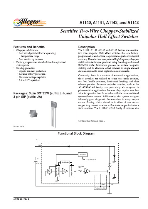
A1140, A1141, A1142, and A1143Sensitive Two-Wire Chopper-StabilizedUnipolar Hall Effect SwitchesA1140, A1141, A1142, and A1143features on-chip transient protection and a Zener clamp to protect against overvoltage conditions on the supply line.The output currents of the A1141 and A1143 switch HIGH in the presence of a south (+) polarity magnetic field of sufficient strength, and switch LOW otherwise, as in the presence of a weak field or a north (–) polarity field. The other two devices in the family (A1140 and A1142) have an opposite output: the currents switch LOW in the presence of a south-polarity magnetic field of sufficient strength,and switch HIGH otherwise. The other differences in the switches are their defined low current levels and magnetic switchpoints.All versions are offered in two package styles. The LH is a SOT-23W, miniature low-profile package for surface-mount applications. The UA is a three-lead ultramini SIP for through-hole mounting. Each package is available in a lead (Pb) free version (suffix, –T ) with 100% matte tin plated leadframe. Field-programmable versionsalso available: A1180, A1181, A1182, and A1183.Absolute Maximum RatingsCharacteristicSymbol NotesRating Units Supply Voltage V CC 28V Reverse Supply Voltage V RCC –18V Magnetic Flux DensityB Unlimited G Operating Ambient Temperature T A Range E –40 to 85ºC Range L–40 to 150ºC Maximum Junction Temperature T J (max)165ºC Storage TemperatureT stg–65 to 170ºCDescription (continued)1. VCC2. No connection3. GND1. VCC2. GND3. GNDPackage LH, 3-pin SOT Package UA, 3-pin SIPSensitive Two-Wire Chopper-StabilizedUnipolar Hall Effect SwitchesA1140, A1141, A1142, and A1143Part Number Pb-Free 1Packing 2Package Operating Ambient Temperature, T A(°C)Output Level in South (+) Field 3Supply Current at Low Output, I CC(L)(mA)A1140EUATI-T 4Yes Tape and Reel, 2000 pieces/reel Through Hole –40 to 85Low2 to 5A1140LUATI-T 4Yes Tape and Reel, 2000 pieces/reel Through Hole –40 to 150A1141EUATI-T 4Yes Tape and Reel, 2000 pieces/reel Through Hole –40 to 85HighA1141LUATI-T 4Yes Tape and Reel, 2000 pieces/reel Through Hole –40 to 150A1142ELHLT-T Yes Tape and Reel, 3000 pieces/reel Surface Mount –40 to 85Low5 to 6.9A1142EUA-T Yes Bulk Bag, 500 pieces/bag Through Hole A1142EUATI-T 4Yes Tape and Reel, 2000 pieces/reel A1142LLHLT-T Yes Tape and Reel, 3000 pieces/reel Surface Mount –40 to 150A1142LUA-T Yes Bulk Bag, 500 pieces/bag Through Hole A1142LUATI-T 4Yes Tape and Reel, 2000 pieces/reel A1143ELHLT-T Yes Tape and Reel, 3000 pieces/reel Surface Mount –40 to 85HighA1143EUA-T Yes Bulk Bag, 500 pieces/bag Through Hole A1143EUATI-T 4Yes Tape and Reel, 2000 pieces/reel A1143LLHLT-T Yes Tape and Reel, 3000 pieces/reel Surface Mount –40 to 150A1143LUA-T Yes Bulk Bag, 500 pieces/bag Through HoleA1143LUATI-T 4YesTape and Reel, 2000 pieces/reelPb-based variants are being phased out of the product line.(a) Certain variants cited in this footnote are in production but have been determined to be NOT FOR NEW DESIGN. This classification indicates that sale of this device is currently restricted to existing customer applications. The device should not be purchased for new design applications because obsolescence in the near future is probable. Samples are no longer available. Status change: May 1, 2006. These variants include A1140EUATI, A1140LUATI, A1140LUATI, A1141EUA, A1141EUATI, A1141LLHLT, A1141LUA, A1141LUATI, A1142EUATI, A1142LUATI,A1142LLHLT, A1142LUA, A1143EUATI, A1143LUA , and A1143LUATI.(b) Certain variants cited in this footnote are in production but have been determined to be LAST TIME BUY . This classification indicates that the product is obsolete and notice has been given. Sale of this device is currently restricted to existing customer applications. The device should not be purchased for new design applications because of obsolescence in the near future. Samples are no longer available. Status date change October 31, 2006. Deadline for receipt of LAST TIME BUY orders is April 27, 2007. These variants include: A1142ELHLT, A1142EUA, A1143ELHLT, A1143EUA, and A1143LLHLT.2Contact Allegro for additional packing options.3South (+) magnetic fields must be of sufficient strength.4Some restrictions may apply to certain types of sales. Contact Allegro for details.5The sensors listed in this footnote are available only in limited distribution. Interested customers should contact the appropriate sales person or field application engineer for more information on availability. These variants include: A1140ELHLT-T, A1140EUA-T, A1140LLHLT-T, A1140LUA-T, A1141ELHLT-T, A1141EUA-T, A1141LLHLT-T, and A1141LUA-T.Product Selection GuideSensitive Two-Wire Chopper-StabilizedUnipolar Hall Effect SwitchesA1140, A1141, A1142, and A1143ELECTRICAL CHARACTERISTICS over the operating voltage and temperature ranges, unless otherwise specifiedCharacteristicSymbol Test ConditionsMin.Typ.Max.Units Supply Voltage 1V CC 3.5–24V Supply Current 2I CC(L)B>B OP for A1140; B<B RP for A1141 2–5mA B>B OP for A1142; B<B RP for A1143 5-– 6.9mA I CC(H)B>B OP for A1141, A1143B<B RP for A1140, A114212-–17mA Reverse Supply Current I RCCV RCC = –18 V –––1.6mA Supply Zener Clamp Voltage V ZSUPPLY I CC = I CC(L)(max) + 3 mA; T A = 25°C 28–40V Supply Zener Clamp Current I ZSUPPLY V ZSUPPLY = 28 V––I CC(L)(max) + 3 mAmA Output Slew Rate 3di/dt Capacitance of the oscilloscope performing the measurement = 20 pF–36–mA/μs Chopping Frequency f C –200–kHz Power-On Time 3t on C BYPASS = 0.01 μF––25μs Power-On State 5,6POSt < t on ; V CC slew rate > 25 mV/μs–HIGH––1V CCrepresents the generated voltage between the VCC pin and the GND pin.2Relative values of B use the algebraic convention, where positive values indicate south magnetic polarity, and negative values indicate north magneticpolarity; therefore greater B values indicate a stronger south polarity field (or a weaker north polarity field, if present).3Measured without bypass capacitor between VCC and GND. Use of a bypass capacitor results in slower current change. 3Measured with and without bypass capacitor of 0.01 μF. Adding a larger bypass capacitor causes longer Power-On Time.5POS is defined as true only with a VCC slew rate of 25 mV/ μs or greater. Operation with a V CC slew rate less than 25 mV / μs can permanently harm device performance.6POS is undefined for t > t on or B RP < B < B OP.MAGNETIC CHARACTERISTICS over the operating voltage and temperature ranges, unless otherwise specifiedCharacteristicSymbol Test ConditionsMin.Typ.*Max.Units Operate PointB OPA1140, A1142I CC = I CC(L) 5080110GA1141, A1143I CC = I CC(H) Release Point B RP A1140, A1142I CC = I CC(H) 4565105G A1141, A1143I CC = I CC(L) HysteresisB HYSB HYS = B OP – B RP51530G*Typical data are for initial design estimations only, and assume optimum manufacturing and application conditions, such as T A = 25°C and V CC = 12 V.Performance may vary for individual units, within the specified maximum and minimum limits.Sensitive Two-Wire Chopper-StabilizedUnipolar Hall Effect SwitchesA1140, A1141, A1142, and A1143Characteristic DataSensitive Two-Wire Chopper-StabilizedUnipolar Hall Effect SwitchesA1140, A1141, A1142, and A1143THERMAL CHARACTERISTICS may require derating at maximum conditions, see application informationCharacteristicSymbolTest Conditions*Value Units Package Thermal ResistanceR θJAPackage LH, 1-layer PCB with copper limited to solder pads 228ºC/W Package LH, 2-layer PCB with 0.463 in.2 of copper area each side connected by thermal vias110ºC/W Package UA, 1-layer PCB with copper limited to solder pads165ºC/W*Additional thermal information available on Allegro Web site.6789234510111213141516171819202122232425M a x i m u m A l l o w a b l e V C C (V )Power Derating CurveV CC(min)V CC(max)100200300400500600700800900100011001200130014001500160017001800190020406080100120140160180Temperature (°C)P o w e r D i s s i p a t i o n ,P D (m W )Power Dissipation versus Ambient TemperatureSensitive Two-Wire Chopper-StabilizedUnipolar Hall Effect SwitchesA1140, A1141, A1142, and A1143Functional DescriptionHYS I CC(H)I C CI CC(L)I+(A) A1140, A1142HYSI CC(H)I C CI CC(L)I+(B) A1141, A1143OperationThe output, I CC , of the A1140 and A1142 devices switch low after the magnetic field at the Hall sensor exceeds the operate point threshold, B OP . When the magnetic field is reduced to below the release point threshold, B RP , the device output goes high. The differences between the magnetic operate and release point is called the hysteresis of the device, B HYS . This built-in hysteresis allows clean switching of the output even in the presence of external mechanical vibration and electrical noise. The A1141 and A1143 devices switch with opposite polarity for similar B OP and B RP values, in comparison to the A1140 and A1142 (see figure 1).Figure 1. Alternative switching behaviors are available in the A114x device family. On the horizontal axis, the B+ direction indicates increasing south polarity magnetic field strength, and the B– direction indicates decreasing south polarity field strength (including the case of increasing north polarity).Sensitive Two-Wire Chopper-StabilizedUnipolar Hall Effect SwitchesA1140, A1141, A1142, and A1143Chopper Stabilization TechniqueWhen using Hall-effect technology, a limiting factor for switchpoint accuracy is the small signal voltage developed across the Hall element. This voltage is disproportionally small relative to the offset that can be produced at the output of the Hall sensor. This makes it difficult to process the signal while maintaining an accurate, reliable output over the specified oper-ating temperature and voltage ranges.Chopper stabilization is a unique approach used to minimize Hall offset on the chip. The patented Allegro technique, namely Dynamic Quadrature Offset Cancellation, removes key sources of the output drift induced by thermal and mechanical stresses. This offset reduction technique is based on a signal modulation-demodulation process. The undesired offset signal is separated from the magnetic field-induced signal in the frequency domain, through modulation. The subsequent demodulation acts as a modulation process for the offset, causing the magnetic field-induced signal to recover its original spectrum at baseband, while the dc offset becomes a high-frequency signal. The magnetic-sourced signal then can pass through a low-pass filter, while the modulated dc offset is suppressed. This configuration is illus-trated in figure 2.The chopper stabilization technique uses a 200 kHz highfrequency clock. For demodulation process, a sample and hold technique is used, where the sampling is performed at twice the chopper frequency (400 kHz). This high-frequency operation allows a greater sampling rate, which results in higher accuracy and faster signal-processing capability. This approach desensi-tizes the chip to the effects of thermal and mechanical stresses, and produces devices that have extremely stable quiescent Hall output voltages and precise recoverability after temperature cycling. This technique is made possible through the use of a BiCMOS process, which allows the use of low-offset, low-noise amplifiers in combination with high-density logic integration and sample-and-hold circuits.The repeatability of magnetic field-induced switching is affected slightly by a chopper technique. However, the Allegro high-frequency chopping approach minimizes the affect of jitter and makes it imperceptible in most applications. Applications that are more likely to be sensitive to such degradation are those requiring precise sensing of alternating magnetic fields; forexample, speed sensing of ring-magnet targets. For such applica-tions, Allegro recommends its digital sensor families with lower sensitivity to jitter. For more information on those devices, contact your Allegro sales representative.Figure 2. Chopper stabilization circuit (Dynamic Quadrature Offset Cancellation)HallSensitive Two-Wire Chopper-StabilizedUnipolar Hall Effect SwitchesA1140, A1141, A1142, and A1143Application InformationFor additional general application information, visit the Allegro Web site at www. .0.01μFUA Onlyseparation 5mmBYP Figure 3. Typical application circuitTypical Application CircuitThe A114x family of devices must be protected by an external bypass capacitor, C BYP , connected between the supply, VCC, and the ground, GND, of the device. C BYP reduces both external noise and the noise generated by the chopper-stabilization func-tion. As shown in figure 3, a 0.01 μF capacitor is typical.Installation of C BYP must ensure that the traces that connect it to the A114x pins are no greater than 5 mm in length.All high-frequency interferences conducted along the supply lines are passed directly to the load through C BYP , and it serves only to protect the A114x internal circuitry. As a result, the load ECU (electronic control unit) must have sufficient protection, other than C BYP , installed in parallel with the A114x.A series resistor on the supply side, RS (not shown), in combina-tion with C BYP , creates a filter for EMI pulses.When determining the minimum V CC requirement of the A114x device, the voltage drops across R S and the ECU sense resistor, R SENSE , must be taken into consideration. The typical value for R SENSE is approximately 100 Ω.Sensitive Two-Wire Chopper-StabilizedUnipolar Hall Effect SwitchesA1140, A1141, A1142, and A1143Power DeratingThe device must be operated below the maximum junctiontemperature of the device, T J(max). Under certain combinations of peak conditions, reliable operation may require derating sup-plied power or improving the heat dissipation properties of the application. This section presents a procedure for correlating factors affecting operating T J . (Thermal data is also available on the Allegro MicroSystems Web site.)The Package Thermal Resistance, R θJA , is a figure of merit sum-marizing the ability of the application and the device to dissipate heat from the junction (die), through all paths to the ambient air. Its primary component is the Effective Thermal Conductivity, K, of the printed circuit board, including adjacent devices and traces. Radiation from the die through the device case, R θJC , is relatively small component of R θJA . Ambient air temperature, T A , and air motion are significant external factors, damped by overmolding.The effect of varying power levels (Power Dissipation, P D ), can be estimated. The following formulas represent the fundamental relationships used to estimate T J , at P D . P D = V IN × I IN (1)ΔT = P D × R θJA (2)T J = T A + ΔT(3)For example, given common conditions such as: T A = 25°C,V CC = 12 V, I CC = 4 mA, and R θJA = 140 °C/W, then: P D = V CC × I CC = 12 V × 4 mA = 48 mW ΔT = P D × R θJA = 48 mW × 140 °C/W = 7°CT J = T A + ΔT = 25°C + 7°C = 32°CA worst-case estimate, P D(max), represents the maximum allow-able power level (V CC(max), I CC(max)), without exceeding T J(max), at a selected R θJA and T A .Example : Reliability for V CC at T A = 150°C, package UA, using minimum-K PCB.Observe the worst-case ratings for the device, specifically: R θJA = 165°C/W, T J(max) = 165°C, V CC(max) = 24 V , and I CC(max) = 17 mA.Calculate the maximum allowable power level, P D(max). First, invert equation 3:ΔT max = T J(max) – T A = 165 °C – 150 °C = 15 °CThis provides the allowable increase to T J resulting from internal power dissipation. Then, invert equation 2:P D(max) = ΔT max ÷ R θJA = 15°C ÷ 165 °C/W = 91 mW Finally, invert equation 1 with respect to voltage: V CC(est) = P D(max) ÷ I CC(max) = 91 mW ÷ 17 mA = 5 V The result indicates that, at T A , the application and device can dissipate adequate amounts of heat at voltages ≤V CC(est).Compare V CC(est) to V CC(max). If V CC(est) ≤ V CC(max), then reli-able operation between V CC(est) and V CC(max) requires enhanced R θJA . If V CC(est) ≥ V CC(max), then operation between V CC(est) and V CC(max) is reliable under these conditions.Sensitive Two-Wire Chopper-StabilizedUnipolar Hall Effect SwitchesA1140, A1141, A1142, and A1143Device Qualification ProgramEMC (Electromagnetic Compatibility) RequirementsTest NameReference Specification ESD – Human Body Model AEC-Q100-002ESD – Machine Model AEC-Q100-003Conducted Transients ISO 7637-2Direct RF Injection ISO 11452-7Bulk Current Injection ISO 11452-4TEM CellISO 11452-3Contact Allegro for information.Contact your local representative for EMC results.Sensitive Two-Wire Chopper-StabilizedUnipolar Hall Effect SwitchesA1140, A1141, A1142, and A1143Package LH, 3-Pin; (SOT-23W)Sensitive Two-Wire Chopper-StabilizedUnipolar Hall Effect SwitchesA1140, A1141, A1142, and A1143The products described herein are manufactured under one or more of the following U.S. patents: 5,045,920; 5,264,783; 5,442,283; 5,389,889; 5,581,179; 5,517,112; 5,619,137; 5,621,319; 5,650,719; 5,686,894; 5,694,038; 5,729,130; 5,917,320; and other patents pending.Allegro MicroSystems, Inc. reserves the right to make, from time to time, such de p ar t ures from the detail spec i f i c a t ions as may be required to permit improvements in the per f or m ance, reliability, or manufacturability of its products. Before placing an order, the user is cautioned to verify that the information being relied upon is current.Allegro products are not authorized for use as critical components in life-support devices or sys t ems without express written approval. The in f or m a t ion in c lud e d herein is believed to be ac c u r ate and reliable. How e v e r, Allegro MicroSystems, Inc. assumes no re s pon s i b il i t y for its use; nor for any in f ringe m ent of patents or other rights of third parties which may result from its use. Copyright © 2004, 2006 Allegro MicroSystems, Inc.Package UA, 3-Pin SIP。
MA4ST1240-1141T中文资料

260°C reflow compatibility
Also Offering s Compliant Equivalent Parts
1.00 0.80 0.60
MA4ST1230/1231 MAVR-001230 MA4ST1240/1241 / MAVR-001240
Series Resistance (Ohm)
0.40
0.20
0.00
0.0
0.5
1.0
1.5
2.0
2.5
3.0
Biasing Voltage (V)
2
M/A-COM Inc. and its affiliates reserve the right to make changes to the product(s) or information contained herein without notice. M/A-COM makes no warranty, representation or guarantee regarding the suitability of its products for any particular purpose, nor does M/A-COM assume any liability whatsoever arising out of the use or application of any product(s) or information.
Typical Capacitance vs. Biasing Voltage
Si114x-中文手册

说明
阀门控制 烟雾探测器 非接触开关 非接触滑动器 占位传感器 消费类电子设备 工业自动化 显示屏背光控制 光中断器
Si1141/42/43 是基于反射的低功率红外线临近和环境光传感器,带有 I2C 数字接口和 可编程事件中断输出。此非接触传感器 IC 包括模拟到数字转换器、集成高灵敏度可 见和红外线光电二极管 、数字信号处理器和具有十五个可选驱动电平的一个、两个或 三个集成红外线 LED 驱动器。Si1141/42/43 在广泛的动态范围和包括阳光直射在内 的各种光源下可提供优异性能。Si1141/42/43 还可以在深色玻璃盖下工作。光电二极 管响应和关联的数字转换电路对人造光闪烁噪声和自然光颤动噪声具有优异的抗扰 性。Si1142/43 具有两个或多个 LED,能够支持多轴式临近运动探测。Si1141/42/43 器件 在 10 引 线 2x2 mm QFN 封装 中提 供,能够 在 –40 至 +85 °C 温 度 范围 中在 1.71 至 3.6 V 的条件下运行。
四方综保电动机说明书
第一章概述CSF106VD21数字式电动机保护主要用于2000kW以下不设纵差保护的高压异步电动机,亦可作2000kW以上的异步机或同步机的后备保护。
表1-1 CSF106VD系列数字式电动机保护功能配置CSF106VD22同步电动机综合保护,在CSFVD21基础上将速断保护改为差动保护,适用于任何容量的同步电动机,除具有上述异步电动机综合保护功能外,还具有保护动作跳励磁回路灭磁开关输出接口和同步电动机失步联跳电动机高压开关的输入接口,同步电动机失磁信号输入接口。
装置设有RS232、RS485及LONWORKS接口可与监控系统连接,便于实现四遥及远方通讯。
定时全面的自检系统大大提高了保护的可靠性。
同时,本装置支持GPS(全球卫星定位系统)对时。
其主要的技术特点如下:1)以工业级32位MPU单片机系统为核心部件,采用内部总线方式,芯片内设有ADC、32位CPU、QSM、SRAM、TPURAM、TPU、FLASH EEPROM,总线不出芯片,外围电路全部光藕隔离,采集8路模拟量,占用CPU时间不超过1us,高精度、高速率,可扩展到16路模拟量,在线程序写入FLASH芯片(ISP),方便软件修改、升级。
2)128×64点大液晶全汉字显示,调试全部为汉字菜单结构,使用方便、直观、信息详尽丰富。
3)采用工业级芯片,表面贴工艺,体积小,抗震、抗干扰能力强、可靠性高。
4)前面板232串口带光电隔离,可在现场实现通讯,提供更加方便友好的调试操作环境。
5)结构上设计合理,全封闭机箱坚固、抗震、抗干扰能力强,机箱小巧,适合安装于保护屏、开关柜等处。
6)该保护共可录入4套保护定值,便于现场运行。
7)可扩展工业级CAN总线,LON总线网络,组网方便、经济、可靠、可与监控系统直接通讯。
8)自动记录故障数据,掉电不丢失,便于事故分析。
9)线路故障时,除提供光报信号外,保护自动弹出全中文故障报告,直观明了,便于维护。
MXT2144中文手册

1、特点z分辨率:14 bitz工作电压:3.3V电源z转换速率:可达210MHzz满量程输出电流可调整范围:2mA~20mAz输入类型:并行输入z工作模式:电流型z功耗:150mW@3.3Vz兼容AD97442、功能描述MXT2144是一种14位电流输出型、CMOS D/A转换器,最大刷新率至少可达200MSPS,工作电压支持3.3伏,在3.3伏电压下工作时功耗小于160毫瓦。
在待机模式下,其功耗约为20mW。
该D/A转换器采用了分段电流沉结构,可以有效的减小电流开关的数量,从而减小开关电流的浪涌,改善建立时间,提高转换器的精度.该D/A转换器主要应用在通讯、仪器仪表、高分辨率图像系统、波形发生器等方面。
该电路在工作时,输入的14位数字信号存放在内部寄存器,然后控制电流源阵列的电流源打开或关断,从而控制电流的增加或减小。
整个电路可以分为电压基准源、偏置电路、电流源阵列、电流开关和高速锁存器等部分。
MXT2144内部寄存器在时钟上升沿进行刷新。
如果驱动时钟或数字输入的线电阻有50Ω,为了减小反射,建议在管脚附近用50Ω电阻接地。
另外,也建议把数字电源与模拟电源,数字地与模拟地分开,以使其性能最优化。
为了减小电源噪声,最好在靠近AVDD和DVDD管脚处分别对模拟地和数字地接0.1uF的电容。
MXT2144内部带隙电压参考源为1.22V,在整个温度范围温度系数为±50ppm/℃。
管脚16 VREFLO是参考选择端,如果VREFLO接地,则为内部参考;若接模拟电源,则为使用外部参考源,由17管脚输入。
输出I OUT的电流由18管脚的FSADJ端所接的R SET来设置,满量程范围为2~20mA可调。
如果采用内部参考,则V FSADJ约为1.22V;如用外部参考,则V FSADJ约等于外参考电压。
满量程输出电流 I OUTFS=(V FSADJ/R SET) X 32当满量程电流为20mA时,输入码与输出电流的对应关系表(表1):表1INPUT CODE(D13-D0) IOUTA(mA) IOUTB(mA)1111 11111 11111 20 01000 00000 00000 10 100000 00000 00000 0 20IOUTA与IOUTB为互补电流输出端,它们的和总是等于满量程电流减去1LSB。
产品

扩展模块MES114 MES120 MES120G MES114E MES114F施耐德Sepam综合保护装置可用于进出线、变压器、电动机、母线和电容器,带液晶显示屏的中文人机界面,符合用户的使用习惯,模块化设计,功能可由选择模块的增加而扩张,方便安装Sepam综合保护及系统Sepam综合保护装置Sepam 10系列S10N Sepam S10N带液晶显示器本体S10B Sepam S10B带液晶显示器本体S10A Sepam S10A带液晶显示器本体Sepam 20系列S20 Sepam S20带液晶显示器本体T20 Sepam T20带液晶显示器本体M20 Sepam M20带液晶显示器本体B21 Sepam B21带液晶显示器本体B22 Sepam B22带液晶显示器本体Sepam 40系列S40 Sepam S40带液晶显示器本体S41 Sepam S41带液晶显示器本体S42 Sepam S42带液晶显示器本体S43 Sepam S43带液晶显示器本体T40 Sepam T40带液晶显示器本体T42 Sepam T42带液晶显示器本体M41 Sepam M41带液晶显示器本体G40 Sepam G40带液晶显示器本体Sepam 80系列S80 Sepam S80带液晶显示器本体S81 Sepam S81带液晶显示器本体S82 Sepam S82带液晶显示器本体S84 Sepam S84带液晶显示器本体T81 Sepam T81带液晶显示器本体T82 Sepam T82带液晶显示器本体T87 Sepam T87带液晶显示器本体Z82 Sepam Z82带液晶显示器本体M81 Sepam M81带液晶显示器本体M87 Sepam M87带液晶显示器本体M88 Sepam M88带液晶显示器本体G82 Sepam G82带液晶显示器本体G87 Sepam G87带液晶显示器本体G88 Sepam G88带液晶显示器本体B80 Sepam B80带液晶显示器本体B83 Sepam B83带液晶显示器本体C86 Sepam C86带液晶显示器本体Sepam附件模块CCA630用于1A或5A电流互感器CCA634用于1A或5A电流互感器和零序电流互感器CCT640用于B21、B22和B83,电压输入模块MES114 10开关量输入/4开关量输出模块,24-250VDCMES114E 10开关量输入/4开关量输出模块,110-125VDC/ACMES114F 10开关量输入/4开关量输出模块,220-250VDCMES120 14开关量输入/6开关量输出模块,24-250VDCMES120G 14开关量输入/6开关量输出模块,220-250VDCMES120H 14开关量输入/6开关量输出模块,110-125VDCMET148-2 8温度传感器型号输入模块MSA141模拟输出模块ACE949-2 2线RS485通讯模块(Modbus接口)ACE937光钎通讯接口ACE959 4线RS485通讯模块(Modbus接口)ACE969TP 2线RS485通讯模块(Modbus,DPN3或IEC 60870-5-103多协议接口) ACE969FO光钎通讯接口(Modbus,DPN3或IEC 60870-5-103多协议接口)SFT2841 SFT2841调试软件CCA783 Sepam与PC间调试电缆CCA612通讯连接电缆CSH30二次侧5A/1A零序互感转换器CSH120零序互感器,内劲120mmCSH200零序互感器,内劲200mm网络通讯设备EGX100MG以太网关(Modbus/TCP)EGX300MG以太网关(Modbus/TCP),内置web页EGX400MG以太网关(Modbus/TCP,带光纤口),内置web页EG102多串口服务器(2个RS485接口,1个以太网口)EG116多串口服务器(16个RS485接口,1个以太网口)EG132多串口服务器(32个RS485接口,1个以太网口)NCM-18E4通讯管理机18个RS232/RS422/RS485串口,4个RJ45以太网口NCM-16E2通讯管理机16个RS232/RS422/RS485串口,2个RJ45以太网口NCM-08E2C2通讯管理机8个RS232/RS422/RS485串口,2个RJ45以太网口,2个CAN接口NCM-08E2通讯管理机8个RS232/RS422/RS485串口,2个RJ45以太网口NCM-04E1通讯管理机4个RS232/RS422/RS485串口,1个RJ45以太网口电力系统模拟屏MSP100马赛克静态模拟屏MSP200马赛克动态模拟屏LSP100 LED双基色模拟屏LSD200 LED全色彩模拟屏施耐德PowerLogic电力监控系统详细介绍:PowerLogic电力监控系统PM800系列电力参数测量仪及模块PM810MG 全电量测量、1DI,1DO,Modbus/RS485通讯,大液晶屏显示PM820MG PM810全部功能、谐波分析、时钟、数据和报警记录PM850MG PM820全部功能、波形捕捉、负荷趋势预测PM870MG PM850全部功能、电压的下陷和骤升监测PM810LOG PM810的扩展模块,谐波分析,时钟,数据和报警记录PM8M22 PM800系列的IO扩展模块,2DI、2DOPM8M26 PM800系列的IO扩展模块,6DI、2DOPM8M2222 PM800系列的IO扩展模块,2DI、2DO、2AI、2AOPM8ECC PM800系列的以太网关扩展模块,1个以太网口,1个RS485接口内置WEB浏览器,以太网关功能PM700系列电力参数测量仪PM700MG 全电量测量、THD、Max/Min、大屏幕液晶显示PM700PMG PM700全部功能、2个脉冲输出PM710MG PM700全部功能、Modbus/RS485通讯PM750MG PM710全部功能、2DIPM200系列电力参数测量仪PM200MG 全电量测量、大屏幕液晶显示PM200PMG PM200全部功能、2个脉冲输出PM210MG PM200全部功能、Modbus/RS485通讯PM9系列电力参数测量仪PM9 全参数测量+电能计量PM9C 全参数测量+电能计量+通讯功能PM9P 全参数测量+电能计量+远程脉冲输出MC系列多回路监控单元MC09 测量9个电流和母线电压(三相L-N和L-L),电压电流报警,Modbus/RS485通讯MC18 18DI,Modbus/RS485通讯MC08 8DI,8DO,Modbus/RS485通讯Sepam1000+T81 Sepam1000+T81 Sepam1000+T81 Sepam1000+T87 Sepam1000+T87 Sepam1000+T87Sepam1000+M81 Sepam1000+M81 Sepam1000+M81 Sepam1000+M87 Sepam1000+M87 Sepam1000+M87Sepam1000+S82 Sepam1000+S82 Sepam1000+S82 Sepam1000+G87 Sepam1000+G87 Sepam1000+G87Sepam1000+T82 Sepam1000+T82 Sepam1000+T82 Sepam1000+C86 Sepam1000+C86 Sepam1000+C86Sepam1000+G82 Sepam1000+G82 Sepam1000+G82 Sepam1000 S20 Sepam1000 S20 Sepam1000 S20Sepam1000+M88 Sepam1000+M88 Sepam1000+M88 Sepam1000 M20 Sepam1000 M20 Sepam1000 M20Sepam1000+G88 Sepam1000+G88 Sepam1000+G88 Sepam1000 S40 Sepam1000 S40 Sepam1000 S40Sepam1000+S84 Sepam1000+S84 Sepam1000+S84 Sepam1000 S42 Sepam1000 S42 Sepam1000 S42Sepam1000+Z82 Sepam1000+Z82 Sepam1000+Z82 Sepam1000 T40 Sepam1000 T40 Sepam1000 T40Sepam1000+T87 Sepam1000+T87 Sepam1000+T87 SEPAM1000 T40 SEPAM1000 S80 SEPAM1000 B80SEPAM1000 B83 SEPAM1000 S81 SEPAM1000 T81 SEPAM1000 T42 SEPAM1000 G40 SEPAM1000 S40SEPAM1000 M81 SEPAM1000 S82 SEPAM1000 T82 SEPAM1000 M87 SEPAM1000 G87 SEPAM1000 C86Sepam1000+M87 Sepam1000+M87 Sepam1000+M87 SEPAM1000 T87 SEPAM1000 M88 SEPAM1000 G88Sepam1000+G87 Sepam1000+G87 Sepam1000+G87 SEPAM1000 G82 SEPAM1000 S84 SEPAM1000 Z82Sepam1000+C86 Sepam1000+C86 Sepam1000+C86 SEPAM1000 M41 SEPAM1000 S42 SEPAM1000 S43SEPAM1000 S20 SEPAM1000 T20 SEPAM1000 M20 SEPAM1000 B21 SEPAM1000 B22 SEPAM1000 S41ACE949-2 ACE959 ACE937 ACE969 MES114 MES114E MES114F MSA141 CSH120CSH200 CSH30 CCA612 CCA770 CCA772 CCA774 MET148-2 CCA630 CCA634PM电力表:PM810MG PM820G PM850G PM870G PM810LOG PM8M22PM8M26 PM8M2222 PM700MG PM700PMG PM710MG PM750MG PM200MG PM200PMG PM210MG MC09 MC18 MC08。
梅格 SMRT410 继电保护测试系统 用户手册说明书

SMRT410继电保护测试系统g 小巧,坚固,轻便,功能强大g 可连接计算机操作或独立操作g 带智能触屏界面,能直观手动操作g每相大电流、高功率输出(60 Amps/300 VA rms)g灵活的输出设计,可提供多达四相电压和十相电流输出g 提供具有IEC 61850 测试能力的网络接口g使用AVTS软件实现全自动化测试仪器说明SMRT410将大恒流输出电压和大电流输出「智能」结合,可以测试各种机电式、固态式和基于微处理器的过电流继电器,包括电压控制继电器,电压阻尼继电器和高阻抗方向接地过流保护。
SMRT410为测试保护系统提供了完全的多相测试系统。
具有4路电压通道和6路电流通道,可以满足任何测试需要。
VIGEN模块在电流和电压通道都提供了高功率性能,可以测试几乎所有类型的保护继电器。
测试系统可以通过增加电压-电流、「VIGEN」模块的数目定制,以满足特定的测试需要。
SMRT410测试系统使用Megger全新智能触摸界面STVI (Smart Touch View Interface™ ),拥有手动控制的功能。
STVI具有大屏幕、全彩、高分辨率和彩色液晶触摸屏等特点,这使用户可以快速进行手动测试、稳态和动态测试,也使手动测试屏使用简单,同时它也内置目前最普遍的各种继电器的预设置测试程序。
STVI使继电器测试不再需要连接计算机。
通过菜单屏幕和触摸屏的功能按键,用户可以快速方便的选择所需的测试功能。
测试结果可以保存在STVI以便下载到记忆棒或打印测试报告。
Megger先进的可视化测试软件(AVTS)实现了SMRT410的全自动化测试。
AVTS是微软®Windows ® XP ® /Vista™/7兼容的软件程序,它的设计目的是管理Megger全新SMRT继电保护测试的各个方面。
应用每个电流通道200 VA下连续电流的额定值是30Amps,短时电流额定值则达到300 VA下 60 Amps 。
霍尔开关集成电路 SDC141 数据手册说明书
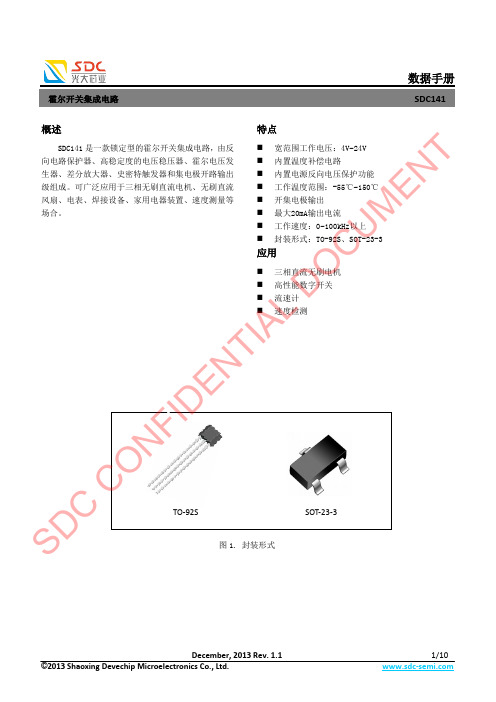
数据手册概述SDC141是一款锁定型的霍尔开关集成电路,由反向电路保护器、高稳定度的电压稳压器、霍尔电压发生器、差分放大器、史密特触发器和集电极开路输出级组成。
可广泛应用于三相无刷直流电机、无刷直流风扇、电表、焊接设备、家用电器装置、速度测量等场合。
特点⏹ 宽范围工作电压:4V ~24V ⏹ 内置温度补偿电路 ⏹ 内置电源反向电压保护功能 ⏹ 工作温度范围:-55℃~150℃ ⏹ 开集电极输出 ⏹ 最大20mA 输出电流⏹ 工作速度:0~100kHz 以上⏹封装形式:TO-92S 、SOT-23-3应用⏹ 三相直流无刷电机 ⏹ 高性能数字开关⏹ 流速计⏹速度检测图1. 封装形式SOT-23-3TO-92S SD CO NFID E N T I AL D OCUM EN T数据手册管脚描述GND VCCOUTPackage: SOT-23-3OUT VCCGND Package: TO-92S图2 管脚排布编号名称 功能 SOT-23-3TO-92S 1 1 VCC 电源 3 2 GND 地 23OUT输出脚表1. 管脚描述功能框图VCCGNDOUT图3. 功能框图SD CID E N T I AL D EN T数据手册订购信息SDC141Circuit TypeMagnetic Characteristics: A/a/BE1: Pb-freeG1: Halogen-freeTR: Tape ReelBlank: BulkX X-XPackageTO-92S: ZSSOT-23-3: JX封装温度范围产品编号标识编号包装形式无铅无卤无铅无卤TO-92S-55℃~150℃SDC141AZS-E1 SDC141AZS-G1 S41 S41G 袋装SDC141aZS-E1 SDC141aZS-G1 S41 S41G 袋装SDC141BZS-E1 SDC141BZS-G1 S41 S41G 袋装SOT-23-3 SDC141AJTR-E1 SDC141AJTR-G1 S41 S41G 编带SDC141aJTR-E1 SDC141aJTR-G1 S41 S41G 编带SDC141BJTR-E1 SDC141BJTR-G1 S41 S41G 编带S D CC ON FI DE NT IA LD OC UME NT数据手册极限参数(注意:应用不要超过最大值,以防止损坏。
- 1、下载文档前请自行甄别文档内容的完整性,平台不提供额外的编辑、内容补充、找答案等附加服务。
- 2、"仅部分预览"的文档,不可在线预览部分如存在完整性等问题,可反馈申请退款(可完整预览的文档不适用该条件!)。
- 3、如文档侵犯您的权益,请联系客服反馈,我们会尽快为您处理(人工客服工作时间:9:00-18:30)。
Package Cp (pF) 0.10 0.10 0.11 0.11 0.12 0.12
Package Ls (nH) 0.6 0.6 1.2 1.2 1.3 1.3
1
M/A-COM Inc. and its affiliates reserve the right to make changes to the product(s) or information contained herein without notice. M/A-COM makes no warranty, representation or guarantee regarding the suitability of its products for any particular purpose, nor does M/A-COM assume any liability whatsoever arising out of the use or application of any product(s) or information.
.
Absolute Maximum Ratings @ TA=+25 °C (Unless Otherwise Noted) 1
Parameter Reverse Voltage Forward Current Operating Temperature
Absolute Maximum 12 V 50 mA
Part Number
RoHs Compliant Part Number
Configuration Package
MA4ST1230-1141T MA4ST1240-1141T MA4ST1230CK-1146T MA4ST1240CK-1146T
MAVR-001230-12790T MAVR-001240-12790T
1.00 0.80 0.60MA4ST1230/1231 MAVR-001230 MA4ST1240/1241 / MAVR-001240
Series Resistance (Ohm)
0.40
0.20
0.00
0.0
0.5
1.0
1.5
2.0
2.5
3.0
Biasing Voltage (V)
2
M/A-COM Inc. and its affiliates reserve the right to make changes to the product(s) or information contained herein without notice. M/A-COM makes no warranty, representation or guarantee regarding the suitability of its products for any particular purpose, nor does M/A-COM assume any liability whatsoever arising out of the use or application of any product(s) or information.
Visit for additional data sheets and product information.
元器件交易网
Low Tuning Voltage/Low Rs Silicon Hyperabrupt Varactor Diode
SC-70 (3 lead)
MA4ST1200 Series V4
SOD-323
SC-79
Description
M/A-COM’s MA4ST1200 series is a highly repeatable, UHCVD/ion-implanted, hyperabrupt silicon tuning varactor in a cost effective surface mount package. This series of varactors is designed for high capacitance ratio, and high Q for low battery voltage operation. It is efficient for wide band tuning and low phase noise application where the supply voltage is limited to 5 volts or less. The Varactors are offered as Singles in SC-79, and SOD-323 along with a Common Cathode version offered in the SC-70, 3 Lead. These diodes are offered with standard Sn/Pb plating , as well as with 100% matte Sn plating on our RohS compliant equivalent devices.
Visit for additional data sheets and product information.
元器件交易网
Also Offering RoHs Compliant Equivalent Parts
Low Tuning Voltage/Low Rs Silicon Hyperabrupt Varactor Diode
MA4ST1231-1141T MA4ST1241-1141T MA4ST1231CK-1146T MA4ST1241CK-1146T
Single
SC-79
Single
SC-79
Single
SOD-323
Single
SOD-323
Common Cathode SC-70 (3L)
Common Cathode SC-70 (3L)
MA4ST1240 Ct (pF) 7.016 5.424 4.213 3.370 2.829 2.466 2.208 2.016 1.865 1.746
MA4ST1200 Series V4
Rs Cp
Cj Ls
Intrinsic Diode Model N=N Cj0=Cj0 Vj=Vj Fc=0.5 BV=20 V M=M Parasitic Cp & Ls Are per Above Table
Typical Capacitance Change vs. Temperature
4%
% of Capacitance Change (relative to 25 C)
2%
0%
-2%
-4%
-40
-15
10
35
60
85
Temperature (degree C)
3
• North America Tel: 800.366.2266 / Fax: 978.366.2266 • Europe Tel: 44.1908.574.200 / Fax: 44.1908.574.300 • Asia/Pacific Tel: 81.44.844.8296 / Fax: 81.44.844.8298
Typical Capacitance vs. Biasing Voltage
12
Capacitance (pF)
10
MA4ST1230/1231 /MAVR-001230 8
MA4ST1240/1241 /MAVR-001240
6
4
2
0
0
1
2
3
4
5
Biasing Voltage (V)
Typical Rs vs Biasing Voltage3
Part Number N
CJO
Vj
M
(pF)
(V)
MA4ST1230 1.1 MA4ST1240 1.1
12.7
3.136
2.6
8.65
3.170
2.6
3
M/A-COM Inc. and its affiliates reserve the right to make changes to the product(s) or information contained herein without notice. M/A-COM makes no warranty, representation or guarantee regarding the suitability of its products for any particular purpose, nor does M/A-COM assume any liability whatsoever arising out of the use or application of any product(s) or information.
• North America Tel: 800.366.2266 / Fax: 978.366.2266 • Europe Tel: 44.1908.574.200 / Fax: 44.1908.574.300 • Asia/Pacific Tel: 81.44.844.8296 / Fax: 81.44.844.8298
元器件交易网
Low Tuning Voltage/Low Rs Silicon Hyperabrupt Varactor Diode
Features
• Low Series Resistance at Low Tuning Voltages • High Capacitance Ratio at Low Tuning Voltages • Surface Mount Plastic Packages : SC-79, SOD-323,