2SB673中文资料
2SA1736中文资料
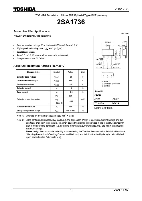
2SA1736
Power Amplifier Applications Power Switching Applications
2SA1736
Unit: mm
• Low saturation voltage: VCE (sat) = −0.5 V (max) (IC = −1.5 A) • High speed switching time: tstg = 0.2 μs (typ.) • Small flat package • PC = 1.0 to 2.0 W (mounted on a ceramic substrate) • Complementary to 2SC4541
3
2006-11-09
Collector current IC (A)
IC – VBE
−3.0 Common emitter
VCE = −2 V −2.5
−2.0
−1.5
Ta = 100°C
25
−25 −1.0
−0.5
0
0
−0.4
−0.8
−1.2
−1.6
−2.0
Base-emitter voltage VBE (V)
VCE (sat) – IC
−10
Common emitter
−3
IC/IB = 20
−1
−0.3
Ta = 100°C −0.1
−0.03
25 −25
−0.01 −1
−3 −10 −30 −100 −300 −1000 −3000
Collector current IC (mA)
2SA966资料

TOSHIBA Transistor Silicon PNP Epitaxial Type (PCT Process)2SA966Audio Power Amplifier Applications• Complementary to 2SC2236 and 3-W output applications.Absolute Maximum Ratings (Ta = 25°C)Characteristics Symbol Rating UnitCollector-base voltage V CBO −30 V Collector-emitter voltage V CEO −30 V Emitter-base voltage V EBO −5 V Collector current I C−1.5 AEmitter currentI E 1.5 A Collector power dissipation P C 900 mW Junction temperature T j 150 °C Storage temperature rangeT stg−55 to 150°CNote: Using continuously under heavy loads (e.g. the application of high temperature/current/voltage and the significant change in temperature, etc.) may cause this product to decrease in thereliability significantly even if the operating conditions (i.e. operating temperature/current/voltage, etc.) are within the absolute maximum ratings.Please design the appropriate reliability upon reviewing the Toshiba Semiconductor Reliability Handbook (“HandlingPrecautions”/Derating Concept and Methods) and individual reliability data (i.e. reliability test report and estimated failure rate, etc).Unit: mmJEDEC TO-92MOD JEITA ―TOSHIBA 2-5J1A Weight: 0.36 g (typ.)Electrical Characteristics (Ta = 25°C)Characteristics Symbol TestCondition MinTyp.Max UnitCollector cut-off current I CBO V CB = −30 V, I E = 0 ――−100nAEmitter cut-off current I EBO V EB = −5 V, I C = 0 ――−100nA Collector-emitter breakdown voltage V (BR) CEO I C = −10 mA, I B = 0 −30 ―― V Emitter-base breakdown voltage V (BR) EBO I E = −1 mA, I C = 0 −5 ―― VDC current gain h FE(Note)V CE = −2 V, I C = −500 mA 100 ― 320Collector-emitter saturation voltage V CE (sat)I C = −1.5 A, I B = −0.03 A ――−2.0V Base-emitter voltage V BE V CE = −2 V, I C = −500 mA ――−1.0V Transition frequency f T V CE = −2 V, I C = −500 mA ― 120 ― MHz Collector output capacitance C ob V CB = −10 V, I E = 0, f = 1 MHz ― 40 ― pF Note: h FE classification O: 100 to 200, Y: 160 to 320Markinglead (Pb)-free package orlead (Pb)-free finish.indicatorCollector current I C (mA)h FE – ICD C c u r re n t g a i n h F ECollector current I C (mA)V CE (sat) – I CC o l l e c t o r -e m i t t e r s a t u r a t i on v o l t a g eV C E (s a t ) (V )Base-emitter voltage V BE (V)I C – V BEC oll e c t o rc u r r e n t I C (m A )Ambient temperature Ta (°C)P C – TaC o l l e c t o r p owe r d i s s ip a t io n P C (W )Collector-emitter voltage V CE (V)Safe Operating AreaC o l l e c t o r c u r r e n t I C (A )1.00 0 20 40 60 80 100 120 140 160 1800.20.40.60.8−−−−−−−−−−−−−−−−−−Collector-emitter voltage V CE (V)I C – V CEC o l l e c t o r c u r r e n t I C (m A )−−−−−−−−−−−−−−−−−RESTRICTIONS ON PRODUCT USE20070701-EN •The information contained herein is subject to change without notice.•TOSHIBA is continually working to improve the quality and reliability of its products. Nevertheless, semiconductor devices in general can malfunction or fail due to their inherent electrical sensitivity and vulnerability to physical stress. It is the responsibility of the buyer, when utilizing TOSHIBA products, to comply with the standards of safety in making a safe design for the entire system, and to avoid situations in which a malfunction or failure of such TOSHIBA products could cause loss of human life, bodily injury or damage to property.In developing your designs, please ensure that TOSHIBA products are used within specified operating ranges as set forth in the most recent TOSHIBA products specifications. Also, please keep in mind the precautions and conditions set forth in the “Handling Guide for Semiconductor Devices,” or “TOSHIBA Semiconductor Reliability Handbook” etc.• The TOSHIBA products listed in this document are intended for usage in general electronics applications (computer, personal equipment, office equipment, measuring equipment, industrial robotics, domestic appliances, etc.).These TOSHIBA products are neither intended nor warranted for usage in equipment that requires extraordinarily high quality and/or reliability or a malfunction or failure of which may cause loss of human life or bodily injury (“Unintended Usage”). Unintended Usage include atomic energy control instruments, airplane or spaceship instruments, transportation instruments, traffic signal instruments, combustion control instruments, medical instruments, all types of safety devices, etc.. Unintended Usage of TOSHIBA products listed in his document shall be made at the customer’s own risk.•The products described in this document shall not be used or embedded to any downstream products of which manufacture, use and/or sale are prohibited under any applicable laws and regulations.• The information contained herein is presented only as a guide for the applications of our products. No responsibility is assumed by TOSHIBA for any infringements of patents or other rights of the third parties which may result from its use. No license is granted by implication or otherwise under any patents or other rights of TOSHIBA or the third parties.• Please contact your sales representative for product-by-product details in this document regarding RoHS compatibility. Please use these products in this document in compliance with all applicable laws and regulations that regulate the inclusion or use of controlled substances. Toshiba assumes no liability for damage or losses occurring as a result of noncompliance with applicable laws and regulations.。
2S系列三级管参数手册

160V 170V 60V 120V 40V 60V 50V 120V 80V 40V 60V 60V 60V 25V 160V 70V 120V 40V 80V 40V 60V 160V 160V 100V 60V 100V 80V 25V 100V 30V 40V 32V 32V 120V 150V 60V 160V 60V 120V 30V 120V 20V 180V 50V 60/30V 160V 160V
160/140V 160V 140V 140V 160V 160V 80V 160V 110V 80V 32V 50V 30V 32V 25V 35V 60V 110V 90V 130V 130V 110V 25V 200V 120V 120V 100V 25V 30V 25V 200V 100V 60V 25V 50V 100V 25V 100V 50V 30V 120V 160V 160V 100V 100V 150V 120V
100W 40W 120W 40W 0.2W 0.75W 25W 50W 10W 1W 1W 0.9W 0.9W 10W 35W 40W 0.9A 30W 200MHz 10W 0.4W 60W 70W 0.4W 40W 10W 10W 0.25W 0.35W 0.25W 80W 100W 90W 1W 0.75W 30W 40W 40W 80W 80W 90W 40W 30W 100W 0.9W 1W 40W
120W 150W 20W 20W 10W 15W 25W 20W 35W 100MHz 15W 20W 20W 10W 0.9W 20W 1W 1W 1W 1W 1W 70W 100W 30W 30W 25W 30W 320MHz 1W 0.3W 1.2W 1.2W 1.2W 1.8W 100W 30W 2.5W 25W 75W 2W 80W 1W 150W 1W 25W 150W 90W
2SB系列三极管参数
2SB系列三极管参数2SB1009 SI-P 40V 2A 10W 100MHz | 2SB1010 SI-P 40V 2A 0.75W 100MHz2SB1012K P-DARL 120V 1.5A 8W | 2SB1013 SI-P 20V 2A 0.7W2SB1015 SI-P 60V 3A 25W 0.4us | 2SB1016 SI-P 100V 5A 30W 5MHz2SB1017 SI-P 80V 4A 25W 9MHz | 2SB1018 SI-P 100V 7A 30W 0.4us2SB1020 P-DARL+D 100V 7A 30W 0.8us | 2SB1023 P-DARL+D 60V 3A 20W B=5K 2SB1035 SI-P 30V 1A 0.9W 100MHz | 2SB1039 SI-P 100V 4A 40W 20MHz2SB1050 SI-P 30V 5A 1W 120MHz | 2SB1055 SI-P 120V 6A 70W 20MHz2SB1065 SI-P 60V 3A 10W | 2SB1066 SI-P 50V 3A 1W 70MHz2SB1068 SI-P 20V 2A 0.75W 180MHz | 2SB1071 SI-P 40V 4A 25W 150MHz2SB1077 P-DARL 60V 4A 40W B>1K | 2SB1086 SI-P 160V 1.5A 20W 50MHz2SB1098 P-DARL+D 100V 5A 20W B=80 | 2SB1099 P-DARL+D 100V 8A 25W B=6K 2SB1100 P-DARL+D 100V 10A 30W B=6 | 2SB1109 SI-P 160V 0.1A 1.25W2SB1109S SI-P 160V 0.1A 1.25W | 2SB1117 SI-P 30V 3A 1W 280MHz2SB1120 SI-P 20V 2.5A 0.5W 250MHz | 2SB1121T SI-P 30V 2A 150MHz2SB1123 SI-P 60V 2A 0.5W 150MHz | 2SB1132 SI-P 40V 1A 0.5W 150MHz2SB1133 SI-P 60V 3A 25W 40MHz | 2SB1134 SI-P 60V 5A 25W 30W2SB1135 SI-P 60V 7A 30W 10MHz | 2SB1136 SI-P 60V 12A 30W 10MHz2SB1140 SI-P 25V 5A 10W 320MHz | 2SB1141 SI-P 20V 1.2A 10W 150MHz2SB1143 SI-P 60V 4A 10W 140MHz | 2SB1146 P-DARL 120V 6A 25W2SB1149 P-DARL 100V 3A 15W B=10K | 2SB1151 SI-P 60V 5A 20W2SB1154 SI-P 130V 10A 70W 30MHz | 2SB1156 SI-P 130V 20A 100W2SB1162 SI-P 160V 12A 120W | 2SB1163 SI-P 170V 15A 150W2SB1166 SI-P 60V 8A 20W 130MHz | 2SB1168 SI-P 120V 4A 20W 130MHz2SB1182 SI-P 40V 2A 10W 100MHz | 2SB1184 SI-P 60V 3A 15W 70MHz2SB1185 SI-P 50V 3A 25W 70MHz | 2SB1186 SI-P 120V 1.5A 20W 50MHz2SB1187 SI-P 80V 3A 35W | 2SB1188 SI-P 40V 2A 100MHz2SB1202 SI-P 60V 3A 15W 150MHz | 2SB1203 SI-P 60V 5A 20W 130MHz2SB1204 SI-P 60V 8A 20W 130MHz | 2SB1205 SI-P 25V 5A 10W 320MHz2SB1212 SI-P 160V 1.5A 0.9W 50MHz | 2SB1223 P-DARL+D 70V 4A 20W 20MHz2SB1236 SI-P 120V 1.5A 1W 50MHz | 2SB1237 SI-P 40V 1A 1W 150MHz2SB1238 SI-P 80V 0.7A 1W 100MHz | 2SB1240 SI-P 40V 2A 1W 100MHz2SB1243 SI-P 60V 3A 1W | 2SB1254 P-DARL 160V 7A 70W2SB1255 P-DARL 160V 8A 100W B>5K | 2SB1258 P-DARL+D 100V 6A 30W B>1K 2SB1274 SI-P 60V 3A 30W 100MHz | 2SB1282 P-DARL+D 100V 4A 25W 50MHz 2SB1292 SI-P 80V 5A 30W | 2SB1302 SI-P 25V 5A 320MHz2SB1318 P-DARL+D 100V 3A 1W B>200 | 2SB1326 SI-P 30V 5A 0.3W 120MHz2SB1329 SI-P 40V 1A 1.2W 150MHz | 2SB1330 SI-P 32V 0.7A 1.2W 100MHz2SB1331 SI-P 32V 2A 1.2W 100MHz | 2SB1353E SI-P 120V 1.5A 1.8W 50MHz2SB1361 SI-P 150V 9A 100W 15MHz | 2SB1370 SI-P 60V 3A 30W 15MHz2SB1373 SI-P 160V 12A 2.5W 15MHz | 2SB1375 SI-P 60V 3A 25W 9MHz2SB1382 P-DARL+D 120V 16A 75W B>2 | 2SB1393 SI-P 30V 3A 2W 30MHz2SB1420 SI-P 120V 16A 80W 50MHz | 2SB1425 SI-P 20V 2A 1W 90MHz2SB1429 SI-P 180V 15A 150W 10MHz | 2SB1434 SI-P 50V 2A 1W 110MHz2SB1468 SI-P 60/30V 12A 25W | 2SB1470 P-DARL 160V 8A 150W B>5K2SB1490 P-DARL 160V 7A 90W B>5K | 2SB1493 P-DARL 160/140V 7A 70W 20 2SB1503 P-DARL 160V 8A 120W B>5K | 2SB1556 P-DARL 140V 8A 120W B>5K 2SB1557 P-DARL 140V 7A 100W B>5K | 2SB1559 P-DARL 160V 8A 80W B>5K 2SB1560 P-DARL 160V 10A 100W 50MHz | 2SB1565 SI-P 80V 3A 25W 15MHz2SB1587 P-DARL+D 160V 8A 70W B>5K | 2SB1624 P-DARL 110V 6A 60W B>5K 2SB206 GE-P 80V 30A 80W | 2SB324 GE-P 32V 1A 0.25W2SB337 GE-P 50V 7A 30W LF-POWER | 2SB407 GE-P 30V 7A 30W2SB481 GE-P 32V 1A 6W 15KHz | 2SB492 GE-P 25V 2A 6W2SB511E SI-P 35V 1.5A 10W 8MHz | 2SB524 SI-P 60V 1.5A 10W 70MHz2SB527 SI-P 110V 0.8A 10W 70MHz | 2SB531 SI-P 90V 6A 50W 8MHz2SB536 SI-P 130V 1.5A 20W 40MHz | 2SB537 SI-P 130V 1.5A 20W 60MHz2SB541 SI-P 110V 8A 80W 9MHz | 2SB544 SI-P 25V 1A 0.9W 180MHz2SB546A SI-P 200V 2A 25W 5MHz | 2SB549 SI-P 120V 0.8A 10W 80MHz2SB557 SI-P 120V 8A 80W | 2SB560 SI-P 100V 0.7A 0.9W 100MHz2SB561 SI-P 25V 0.7A 0.5W | 2SB564 SI-P 30V 1A 0.8W2SB598 SI-P 25V 1A 0.5W 180MHz | 2SB600 SI-P 200V 15A 200W 4MHz2SB601 P-DARL 100V 5A 30W | 2SB605 SI-P 60V 0.7A 0.8W 120MHz2SB621 SI-N 25V 1.5A 0.6W 200MHz | 2SB621A SI-N 50V 1A 0.75W 200MHz2SB631 SI-P 100V 1A 8W | 2SB632 SI-P 25V 2A 10W 100MHz2SB633 SI-P 100V 6A 40W 15MHz | 2SB637 SI-P 50V 0.1A 0.3W 200MHz2SB641 SI-P 30V 0.1A 120MHz | 2SB647 SI-P 120V 1A 0.9W 140MHz2SB649A SI-P 160V 1.5A 1W 140MHz | 2SB656 SI-P 160V 12A 125W 20MHz2SB673 P-DARL+D 100V 7A 40W 0.8us | 2SB676 P-DARL 100V 4A 30W 0.15us 2SB681 SI-N 150V 12A 100W 13MHz | 2SB688 SI-P 120V 8A 80W 10MHz2SB700 SI-P 160V 12A 100W | 2SB703 SI-P 100V 4A 40W 18MHz2SB705 SI-P 140V 10A 120W 17MHz | 2SB707 SI-P 80V 7A 40W POWER2SB709 SI-P 45V 0.1A 0.2W 80MHz | 2SB716 SI-P 120V 0.05A 0.75W2SB720 SI-P 200V 2A 25W 100MHz | 2SB727 P-DARL+D 120V 6A 50W B>1K 2SB731 SI-P 60V 1A 10W 75MHz | 2SB733 SI-P 20V 2A 1W >50MHz2SB734 SI-P 60V 1A 1W 80MHz | 2SB739 SI-P 20/16V 2A 0.9W 80MHz2SB740 SI-P 70V 1A 0.9W | 2SB744 SI-P 70V 3A 10W 45MHz2SB750 P-DARL+D 60V 2A 35W B>100 | 2SB753 SI-P 100V 7A 40W 0.4us2SB764 SI-P 60V 1A 0.9A 150MHz | 2SB765 P-DARL+D 120V 3A 30W B>1K2SB766 SI-P 30V 1A 200MHz | 2SB772 SI-P 40V 3A 10W 80MHz2SB774 SI-P 30V 0.1A 0.4W 150MHz | 2SB775 SI-P 100V 6A 60W 13MHz2SB776 SI-P 120V 7A 70W 15MHz | 2SB788 SI-P 120V 0.02A 0.4W 150MHz2SB791 P-DARL+D 120V 8A 40W B>10 | 2SB794 P-DARL+D 60V 1.5A 10W B=7 2SB795 P-DARL+D 80V 1.5A 10W B<3 | 2SB808 SI-P 20V 0.7A 0.25W 250MHz 2SB810 SI-P 30V 0.7A 0.35W 160MHz | 2SB815 SI-P 20V 0.7A 0.25W 250MHz2SB816 SI-P 150V 8A 80W 15MHz | 2SB817 SI-P 160V 12A 100W2SB817F SI-P 160V 12A 90W 15MHz | 2SB819 SI-P 50V 1.5A 1W 150MHz2SB822 SI-P 40V 2A 0.75W 100MHz | 2SB824 SI-P 60V 5A 30W 30 MHz2SB825 SI-P 60V 7A 40W 10MHz | 2SB826 SI-P 60V 12A 40W 10MHz2SB827 SI-P 60V 7A 80W 10MHz | 2SB828 SI-P 60V 12A 80W 10MHz2SB829 SI-P 60V 15A 90W 20MHz | 2SB857 SI-P 50V 4A 40W NF/S-L2SB861 SI-P 200V 2A 30W | 2SB863 SI-P 140V 10A 100W 15MHz2SB865 P-DARL 80V 1.5A 0.9W | 2SB873 SI-P 30V 5A 1W 120MHz2SB882 P-DARL+D 70V 10A 40W B>5K | 2SB883 P-DARL+D 70V 15A 70W B=5K 2SB884 P-DARL 110V 3A 30W B=4K | 2SB885 P-DARL+D 110V 3A 35W B=4K 2SB891 SI-P 40V 2A 5W 100MHz | 2SB892 SI-P 60V 2A 1W2SB895A P-DARL 60V 1A B=8000 | 2SB897 P-DARL+D 100V 10A 80W B>12SB908 P-DARL+D 80V 4A 15W 0.15us | 2SB909 SI-P 40V 1A 1W 150MHz2SB922 SI-P 120V 12A 80W 20MHz | 2SB926 SI-P 30V 2A 0.75W2SB938A P-DARL+D 60V 4A 40W B>1K | 2SB940 SI-P 200V 2A 35W 30MHz2SB941 SI-P 60V 3A 35W POWER | 2SB945 SI-P 130V 5A 40W 30MHz2SB946 SI-P 130V 7A 40W 30MHz | 2SB950A P-DARL+D 80V 4A 40W B>1K2SB953A SI-P 50V 7A 30W 150MHz | 2SB955 P-DARL+D 120V 10A 50W B=42SB975 P-DARL+D 100V 8A 40W B>6K | 2SB976 SI-P 27V 5A 0.75W 120MHz2SB985 SI-P 60V 3A 1W 150MHz | 2SB986 SI-P 60V 4A 10W 150MHz2SB988 SI-P 60V 3A 30W <400/2200。
2SA1037中文资料
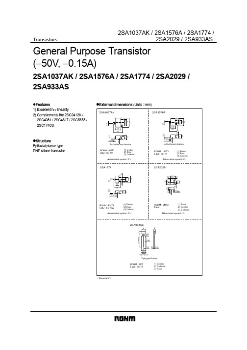
Transistors2SA2029 / 2SA933AS General Purpose Transistor(−50V, −0.15A)2SA1037AK / 2SA1576A / 2SA1774 / 2SA2029 /2SA933AS!Features1) Excellent h FE linearity.2) Complements the 2SC2412K /2SC4081 / 2SC4617 / 2SC5658 / 2SC1740S.!StructureEpitaxial planar type.PNP silicon transistor !External dimensions (Units : mm)∗ Denotes h FETransistors 2SA2029 / 2SA933AS!Absolute maximum ratings (T a=25°C)Collector-base voltage Collector-emitter voltage Emitter-base voltage Collector currentCollector powerdissipationJunction temperature Storage temperatureParameterV CBO V CEO V EBO I CP C Tj Tstg−60V V V A (DC)˚C ˚C−50−6−0.15W0.20.150.32SA1037AK, 2SA1576A2SA2029, 2SA17742SA933AS 150−55~+150Symbol Limits Unit !Electrical characteristics (T a=25°C)Collector-base breakdown voltage Collector-emitter breakdown voltage Emitter-base breakdown voltage Collector cutoff current Emitter cutoff currentDC current transfer ratio Collector-emitter saturation voltage Transition frequency Output capacitanceParameterSymbol BV CBO BV CEO BV EBO I CBO I EBO h FE V CE(sat)f T CobMin.−60−50−6−−120−−−−−−−−−−1404.0−−−−0.1−0.1560−0.5−5.0V I C=−50µA I C =−1µA I E =−50µA V CB =−60V V EB =−6VV CE =−6V, I C =−1mAI C /I B =−50mA/−5mA V CE =−12V, I E =2mA, f =30MHz V CB =−12V, I E =0A, f =1MHzV V µA µA −V MHz pFTyp.Max.Unit Conditions!Packaging specifications and h FEh FE values are classified as follows:Item Q R S h FE120~270180~390270~560Transistors 2SA2029 / 2SA933AS!Electrical characteristic curvesFig.1 Grounded emitter propagationcharacteristicsC O L L E C T O R C U R R E N T : I c (m A )−−−−−−−−−BASE TO EMITTER VOLTAGE : V BE (V)Fig.2 Grounded emitter outputcharacteristics (I)−−−−−C O L L E C T O R C U R R E N T : I C (m A )COLLECTOR TO MITTER VOLTAGE : V CE (V)Fig.3 Grounded emitter outputcharacteristics (II)−−−−−C O L L E C T O R C U R R E N T : I C (m A )COLLECTOR TO EMITTER VOLTAGE : V CE (V)Fig.4 DC current gain vs.collector current (I)D C C U R RE N T G A I N : h FECOLLECTOR CURRENT : I C (mA)Fig.5 DC current gain vs.collector current (II)−D C C U R RE N T G A I N : hF ECOLLECTOR CURRENT : I C (mA)Fig.6 Collector-emitter saturationvoltage vs. collector current (I)−−−−−−COLLECTOR CURRENT : I C (mA)C O L L EC T O R S A T U R A T I O N V O L T A G E : V C E (s a t ) (V )Fig.7 Collector-emitter saturationvoltage vs. collector current (II)−−−−−−COLLECTOR CURRENT : I C (mA)C O L L E C T O RS A T U R A T I O N V O L T A G E : V C E (s a t ) (V )Fig.8 Gain bandwidth product vs.emitter currentEMITTER CURRENT : I E (mA)T R A N S I T I O N F R E Q U E N C Y : f T (M H z )Fig.9 Collector output capacitance vs.collector-base voltageEmitter inputcapacitance vs.emitter-base voltageCOLLECTOR TO BASE VOLTAGE : V CB (V)EMITTER TO BASE VOLTAGE : V EB (V)C O L L E C T O R O U T P U T C A P A C I T A N C E :C o b (p F )E M I T T E R I N P U T C A P A C I T A N C E : C i b (p F )。
2SA673三极管参数 TO-92三极管2SA673规格书

A,Dec,20102. COLLECTORJIANGSU CHANGJIANG ELECTRONICS TECHNOLOGY CO., LTDTO-92 Plastic-Encapsulate Transistors2SA673 TRANSISTOR (PNP)FEATURESz Low Frequency Amplifierz Complementary Pair with 2SC1213MAXIMUM RATINGS (T a =25℃ unless otherwise noted)ELECTRICAL CHARACTERISTICS (T a =25℃ unless otherwise specified)ParameterSymbol Test conditions Min Typ Max Unit Collector-base breakdown voltage V (BR)CBO I C =-0.01mA,I E =0 -35 V Collector-emitter breakdown voltage V (BR)CEOI C =-1mA,I B =0 -35V Emitter-base breakdown voltage V (BR)EBOI E =-0.01mA,I C =0 -4VCollector cut-off current I CBO V CB =-20V,I E =0 -0.5 μA Emitter cut-off current I EBO V EB =-3V,I C =0 -0.5 μA h FE(1) V CE =-3V, I C =-10mA 60 320 DC current gainh FE(2)*V CE =-3V, I C =-500mA 10Collector-emitter saturation voltage V CE(sat)* I C =-150mA,I B =-15mA -0.6 VBase-emitter voltageV BEV CE =-3V, I C =-10mA-0.75V*Pulse test: pulse width ≤300μs, duty cycle ≤ 2.0%.CLASSIFICATION OF h FE(1)RANK B C DRANGE60-120 100-200 160-320Symbol Parameter Value Unit V CBO Collector-Base Voltage -35 V V CEO Collector-Emitter Voltage -35 V V EBO Emitter-Base Voltage -4 V I C Collector Current-0.5 A P C Collector Power Dissipation400 mW R θJA Thermal Resistance From Junction To Ambient 312 ℃/W T j Junction Temperature 150 ℃ T stgStorage Temperature-55~+150℃【南京南山半导体有限公司 — 长电三极管选型资料】 【南京南山半导体有限公司 — 长电三极管选型资料】 【南京南山半导体有限公司 — 长电三极管选型资料】Sponge strip2000 pcsSponge strip The top gasketLabel on the Inner BoxPlastic bagLabel on the Outer BoxInner Box: 333 mm ×162mm ×43mmOuter Box: 350 mm × 340mm × 250mmQA LabelSeal the box with the tapeStamp “EMPTY” on the empty boxInner Box: 240 mm ×165mm ×95mmLabel on the Inner BoxOuter Box: 525 mm × 360mm × 262mmLabel on the Outer BoxQA LabelSeal the box with the tapeStamp “EMPTY” on the empty box。
2SB系列晶体管参数
结构 PNP PNP PNP PNP PNP PNP PNP PNP PNP PNP PNP PNP PNP PNP PNP PNP PNP PNP PNP PNP PNP PNP PNP PNP PNP PNP PNP PNP PNP PNP PNP PNP PNP PNP PNP PNP PNP PNP PNP PNP PNP PNP PNP PNP PNP PNP PNP PNP PNP PNP PNP PNP PNP
松下 松下 松下 松下 日立 松下 松下 松下 松下 日电
日电 日电 日电 日电 日电 日电 日电 三洋 日电 日电 三洋 三洋 三洋 松下 罗姆 罗姆 三洋 三洋 三洋 三洋 日立 东芝 东芝 松下 日电 日电 富士电机 富士电机 罗姆 罗姆 日立 日立 日立 日立 日立 日立 富士电机 东芝 三洋 松下 松下 松下 日立 三洋
vcbo(V) -60 -50 -110 -60 -60 -35 -130 -130 -25 -200 -200 -100 -100 -100 -220 -70 -180 -20 -100 -25 -25 -30 -70 -70 -100 -80 -25 -100 -500 -60 -30 -60 -30 -100 -120 -25 -35 -100 -50 -100 -100 -60 -30 -60 -120 -120 -120 -120 -180 -180 -180 -180 -100
2SJ103_07中文资料

4
2007-11-01
Absolute Maximum Ratings (Ta = 25°C)
Characteristics
Symbol
Rating
UnitΒιβλιοθήκη Gate-drain voltage Gate current Drain power dissipation Junction temperature Storage temperature range
2SJ103
3
2007-11-01
元器件交易网
2SJ103
RESTRICTIONS ON PRODUCT USE
• The information contained herein is subject to change without notice.
20070701-EN GENERAL
JEDEC
TO-92
temperature, etc.) may cause this product to decrease in the
JEITA
SC-43
reliability significantly even if the operating conditions (i.e. operating temperature/current/voltage, etc.) are within the
TOSHIBA
2-5F1C
absolute maximum ratings. Please design the appropriate reliability upon reviewing the
Weight: 0.21 g (typ.)
Toshiba Semiconductor Reliability Handbook (“Handling