6_Decoupling Capacitance
MicroPHYTM MII Evaluation Board DEMO BOARD MANUAL

78Q2123-DB78Q2133-DB78Q21x3-DB MicroPHY TMMII Evaluation BoardDEMO BOARD MANUALFebruary 2006DESCRIPTIONThe 78Q21x3-DB is a design example for a 10/100BASE-TX Mbit/second Fast Ethernet MII Interface adaptor. A 78Q2123 or 78Q2133 MicroPHY transceiver from Teridian provides the network physical interface and MII (Medium Independent Interface) interface.Teridian Semiconductor’s MicroPHY is an auto-sensing, auto-switching 10/100BASE-TX Fast Ethernet transceiver with full duplex operation capability. The device interfaces directly to the IEEE-802.3u MII port. Full-featured MII management functions are included along with an extended register set. The MicroPHY five bit PHY address is defaulted to 0x001. The MicroPHY interfaces to CAT5 UTP cable via a 1:1 transformer. The transceiver’s transmitter includes on-chip the pulse shaper and low power line driver. The receiver incorporates a sophisticated combination of real-time adaptive equalization, an adaptive DC offset adjustment circuit and baseline wander correction. Smart squelch circuitry further improves the receiver’s noise rejection. Full featured auto-negotiation or parallel detect modes are supported. The demo board requires operation with a +3.3V power supply.Design Kit contains:√ MicroPHY MII Demo Board √ Demo Board Parts List √ P.C.B. Gerber Files √ Demo Board schematic √ MicroPHY Data Sheet 10/100Base-TX InterfaceRJ45 Pin Assignment Pin Signal Pin Signal 1 TX+ 5 N/C 2 TX- 6 RX- 3 RX+ 7 N/C 4 N/C 8 N/CMII: Medium Independent InterfacePin Assignment: (40 Pin Male Subminiature D, 0.050) Pin Signal Pin Signal 1 +3.3V 21 +3.3V 2 MDIO 22 COMMON 3 MDC 23 COMMON 4 RXD3 24 COMMON 5 RXD2 25 COMMON 6 RXD1 26 COMMON 7 RXD0 27 COMMON 8 RXDV 28 COMMON 9 RXCLK 29 COMMON 10 RXER 30 COMMON 11 TXER 31 COMMON 12 TXCLK 32 COMMON 13 TXEN 33 COMMON 14 TXD0 34 COMMON 15 TXD1 35 COMMON 16 TXD2 36 COMMON 17 TXD3 37 COMMON 18 COL 38 COMMON 19 CRS 39 COMMON 20 +3.3V 40 +3.3VOrdering Number Description78Q21x3-DBMicroPHY MII Demo BoardMII ADAPTOR WITH MICROPHYUse With the Netcom Smart-BitsThe Netcom expects to be the master and defaults to 100BASE-TX Half-Duplex operation. Fast-Ether Windows may require the reconfiguration of the MicroPHY’s control register MR0 bits for similar operation. The MicroPHY defaults to auto-negotiate with full capabilities.After initialization the MicroPHY defaults to 100BASE-TX Full-Duplex operation. When connected to another fully capable transceiver the transceivers will be in full-duplex mode. The default configuration of the Netcom is 100BASE-TX Half-Duplex operation. If data transfers were to commence, the Netcom would display Collision errors (because it does not automatically read the transceivers and reconfigure).The default MII PHY address for the MicroPHY is 0x001. Additionally, the MicroPHY will respond to the broadcast address 0x000.If a transceiver is used which defaults to 100BASE-TX Half-Duplex operation, the MicroPHY will adjust itself for half-duplex operation (assuming the MicroPHY is setup for the proper technologies).To establish proper operation between the MicroPHY and the Netcom, click on the “Options” button followed by selecting “Full Duplex MII”. Repeat selecting “Full Duplex MII” twice to ensure that everything is configured identically.The MicroPHY can be configured for half-duplex operation to minimize incompatibilities with other transceivers and the Netcom.10/100Mbps Transformer SelectionThe line interface for the MicroPHY requires a pair of 1:1 isolation transformers. Integrated common-mode chokes are recommended for satisfying FCC radiated EMI requirements. Additional filtering is not required with the MicroPHY due to internal waveform shaping circuitry. The line transformer characteristics are outlined below:ConditionName ValueTurns Ratio 1 CT : 1 CT@ 10 mV, 10 kHzOpen-Circuit Inductance 350 µH (min)See Note 1.Leakage Inductance 0.40 µH (max) @ 1 MHz (min)Inter-Winding Capacitance 25 pF (max)D.C. Resistance 0.9 ohm (max)Insertion Loss 1.1 dB (typ) 0 - 100 MHzVrmsHIPOT 1500Note 1: The receive line transformer’s Open-Circuit Inductance can be as low as 100 µH for the MicroPHY. The MicroPHY incorporates baseline wander correction circuitry, which allows the receiver to track the incoming data signal when there is excessive transformer droop.For Commercial Temperature (0°C ~ 70°C)Teridian Semiconductor has performed line testing with the following transformers and found their performance acceptable with the MicroPHY:Manufacturer Part NumberTDKTLA-6T103Bel-Fuse S558-5999-46TG22-3506NDHaloPE-68515PulseST6118Valor20PMT04YCLThe following transformers are low profile packages (0.100 in/2.5 mm or less).TLA-6T118TDKTG110-S050HaloEPF8023GPCAThe following devices integrate the transformers with the RJ45 connector.TDKTLA-6T704RJS-1A08T089ADeltaThe following devices integrate the transformers, RJ45 connector, LEDs and termination resistors.J0011D21B/EPulseThe above evaluations were performed using Netcom’s Smart-Bits Fast Ethernet Analyzer. The Teridian Semiconductor MicroPHY MII Adapter and Lancast Fast Ethernet Adapter were attached to the Netcom’s Ports A & B respectively. Twisted pair Category 5 General Cable P/N 459360 was used to connect the two transceivers. 100 Mbps performance was measured using cable lengths of both 12 inches and 115 meters. 10 Mbps performance was evaluated using 100 meters of Category 3 cable.The Netcom was configured to use the Baseline Wander Packet file. Packet length was 1500 bytes.All transformers listed above met or exceeded IEEE’s 802.3 Bit Error Rate requirements of 10-8.For Industrial Temperature (-40°C ~ +85°C)Now most of the transformer vendors also offer industrial temp transformer, which will work with the 78Q2133. Here is the recommended industrial temp transformer list:Manufacturer Part NumberBelfuse S558-5999-U5HX1148PulseTG110-E050N5HaloPCB Layout ConsiderationsThe following recommendations enhance the MicroPHY’s performance while minimizing EMC emissions:1. The transformer to transceiver signal traces must be 100Ω differential transmission lines.2. Place the termination network components near the input data pins of the transceiver or transformer.3. Make all differential signal pairs short and of the same length.4. Decouple the transceiver thoroughly with 0.01µF and 0.1µF capacitors.5. Locate these decoupling capacitors as close as possible to the respective transceiver VCC and GNDpins.6. All decoupling capacitor and transceiver VCC and GND connections should tie immediately to a VCC orGND plane via with minimum trace inductance.7. Total decoupling capacitance should be greater than the load capacitance that the digital output driversmust drive.8. Use low inductance, ceramic surface mount decoupling capacitors.9. Use a multi-layer PCB with the inner layers dedicated to GND and VCC.10. A single VCC and GND plane is recommended for optimum performance. The lowest possible seriesimpedance is required between the analog and digital VCC and GND pins respectively of the transceiver.11. The outer layers of a 4 layer PCB are to be used for signal routing.12. Place the highest speed signals on the layer adjacent to the GND plane.13. Physically separate the analog signals from the digital signals by placing them on opposite layers orrouting them away from each other.14. Additional component and solder side ground layers may be added for maximum EMC containment.15. The GND plane should extend out to the transceiver side of the transformer. Remove the VCC and GNDplanes from the line side of the transformer to the RJ-45 connector.16. Do not allow the chassis ground plane to cross over the transceiver GND plane. Minimum separationmust accommodate over 1.5kV.17. Provide onboard termination of the unused signal pairs in the CAT-5 cable.18. Use a shielded RJ-45 connector with its case stakes soldered to the chassis ground.19. Locate the transformer adjacent to the RJ-45 to minimize the shunt capacitance to the line.20. Minimize RF current fringing by making the VCC plane 0.10 inch smaller than the GND plane. If multipletransceivers are used, provide partitions in the VCC and GND planes between the analog sections.Maintain the partition from the transformer up to the transceiver’s analog interface. Do not cross thesepartitions with signal traces, in particular any digital signals from adjacent transceivers.21. Add series resistors on all transceiver MII outputs to minimize digital output driver peak currents.22. Minimize the use of vias when routing the analog signal traces.23. Isolate the crystal and its capacitors from the analog signals with a guard ring.24. The crystal compensation capacitor value (C2 & C3) must be selected to trim the oscillator’s frequency to25.0000 MHz ±50ppm. The optimum value will be layout dependent. A mere ±4pF can shift the 25MHz±100Hz. The 25.0000 MHz ±50ppm is specified by the IEEE.Note: System vendors need to select the proper crystal according to their applications, such as operating environment, product lifetime, and etc since crystal aging, operating temperature, and other factors can affect the crystal frequency tolerance.MicroPHY MII Demo Board Parts ListQ T Y R EF ER E N C E N U M B E R D E S C R I P T I O N PA R T N U M B E R PA C KA G E MA N U FA C T U R E R1 U1 IC, 10/100Mbps LANTransceiverTSC 78Q2123 QFN32 TSC1 J2 RJ45, XFRM, LED,10BaseT/100BaseTX J0011D21Bwith LEDsPULSETLA-6T704without LEDsTDK1 Q1 CRYSTAL, 25.000MHZ ECCM1-25.000MHZ ECCM1 ECLIPTEK2 D1,D2 LED, Optional LU20125 R/A LUMEX7 R5,R6,R7,R8,R11,R12,R13,R14,R23,R25RES, 100 CC06032 R1,R2 RES, 680, Optional CC06033 R3,R4,R26 RES, 5.1K CC06031 R27 RES, 10K CC06034 R9,R10,R21,R22 RES, 49.9, 1% CC06034 C14,C15,C16,C17 CAP, CER, 10PF, Optional CC06032 C2,C3 CAP, CER, 27PF CC06033 C4,C12,C13 CAP, CER, 0.01UF CC060310 C6,C7,C8,C10,C11 CAP, CER, 0.1UF C1608Y51H104Z CC0603 TDK1 C9 CAP, CER, 10UF CC08051 P1 CONN, MALE, 40 PIN FCN-238P040-G/F FUJITSU1 P.C.B.Top SilkscreenTop LayerVCC LayerGround LayerBottom LayerNo responsibility is assumed by Teridian Semiconductor Corporation for use of this product or for any infringements of patents and trademarks or other rights of third parties resulting from its use. No license is granted under any patents, patent rights or trademarks of Teridian Semiconductor Corporation, and the company reserves the right to make changes in specifications at any time without notice. Accordingly, the reader is cautioned to verify that the data sheet is current before placing orders.Teridian Semiconductor Corporation, 6440 Oak Canyon, Irvine, CA 92618-5201TEL: (714) 508-8800, FAX: (714) 508-887778Q2123-DB78Q2133-DB。
ICS501 LOCO PLL时钟乘法器数据表说明书
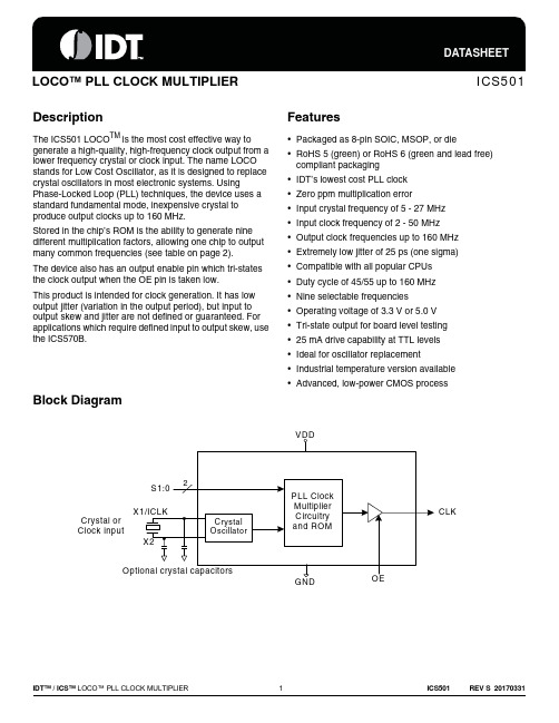
DescriptionThe ICS501 LOCO TM is the most cost effective way to generate a high-quality, high-frequency clock output from a lower frequency crystal or clock input. The name LOCO stands for Low Cost Oscillator, as it is designed to replace crystal oscillators in most electronic systems. Using Phase-Locked Loop (PLL) techniques, the device uses a standard fundamental mode, inexpensive crystal to produce output clocks up to 160 MHz.Stored in the chip’s ROM is the ability to generate nine different multiplication factors, allowing one chip to output many common frequencies (see table on page 2).The device also has an output enable pin which tri-states the clock output when the OE pin is taken low.This product is intended for clock generation. It has low output jitter (variation in the output period), but input to output skew and jitter are not defined or guaranteed. For applications which require defined input to output skew, use the ICS570B.Features•Packaged as 8-pin SOIC, MSOP, or die •RoHS 5 (green) or RoHS 6 (green and lead free) compliant packaging•IDT’s lowest cost PLL clock•Zero ppm multiplication error•Input crystal frequency of 5 - 27 MHz•Input clock frequency of 2 - 50 MHz•Output clock frequencies up to 160 MHz •Extremely low jitter of 25 ps (one sigma)•Compatible with all popular CPUs•Duty cycle of 45/55 up to 160 MHz•Nine selectable frequencies•Operating voltage of 3.3 V or 5.0 V•Tri-state output for board level testing•25 mA drive capability at TTL levels•Ideal for oscillator replacement•Industrial temperature version available •Advanced, low-power CMOS processBlock DiagramPin Assignment Clock Output Table0 = connect directly to ground 1 = connect directly to VDD M = leave unconnected (floating)Common Output Frequency Examples (MHz)Pin DescriptionsS1S0CLK Minimum Input 004X input per page 50M 5.3125X input 20 MHz 015X input per page 5M 0 6.25X input 4 MHz M M 2X input per page 5M 1 3.125X input 8 MHz 106X input per page 51M 3X input per page 5118X inputper page 5Output 2024303233.3337.54048506062.5Input1012101616.6612101216.661020Selection (S1, S0)M, M M, M 1, M M, M M, M M, 10, 00, 01, M 1, 0M, 1Output 6466.6672758083.3390100106.25120125Input1616.6612121016.661520201520Selection (S1, S0)0, 00, 01, 0M, 01, 10, 11, 00, 10, M1, 1M, 0PinNumberPin NamePin TypePin Description1XI/ICLK Input Crystal connection or clock input.2VDD Power Connect to +3.3 V or +5 V.3GND Power Connect to ground.4S1Tri-level IinputSelect 1 for output clock. Connect to GND or VDD or float.5CLK Output Clock output per table above.6S0Tri-level InputSelect 0 for output clock. Connect to GND or VDD or float.7OE Input Output enable. Tri-states CLK output when low. Internal pull-up.8X2OutputCrystal connection. Leave unconnected for clock input.External ComponentsDecoupling CapacitorAs with any high-performance mixed-signal IC, the ICS501 must be isolated from system power supply noise to perform optimally.A decoupling capacitor of 0.01µF must be connectedbetween VDD and the GND. It must be connected close to the ICS501 to minimize lead inductance. No external power supply filtering is required for the ICS501.Series Termination ResistorA 33Ω terminating resistor can be used next to the CLK pin for trace lengths over one inch.Crystal Load CapacitorsThe total on-chip capacitance is approximately 12 pF. A parallel resonant, fundamental mode crystal should be used. The device crystal connections should include pads for small capacitors from X1 to ground and from X2 to ground. These capacitors are used to adjust the stray capacitance of the board to match the nominally required crystal load capacitance. Because load capacitance can only be increased in this trimming process, it is important to keep stray capacitance to a minimum by using very short PCB traces (and no vias) between the crystal and device. Crystal capacitors, if needed, must be connected from each of the pins X1 and X2 to ground.The value (in pF) of these crystal caps should equal (C L -12 pF)*2. In this equation, C L = crystal load capacitance in pF. Example: For a crystal with a 16 pF load capacitance, each crystal capacitor would be 8 pF [(16-12) x 2 = 8].Absolute Maximum RatingsStresses above the ratings listed below can cause permanent damage to the ICS501. These ratings, which are standard values for IDT commercially rated parts, are stress ratings only. Functional operation of the device at these or any other conditions above those indicated in the operational sections of the specifications is not implied. Exposure to absolute maximum rating conditions for extended periods can affect product reliability. Electrical parameters are guaranteed only over the recommended operating temperature range.Recommended Operation ConditionsItemRatingSupply Voltage, VDD 7 VAll Inputs and Outputs-0.5 V to VDD+0.5 V Ambient Operating Temperature -40 to +85︒C Storage Temperature -65 to +150︒C Soldering Temperature260︒CParameterMin.Typ.Max.UnitsAmbient Operating Temperature (commercial)0+70︒C Ambient Operating Temperature (industrial)-4085︒C Power Supply Voltage (measured in respect to GND)+3.0+5.25VDC Electrical CharacteristicsVDD=5.0 V ±5%, Ambient temperature -40 to +85︒C, unless stated otherwiseParameter Symbol Conditions Min.Typ.Max.Units Operating Voltage VDD 3.0 5.25VInput High Voltage, ICLK only V IH ICLK (pin 1)(VDD/2)+1VInput Low Voltage, ICLK only V IL ICLK (pin 1)(VDD/2)-1VInput High Voltage V IH OE (pin 7) 2.0VInput Low Voltage V IL OE (pin 7)0.8VInput High Voltage V IH S0, S1VDD-0.5VInput Low Voltage V IL S0, S10.5VOutput High Voltage V OH I OH = -25 mA 2.4VOutput Low Voltage V OL I OL = 25 mA0.4VIDD Operating Supply Current, 20 No load, 100M20mA Short Circuit Current CLK output+70mA On-Chip Pull-up Resistor Pin 7270kΩInput Capacitance, S1, S0, and OE Pins 4, 6, 74pF Nominal Output Impedance20ΩAC Electrical CharacteristicsVDD = 5.0 V ±5%, Ambient Temperature -40 to +85︒ C, unless stated otherwiseNote 1: Measured with 15 pF load.Thermal Characteristics for 8SOICThermal Characteristics for 8MSOPParameterSymbolConditions Min.Typ.Max.UnitsInput Frequency, crystal input F IN 527MHz Input Frequency, clock inputF IN 250MHz Output Frequency, VDD = 4.75 to 5.25 V F OUT 0︒C to +70︒C 13160MHz -40︒C to +85︒C 13140 MHzOutput Frequency, VDD = 3.0 to 3.6 V F OUT 0︒C to +70︒C 13100MHz -40︒C to +85︒C 1390MHz Output Clock Rise Time t OR 0.8 to 2.0 V, Note 11ns Output Clock Fall Time t OF 2.0 to 8.0 V, Note 11nsOutput Clock Duty Cycle t OD1.5 V, up to 160 MHz4549-5155%PLL Bandwidth10kHzOutput Enable Time, OE high to outputon50ns Output Disable Time, OE low to tri-state 50ns Absolute Clock Period Jitter t ja Deviation from mean+70ps One Sigma Clock Period Jitter t js25psParameterSymbolConditionsMin.Typ.Max.UnitsThermal Resistance Junction to AmbientθJA Still air 150︒C/W θJA 1 m/s air flow 140︒C/W θJA 3 m/s air flow 120︒C/W Thermal Resistance Junction to Case θJC 40︒C/W Thermal Resistance Junction to Top of CaseψJTStill air20︒C/WParameterSymbolConditionsMin.Typ.Max.UnitsThermal Resistance Junction to AmbientθJA Still air95︒C/W Thermal Resistance Junction to CaseθJC48︒C/WPackage Outline and Package Dimensions (8-pin MSOP, 3.00 mm Body) Package dimensions are kept current with JEDEC Publication No. 95Package Outline and Package Dimensions (8-pin SOIC, 150 Mil. Narrow Body) Package dimensions are kept current with JEDEC Publication No. 95Ordering InformationPart / Order Number Marking Shipping Packaging Package Temperature 501MLF501MLF Tubes8-pin SOIC0 to +70︒ C501MLFT501MLF Tape and Reel8-pin SOIC0 to +70︒ C501MILF501MILF Tubes8-pin SOIC-40 to +85︒ C501MILFT501MILF Tape and Reel8-pin SOIC-40 to +85︒ C501GLF01GL Tubes8-pin MSOP0 to +70︒ C501GLFT01GL Tape and Reel8-pin MSOP0 to +70︒ C501GILF1GIL Tubes8-pin MSOP-40 to +85︒ C501GILFT1GIL Tape and Reel8-pin MSOP-40 to +85︒ C501-DWF-Die on uncut, probed wafers0 to +70︒ C501-DPK-Tested die in waffle pack0 to +70︒ C501E-DPK-Tested die in waffle pack0 to +70︒ C"LF" suffix to the part number are the Pb-Free configuration and are RoHS compliant.While the information presented herein has been checked for both accuracy and reliability, Integrated Device Technology (IDT) assumes no responsibility for either its use or for the infringement of any patents or other rights of third parties, which would result from its use. No other circuits, patents, or licenses are implied. This product is intended for use in normal commercial applications. Any other applications such as those requiring extended temperature range, high reliability, or other extraordinary environmental requirements are not recommended without additional processing by IDT. IDT reserves the right to change any circuitry or specifications without notice. IDT does not authorize or warrant any IDT product for use in life support devices or critical medical instruments.DISCLAIMER Integrated Device Technology, Inc. (IDT) and its affiliated companies (herein referred to as “IDT”) reserve the right to modify the products and/or specifications described herein at any time, without notice, at IDT’s sole discretion. Performance specifications and operating parameters of the described products are determined in an independent state and are not guaranteed to perform the same way when installed in customer products. The information contained herein is provided without representation or warranty of any kind, whether express or implied, including, but not limited to, the suitability of IDT's products for any particular purpose, an implied warranty of merchantability, or non-infringement of the intellectual property rights of others. This document is presented only as a guide and does not convey any license under intellectual property rights of IDT or any third parties.IDT's products are not intended for use in applications involving extreme environmental conditions or in life support systems or similar devices where the failure or malfunction of an IDT product can be reasonably expected to significantly affect the health or safety of users. Anyone using an IDT product in such a manner does so at their own risk, absent an express, written agreement by IDT.Corporate HeadquartersIntegrated Device Technology, For Sales800-345-7015408-284-8200Fax: 408-284-2775For Tech Support/go/supportInnovate with IDT and accelerate your future networks. Contact:。
zbc埋入式电容的英文单词
zbc埋入式电容的英文单词The English word for "zbc埋入式电容" is "embedded capacitor".Embedded capacitors, also known as buried capacitors, are an essential component in modern electronic devices and circuits. They are designed to provide capacitance within the circuit board itself, eliminating the need for discrete capacitors. This integration not only saves space but also improves the overall performance and reliability of the electronic system.The concept of embedded capacitors involves incorporating a layer of dielectric material with a high dielectric constant into the printed circuit board (PCB) itself. This dielectric layer acts as a capacitor, capable of storing and releasing electrical energy. The dielectric material used in embedded capacitors is typically a high-performance polymer or ceramic with excellent electrical properties.One of the main advantages of embedded capacitors is their ability to minimize the parasitic inductance and resistance associated with discrete capacitors. In traditional PCB designs, the leads and traces connecting the capacitors introduce parasitic elements that can degrade the performance of the circuit. By integrating the capacitor directly into the PCB, these parasitic elements are significantly reduced, leading to improved signal integrity and faster response times.Embedded capacitors also offer enhanced thermal management capabilities. By distributing the capacitors throughout the PCB, heat generated during operation can be dissipated more efficiently. This reduces the risk of overheating and improves the overall reliability of the electronic device.Furthermore, the integration of capacitors into the PCB simplifies the assembly process and reduces manufacturing costs. The need for manual placement of discrete capacitors is eliminated, saving time and reducing the risk of human error. Additionally, the smaller form factor of embedded capacitors allows for higher-density circuit designs, further optimizing the use of available space on the PCB.The application of embedded capacitors is widespread across various industries, including telecommunications, automotive, aerospace, and consumer electronics. They are commonly used in power management circuits, high-frequency filters, decoupling networks, and signal conditioning circuits. The demand for embedded capacitors continues to grow as electronic devices become more compact and require higher performance levels.In conclusion, "zbc埋入式电容" translates to "embedded capacitor" in English. Embedded capacitors offer numerous benefits, including improved circuit performance, enhanced thermal management, reduced manufacturing costs, and increased design flexibility. As electronic devices continue to evolve, embedded capacitors play a crucial role in enabling smaller, more efficient, and reliable systems.。
IR压降(IR-Drop)

IR压降(IR-Drop)IR压降是指出现在集成电路中电源和地网络上电压下降或升高的一种现象。
随着半导体工艺的演进金属互连线的宽度越来越窄,导致它的电阻值上升,所以在整个芯片范围内将存在一定的IR压降。
IR压降的大小决定于从电源PAD到所计算的逻辑门单元之间的等效电阻的大小。
SoC设计中的每一个逻辑门单元的电流都会对设计中的其它逻辑门单元造成不同程度的IR压降。
如果连接到金属连线上的逻辑门单元同时有翻转动作,那么因此而导致的IR压降将会很大。
然而,设计中的某些部分的同时翻转又是非常重要的,例如时钟网络和它所驱动的寄存器,在一个同步设计中它们必须同时翻转。
因此,一定程度的IR压降是不可避免的。
IR压降可能是局部或全局性的。
当相邻位置一定数量的逻辑门单元同时有逻辑翻转动作时,就引起局部IR压降现象,而电源网格某一特定部分的电阻值特别高时,例如R14远远超出预计时,也会导致局部IR压降;当芯片某一区域内的逻辑动作导致其它区域的IR压降时,称之为全局现象。
IR压降问题的表现常常类似一些时序甚至可能是信号的完整性问题。
如果芯片的全局IR压降过高,则逻辑门就有功能故障,使芯片彻底失效,尽管逻辑仿真显示设计是正确的。
而局部IR压降比较敏感,它只在一些特定的条件下才可能发生,例如所有的总线数据同步进行翻转,因此芯片会间歇性的表现出一些功能故障。
而IR压降比较普遍的影响就是降低了芯片的速度。
试验表明,逻辑门单元上5%的IR压降将使正常的门速度降低15%。
天线效应0.4um以上的工艺,我们一般不大会考虑天线效应。
而采用0.4um以下的工艺就不得不考虑这个问题了。
Normally the first way to fix antenna effect is changing metal layers. Insering diode is thelast way. P&R tools can handle this automatically.其实foundry提供的PAE ratio,只是一个经验值,是留了很大的margin的。
IRdrop_AntennaEffect_EM电迁移
IR drop的兄弟,EM现象
EM是电子迁移现象. 作为特定的工艺来说,某个金属层会有一个最大电流密度,在这层金属上允许的最大电流密度是有一定限度的,过大的电流会造成金属断裂. 电流经过金属层时,电子和原子可能会碰撞,电流过大这种碰撞会产生热效应,同时热效应会加剧原子和电子的碰撞. 某种意义上来说,EM效应也有热效应的影子.这种大电流的情况下,不仅仅是电子的移动,有可能会在金属层造成阳极原子的迁移,这种迁移造成了金属连线的破损断裂,同时也可能会顺着迁移方向短路到其他线路
1。性能(performance) 由管子的Tdelay=c/u可知,电压降低,门的开关速度越慢,性能越差。
2。功能(function) 实际上在极端的情况下甚至功能也会受影响的。在深亚微米下,如果Power/Ground network做的也很差,然后碰上了很不好的case,IR drop会很大,如果用的是high Vt的process,则DC noise margin就比较小了。这样就有可能功能错误。
.
IR drop 的分析
对芯片电源进行有效的设计必须理解IR drop的产生原理. 静态IR drop和动态IR drop之间没有什么必然的联系. 现在的芯片设计中,电源设计和IR drop分析被不断的前提,应为深亚微米之后的电源压降现象更严重,早日分析早日发现问题并在设计中考虑到是很有必要的.在后端设计中,布局之时就应该考虑电源的规划,快速布局之后就应该对电源设计做一次分析. 到Sign-off阶段再做更详细的分析:功耗\压降\电子迁移\热.
电感电阻电容 串并联 功率因数
电感电阻电容串并联功率因数英文回答:Inductance, resistance, and capacitance are fundamental concepts in electrical engineering. They are commonly used in electronic circuits and have different properties and applications.Inductance refers to the property of a component to store energy in a magnetic field. It is represented by the symbol L and is measured in henries (H). An inductor, also known as a coil or choke, is a passive electronic component that stores energy in its magnetic field when current flows through it. Inductors are used in various applications such as filtering, energy storage, and inductance-based sensors.Resistance, on the other hand, is the property of a component to oppose the flow of electric current. It is represented by the symbol R and is measured in ohms (Ω). A resistor is a passive electronic component that limits theflow of current in a circuit. It is commonly used tocontrol the amount of current or voltage in a circuit and to dissipate heat. Resistors are used in various applications such as voltage dividers, current limiting, and signal conditioning.Capacitance refers to the ability of a component to store electrical energy in an electric field. It is represented by the symbol C and is measured in farads (F).A capacitor is a passive electronic component that stores and releases electrical energy. It is commonly used in circuits for energy storage, filtering, and timing. Capacitors are used in various applications such as power supply decoupling, signal coupling, and energy storage.When it comes to series and parallel connections of inductance, resistance, and capacitance, their properties and behaviors change.In a series connection, the total inductance, resistance, or capacitance is the sum of the individual components. For example, if we have two inductors connectedin series, their total inductance is the sum of their individual inductances. Similarly, if we have two resistors connected in series, their total resistance is the sum of their individual resistances. In the case of capacitors, the total capacitance is the reciprocal of the sum of the reciprocals of the individual capacitances.In a parallel connection, the total inductance, resistance, or capacitance is calculated differently. For inductors, the total inductance is the reciprocal of the sum of the reciprocals of the individual inductances. For resistors, the total resistance is the reciprocal of the sum of the reciprocals of the individual resistances. And for capacitors, the total capacitance is the sum of the individual capacitances.Now, let's talk about power factor. Power factor is a measure of how effectively electrical power is being used in a circuit. It is the ratio of the real power (in watts) to the apparent power (in volt-amperes). A power factor of 1 means that the circuit is purely resistive and all the power is being used effectively. A power factor less than 1means that the circuit has reactive components (inductanceor capacitance) and the power is not being used efficiently.A low power factor is undesirable because it leads to inefficient power usage, increased energy costs, and can cause problems in the electrical distribution system. Power factor correction techniques are used to improve powerfactor and increase energy efficiency.中文回答:电感、电阻和电容是电气工程中的基本概念。
RT9184A型号的双通道CMOS低功耗电源管理器说明书

1DS9184A-09 April 2011Featuresz Low Quiescent Current (Typically 440μA)z Guaranteed 500mA Output Currentz Low Dropout Voltage : 600mV at 500mAz Wide Operating Voltage Ranges : 2.8V to 5.5V z Ultra-Fast Transient Response z Tight Load and Line Regulation z Current Limiting Protection z Thermal Shutdown ProtectionzOnly low-ESR Ceramic Capacitors Required for Stabilityz Custom Voltage AvailablezRoHS Compliant and 100% Lead (Pb)-FreePin ConfigurationsApplicationsz CD/DVD-ROM, CD/RWz Wireless LAN Card/Keyboard/Mouse z Battery-Powered Equipment zXDSL RouterDual, Ultra-Fast Transient Response, 500mA LDO RegulatorOrdering InformationGeneral DescriptionThe RT9184A series are an efficient, precise dual-channel CMOS LDO regulator optimized for ultra-low-quiescent applications. Both regulator outputs are capable of sourcing 500mA of output current.The RT9184A's performance is optimized for CD/DVD-ROM,CD/RW or wireless communication supply applications.The RT9184A regulators are stable with output capacitors as low as 1μF. The other features include ultra low dropout voltage, high output accuracy, current limiting protection,and high ripple rejection ratio.The RT9184A regulators are available in fused SOP-8package. Key features include current limit, thermal shutdown, fast transient response, low dropout voltage,high output accuracy, current limiting protection, and high ripple rejection ratio.(TOP VIEW)SOP-8Note :zThe output 2 is designated to larger than or equal to output 1 in voltage code order below, i.e. V OUT2 ≥ V OUT1.For example, the part number of RT9184A-FNCS is assigned for 2.5V OUT1/3.3V OUT2, contrary to the part number of RT9184A-NFCS is opposite to the rule and doesn't exist in the system.Voltage Code for Both Outputs :2: 1.2V A: 2.0V K: 3.0V U: 4.0V 3: 1.3V B: 2.1V L: 3.1V V: 4.1V 4: 1.4V C: 2.2V M: 3.2V W: 4.2V : : : :9: 1.9V J: 2.9V T: 3.9V Z: 4.5VRichTek products are :` RoHS compliant and compatible with the current require-ments of IPC/JEDEC J-STD-020.`Suitable for use in SnPb or Pb-free soldering processes.VOUT1VIN1VOUT2VIN2GNDGND GND GND2DS9184A-09 April 2011Function Block DiagramTypical Application CircuitNote: To prevent oscillation, a 1μF minimum X7R or X5R dielectric is strongly recommended if ceramics are used as input/output capacitors. When using the Y5V dielectric,the minimum value of the input/output capacitance that can be used for stable over full operating temperature range is 3.3μF. (see Application Information Section for further details)V V OUT1V IN2V IN1VIN1VOUT1VIN2GNDVOUT23DS9184A-09 April 2011Absolute Maximum Ratings (Note 1)z Supply Input Voltage ------------------------------------------------------------------------------------------------6.5V zPower Dissipation, P D @ T A = 25°CSOP-8------------------------------------------------------------------------------------------------------------------0.625W zPackage Thermal Resistance (Note 2)SOP-8, θJA ------------------------------------------------------------------------------------------------------------160°C/W z Lead Temperature (Soldering, 10 sec.)-------------------------------------------------------------------------260°C z Junction T emperature -----------------------------------------------------------------------------------------------150°Cz Storage Temperature Range ---------------------------------------------------------------------------------------−65°C to 150°C zESD Susceptibility (Note 3)HBM (Human Body Mode)-----------------------------------------------------------------------------------------2kV MM (Machine Mode)------------------------------------------------------------------------------------------------200VElectrical CharacteristicsRecommended Operating Conditions (Note 4)z Supply Input Voltage ------------------------------------------------------------------------------------------------2.8V to 5.5V zJunction T emperature Range --------------------------------------------------------------------------------------−40°C to 125°C(V IN= V OUT + 1V, or V IN = 2.8V whichever is greater, C IN = 1μF, C OUT = 1μF, T A = 25°C , for each LDO unless otherwise specified)4DS9184A-09 April 2011 Note 1. Stresses listed as the above “Absolute Maximum Ratings ” may cause permanent damage to the device. These arefor stress ratings. Functional operation of the device at these or any other conditions beyond those indicated in the operational sections of the specifications is not implied. Exposure to absolute maximum rating conditions for extended periods may remain possibility to affect device reliability.Note 2. θJA is measured in the natural convection at T A = 25°C on a low effective thermal conductivity test board ofJEDEC 51-3 thermal measurement standard.Note 3. Devices are ESD sensitive. Handling precaution recommended.Note 4. The device is not guaranteed to function outside its operating conditions.Note 5. Regulation is measured at constant junction temperature by using a 20ms current pulse. Devices are tested for loadregulation in the load range from 1mA to 500mA.Note 6. The dropout voltage is defined as V IN -V OUT , which is measured when V OUT is V OUT(NORMAL) − 100mV.Note 7. Quiescent, or ground current, is the difference between input and output currents. It is defined by I Q = I IN - I OUT under noload condition (I OUT = 0mA). The total current drawn from the supply is the sum of the load current plus the ground pin current.5DS9184A-09 April 2011Typical Operating CharacteristicsOutput Voltage vs. Temperature3.23.253.33.353.4-50-25255075100125Temperature O u t p u tV o l t a g e (V )(°C)-40Quiescent Current vs. Temperature300350400450500-50-25255075100125Temperature Q u i e s c e n tC u r r e n t (u A ) (°C)-40Current Limit vs. Input Voltage70075080085090033.544.555.5Input Voltage (V)C u r r e n t L i m i t (m A )Current Limit vs. Temperature700750800850900-50-25255075100125Temperature C u r r e n t L i m i t (m A )(°C)-40Load Transient RegulationI O U T 1(100m A /D i v )V O U T 1(20m V /D i v )V O U T 2(20m V /D i v )Time (1ms/Div)V IN1 = V IN2 = 5V, C IN1 = C IN2 = 1uF(X7R)C OUT1 = C OUT2 = 1uF(X7R), I OUT2 = 0A≈≈Load Transient RegulationI O U T 2(100m A /D i v )V O U T 1(20m V /D i v )V O U T 2(20m V /D i v )Time (1ms/Div)V IN1 = V IN2 = 5V, C IN1 = C IN2 = 1uF(X7R)C OUT1 = C OUT2 = 1uF(X7R), I OUT1 = 0A≈≈≈≈6DS9184A-09 April 2011 Dropout Voltage vs. Output Current01002003004005006007008000100200300400500Output Current (mA)D r o p o u t V o l t a g e (m A )Range of Stable ESR0.010.1110100100200300400500Output Current (mA)O u t p u t Ca p a c i t o r E S R (Ω)Output NoiseO u t p u t N o i s e S i g n a l (u V )Time (1ms/Div)V IN1 = 5VI LOAD = 100mAC IN1 = 1uF C OUT1 = 1uF3042-2F = 10Hz to 100kHzLine Transient RegulationI n p u t V o l t a g eD e v i a t i o n (V )O u t p u t V ol t ag e D e v i a t i o n (m V )Time (1ms/Div)V IN1 = 3 to 4V V IN2 = 5V C IN1 = 10uF C OUT1 = 10uF3042-2Power Supply Rejection Ratio-60-50-40-30-20-100101001000100001000001000000Frequency (Hz)P S R R (d B )1k 10k 100k 1M7DS9184A-09 April 2011Application InformationLike any low-dropout regulator, the RT9184A requires input and output decoupling capacitors. The device is specifically designed for portable applications requiring minimum board space and smallest components. These capacitors must be correctly selected for good performance (see Capacitor Characteristics Section). Please note that linear regulators with a low dropout voltage have high internal loop gains which require care in guarding against oscillation caused by insufficient decoupling capacitance.Input CapacitorAn input capacitance of ≅1μF is required between the device input pin and ground directly (the amount of the capacitance may be increased without limit). The input capacitor MUST be located less than 1cm from the device to assure input stability (see PCB Layout Section). A lower ESR capacitor allows the use of less capacitance, while higher ESR type (like aluminum electrolytic) require more capacitance.Capacitor types (aluminum, ceramic and tantalum) can be mixed in parallel, but the total equivalent input capacitance/ESR must be defined as above to stable operation.There are no requirements for the ESR on the input capacitor, but tolerance and temperature coefficient must be considered when selecting the capacitor to ensure the capacitance will be ≅1μF over the entire operating temperature range.Output CapacitorThe RT9184A is designed specifically to work with very small ceramic output capacitors. The recommended minimum capacitance (temperature characteristics X7R or X5R) are 1μF to 4.7μF range with 10m Ω to 50m Ω range ceramic capacitors between each LDO output and GND for transient stability, but it may be increased without limit.Higher capacitance values help to improve transient.The output capacitor's ESR is critical because it forms a zero to provide phase lead which is required for loop stability. (When using the Y5V dielectric, the minimum value of the input/output capacitance that can be used for stable over full operating temperature range is 3.3μF.)No Load StabilityThe device will remain stable and in regulation with no external load. This is specially important in CMOS RAM keep-alive applications.Input-Output (Dropout) VoltageA regulator's minimum input-to-output voltage differential (dropout voltage) determines the lowest usable supply voltage. In battery-powered systems, this determines the useful end-of-life battery voltage. Because the device uses a PMOS, its dropout voltage is a function of drain-to-source on-resistance, R DS(ON), multiplied by the load current :V DROPOUT = V IN − V OUT = R DS(ON) × I OUT Current LimitThe RT9184A monitors and controls the PMOS' gate voltage, limiting the output current to 500mA (min.). The output can be shorted to ground for an indefinite period of time without damaging the part.Short-Circuit ProtectionThe device is short circuit protected and in the event of a peak over-current condition, the short-circuit control loop will rapidly drive the output PMOS pass element off. Once the power pass element shuts down, the control loop will rapidly cycle the output on and off until the average power dissipation causes the thermal shutdown circuit to respond to servo the on/off cycling to a lower frequency.Please refer to the section on thermal information for power dissipation calculations.Capacitor CharacteristicsIt is important to note that capacitance tolerance and variation with temperature must be taken into consideration when selecting a capacitor so that the minimum required amount of capacitance is provided over the full operating temperature range. In general, a good tantalum capacitor will show very little capacitance variation with temperature,but a ceramicmay not be as good (depending on dielectric type).Aluminum electrolytics also typically have large temperature variation of capacitance value.8DS9184A-09 April 2011 Equally important to consider is a capacitor's ESR change with temperature: this is not an issue with ceramics, as their ESR is extremely low. However, it is very important in tantalum and aluminum electrolytic capacitors. Both show increasing ESR at colder temperatures, but the increase in aluminum electrolytic capacitors is so severe they may not be feasible for some applications.Ceramic :For values of capacitance in the 10μF to 100μF range,ceramics are usually larger and more costly than tantalums but give superior AC performance for by-passing high frequency noise because of very low ESR (typically less than 10m Ω). However, some dielectric types do not have good capacitance characteristics as a function of voltage and temperature.Z5U and Y5V dielectric ceramics have capacitance that drops severely with applied voltage. A typical Z5U or Y5V capacitor can lose 60% of its rated capacitance with half of the rated voltage applied to it. The Z5U and Y5V also exhibit a severe temperature effect, losing more than 50%of nominal capacitance at high and low limits of the temperature range.X7R and X5R dielectric ceramic capacitors are strongly recommended if ceramics are used, as they typically maintain a capacitance range within ±20% of nominal over full operating ratings of temperature and voltage. Of course,they are typically larger and more costly than Z5U/Y5U types for a given voltage and capacitance.Tantalum :Solid tantalum capacitors are recommended for use on the output because their typical ESR is very close to the ideal value required for loop compensation. They also work well as input capacitors if selected to meet the ESR requirements previously listed.Tantalums also have good temperature stability: a good quality tantalum will typically show a capacitance value that varies less than 10~15% across the full temperature range of 125°C to -40°C. ESR will vary only about 2X going from the high to low temperature limits.The increasing ESR at lower temperatures can cause oscillations when marginal quality capacitors are used (if the ESR of the capacitor is near the upper limit of the stability range at room temperature).Aluminum :This capacitor type offers the most capacitance for the money. The disadvantages are that they are larger in physical size, not widely available in surface mount, and have poor AC performance (especially at higher frequencies) due to higher ESR and ESL.Compared by size, the ESR of an aluminum electrolytic is higher than either T antalum or ceramic, and it also varies greatly with temperature. A typical aluminum electrolytic can exhibit an ESR increase of as much as 50X when going from 25°C down to -40°C.It should also be noted that many aluminum electrolytics only specify impedance at a frequency of 120Hz, which indicates they have poor high frequency performance. Only aluminum electrolytics that have an impedance specified at a higher frequency (between 20kHz and 100kHz) should be used for the device. Derating must be applied to the manufacturer's ESR specification, since it is typically only valid at room temperature.Any applications using aluminum electrolytics should be thoroughly tested at the lowest ambient operating temperature where ESR is maximum.PCB LayoutGood board layout practices must be used or instability can be induced because of ground loops and voltage drops.The input and output capacitors MUST be directly connected to the input, output, and ground pins of the device using traces which have no other currents flowing through them.The best way to do this is to layout C IN and C OUT near the device with short traces to the V IN , V OUT , and ground pins.The regulator ground pin should be connected to the external circuit ground so that the regulator and its capacitors have a “single point ground ”.9DS9184A-09 April 2011SOP-8 Board LayoutGNDV IN2GNDGNDV IN1V OUT1V OUT2It should be noted that stability problems have been seen in applications where “vias ” to an internal ground plane were used at the ground points of the device and the input and output capacitors. This was caused by varying ground potentials at these nodes resulting from current flowing through the ground plane. Using a single point ground technique for the regulator and it's capacitors fixed the problem. Since high current flows through the traces going into V IN and coming from V OUT , Kelvin connect the capacitor leads to these pins so there is no voltage drop in series with the input and output capacitors.Optimum performance can only be achieved when the device is mounted on a PC board according to the diagram below :10DS9184A-09 April 2011Information that is provided by Richtek Technology Corporation is believed to be accurate and reliable. Richtek reserves the right to make any change in circuit design, specification or other related things if necessary without notice at any time. No third party intellectual property infringement of the applications should be guaranteed by users when integrating Richtek products into any application. No legal responsibility for any said applications is assumed by Richtek.Richtek Technology CorporationHeadquarter5F, No. 20, Taiyuen Street, Chupei City Hsinchu, Taiwan, R.O.C.Tel: (8863)5526789 Fax: (8863)5526611Richtek Technology CorporationTaipei Office (Marketing)5F, No. 95, Minchiuan Road, Hsintien City Taipei County, Taiwan, R.O.C.Tel: (8862)86672399 Fax: (8862)86672377Email:*********************Outline DimensionHM8-Lead SOP Plastic Package。
多芯片组件PDS和SSN仿真分析
多芯片组件PDS和SSN仿真分析董戴,畅艺峰,邹旭军,林开,余杰(深圳市中航比特通讯技术有限公司,专用通讯承载网络重点实验室,广东深圳,518000)摘要:文章对不同参考平面和去耦电容容量时的电源分配系统模型进行仿真。
相比SPICE模拟结果,文章方法所得到的电压波动减小了10mV。
同时对SSN进行建模仿真,结果表明,可以直接通过分析单驱动和多驱动的波形差来得到同步开关噪声的大小。
关键词:多芯片组件;电源分配系统;仿真图分类号:TN405文献标识码:A文章编号:1673-1131(2019)02-0247-02Modeling and Simulation of Power Distribution Systems in Multichip Modules Abstract:With decoupling capacitance placed,a quick power distribution system(PDS)convergence can be achieved and one case study is presented to illustrate the effectiveness of the pared with the results of SPICE simulation,the power bounce is reduced by up to9%.On the basis of it,the SSN of two types of structures with and without bypass capacitor are analyzed.Simulation results show that SSN can be determined by comparing the waveform difference of the single-port and multi-port driver.Key words:multichip module;power distribution system;simultaneous switch noise0引用随着MCM工作频率升高和上升沿缩短,电源完整性问题(PI)将给系统带来较大影响[1-3]。
- 1、下载文档前请自行甄别文档内容的完整性,平台不提供额外的编辑、内容补充、找答案等附加服务。
- 2、"仅部分预览"的文档,不可在线预览部分如存在完整性等问题,可反馈申请退款(可完整预览的文档不适用该条件!)。
- 3、如文档侵犯您的权益,请联系客服反馈,我们会尽快为您处理(人工客服工作时间:9:00-18:30)。
6Decoupling CapacitanceThe on-going miniaturization of integrated circuit feature sizes has placed significant requirements on the on-chip power and ground dis-tribution networks.Circuit integration densities rise with each VDSM technology generation due to smaller devices and larger dies.The on-chip current densities and the total current also increase.Simultane-ously,the higher switching speed of smaller transistors produces faster current transients in the power distribution network.Supplying high av-erage currents and continuously increasing transient currents through the high impedance on-chip interconnects results in significantfluctu-ations of the power supply voltage in scaled CMOS technologies.Such a change in the supply voltage is referred to as power supply noise.Power supply noise adversely affects circuit operation through several mechanisms,as described in Chapter1.Supplying sufficient power current to high performance ICs has therefore become a challeng-ing rge average currents result in increased IR noise and fastcurrent transients result in increased L dIdt voltage drops(∆I noise)[21].Decoupling capacitors are often utilized to manage this power sup-ply noise.Decoupling capacitors can have a significant effect on the principal characteristics of an integrated circuit,i.e.,speed,cost,and power.Due to the importance of decoupling capacitors in current and future ICs,significant research has been developed over the past sev-eral decades,covering different areas such as hierarchical placement of decoupling capacitors,sizing and placing of on-chip decoupling capac-itors,resonant phenomenon in power distribution systems with decou-pling capacitors,and static on-chip power dissipation due to leakage current through the gate oxide.1266Decoupling CapacitanceIn this chapter,a brief review of the background of decoupling capacitance is provided.In Section6.1,the concept of a decoupling capacitance is introduced and an historical retrospective is described.A practical model of a decoupling capacitor is also introduced.In Sec-tion6.2,the impedance of a power distribution system with decou-pling capacitors is presented.Target specifications of the impedance of a power distribution system are reviewed.Antiresonance phenomenon in a system with decoupling capacitors is intuitively explained.A hy-draulic analogy of the hierarchical placement of decoupling capacitors is also presented.Intrinsic and intentional on-chip decoupling capac-itances are discussed and compared in Section6.3.Different types of on-chip decoupling capacitors are qualitatively analyzed in Section6.4. The advantages and disadvantages of several types of widely used on-chip decoupling capacitors are also discussed in Section6.4.Enhancing the efficiency of on-chip decoupling capacitors with a switching volt-age regulator is presented in Section6.5.Finally,some conclusions are offered in Section6.6.6.1Introduction to decoupling capacitanceDecoupling capacitors are often used to maintain the power supply voltage within specification so as to provide signal integrity while re-ducing electromagnetic interference(EMI)radiated noise.In this book, the use of decoupling capacitors to mitigate power supply noise is in-vestigated.The concept of a decoupling capacitor is introduced in this section.An historical retrospective is presented in Section6.1.1.A de-scription of a decoupling capacitor as a reservoir of charge is discussed in Section6.1.2.Decoupling capacitors are shown to be an effective way to provide sufficient charge to a switching current load within a short period of time.A practical model of a decoupling capacitor is presented in Section6.1.3.6.1.1Historical retrospectiveAbout600BC,Thales of Miletus recorded that the ancient Greeks could generate sparks by rubbing balls of amber on spindles[116].This is the triboelectric effect[117],the mechanical separation of charge in a dielectric(insulator).This effect is the basis of the capacitor.In October1745,Ewald Georg von Kleist of Pomerania invented the first recorded capacitor:a glass jar coated inside and out with metal.6.1Introduction to decoupling capacitance127 The inner coating was connected to a rod that passed through the lid and ended in a metal sphere,as shown in Fig.6.1[118].By layering the insulator between two metal plates,von Kleist dramatically increased the charge density.Before Kleist’s discovery became widely known,a Dutch physicist,Pieter van Musschenbroek,independently invented a similar capacitor in January1746[119].It was named the Leyden jar, after the University of Leyden where van Musschenbroek worked.Benjamin Franklin investigated the Leyden jar and proved that the charge was stored on the glass,not in the water as others had as-sumed[120].Originally,the units of capacitance were in“jars.”A jar is equivalent to about1nF.Early capacitors were also known as conden-sors,a term that is still occasionally used today.The term condensor was coined by Alessandro Volta in1782(derived from the Italian con-densatore),referencing the ability of a device to store a higher density of electric charge than a normal isolated conductor[120].6.1.2Decoupling capacitor as a reservoir of chargeA capacitor consists of two electrodes,or plates,each of which stores an equal amount of opposite charge.These two plates are conductive and are separated by an insulator(dielectric).The charge is stored on the surface of the plates at the boundary with the dielectric.Since each plate stores an equal but opposite charge,the net charge across the capacitor is always zero.The capacitance C of a capacitor is a measure of the amount of charge Q stored on each plate for a given potential difference(voltage V)which appears between the plates,C=QV.(6.1)The capacitance is proportional to the surface area of the conducting plate and inversely proportional to the distance between the plates[121]. The capacitance is also proportional to the permittivity of the dielec-tric substance that separates the plates.The capacitance of a parallelplate capacitor isC≈ Ad,(6.2)where is the permittivity of the dielectric,A is the area of the plates, and d is the spacing between the plates.Equation(6.2)is only accu-rate for a plate area much greater than the spacing between the plates,1286Decoupling CapacitanceFig.6.1.Leyden jar originally developed by Ewald Georg von Kleist in1745and independently invented by Pieter van Musschenbroek in1746.The charge is stored on the glass between two tin foils(capacitor plates)[118].A d2.In general,the capacitance of the metal interconnects placed over the substrate is composed of three primary components:a paral-lel plate capacitance,fringe capacitance,and lateralflux(side)capaci-tance[122],as shown in Fig.6.2.Accurate closed-form expressions have been developed by numericallyfitting a model that describes parallel lines above the plane or between two parallel planes[123],[124],[125], [126],[127],[128].As opposite charge accumulates on the plates of a capacitor across an insulator,a voltage develops across the capacitor due to the electric field formed by the opposite charge.Work must be done against this electricfield as more charge is accumulated.The energy stored in a ca-pacitor is equal to the amount of work required to establish the voltage across the capacitor.The energy stored in the capacitor isE stored=12CV2=12Q2C=12V Q.(6.3)6.1Introduction to decoupling capacitance129Fig.6.2.Capacitance of two metal lines placed over a substrate.Three primary components compose the total capacitance of the on-chip metal interconnects.C l denotes the lateralflux(side)capacitance,C f denotes the fringe capacitance,and C p denotes the parallel plate capacitance.From a physical perspective,a decoupling capacitor serves as an intermediate storage of charge and energy.The decoupling capacitor is located between the power supply and current load,i.e.,electrically closer to the switching circuit.The decoupling capacitor is therefore more efficient in terms of supplying charge as compared to a remote power supply.The amount of charge stored on the decoupling capaci-tor is limited by the voltage and the capacitance.Unlike a decoupling capacitor,the power supply can provide an almost infinite amount of charge.A hydraulic model of a decoupling capacitor is illustrated in Fig.6.3.Similar to water stored in a water tank and connected to the consumer through a system of pipes,the charge on the decoupling ca-pacitor stored between the conductive plates is connected to the current load through a hierarchical interconnect system.To be effective,the de-coupling capacitor should satisfy two requirements.First,the capacitor should have sufficient capacity to store a significant amount of energy. Second,to supply sufficient power at high frequencies,the capacitor should be able to release and accumulate energy at a high rate.6.1.3Practical model of a decoupling capacitorDecoupling capacitors are often used in power distribution systems to provide the required charge in a timely manner and to reduce the out-put impedance of the overall power delivery network[48].An ideal decoupling capacitor is effective over the entire frequency range:from DC to the maximum operating frequency of a system.Practically,a de-coupling capacitor is only effective over a certain frequency range.The impedance of a practical decoupling capacitor decreases linearly with1306DecouplingCapacitance InterconnectTo current loadCapacitorTo consumer Water tankFig.6.3.Hydraulic model of a decoupling capacitor as a reservoir of charge.Similar to water stored in a water tank and connected to the consumer through a system of pipes,charge on the decoupling capacitor is stored between the conductive plates connected to the current load through a hierarchical interconnect system.frequency at low frequencies (with a slope of -20dB/dec in a logarithmic scale).As the frequency increases,the impedance of the decoupling ca-pacitor increases linearly with frequency (with a slope of 20dB/dec in a logarithmic scale),as shown in Fig.6.4.This increase in the impedance of a practical decoupling capacitor is due to the parasitic inductance of the decoupling capacitor.The parasitic inductance is referred to as the effective series inductance (ESL)of a decoupling capacitor [103].The impedance of a decoupling capacitor reaches the minimum impedanceat the frequency ω=1√LC .This frequency is known as the resonant frequency of a decoupling capacitor.Observe that the absolute mini-mum impedance of a decoupling capacitor is limited by the parasitic resistance,i.e.,the effective series resistance (ESR)of a decoupling ca-pacitor.The parasitic resistance of a decoupling capacitor is due to the resistance of the metal leads and conductive plates and the dielectric losses of the insulator.The ESR and ESL of an on-chip metal-oxide-semiconductor (MOS)decoupling capacitor are illustrated in Fig.6.5.Note that the parasitic inductance of the decoupling capacitor is deter-mined by the area of the current loops,decreasing with smaller area,as shown in Fig.6.5(b)[129].6.1Introduction to decoupling capacitance 131Frequency (log)resC I m p e d a n c e (l o g )Frequency (log)I m p e d a n c e (l o g )PracticalC Ideal Fig.6.4.Practical model of a decoupling capacitor.The impedance of a practical decoupling capacitor decreases linearly with frequency,reaching the minimum at a resonant frequency.Beyond the resonant frequency,the impedance of the decoupling capacitor increases linearly with frequency due to the ESL.The minimum impedance is determined by the ESR of the decoupling capacitor.The impedance of a decoupling capacitor depends upon a number of characteristics.For instance,as the capacitance is increased,the ca-pacitive curve moves down and to the right (see Fig.6.4).Since the parasitic inductance for a particular capacitor is fixed,the inductive curve remains unaffected.As different capacitors are selected,the ca-pacitive curve moves up and down relative to the fixed inductive curve.The primary way to decrease the total impedance of a decoupling ca-pacitor for a specific semiconductor package is to increase the value of the capacitor [131].Note that to move the inductive curve down,lowering the total impedance characteristics,a number of decoupling capacitors should be connected in parallel.In the case of identical ca-pacitors,the total impedance is reduced by a factor of two for each doubling in the number of capacitors [107].1326DecouplingCapacitance(a)ESR of a MOS-based decoupling capacitor.The ESR of an on-chip MOS decoupling capacitor is determined by the doping profiles of the n +regions and n −well,the size of the capacitor,and the impedance of the vias and gate material [130].Power/Ground line(b)ESL of a MOS-based decoupling capacitor.The ESL of an on-chip MOS decoupling capacitor is determined by the area of the current return loops.The parasitic inductance is lowered by shrinking the area of the current return loops.Fig.6.5.Physical structure of an on-chip MOS decoupling capacitor.6.2Impedance of power distribution system with decoupling capacitors133 6.2Impedance of power distribution system with decoupling capacitorsAs described in Section6.1.2,a decoupling capacitor serves as a reser-voir of charge,providing the required charge to the switching current load.Decoupling capacitors are also used to lower the impedance of the power distribution system.The impedance of a decoupling capaci-tor decreases rapidly with frequency,shunting the high frequency cur-rents and reducing the effective current loop of a power distribution network.The impedance of the overall power distribution system with decoupling capacitors is the subject of this section.In Section6.2.1, the target impedance of a power distribution system is introduced.It is shown that the impedance of a power distribution system should be maintained below a target level to guarantee fault-free operation of the entire system.The antiresonance phenomenon is presented in Section6.2.2.A hydraulic analogy of a system of decoupling capacitors is described in Section6.2.3.The analogy is drawn between a water supply system and the hierarchical placement of decoupling capacitors at different levels of a power delivery network.6.2.1Target impedance of a power distribution systemTo ensure a small variation in the power supply voltage under a signifi-cant current load,the power distribution system should exhibit a small impedance as seen from the current load within the frequency range of interest[132].A circuit network representing the impedance of a power distribution system as seen from the terminals of the current load is shown in Fig.6.6.The impedance of a power distribution system is with respect to the terminals of the load circuits.In order to ensure correct and reliable op-eration of an IC,the impedance of a power distribution system should be maintained below a certain upper bound Z target in the frequency range from DC to the maximum operating frequency f0of the sys-tem[133],[134],[135].The maximum tolerable impedance of a power distribution system is henceforth referred to as the target impedance. Note that the maximum operating frequency f0is determined by the switching time of the on-chip signal transients,rather than by the clock frequency.The shortest signal switching time is typically an order of magnitude smaller than the clock period.The maximum operating fre-quency is therefore considerably higher than the clock frequency.1346Decoupling CapacitanceFig. 6.6.A circuit network representing the impedance of a power distribution system with decoupling capacitors as seen from the terminals of the current load. The ESR and ESL of the decoupling capacitors are also included.Subscript p denotes the power paths and subscript g denotes the ground path.Superscripts r,b,p,and c refer to the voltage regulator,board,package,and on-chip power delivery networks, respectively.One primary design objective of an effective power distribution sys-tem is to ensure that the output impedance of the network is below a target output impedance level.It is therefore important to under-stand how the output impedance of the circuit,shown schematically in Fig.6.6,depends upon the impedance of the comprising circuit el-ements.A power distribution system with no decoupling capacitors is shown in Fig.6.7.The power source and load are connected by intercon-nect with resistive and inductive parasitic impedances.The magnitude of the impedance of this network is|Z tot(ω)|=|R tot+jωL tot|,(6.4) where R tot and L tot are the total resistance and inductance of the power distribution system,respectively,R tot=R p tot+R g tot,(6.5)R p tot=R r p+R b p+R p p+R c p,(6.6)R g tot=R r g+R b g+R p g+R c g,(6.7)L tot=L p tot+L g tot,(6.8)L p tot=L r p+L b p+L p p+L c p,(6.9)L g tot=L r g+L b g+L p g+L c g.(6.10) The variation of the impedance with frequency is illustrated in Fig.6.8.To satisfy a specification at low frequency,the resistance ofFig. 6.7.A circuit network representing the impedance of a power distribution system without decoupling capacitors.the power delivery network should be sufficiently low,R tot <Z target .Above the frequency f L tot =12πR tot L tot ,however,the impedance of the power delivery network is dominated by the inductive reactance jωL totand increases linearly with frequency,exceeding the target impedance at the frequency f max =12πZ target L tot .R Z L tot f 0tottarget f maxf Z I m p e d a n c e , l og fFrequency, log Fig.6.8.Impedance of a power distribution system without decoupling capacitors.The shaded area denotes the target impedance specifications of the overall power distribution system.The high frequency impedance should be reduced to satisfy the tar-get specifications.Opportunities for reducing the inductance of the power and ground paths of a power delivery network are limited[23], [136],[137],[138],[139].The inductance of the power distribution sys-tem is mainly determined by the board and package interconnects[140], [141],[142].The feature size of the board and package level interconnect depends upon the manufacturing technology.The output impedance of a power distribution system is therefore highly inductive and is difficult to lower[105].The high frequency impedance is effectively reduced by placing ca-pacitors across the power and ground interconnections.These shunting capacitors effectively terminate the high frequency current loop,per-mitting the current to bypass the inductive interconnect,such as the board and package power delivery networks[143],[144],[145],[146]. The high frequency impedance of the system as seen from the current load terminals is thereby reduced.Alternatively,at high frequencies, the capacitors decouple the high impedance paths of the power deliv-ery network from the load.These capacitors are therefore referred to as decoupling capacitors[147],[148].Several stages of decoupling capaci-tors are typically utilized to maintain the output impedance of a power distribution system below a target impedance[107],[149],as described in Section6.2.3.6.2.2AntiresonanceDecoupling capacitors are a powerful technique to reduce the imped-ance of a power distribution system over a significant range of frequen-cies.A decoupling capacitor,however,reduces the resonant frequency of a power delivery network,making the system susceptible to reso-nances.Unlike the classic self-resonance in a series circuit formed by a decoupling capacitor combined with a parasitic resistance and induc-tance[109],[150]or by an on-chip decoupling capacitor and the par-asitic inductance of the package(i.e.,chip-package resonance)[151], [152],antiresonance occurs in a circuit formed by two capacitors con-nected in parallel.At the resonant frequency,the impedance of the series circuit decreases in the vicinity of the resonant frequency,reach-ing the absolute minimum at the resonant frequency determined by the ESR of the decoupling capacitor.At antiresonance,however,the circuit impedance drastically increases,producing a distinctive peak, as illustrated in Fig.6.9.This antiresonant peak can result in systemfailures as the impedance of the power distribution system becomes greater than the maximum tolerable impedance Z target.The antireso-nance phenomenon in a system with parallel decoupling capacitors is the subject of this section.Fig.6.9.Antiresonance of the output impedance of a power distribution network. Antiresonance results in a distinctive peak,exceeding the target impedance specifi-cation.To achieve a low impedance power distribution system,multiple de-coupling capacitors are placed in parallel.The effective impedance of a power distribution system with several identical capacitors placed in parallel is illustrated in Fig.6.10.Observe that the impedance of the power delivery network is reduced by a factor of two as the number of capacitors is doubled.Also note that the effective drop in the impedance of a power distribution system diminishes rapidly with each additional decoupling capacitor.It is therefore desirable to utilize decoupling ca-pacitors with a sufficiently low ESR in order to minimize the number of capacitors required to satisfy a target impedance specification[107].A number of decoupling capacitors with different magnitudes is typi-cally used to maintain the impedance of a power delivery system belowa target specification over a wide frequency range.Capacitors with different magnitudes connected in parallel,however,result in a sharp antiresonant peak in the system impedance[27].The antiresonance phenomenon for different capacitive values is illustrated in Fig.6.11. The antiresonance of parallel decoupling capacitors can be explained as follows.In the frequency range from f1to f2,the impedance of the capacitor C1has become inductive whereas the impedance of the capacitor C2remains capacitive(see Fig.6.11).Thus,an LC tank is formed in the frequency range from f1to f2,producing a peak at the resonant frequency located between f1and f2.As a result,the total impedance drastically increases and becomes greater than the target impedance,causing a system to fail.Fig.6.10.Impedance of a power distribution system with n identical decoupling capacitors connected in parallel.The ESR of each decoupling capacitor is R=0.1Ω, the ESL is L=100pH,and the capacitance is C=1nF.The impedance of a power distribution system is reduced by a factor of two as the number of capacitors is doubled.The magnitude of the antiresonant spike can be effectively reduced by lowering the parasitic inductance of the decoupling capacitors.Forinstance,as discussed in [107],the magnitude of the antiresonant spike is significantly reduced if board decoupling capacitors are mounted on low inductance pads.The magnitude of the antiresonant spike is also determined by the ESR of the decoupling capacitor,decreasing with larger parasitic rge antiresonant spikes are produced when low ESR decoupling capacitors are placed on inductive pads.A high inductance and low resistance result in a parallel LC circuit with a high quality factor Q ,Q =L R.(6.11)In this case,the magnitude of the antiresonant spike is amplified by Q .Decoupling capacitors with a low ESR should therefore always be used on low inductance pads (with a low ESL).ZI m p e d a n c e , l o g 12Frequency, log fFig.6.11.Antiresonance of parallel capacitors,C 1>C 2,L 1=L 2,and R 1=R 2.A parallel LC tank is formed in the frequency range from f 1to f 2.The total impedance drastically increases in the frequency range from f 1to f 2(the solid line),producing an antiresonant spike.Antiresonance also becomes well pronounced if a large variationexists between the capacitance values.This phenomenon is illustratedin Fig.6.12.In the case of two capacitors with distinctive nominal val-ues(C1 C2),a significant gap between two capacitances results in a sharp antiresonant spike with a large magnitude in the frequencyrange from f1to f2,violating the target specification Z target,as shownin Fig.6.12(a).If another capacitor with nominal value C1>C3>C2is added,the antiresonant spike is canceled by C3in the frequency rangefrom f1to f2.As a result,the overall impedance of a power distribu-tion system is maintained below the target specification over a broaderfrequency range,as shown in Fig.6.12(b).As described in[153],thehigh frequency impedance of two parallel decoupling capacitors is onlyreduced by a factor of two(or6dB)as compared to a single capaci-tor.It is also shown that adding a smaller capacitor in parallel with alarge capacitor results in only a small reduction in the high frequencyimpedance.Antiresonances are effectively managed by utilizing decou-pling capacitors with a low ESL and by placing a greater number ofdecoupling capacitors with progressively decreasing magnitude,shift-ing the antiresonant spike to the higher frequencies(out of the rangeof the operating frequencies of the circuit)[154].6.2.3Hydraulic analogy of hierarchical placement ofdecoupling capacitorsAs discussed in Section6.1.2,an ideal decoupling capacitor should pro-vide a high capacity and be able to release and accumulate energy ata sufficiently high rate.Constructing a device with both high energycapacity and high power capability is,however,challenging.It is expen-sive to satisfy both of these requirements in an ideal decoupling capac-itor.Moreover,these requirements are typically contradictory in mostpractical applications.The physical realization of a large decouplingcapacitance requires the use of discrete capacitors with a large nominalcapacity and,consequently,a large form factor.The large physical di-mensions of the capacitors have two implications.The parasitic seriesinductance of a physically large capacitor is relatively high due to theincreased area of the current loop within the capacitors.Furthermore,due to technology limitations,the large physical size of the capacitorsprevents placing the capacitors sufficiently close to the current load.Agreater physical separation increases the inductance of the current pathfrom the capacitors to the load.A tradeofftherefore exists between thetargetZ f 0Frequency, log fI m p e d a n c e , l o g Z f res 1f res 2C 1C 2(a)Impedance of a power distribution system with two decouplingcapacitors,C 1 C 2targetZ f 0Frequency, log fI m p e d a n c e , l o g Z f res 3f res 2f res 1C 2C 3C 1(b)Impedance of a power distribution system with three decouplingcapacitors,C 1>C 3>C 2Fig.6.12.Antiresonance of parallel capacitors.(a)A large gap between two capac-itances results in a sharp antiresonant spike with a large magnitude in the frequency range from f 1to f 2,violating the target specification Z target .(b)If another capac-itor with magnitude C 1>C 3>C 2is added,the antiresonant spike is canceled by C 3in the frequency range from f 1to f 2.As a result,the overall impedance of the power distribution system is maintained below the target specification over the desired frequency range.high capacity and low parasitic inductance of a decoupling capacitor for an available component technology.Gate switching times of a few tens of picoseconds are common in modern high performance ICs,creating high transient currents in the power distribution system.At high frequencies,only those on-chip de-coupling capacitors with a low ESR and a low ESL can effectively maintain a low impedance power distribution system.Placing a suf-ficiently large on-chip decoupling capacitor requires a die area many times greater than the area of a typical circuit.Thus,while technically feasible,a single-tier decoupling solution is prohibitively expensive.A large on-chip decoupling capacitor is therefore typically built as a se-ries of small decoupling capacitors connected in parallel.At high fre-quencies,a large on-chip decoupling capacitor exhibits a distributed behavior.Only on-chip decoupling capacitors located in the vicinity of the switching circuit can effectively provide the required charge to the current load within the proper time.An efficient approach to this prob-lem is to hierarchically place multiple stages of decoupling capacitors, progressively smaller and closer to the load.Utilizing hierarchically placed decoupling capacitors produces a low impedance,high frequency power distribution system realized in a cost effective way.The capacitors are placed in several stages:on the board, package,and circuit die.Arranging the decoupling capacitors in several stages eliminates the need to satisfy both the high capacitance and low inductance requirements in the same decoupling stage[28].The hydraulic analogy of the hierarchical placement of decoupling capacitors is shown in Fig.6.13.Each decoupling capacitor is repre-sented by a water tank.All of the water tanks are connected to the main water pipe connected to the consumer(current load).Water tanks at different stages are connected to the main pipe through the local wa-ter pipes,modeling different interconnect levels.The goal of the water supply system(power delivery network)is to provide uninterrupted waterflow to the consumer at the required rate(switching time).The amount of water released by each water tank is proportional to the tank size.The rate at which the water tank is capable of providing wa-ter is inversely proportional to the size of the water tank and directly proportional to the distance from the consumer to the water tank.A power supply is typically treated as an infinite amount of charge. Due to large physical dimensions,the power supply cannot be placed close to the current load(the consumer).The power supply therefore。