共模电感HCM1012G系列型号
共模电感尺寸及参数1
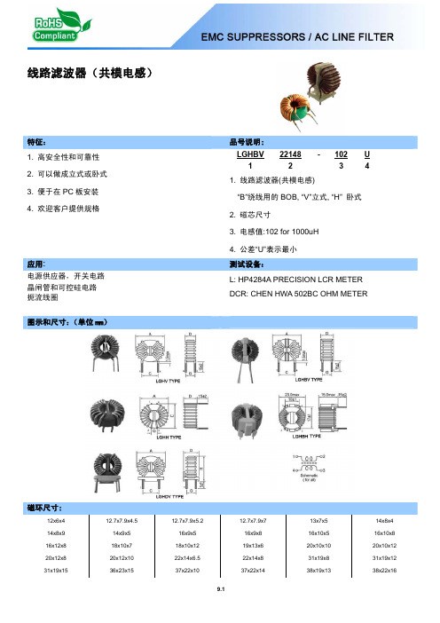
1. 线路滤波器(共模电感) “B”绕线用的 BOB, “V”立式, “H” 卧式 2. 磁芯尺寸 3. 电感值:102 for 1000uH 4. 公差“U”表示最小
应用: 电源供应器,开关电路 晶闸管和可控硅电路 扼流线圈 图示和尺寸: (单位 mm)
测试设备: L: HP4284A PRECISION LCR METER DCR: CHEN HWA 502BC OHM METER
9.2
便于在pc板安装欢迎客户提供规格lghbv22148线路滤波器共模电感b绕线用的bobv立式公差u表示最小应用
线路滤波器(共模电感)
特征: 1. 高安全性和可靠性 2. 可以做成立式或卧式 3. 便于在 PC 板安装 4. 欢迎客户提供规格
品号说明: LGHBV 1 22148 2 102 14x8x9 16x12x8 20x12x8 31x19x15 12.7x7.9x4.5 14x9x5 18x10x7 20x12x10 36x23x15 12.7x7.9x5.2 16x9x5 18x10x12 22x14x6.5 37x22x10 9.1 12.7x7.9x7 16x9x8 19x13x6 22x14x8 37x22x14 13x7x5 16x10x5 20x10x10 31x19x8 38x19x13 14x8x4 16x10x8 20x10x12 31x19x12 38x22x16
图示和尺寸: (单位 mm)
电气特性参数
电感量 品号 (mH)Min 103U-0.1A 802U-0.2A LU9.8 LUH9.8 502U-0.2A 502U-0.3A 202U-0.5A 501U-1A LU10-103U-0.3A LU10-502U-0.5A LU10-402U-0.7A LU10-302U-1A LU10-202U-1A LU10-102U-1.5A LU10-601U-2A LU16-303U-0.4A LU16-203U-0.5A LU16-103U-0.6A LU16-802U-0.8A LU16-602U-1A LU16-252U-1.2A LU16-152-1.5A LUT20-333U-0.3A LUT20-223U-0.4A LUT20-153U-0.5A LUT20-103U-0.7A LUT20-682U-0.8A LUT20-472U-1A LUT20-332U-1A LUT20-222U-1.2A LUT20-152U-1.5A LUT20-751U-1.8A 10.0 8.0 5.0 5.0 2.0 0.5 10.0 5.0 4.0 3.0 2.0 1.0 0.6 30 20 10 8.0 6.0 2.5 1.5 33 22 15 10 6.8 4.7 3.3 2.2 1.5 0.75 (Ω) Max 8.0 6.0 4.5 3.5 1.0 0.3 3.0 1.5 1.0 0.5 0.5 0.2 0.2 2.8 1.6 1.2 0.8 0.5 0.25 0.15 2.5 1.7 1.2 0.75 0.53 0.38 0.31 0.18 0.14 0.12 直流电阻
31012709_Liebert NX 30kVA和40kVA UPS_V1.0_3.4用户手册

1.若长时间存储或放置不使用,必须将本产品置于干燥、洁净和规定温度范围的环境中。 2.本产品应在适当的工作环境中使用(详见本产品手册环境要求章节)。 3.禁止在以下工作环境中使用本产品:
超出本产品技术指标规定的高温、低温或潮湿场所 有导电粉尘、腐蚀性气体、盐雾或可燃性气体的场所 有振动、易受撞的场所 靠近热源或有强电磁场干扰的场所
1.1 特点.........................................................................................................................................................................................1 1.2 设计思想.................................................................................................................................................................................1
一般安全
与其它类型的大功率设备一样,UPS 及电池开关盒/电池柜内部带有高压。但由于带高压的元器件只有打开前门(有锁)才可 能接触到,所以接触高压的可能性已降到最小。本设备符合 IP20 标准,内部还有其它的安全屏蔽。 如果遵照一般规范并按照本书所建议的步骤进行设备的操作,将不会存在任何危险。
用户可维护器件
目录
第一章 概述 ........................................................................................................................................................................ 1
NEC Tokin Product Guide
10K 1K 100 10
Impedance (⏲)
02-200
10K 1K 100 10
02-100
02-300
02-500
02-101
3 6 1 3 6 1 3 6 1 3 6 1 3
1 1K
10K
100K
1M
10M
30M
1 1K
3
6
1
3
6
1
3
6
1
3
6
1
3
10K
100K
1M
10M
30M
Frequency (Hz)
●本PDF商品目录的内容发生变更或停止生产時,恕不另行通知,请在订购时确认最新信息。 ●在订购本PDF商品目录中的产品时,请申请交货规格书,以便进一步确认更详细的规格参数。 ●在使用本PDF商品目录中的产品时,请确认印刷版商品目录中的“安全相关注意事项”的内容以及其他与安全有关的注意事项。
0001EMCVOL01C1503E1
0001EMCVOL01C1503E1
公模
SC Coils 标准型
[RoHS [RoHS 对应品 对应品] ]
型号
最大定额电流 (A)
SC-02-101 SC-02-100 SC-02-200 SC-02-300 SC-02-500 SC-02-800 SC-05-100 SC-05-200 SC-05-500 SC-05-800 SC-10-100 SC-10-200 SC-15-100 SC-15-200 SC-20-100 SC-30-100
2 2 2 2 5 5 5 4 4 10 10 10 12 15 15 18
电感值 (mH) 最小 1 2 3 5 1 2 3 5 8 1 2 3 1.5 0.5 1 0.5
10uh大电流贴片电感选型
声明:1、本规格书若有变更,恕不另行通知,请在订购时确认;2、本规格书没有足够的空间说明详细电性能参数,仅列明了标准规格,在订购产品之前谨请与客服或选型工程师确认。
L(长)尺寸 1.6±0.2mm W(宽)尺寸0.8±0.2mm T(高)尺寸0.8±0.2mm D(电极宽度)尺寸0.3±0.2mm 英制封装代号0603公制封装代号160808声明:1、本规格书若有变更,恕不另行通知,请在订购时确认;2、本规格书没有足够的空间说明详细电性能参数,仅列明了标准规格,在订购产品之前谨请与客服或选型工程师确认。
L(长)尺寸 1.6±0.2mm W(宽)尺寸0.8±0.2mm T(高)尺寸0.8±0.2mm D(电极宽度)尺寸0.3±0.2mm 英制封装代号0603公制封装代号160808声明:1、本规格书若有变更,恕不另行通知,请在订购时确认;2、本规格书没有足够的空间说明详细电性能参数,仅列明了标准规格,在订购产品之前谨请与客服或选型工程师确认。
L(长)尺寸 1.6±0.2mm W(宽)尺寸0.8±0.2mm T(高)尺寸0.8±0.2mm D(电极宽度)尺寸0.3±0.2mm 英制封装代号0603公制封装代号160808CMP201209XD100K/M/N 贴片电感选型表声明:1、本规格书若有变更,恕不另行通知,请在订购时确认;2、本规格书没有足够的空间说明详细电性能参数,仅列明了标准规格,在订购产品之前谨请与客服或选型工程师确认。
声明:1、本规格书若有变更,恕不另行通知,请在订购时确认;2、本规格书没有足够的空间说明详细电性能参数,仅列明了标准规格,在订购产品之前谨请与客服或选型工程师确认。
L(长)尺寸 2.0±0.2mm W(宽)尺寸 1.2±0.2mm T(高)尺寸0.9±0.2mm D(电极宽度)尺寸0.5±0.3mm 英制封装代号0805公制封装代号201209声明:1、本规格书若有变更,恕不另行通知,请在订购时确认;2、本规格书没有足够的空间说明详细电性能参数,仅列明了标准规格,在订购产品之前谨请与客服或选型工程师确认。
共模电感 uh
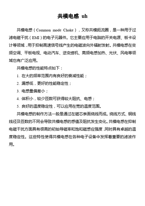
共模电感uh
共模电感(Common mode Choke),又称共模扼流圈,是一种用于过滤电磁干扰(EMI)的电子元器件。
它主要应用于电脑的开关电源、板卡设计等领域,用于抑制高速信号线产生的电磁波向外辐射发射。
共模电感在变频空调、平板电视、电动汽车、逆变焊机、高频电感加热、光伏、风电等领域也有广泛应用。
共模电感的性能特点如下:
1. 在大的频率范围内有良好的衰减性能;
2. 漏感低,更好的性能稳定性;
3. 电感量偏差小;
4. 体积小,较少匝数可获得较大阻抗、电感;
5. 良好的温度稳定性,可以应用在宽的温度范围。
共模电感的制作方法一般是通过在磁芯表面绕线而成。
绕线方式、铜线线径及匝数的不同会导致共模电感的感值及阻抗发生变化。
共模电感在抑制电磁干扰方面具有很高的初始导磁率和饱和磁感应强度,同时具有卓越的温度稳定性。
这些特性使得共模电感在各种电子设备中发挥着重要的滤波作用。
淼田电子有限公司LQG15HH系列芯片电感说明书
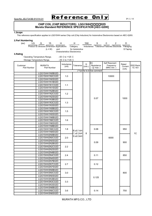
SpecNo.JELF243B-9101H-01 P.1 / 11Reference OnlyCHIP COIL (CHIP INDUCTORS) LQG15HH □□□□02DMurata Standard REFERENCE SPECIFICATION [AEC-Q200]1.ScopeThis reference specification applies to LQG15HH series Chip coil (Chip Inductors) for Automotive Electoronics based on AEC-Q200.2.Part Numbering(ex) LQ G 15 H H 1N0 S 0 2 DProduct ID Struture Dimension Applications Category Inductance Tolerance Features Electrode Pakaging(L ×W) and for Automotive D:TapingCharacteristics Electoronics3.Rating・Operating Temperature Range. –55°C to +125°C ・Storage Temperature Range. –55°C to +125°CCustomer Part Number MURATAPart NumberInductance (nH) ToleranceQ(min.)DC Resistance (Ω max. ) Self ResonantFrequency (MHz min. )Rated Current (mA)ESD Rank 1C:1kV(*1)(refer to below comment)LQG15HH1N0B02D1.0B:±0.1nHC:±0.2nH S:±0.3nH8 0.07 10000 10001CLQG15HH1N0C02D LQG15HH1N0S02D LQG15HH1N1B02D1.1 6000 LQG15HH1N1C02DLQG15HH1N1S02D LQG15HH1N2B02D 1.2 LQG15HH1N2C02D LQG15HH1N2S02DLQG15HH1N3B02D1.3 LQG15HH1N3C02DLQG15HH1N3S02D LQG15HH1N5B02D1.5 LQG15HH1N5C02DLQG15HH1N5S02D LQG15HH1N6B02D 1.6 LQG15HH1N6C02D LQG15HH1N6S02D LQG15HH1N8B02D 1.8 0.08 950LQG15HH1N8C02D LQG15HH1N8S02DLQG15HH2N0B02D2.0 0.09 900LQG15HH2N0C02DLQG15HH2N0S02DLQG15HH2N2B02D 2.2 LQG15HH2N2C02D LQG15HH2N2S02D LQG15HH2N4B02D2.4 0.11 850 LQG15HH2N4C02DLQG15HH2N4S02D LQG15HH2N7B02D 2.7 0.12 800 LQG15HH2N7C02D LQG15HH2N7S02D LQG15HH3N0B02D 3.0 0.125LQG15HH3N0C02D LQG15HH3N0S02DLQG15HH3N3B02D3.3 LQG15HH3N3C02DLQG15HH3N3S02D LQG15HH3N6B02D3.6 0.14 750 LQG15HH3N6C02DLQG15HH3N6S02DCustomer Part Number MURATAPart NumberInductance (nH) ToleranceQ(min.)DC Resistance (Ω max. ) Self ResonantFrequency(MHz min. )RatedCurrent(mA)ESD Rank 1C:1kV(*1)(refer to below comment)LQG15HH3N9B02D3.9 B:±0.1nHC:±0.2nHS:±0.3nH8 0.14 6000 7501CLQG15HH3N9C02DLQG15HH3N9S02DLQG15HH4N3B02D 4.3 LQG15HH4N3C02D LQG15HH4N3S02D LQG15HH4N7B02D 4.7 0.16 700LQG15HH4N7C02D LQG15HH4N7S02DLQG15HH5N1B02D5.1 0.18 5300 650LQG15HH5N1C02DLQG15HH5N1S02DLQG15HH5N6B02D5.6 4500 LQG15HH5N6C02DLQG15HH5N6S02D LQG15HH6N2B02D6.2 0.20 600LQG15HH6N2C02DLQG15HH6N2S02DLQG15HH6N8G02D6.8 G:±2%H:±3%J:±5%0.22 LQG15HH6N8H02DLQG15HH6N8J02D LQG15HH7N5G02D 7.5 0.24 4200 550LQG15HH7N5H02D LQG15HH7N5J02DLQG15HH8N2G02D 8.2 3700 LQG15HH8N2H02D LQG15HH8N2J02DLQG15HH9N1G02D 9.1 0.26 3400500LQG15HH9N1H02D LQG15HH9N1J02DLQG15HH10NG02D10 LQG15HH10NH02D LQG15HH10NJ02D LQG15HH12NG02D12 0.28 3000 LQG15HH12NH02DLQG15HH12NJ02DLQG15HH15NG02D15 0.32 2500 450 LQG15HH15NH02DLQG15HH15NJ02D LQG15HH18NG02D18 0.36 2200 400 LQG15HH18NH02DLQG15HH18NJ02D LQG15HH22NG02D 22 0.42 1900 350 LQG15HH22NH02D LQG15HH22NJ02D LQG15HH27NG02D 27 0.46 1700 LQG15HH27NH02D LQG15HH27NJ02D LQG15HH33NG02D33 0.58 1600 LQG15HH33NH02DLQG15HH33NJ02D LQG15HH39NG02D39 0.65 1200 300 LQG15HH39NH02DLQG15HH39NJ02DCustomer Part Number MURATAPart NumberInductance (nH) Tolerance Q(min.) DC Resistance (Ω max. ) Self Resonant Frequency (MHz min. )Rated Current (mA)ESD Rank 1C:1kV(*1)(refer to below comment)LQG15HH47NG02D 47 G:±2%H:±3%J:±5%8 0.72 1000 3001CLQG15HH47NH02D LQG15HH47NJ02DLQG15HH56NG02D 56 0.82 800 250LQG15HH56NH02D LQG15HH56NJ02DLQG15HH68NG02D68 0.92 LQG15HH68NH02DLQG15HH68NJ02D LQG15HH82NG02D82 1.20 700 200 LQG15HH82NH02DLQG15HH82NJ02D LQG15HHR10G02D100 1.25 600 LQG15HHR10H02DLQG15HHR10J02DLQG15HHR12G02D120 1.30 LQG15HHR12H02DLQG15HHR12J02DLQG15HHR15G02D 150 2.99 550 150LQG15HHR15H02D LQG15HHR15J02DLQG15HHR18G02D 180 3.38 500 LQG15HHR18H02D LQG15HHR18J02D LQG15HHR22G02D 220 3.77 450 120 LQG15HHR22H02D LQG15HHR22J02D LQG15HHR27G02D270 4.94 400 110 LQG15HHR27H02DLQG15HHR27J02D(*1) Standard Testing Conditions《Unless otherwise specified 》 《In case of doubt 》Temperature : Ordinary Temperature / 15°C to 35°C Temperature: 20°C ± 2°CHumidity :Ordinary Humidity / 25%(RH) to 85%(RH) Humidity : 60%(RH) to 70%(RH) Atmospheric Pressure : 86kPa to 106 kPa4. Appearance and Dimensions■Unit Mass (Typical value)6.Q200 Requirement6.1.Performance (based on Table 5 for Magnetics(Inductors / Transformer)AEC-Q200 Rev.D issued June 1. 2010AEC-Q200 Murata Specification / Deviation No Stress TestMethod3 HighTemperatureExposure 1000hours at 125 deg CSet for 24hours at roomtemperature, then measured.Meet Table A after testing.Table A4 TemperatureCycling 1000cycles-40 deg C to +125 deg CSet for 24hours at roomtemperature,thenmeasured.Meet Table A after testing.7 Biased Humidity 1000hours at 85 deg C, 85%RHunpowered.Meet Table A after testing.8 Operational Life Apply 125 deg C 1000hoursSet for 24hours at roomtemperature, then measuredMeet Table A after testing.9 External Visual Visual inspection No abnormalities10 Physical Dimension Meet ITEM 4(Style and Dimensions)No defects12 Resistanceto Solvents PerMIL-STD-202Method 215Not ApplicableAppearance No damageInductanceChange(at 100MHz)Within ±10%AEC-Q200 Murata Specification / Deviation No Stress TestMethod13 Mechanical Shock Per MIL-STD-202Method 213Condition C : 100g’s(0.98N),6ms, Half sine, 12.3ft/sMeet Table A after testing.14 Vibration 5g's(0.049N) for 20 minutes,12cycles each of 3 oritentationsTest from 10-2000Hz.Meet Table A after testing.15 Resistanceto Soldering Heat No-heatingSolder temperature260C+/-5 deg CImmersion time 10sMeet Table A after testing.Pre-heating 150C +/-10 deg C, 60s to 90s17 ESD Per AEC-Q200-002 ESD Rank: refer to the Item3 (Rating).Meet Table A after testing18 Solderbility Per J-STD-002 Method b : Not Applicable90% of the terminations is to be soldered.19 ElectricalCharacterizationMeasured : Inductance No defects20 Flammability Per UL-94 Not Applicable21 Board Flex Epoxy-PCB(1.6mm)Deflection 2mm(min)Holding time 60s Meet Table B after testing.Table BAppearance No damage DCresistanceChangeWithin ±10%22 Terminal Strength Per AEC-Q200-006A force of 17.7Nfor 60s Murata Deviation Request: 5N No defects7.Specification of Packaging(in mm)7.2 Specification of Taping(1) Packing quantity (standard quantity)10,000 pcs. / reel(2) Packing MethodProducts shall be packed in the cavity of the base tape and sealed by top tape and bottom tape.(3) Sprocket holeThe sprocket holes are to the right as the tape is pulled toward the user.(4) Spliced pointBase tape and Top tape has no spliced point.(5) Missing components numberMissing components number within 0.1 % of the number per reel or 1 pc., whichever is greater,andare not continuous. The Specified quantity per reel is kept.0.8m ax.7.3 Pull StrengthTop tape5N min.Bottom tape7.4 Peeling off force of cover tapeSpeed of Peeling off 300mm/min Peeling off force0.1N to 0.6N(minimum value is typical)7.5 Dimensions of Leader-tape,Trailer and ReelThere shall be leader-tape ( top tape and empty tape) and trailer-tape (empty tape) as follows.7.6 Marking for reelCustomer part number, MURATA part number, Inspection number(*1) ,RoHS Marking(*2), Quantity etc ・・・*1) <Expression of Inspection No.> □□ OOOO ⨯⨯⨯(1) (2) (3)(1) Factory Code (2) Date First digit : Year / Last digit of yearSecond digit: Month / Jan. to Sep. → 1 to 9, Oct. to Dec. → O, N, D Third, Fourth digi : Day(3) Serial No.*2) <Expression of RoHS Marking> ROHS – Y (△)(1) (2)(1) RoHS regulation conformity parts. (2) MURATA classification number7.7 Marking for Outside package (corrugated paper box)Customer name, Purchasing order number, Customer part number, MURATA part number, RoHS Marking(*2) ,Quantity, etc ・・・7.8. Specification of Outer CaseOuter Case Dimensions(mm)Standard Reel Quantityin Outer Case (Reel)W D H 186 186 93 5* Above Outer Case size is typical. It depends on a quantity of an order.F165to 180degreeTop tape Bottom tapeBase tapeWDLabelH8. △!Caution8.1 Caution(Rating)Do not exceed maximum rated current of the product. Thermal stress may be transmitted to the product and short/open circuit of the product or falling off the product may be occurred.8.2 Fail-safe Be sure to provide an appropriate fail-safe function on your product to prevent a second damage that may becaused by the abnormal function or the failure of our product.8.3 Limitation of ApplicationsPlease contact us before using our products for the applications listed below which require especially high reliability for the prevention of defects which might directly cause damage to the third party's life, body or property.(1) Aircraft equipment (6) Transportation equipment (trains, ships, etc.) (2) Aerospace equipment (7) Traffic signal equipment(3) Undersea equipment (8) Disaster prevention / crime prevention equipment (4) Power plant control equipment (9) Data-processing equipment (5) Medical equipment (10) Applications of similar complexity and /or reliability requirements to the applications listed in the above9. NoticeProducts can only be soldered with reflow. This product is designed for solder mounting.Please consult us in advance for applying other mounting method such as conductive adhesive.9.1 Land pattern designinga 0.4b 1.4 to 1.5c 0.5 to 0.6(in mm)9.2 Flux, Solder・Use rosin-based flux.Don’t use highly acidic flux with halide content exceeding 0.2(wt)% (chlorine conversion value). Don’t use water-soluble flux. ・Use Sn-3.0Ag-0.5Cu solder.・Standard thickness of solder paste : 100μm to 150μm.Resist9.3 Reflow soldering conditions・Inductance value may be changed a little due to the amount of solder.So, the chip coil shall be soldered by reflow so that the solder volume can be controlled.・Pre-heating should be in such a way that the temperature difference between solder and product surface is limited to 150°C max. Cooling into solvent after soldering also should be in such a way that the temperature difference is limited to 100°C max.Insufficient pre-heating may cause cracks on the product, resulting in the deterioration of products quality. ・Standard soldering profile and the limit soldering profile is as follows.The excessive limit soldering conditions may cause leaching of the electrode and / or resulting in the deterioration of product quality.・Reflow soldering profileStandard Profile Limit Profile Pre-heating 150°C ~180°C 、90s ±30s Heating above 220°C 、30s ~60s above 230°C 、60s max. Peak temperature 245°C ±3°C 260°C,10s Cycle of reflow 2 times 2 times9.4 Reworking with soldering ironThe following conditions must be strictly followed when using a soldering iron.Pre-heating 150°C,1 min Tip temperature 350°C max. Soldering iron output 80W max. Tip diameter φ3mm max. Soldering time 3(+1,-0)sTime 2 timesNote :Do not directly touch the products with the tip of the soldering iron in order to prevent the crack on the products due to the thermal shock.9.5 Solder Volume・ Solder shall be used not to be exceed the upper limits as shown below.・ Accordingly increasing the solder volume, the mechanical stress to Chip is also increased. Exceeding solder volume may cause the failure of mechanical or electrical performance.1/3T ≦t ≦TT :thickness of product9.6 Mount ShockOver Mechanical stress to products at mounting process causes crack and electrical failure etc.Limit ProfileStandard Profile 90s±30s 230℃260℃245℃±3℃220℃30s~60s 60s max.180150Temp.(s)(℃)Time.9.7 Product’s locationThe following shall be considered when designing and laying out P.C.B.'s.(1) P.C.B. shall be designed so that products are not subjected to the mechanical stress due to warping the board.[Products direction ]Products shall be located in the sideways direction (Length:a <b) to the mechanical stress.(2) Components location on P.C.B. separation. It is effective to implement the following measures, to reduce stress in separating the board.It is best to implement all of the following three measures; however, implement as many measures as possible to reduce stress.Contents of MeasuresStress Level (1) Turn the mounting direction of the component parallel to the board separation surface. A > D *1 (2) Add slits in the board separation part.A >B (3) Keep the mounting position of the component away from the board separation surface. A > C*1 A > D is valid when stress is added vertically to the perforation as with Hand Separation.If a Cutting Disc is used, stress will be diagonal to the PCB, therefore A > D is invalid.(3) Mounting Components Near Screw HolesWhen a component is mounted near a screw hole, it may be affected by the board deflection that occurs during the tightening of the screw. Mount the component in a position as far away from the screw holes as possible.9.8 Cleaning ConditionsProducts shall be cleaned on the following conditions.(1) Cleaning temperature shall be limited to 60°C max.(40°C max for IPA.)(2) Ultrasonic cleaning shall comply with the following conditions with avoiding the resonance phenomenon at the mounted products and P.C.B.Power : 20 W / l max. Frequency : 28kHz to 40kHz Time : 5 min max.(3) Cleaner1. Alcohol type cleanerIsopropyl alcohol (IPA)2. Aqueous agentPINE ALPHA ST-100S(4) There shall be no residual flux and residual cleaner after cleaning. In the case of using aqueous agent, products shall be dried completely after rinse with de-ionized water in order to remove the cleaner. (5) Other cleaning Please contact us.〈Poor example 〉〈Good example 〉ba9.9 Resin coatingThe inductance value may change and/or it may affect on the product's performance due to highcure-stress of resin to be used for coating / molding products. So please pay your careful attention whenyou select resin.In prior to use, please make the reliability evaluation with the product mounted in your application set.9.10 Handling of a substrateAfter mounting products on a substrate, do not apply any stress to the product caused by bending ortwisting to the substrate when cropping the substrate, inserting and removing a connector from thesubstrate or tightening screw to the substrate.Excessive mechanical stress may cause cracking in the product.Bending Twisting9.11 Storage and Handing Requirements(1) Storage periodUse the products within 6 months after deliverd.Solderability should be checked if this period is exceeded.(2) Storage conditions・Products should be stored in the warehouse on the following conditions.Temperature: -10°C to 40°CHumidity: 15% to 85% relative humidity No rapid change on temperature and humidityDon't keep products in corrosive gases such as sulfur,chlorine gas or acid, or it may causeoxidization of electrode, resulting in poor solderability.・Products should be storaged on the palette for the prevention of the influence from humidity, dust and so on.・Products should be storaged in the warehouse without heat shock, vibration, direct sunlight and so on.・Products should be storaged under the airtight packaged condition.(3) Handling ConditionCare should be taken when transporting or handling product to avoid excessive vibration or mechanical shock.10.△!Note(1) Please make sure that your product has been evaluated in view of your specifications with our product being mounted to your product.(2) You are requested not to use our product deviating from the reference specifications.(3) The contents of this reference specification are subject to change without advance notice.Please approve our product specifications or transact the approval sheet for product specificationsbefore ordering.Reference OnlySpecNo.JELF243B-9101H-01 P.11 / 11。
共模电感2.5mh 10a

共模电感2.5mh 10a
摘要:
1.共模电感的介绍
2.共模电感的参数
3.共模电感的应用领域
正文:
共模电感是一种电子元件,其主要作用是在电路中抑制共模干扰。
共模电感的参数通常包括电感值、电流和电压等。
其中,电感值是衡量共模电感性能的重要指标,通常以毫亨(mH)为单位。
电流则表示共模电感所能承受的最大电流值,而电压则表示共模电感所能承受的最大电压值。
在这篇文章中,我们将主要介绍共模电感的一些基本参数,包括电感值、电流等,并探讨共模电感在实际应用中的重要作用。
共模电感的电感值通常在几毫亨到几十毫亨之间,这取决于共模电感的具体类型和应用场景。
电感值越小,共模电感的抑制能力就越强,但同时其体积也会更小。
电感值越大,共模电感的抑制能力就越弱,但同时其体积也会更大。
共模电感的电流参数通常在几安培到几十安培之间,这取决于共模电感的具体类型和应用场景。
电流越大,共模电感的抑制能力就越强,但同时其体积也会更大。
电流越小,共模电感的抑制能力就越弱,但同时其体积也会更小。
共模电感广泛应用于电子设备中,主要用于抑制电源线上的共模干扰。
共模干扰是指电源线上的噪声信号,这些信号可能来自其他电子设备或外部电磁
场。
共模电感能够有效地抑制这些干扰信号,从而保证电子设备的正常工作。
总之,共模电感是一种非常重要的电子元件,其参数包括电感值和电流等。
常用共模电感外型图
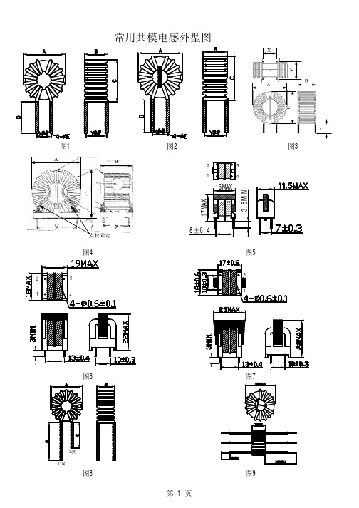
*CMI350uH/1A/H9 1.0350321768VDC 12645图1、2*CMI500uH/1A/H10 1.0500391768VDC 13 6.545图1、2*CMI2.0mH/1A/H14 1.020********VDC 17968图1、2CMI1.5mH/1A/H14 1.01500791768VDC 17968图1、2CMI1.0mH/1A/H14 1.010********VDC 17968图1、2CMI2.0mH/1.5A/H14 1.52000501768VDC 17968图1、2CMI1.5mH/1.5A/H14 1.51500441768VDC 17968图1、2CMI1.0mH/1.5A/H14 1.51000371768VDC 17968图1、2*CMI1.5mH/2A/H14 2.01500441768VDC 17968图1、2CMI1.0mH/2A/H14 2.010********VDC 17968图1、2CMI500uH/3A/H14 3.0500151768VDC 18968图1、2CMI350uH/3A/H14 3.0350131768VDC 18968图1、2CMI240uH/3A/H14 3.024*******VDC 18968图1、2CMI170uH/4A/H14 4.017071768VDC 18968图1、2CMI170uH/5A/H14 5.017061768VDC 19968图1、2CMI6.0mH/1A/H1608 1.060001571768VDC 1912711图1、2CMI4.2mH/1A/H1608 1.042001301768VDC 1912711图1、2CMI3.0mH/1A/H1608 1.030001131768VDC 1912711图1、2CMI4.2mH/1.5A/H1608 1.54200731768VDC 2013711图1、2CMI3.0mH/1.5A/H1608 1.53000641768VDC 2013711图1、2CMI3.0mH/2A/H160808 2.03000541768VDC 1912711图1、2CMI2.0mH/2A/H1608 2.020********VDC 1912711图1、2*CMI1.5mH/3A/H1608 3.01500251768VDC 2013712图1、2CMI1.0mH/3A/H1608 3.010********VDC 2013712图1、2CMI700uH/3A/H1608 3.0700191768VDC 2013712图1、2CMI500uH/4A/H1608 4.0500121768VDC 2013712图1、2CMI350uH/4A/H1608 4.0350101768VDC 2013712图1、2CMI350uH/5A/H1608 5.035091768VDC 2013712图1、2CMI240uH/6A/H1608 6.025061768VDC 2014712图1、2CMI170uH/7A/H16087.017051768VDC 2014712图1、2CMI3.0mH/1A/H1605 1.030001161768VDC 198.578图1、2CMI2.0mH/1A/H1605 1.020********VDC 198.578图1、2CMI3.0mH/1.5A/H1605 1.53000651768VDC 198.578图1、2CMI1.5mH/2A/H1605 2.01500391768VDC 198.578图1、2CMI1.0mH/2A/H1605 2.010********VDC 198.578图1、2CMI700uH/2A/H1605 2.0700281768VDC 198.578图1、2CMI1.0mH/3A/H1605 3.010********VDC 20978图1、2CMI700uH/3A/H1605 3.0700181768VDC 20978图1、2CMI350uH/4A/H1605 4.0350111768VDC 20978图1、2CMI240uH/5A/H1605 5.025071768VDC 201078图1、2CMI3.0mH/2A/H18 2.03000611768VDC 21978.5图1、2CMI2.0mH/2A/H18 2.020********VDC 21978.5图1、2CMI1.5mH/2A/H18 2.01500431768VDC 21978.5图1、2*CMI2.0mH/3A/H18 3.020********VDC 221078.5图1、2CMI1.5mH/3A/H18 3.01500291768VDC 221078.5图1、2*CMI700uH/4A/H18 4.0700151768VDC 2210.578.5图1、2CMI500uH/4A/H184.0500131768VDC221078.5图1、2MAX MAX 参考参考MAX 1mA,5s @1kHz,0.3V 流(A)流(A)MAX MAX参考参考@1kHz,0.3VMAX1mA,5sCMI500uH/5A/H18 5.0500111768VDC231178.5图1、2 CMI350uH/5A/H18 5.035091768VDC231178.5图1、2 CMI350uH/6A/H18 6.035071768VDC231178.5图1、2 CMI7.0mH/2A/H22H 2.07000992000VAC2916912图3 CMI6.0mH/2A/H22H 2.06000912000VAC2916912图3 CMI4.2mH/2A/H22H 2.04200782000VAC2815912图3 CMI6.0mH/3A/H22H 3.06000602000VAC2916912图3 *CMI4.2mH/3A/H22H 3.04200502000VAC2814912图3 CMI3.0mH/3A/H22H 3.03000432000VAC2814912图3 CMI1.5mH/4A/H22H 4.01500242000VAC2914912图3 CMI1.0mH/4A/H22H 4.010********VAC2914912图3 *CMI1.0mH/5A/H22H 5.010********VAC2813912图3 CMI700uH/5A/H22H 5.0700142000VAC2914912图3 CMI700uH/6A/H22H 6.0700112000VAC3014912图3 CMI500uH/7A/H22H7.050082000VAC3014912图3 CMI1.0mH/8A/H22H8.010********VAC3014912图3 CMI700uH/8A/H22H8.070062000VAC3014912图3 CMI20mH/3AY/H25 3.0200001212000VAC322217.515图4 CMI15mH/3AY/H25 3.0150001052000VAC322217.515图4 CMI10mH/3AY/H25 3.010*********VAC322217.515图4 CMI7.0mH/3AY/H25 3.07000722000VAC322217.515图4 CMI10mH/4AY/H25 4.010*********VAC322217.515图4 CMI7.0mH/4AY/H25 4.07000572000VAC322217.515图4 CMI6.0mH/4AY/H25 4.06000522000VAC322217.515图4 CMI4.2mH/4AY/H25 4.04200442000VAC322217.515图4 CMI3.0mH/4AY/H25 4.03000382000VAC322217.515图4 CMI2.0mH/4AY/H25 4.020********VAC322217.515图4 *CMI3.0mH/5AY/H25 5.03000312000VAC322217.515图4 CMI2.0mH/5AY/H25 5.020********VAC332217.515图4 CMI1.5mH/5AY/H25 5.01500222000VAC332217.515图4 CMI2.0mH/6AY/H25 6.020********VAC332217.515图4 CMI1.5mH/6AY/H25 6.01500182000VAC332217.515图4 CMI1.0mH/6AY/H25 6.010********VAC332217.515图4 CMI2.0mH/7AY/H257.020********VAC342317.515图4 CMI1.5mH/7AY/H257.01500162000VAC342317.515图4 CMI1.0mH/7AY/H257.010********VAC342317.515图4 CMI1.5mH/8AY/H258.01500132000VAC342317.515图4 *CMI1.0mH/10AY/H2510.010*******VAC342317.515图4 CMI700uH/10AY/H2510.070072000VAC342317.515图4 *CMI30uH/1A/H8* 1.02027500VDC10433图8 *CMI16mH/1A/W14** 1.0160001742000VAC181068图1、2 *3CMI2.0mH/8A/H318.020********VAC3820---CMI15mH/0.2A/U9.80.21500023302000VAC----图5 CMI10mH/0.2A/U9.80.21000018922000VAC----图5 CMI6.0mH/0.3A/U9.80.360009032000VAC----图5 CMI4.2mH/0.3A/U9.80.342007572000VAC----图5 CMI3.0mH/0.3A/U9.80.330006472000VAC----图5流(A)MAX1mA,5sMAX MAX参考参考@1kHz,0.3VCMI2.0mH/0.3A/U9.80.320005252000VAC----图5 CMI1.5mH/0.3A/U9.80.315004642000VAC----图5 CMI1.0mH/0.3A/U9.80.310003792000VAC----图5 *CMI2.0mH/0.5A/U9.80.520003092000VAC----图5 CMI1.5mH/0.5A/U9.80.515002732000VAC----图5 CMI1.0mH/0.5A/U9.80.510002232000VAC----图5 *CMI500uH/1A/U9.8 1.0500702000VAC----图5 CMI35mH/0.3A/U100.33500021042000VAC----图6 CMI28mH/0.3A/U100.32800018862000VAC----图6 CMI20mH/0.3A/U100.32000015892000VAC----图6 CMI15mH/0.3A/U100.31400013402000VAC----图6 CMI10mH/0.3A/U100.31000011212000VAC----图6 *CMI15mH/0.5A/U100.5140007872000VAC----图6 CMI10mH/0.5A/U100.5100006592000VAC----图6 CMI7.0mH/0.5A/U100.570005582000VAC----图6 *CMI3.0mH/1A/U10 1.030001622000VAC----图6 CMI2.0mH/1A/U10 1.020*********VAC----图6 CMI1.5mH/1A/U10 1.015001182000VAC----图6 CMI1.0mH/2A/U10 2.010********VAC----图6 *CMI4.2mH/2A/U16 2.04200922000VAC----图7 CMI3.0mH/2A/U16 2.03000782000VAC----图7 CMI2.0mH/2A/U16 2.020********VAC----图7 CMI1.5mH/2A/U16 2.01500552000VAC----图7 CMI1.0mH/2A/U16 2.010********VAC----图7 *CMI1.5mH/3A/U16 3.01500312000VAC----图7 CMI1.0mH/3A/U16 3.010********VAC----图7 CMI1.0mH/4A/U16 4.010********VAC----图7说明:此系列器件电流密度取值为6A/mm2,型号后面带*的为镍锌磁芯绕制,带**的为非晶磁芯绕制。