MPX2700A中文资料
Z23S4407N中文资料(AEROVOX)中文数据手册「EasyDatasheet - 矽搜」
• 专利压力灭弧符合UL810
每个电容器填充有环氧化Soybeanoil
要求.
电介液.大豆油已被证明可靠性
•环防护专利非PCB
在几个过去几十年.大豆油是
环氧大豆油.
环防护和可生物降解.该
大豆油防护护金属化膜不受腐蚀,
认证证书
助剂传热,并有助于抑制降解
电晕效应,这可能导致否则prema-
UL和CUL文件编号E51176
所有AEROMET II电容都可以用时间和成本节约
EIA RS-186-3E状态测试要求.
AeroMount系统.触点厂家触点厂家对于需要reycled了解详细信息.
认证证书
EIA RS-186-2E湿度测试要求(TropiCAL条件).
• UL文件号E51176
• CSA文件号058450
• VDE认证可用
电压编码 电压第一个两位数
24 = 240 V交流 33 = 330 V交流 37 = 370 V交流 44 = 440 V交流 48 = 480 V交流 60 = 600 Vac
电容值
(μF额定值) 25 = 25 µF 03 = 3 µF)
工厂代码
AeroMet II 00 =单额定值 XX =μF价值
产品系列
M = AeroMet II Z = SuperMet & ZeMax TM
机箱样式
22 = 1½"圆 23 = 1.75"圆 24 = 2.0"圆 26 = 2½"圆
50 = 1.25"椭圆形 42 = 1½"椭圆形 64 = 1.75"椭圆形 62 = 2.0"椭圆形
注入
P = Supernol(M系列) S = SuperSoy(Z系列)
HART Multiplexer Master HiDMux2700说明书

HART Multiplexer MasterHiDMux2700<32-channel<24 V DC supply<HART field device input (revision 5 to 7)<RS-485 interface<Up to SIL 3 acc. to IEC 61508HART Multiplexer MasterThe HART Multiplexer Master provides 32 signal channels for connection to SMART transmitters or control devices supporting digital communication according to the HART standard.Full three-port isolation is included and each input channel has dual capacitor isolation for freedom of loop connection.Each HART Multiplexer Master is networked simply by connecting the high-speed RS 485 output in a multidrop configuration.The device interrogates each field device, under the supervision of the workstation, retrieving information for storage in its internal database, which is then easily accessed.This module is intended to mount on an HiD Termination Board or HART Communcation Board. Also special boards for DCS integration are available.For additional information, refer to the manual and .RS 485Zone 2Div. 224 V DCedate:221-1-22Dateofissue:221-1-22Filename:211968_eng.pdfe d a t e : 2021-01-22 D a t e of i s s u e : 2021-01-22 F i l e n a m e : 211968_e ng .p d fe d a t e : 2021-01-22 D a t e of i s s u e : 2021-01-22 F i l e n a m e : 211968_e ng .p d fe d a t e : 2021-01-22 D a t e of i s s u e : 2021-01-22 F i l e n a m e : 211968_e ng .p d fAccessoriese d a t e : 2021-01-22 D a t e of i s s u e : 2021-01-22 F i l e n a m e : 211968_e ng .p d fe d a t e : 2021-01-22 D a t e of i s s u e : 2021-01-22 F i l e n a m e : 211968_e ng .p d fe d a t e : 2021-01-22 D a t e of i s s u e : 2021-01-22 F i l e n a m e : 211968_e ng .p d fRS-485 AddressRS-485 Baud RateS1S2S3S4S5S6S7S81ON OFF OFF OFF OFF 9600OFF OFF OFF 2OFF ON OFF OFF OFF 19200ON OFF OFF 3ON ON OFF OFF OFF 38400OFFONOFF4OFFOFF ON OFF OFF 5ON OFF ON OFF OFF 6OFFON ON OFF OFF 7ON ON ON OFF OFF 8OFF OFF OFF ON OFF 9ON OFF OFF ON OFF 10OFF ON OFF ON OFF 11ON ON OFF ON OFF 12OFF OFF ON ON OFF 13ON OFF ON ON OFF 14OFF ON ON ON OFF 15ON ON ON ON OFF 16OFF OFF OFF OFF ON 17ON OFF OFF OFF ON 18OFF ON OFF OFF ON 19ON ON OFF OFF ON 20OFF OFF ON OFF ON 21ON OFF ON OFF ON 22OFF ON ON OFF ON 23ON ON ON OFF ON 24OFF OFF OFF ON ON 25ON OFF OFF ON ON 26OFF ON OFF ON ON 27ON ON OFF ON ON 28OFF OFF ON ON ON 29ON OFF ON ON ON 30OFF ON ON ON ON 31ONONONONONS1S2S3S4S5S6S7S8Switch 1 (8)AddressBaud ratee d a t e : 2021-01-22 D a t e of i s s u e : 2021-01-22 F i l e n a m e : 211968_e ng .p d fConformityThe HART Multiplexer Master generally complies with the HART FSK physical layer specification rev. 8.0 available from the HART Communication Foundation. HART is a registered trademark of the HART Communication Foundation.High specification front end designTwo decoupling capacitors are provided, one for each signal connection. Both the positive (+U e ) and the negative (-U e ) signal wires are therefore decoupled from DC signal. Only the high frequency digital HART protocol signal passes through to the internal multiplexer circuitry.Failure of any one capacitor from either a short circuit or open circuit means that availability of 4mA ...20mA control signal will not be affected.•no DC loading of 4mA ...20mA control signal •no single point of failure •high noise immunityThe max. 30 V DC input voltage (specified between all terminals, both belonging to the same channel or not) makes it possible to connect any multiplexer terminal to whatever voltage level can be derived from a 24 V DC supply, +20% tolerance included.Three port isolationThe three port isolation structure of the HART Multiplexer Master is depicted in the previous page. As you can see, both the 24 V supply input and the RS 485 serial interface are isolated from the HART section, i.e. from the HART signals on the field devices. This is full galvanic isolation, implemented either by transformer or by optocoupler.Self contained architectureEach HART Multiplexer Master module is a stand alone device containing all necessary hardware to communicate with up to 32HART protocol enabled field devices and a host PC via RS 485 interface. The advantages are:•fast polling•one module design•RS 485 direct from module •no communications bottleneck •ideal for valve diagnostics Wide software compatibilityThe HART Multiplexer Master is fully compatible with F-R AMS (Ver 5.0 is also an OPC server), Valve Link and Cornerstone.Additional compatibility extends to HART OPC server software available from HCF (HART Communication Foundation). Allowing users to write dedicated applications for their specific needs.Fully tested, by all key PAM vendors.。
FPM-2120G 2150G 2170G系列12英寸XGA 15英寸XGA 17英寸SXGA工业L

User ManualFPM-2120G/2150G/2170G Series12"XGA/15" XGA/17" SXGAIndustrial LED Monitor withResistive Touchscreen, VGADisplay Port and DC12 V Input顯示器CopyrightThe documentation and the software included with this product are copyrighted 2013 by Advantech Co., Ltd. All rights are reserved. Advantech Co., Ltd. reserves the right to make improvements in the products described in this manual at any time without notice. No part of this manual may be reproduced, copied, translated or transmitted in any form or by any means without the prior written permission of Advantech Co., Ltd. Information provided in this manual is intended to be accurate and reliable. How-ever, Advantech Co., Ltd. assumes no responsibility for its use, nor for any infringe-ments of the rights of third parties, which may result from its use. AcknowledgementsIntel and Pentium are trademarks of Intel Corporation.Microsoft Windows® are registered trademarks of Microsoft Corp.All other product names or trademarks are properties of their respective owners.This manual includes the following products:FPM-2170G-R3BE;FPM-2150G-R3BE;FPM-2120G-R3BE;FPM-2170GR3B1601-T;FPM-2170GR3B1701-T;FPM-2170GR3B1801-T;FPM-2170GR3B1602-T;FPM-2170GR3B1702-T;FPM-2170GR3B1802-T;FPM-2170GR3B1603-T;FPM-2170GR3B1703-T;FPM-2170GR3B1803-T;FPM-2170GR3B1604-T;FPM-2170GR3B1704-T;FPM-2170GR3B1804-T;FPM-2150GR3B1601-T;FPM-2150GR3B1701-T;FPM-2150GR3B1801-T;FPM-2150GR3B1602-T;FPM-2150GR3B1702-T;FPM-2150GR3B1802-T;FPM-2150GR3B1603-T;FPM-2150GR3B1703-T;FPM-2150GR3B1803-T;FPM-2150GR3B1604-T;FPM-2150GR3B1704-T;FPM-2150GR3B1804-T;FPM-2120GR3B1601-T;FPM-2120GR3B1701-T;FPM-2120GR3B1801-T;FPM-2120GR3B1602-T;FPM-2120GR3B1702-T;FPM-2120GR3B1802-T;FPM-2120GR3B1603-T;FPM-2120GR3B1703-T;FPM-2120GR3B1803-T;FPM-2120GR3B1604-T; FPM-2120GR3B1704-T; FPM-2120GR3B1804-TPart No. 2003215050Edition 2Printed in China January 2016FPM-2120G/2150G/2170G Series User Manual iiProduct Warranty (2 years)Advantech warrants to you, the original purchaser, that each of its products will be free from defects in materials and workmanship for two years from the date of pur-chase.This warranty does not apply to any products which have been repaired or altered by persons other than repair personnel authorized by Advantech, or which have been subject to misuse, abuse, accident or improper installation. Advantech assumes no liability under the terms of this warranty as a consequence of such events.Because of Advantech’s high quality-control standards and rigorous testing, most of our customers never need to use our repair service. If an Advantech product is defec-tive, it will be repaired or replaced at no charge during the warranty period. For out-of-warranty repairs, you will be billed according to the cost of replacement materials, service time and freight. Please consult your dealer for more details.If you think you have a defective product, follow these steps:1.Collect all the information about the problem encountered. (For example, CPUspeed, Advantech products used, other hardware and software used, etc.) Noteanything abnormal and list any onscreen messages you get when the problemoccurs.2.Call your dealer and describe the problem. Please have your manual, product,and any helpful information readily available.3.If your product is diagnosed as defective, obtain an RMA (return merchandizeauthorization) number from your dealer. This allows us to process your returnmore quickly.4.Carefully pack the defective product, a fully-completed Repair and ReplacementOrder Card and a photocopy proof of purchase date (such as your sales receipt)in a shippable container. A product returned without proof of the purchase dateis not eligible for warranty service.5.Write the RMA number visibly on the outside of the package and ship it prepaidto your dealer.[警告使用者:這是甲類資訊產品,在居住的環境中使用時,可能會造成射頻干擾,在這種情況下,使用者會被要求採取某些適當對策。
松下 AJ-HPX3700MC HPX2700MC摄录一体机 说明书

RGB 4:4:4 Dual link (1920 X 1080p, 10 bit) HD SDI HD SDI AJ-HPX3700 无压缩视频录像机
FILM-REC 伽玛到 P-10LOG 伽玛的变换图表
FILMLIKE1
带有 12 轴颜色校正矩阵的 14 bit 数字处理
这两款摄像机配合新型的高性能 DSP 电路提供了一套 14 bit 的 模数转换系统。12 轴颜色校正矩阵允许对特定的颜色区域进行微 调。 诸如肤色细节之类的功能允许大家进一步微调图像。
FILMLIKE 2: FILMLIKE 3: FILM-REC: VIDEO-REC:
SD
FILM-REC VIDEO-REC FILMLIKE3 FILMLIKE2
HD
3
照
度
RGB 4:4:4/P-10LOG输出(AJ-HPX3700)
AJ-HPX2700/AJ-HPX3700 都配备了 HD-SDI 接口以对应系统扩 展应用;HD-SDI 接口支持 1080/24PsF 摄像机直接输出。 AJHPX3700 又增加了第 2 个 HD-SDI 输出接口,于是可以实现双链 路输出。 输出高清图像时可采用 4:4:4 RGB 画质和 10 bit Log(P10LOG)伽玛模式※,这种图像非常适用于采用无压缩录像机的高 端电影制作。
•高速拍摄(25fps以上※) 高速拍摄可以得到慢动作效果。 这特别适用于高速运动场景(譬 如汽车追逐、汽车碰撞等)或具有一定戏剧性震撼效果的场景。
扫描反转功能(用于电影镜头用法)
图像层次
这两款 P2HD VariCam 摄像机可以使用超高级镜头甚至是变形镜 头适配器,创造出幅型比为 2.35:1 的图像,无需裁剪即可用于宽 屏幕的电影拍摄。 在使用 Angenieux 的高清镜头适配器时会出 现图像倒置现象,而摄像机的扫描反转功能可以抵消这种图像 倒置。
MP-A微处理器 系统板说明书
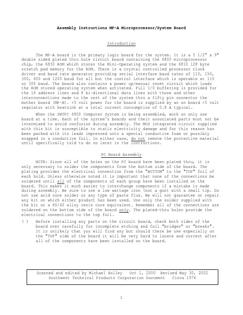
Assembly Instructions MP-A Microprocessor/System BoardIntroductionThe MP-A board is the primary logic board for the system. It is a 5 1/2” x 9" double sided plated thru hole circuit board containing the 6800 microprocessor chip, the 6830 ROM which stores the Mini-Operating system and the 6810 128 byte scratch pad memory for the ROM. There is a crystal controlled processor clockdriver and baud rate generator providing serial interface baud rates of 110, 150, 300, 600 and 1200 baud for all but the control interface which is operable at 110or 300 baud. The board also contains a power up/manual reset circuit which loadsthe ROM stored operating system when activated. Full I/0 buffering is provided for the 16 address lines and 8 bi-directional data lines with those and other interconnections made to the rest of the system thru a fifty pin connector the mother board (MP-B). +5 volt power for the board is supplied by an on board +5 volt regulator with heatsink at a total current consumption of 0.8 A typical.When the SWTPC 6800 Computer System is being assembled, work on only one board at a time. Each of the system's boards and their associated parts must not be intermixed to avoid confusion during assembly. The MOS integrated circuit supplied with this kit is susceptible to static electricity damage and for this reason has been packed with its leads impressed onto a special conductive foam or possibly wrapped in a conductive foil. In either case, do not remove the protective material until specifically told to do so later in the instructions.PC Board AssemblyNOTE: Since all of the holes on the PC board have been plated thru, it isonly necessary to solder the components from the bottom side of the board. The plating provides the electrical connection from the "BOTTOM" to the "TOP" foil of each hold. Unless otherwise noted it is important that none of the connections be soldered until all of the components of each group have been installed on the board. This makes it much easier to interchange components if a mistake is made during assembly. Be sure to use a low wattage iron (not a gun) with a small tip. Do not use acid core solder or any type of paste flux. We will not guarantee or repair any kit on which either product has been used. Use only the solder supplied withthe kit or a 60/40 alloy resin core equivalent. Remember all of the connections are soldered on the bottom side of the board only. The plated-thru holes provide the electrical connections to the top foil.( ) Before installing any parts on the circuit board, check both sides of the board over carefully for incomplete etching and foil "bridges" or "breaks".It is unlikely that you will find any but should there be one especially on the "TOP" side of the board it will be very hard to locate and correct after all of the components have been installed on the board.( ) Attach the resistors to the board. As with all other components, unless noted, use the parts list and component layout drawing to locate each partand install from the "TOP" side of the board bending the leads along the"BOTTOM" side of the board and trimming so that 1/16" to 1/8" of wireremains. Solder. You should have one lM ohm resistor left over.( ) Install all of the capacitors on the board. Be sure to orient the electrolytic capacitors correctly. The polarity is indicated on the component layout drawing. Solder.( ) Install the transistors on the board. The transistors must be turned to match the outlines on the component Layout drawing. Solder.( ) Attach crystal XTAL1 to the circuit board. It should be oriented so its length lies flat across the circuit board as shown in the outline on thecomponent layout drawing. If the crystal has long thin wire leads, they may be bent down 90 degrees at the base of the crystal so they fit into the two holes provided for the crystal on the circuit board. If the crystal has short heave wire leads, solder onto and at a 90 degree angle, the crystal's leads some heavy buss wire. The buss wire with the crystal attached may then heinserted into the board. In either case the crystal must be attached so its metal case could never inadvertently come into contact with either the foil on the circuit board or either one of its own two leads. Solder.( ) Starting from one end of the circuit board install each of the five, 10 pin Molex female edge connectors along; the lower edge of the board. Theseconnectors must he inserted from the "TOP" side of the board and must bepressed down firmly against the hoard. Make sure the body of the connectorseats firmly against the circuit board and that each pin extends completely into the holes on the circuit boars. Not being careful here will cause theboard to either wobble and/or he crooked when plugged onto the mother board.It is suggested that you solder only the two end pins of each of the fiveconnectors until all have been installed at which time if everything looksstraight and rigid you should solder the as yet unsoldered pins.( ) Insert the small nylon indexing plug into the edge connector pin indicated by the small triangular arrow on the "BOTTOM" side of the circuit board. Thisprevents the board from being accidentally plugged onto the mother boardincorrectly.( ) Install integrated circuits IC5 thru IC16 and IC18 thru IC20 on the circuit board. As each one is installed make sure it is down firmly against the board and solder only two of the leads to hold the pack in place while the otherIC’s are being inserted. Be very careful to install each in its correctposition. Do not bend the leads on the back side of the board. Doing so makes it very difficult to remove the integrated circuits should replacement ever be necessary. The semi-circle notch, dot or bar on the end of the package is used for orientation purposes and must match with the outlines shown on the component layout drawing for each of the IC's. After inserting all of theintegrated circuits go back and solder each of the as yet unsoldered pins.( ) Install integrated circuit IC17 on the circuit board. This component must be oriented so its metal face is facing the circuit board with the small metal heatsink sandwiched between the two. The heatsink and IC are secured to the circuit board with a #4-40 x 1/4" screw, lockwasher and nut. The three leads of the integrated circuit must be bent down into each of their respectiveholes and trimmed, and the heatsink must be oriented as shown in thecomponent layout drawing. Solder.( ) Attach the two zero force integrated circuit sockets to board in the ICI and IC2 positions only. The 40 pin socket goes in the IC1 position while the 24 pin socket goes in the IC2 position. Orient each socket so the corner having the projecting tab is adjacent the pin indicated by the "dot" within theintegrated circuit outline on the component layout drawing. Solder.NOTE: MOS integrated circuits are susceptible to damage by staticelectricity. Although some degree of protection is provided internally within the integrated circuits, their cost demands the utmost in care. Before opening and/or installing any MOS integrated circuits you should ground your body and all metallic tools coming into contact with the leads, thru a 1 M ohm 1/4 watt resistor(supplied with the kit). The ground must be an "earth" ground such as a water pipe, and not the circuit board ground. As for the connection to your body, attach a clip lead to your watch or metal ID bracelet. Make absolutely sure you have the 1 Meg ohm resistor connected between you and the "earth" ground, otherwise you will be creating a dangerous shock hazard. Avoid touching the leads of the integrated circuits any more than necessary when installing them, even if you are grounded. On those MOS IC's being soldered in place, the tip of the soldering iron should be grounded as well (separately from your body ground) either with or without a 1 Meg ohm resistor. Most soldering irons having a three prong line cord plug already have a grounded tip. Static electricity should be an important consideration in cold,dry environments. It is less of a problem when it is warm and humid.( ) Install MOS integrated circuits IC3 and IC4 following the precautions given in the preceding section. As it is installed, make sure it is down firmlyagainst the board before soldering all of its leads. Do not bend the leads on the back side-of the board. Doing so makes it very difficult to remove theintegrated circuit should replacement ever be necessary. The "dot" or "notch"on the end of the package is used for orientation purposes and must matchwith that shown on the component layout drawing for the IC.( ) Working from the "TOP" side of the circuit board, fill in all of the feed thru's with molten solder. The feed-thru's are those unused holes on theboard whose internal plating connects the "TOP" and "BOTTOM" circuitconnections. Filling these feed-thru's with molten solder guarantees theintegrity of the connections and increases the current handling capability.( ) Now that all of the components have been installed on the board, double check to make sure all have been installed correctly in their proper location. ( ) Check very carefully to make sure that all connections have been soldered. It is very easy to miss some connections when soldering which can really cause some hard to find problems later during checkout. Also look for solder"bridges" and "cold" solder joints which are another common problem.This completes the assembly phase for the MP-A board. Integrated circuits ICI and IC2 should not be installed until the board goes thru a preliminary checkout detailed in the System Checkout Instructions supplied with the MP-B mother board kit. The System Checkout Instruction are used after having assembled the MP-A Microprocessor/System Board, MP-B mother board, MP-C serial, control interface, and the MP-P power supply.Since the MP-A circuit board now contains MOS devices it is susceptible to damage from severe static electrical sources. One should avoid handling the board any more than necessary and when you must, avoid touching or allowing anything to come into contact with any of the conductors on the board.How It WorksThe entire 6800 Computer System is built around IC1, the 6800 Microprocessor Unit (MPU). Most of the components within the system are used to provide the clocks, buffering and decoding necessary to interface to this integrated circuit. Complete details of the operation and specifications of IC1 are contained in the 6800 Hardware section of the System Documentation Notebook and will not be repeated here.Integrated circuit IC2 is a 1024 x 8 bit read only memory (ROM) which permanently stores the computer's mini-operating system described in the Operating System section of the System Documentation Notebook. Whenever the computer systemis first powered up or when the front panel RESET switch is depressed the computer jumps to this operating system firmware (programming stored in ROM) which gives the user terminal control. Since the mini-operating system uses only 512 words of the ROM, the upper 512 words have been disabled from access and the ROM operating system addresses have been located from E000 to E1FF inclusive.The ROM stored mini-operating requires a small amount of random access memory (RAM) for operation. It uses IC3, a 128 x 8 bit static memory. What is nice here is that a large portion of the RAM memory addresses are unassigned which means many short programs such as the diagnostics can be loaded right into the operating system RAM without using any of the large MP-M static memory cards. Complete information regarding the unassigned RAM locations is contained in the Operating System section of the System Documentation Notebook.IC4 is the crystal controlled clock/baud rate generator. It produces the five baud rate clock frequencies required by the control and serial interfaces. It also generates a clock which is divided by two by half of IC20, split into twonon-overlapping phases by IC18 and IC19 buffered by transistors Q1 thru Q4 and sent onto IC1, the MPU chip. IC14 provides the buffering for each of the used outputs on baud rate generator IC4.Timer integrated circuit IC11 is responsible for generating the power up/ manual pushbutton RESET which loads the mini-operating system stored in the ROM,IC2.Half of D flip flop, IC20 is used for timed halting of the processor indirect memory access (DMA) applications.Integrated circuits ICS, IC6 and IC7 are used as non-inverting address line buffers for each of the sixteen address lines. Integrated circuits IC8 and IC9 are inverting bi-directional transceiver buffers for the system's eight bi-directional data lines. The gates feeding the enable lines of the transceiver IC's guaranteethe appropriate receive or transmit data buss buffers are enabled at the proper time.+5 VDC power for the board is supplied by voltage regulator IC17.Parts List MP-A Microprocessor/System BoardResistorsR1, R2, R4 1M ohm 1/4 watt resistorR3, R7, R12, R13 10K ohm 1/4 watt resistorR5, R6 6.8K ohm 1/4 watt resistorR8, R9, R19 1K ohm 1/4 watt resistorR10, R11 4.7K ohm 1/4 watt resistorR14, R17 10 ohm 1/4 watt resistorR15, R16 22 ohm 1/4 watt resistorR18 470 ohm 1/4 watt resistorCapacitorsC1, C2, C4, C14, C15 0.1 mfd disc. capacitorC3 100 mfd @15 VDC electrolytic capacitor C5 0.01 mfd mylar capacitorC6 0.1 mfd mylar capacitorC7 0.47 mfd tantalum capacitorC8 1000 pF polystyrene capacitorC9, C10 33 pfd polystyrene capacitorC11, C12 120 pfd polystyrene capacitorC13 1000 pfd polystyrene capacitorSemiconductorsIC-1 MC6800 MPU (MOS)IC-2 MC6830L7 ROM (MOS)IC-3 MC6810L-1 RAM (MOS)IC-4 MC14411 Baud Rate Generator (MOS)IC-5, IC-6, IC-7 DM8097 Hex Tri-State BufferIC-8, IC9 DM8835 Quad Bi-directional Transceiver IC-10 7404 Hex InverterIC-11 555 or 1455 TimerIC-12, IC-13 7400 Quad NAND gateIC-14 74L04 HP Hex InverterIC-15 DM8098 Hex Tri-State BufferIC-16 7420 Dual 4-Input MAND GateIC-17 7805 +5 VDC Voltage RegulatorIC-18 74H00 HS Quad NAND GateIC-19 74H08 HS Quad AND GateIC-20 7474 Dual "D" Flip-FlopQ1, Q2 2N5087 transistorQ3, Q4 2N5210 transistorMisc.XTAL 1 1.7971 MHz Parallel Resonant Crystal。
安利4K HD MPX摄像头用户手册说明书

1. Dans le mode de visionnement en direct, double-cliquer sur le canal sur lequel la caméra est connectée pour l’ouvrir en mode plein écran.
2. Passez la souris près du haut du canal où la caméra est connectée et cliquez
bloc d’alimentation non stabilisée et non conforme peut endommager le produit et annuler la garantie. • N’utilisez que le bloc d’alimentation stabilisée fourni avec le produit. L’utilisation de tout autre bloc d’alimentation peut endommager le produit et annuler la garantie. • Le câble fourni est conçu uniquement pour un montage en surface (type CM). Les câbles pour installations encastrées et verticales sont vendus séparément (type CMR). Ces câbles ainsi que d’autres types de câbles sont offerts sur .
CAcotnivneerclatifnognctthioenCaaudmioedraesla caméra
pac-2700wa参数 -回复

pac-2700wa参数-回复PAC2700WA参数- 了解高性能航空电子产品引言:在如今的航空业中,高性能航空电子产品扮演着至关重要的角色。
这些产品的质量和性能直接关系到飞机的安全性和效率。
其中,PAC2700WA 是一款备受推崇的航空电子产品。
本文将详细介绍PAC2700WA的参数和特点,帮助读者全面了解这一高性能产品。
第一部分:PAC2700WA的概述PAC2700WA是一款机载航空电子装备,专为商用飞机而设计。
它由技术先进的电子元件组成,具有高度自动化、稳定性强和可靠性高等特点。
它的出现使飞行员和机组人员在飞行操作过程中获得了更多的信息和支持,提高了航空运输的安全性和效率。
第二部分:技术参数1. 外观尺寸:PAC2700WA的外观尺寸为*(填入具体数值),体积小巧,重量轻。
这种小巧的设计为飞机航行提供了更多的空间,使得其他重要机载设备也能同时安装。
2. 显示屏:PAC2700WA配备了高分辨率的液晶显示屏,使信息更加清晰可见。
这个显示屏可以同时显示多种信息,如飞行速度、高度、航线、气象状况等。
3. 接口:PAC2700WA具有多种标准接口,可以与飞机系统的其他部分进行连接。
这些接口支持数据的输入和输出,以及与其他机载设备的通信。
通过与其他系统的连接,PAC2700WA可以实时获取飞机状态和运行数据,对飞行员和机组人员提供必要的信息。
4. 耐用性:PAC2700WA采用了高质量的材料和结构,具有较强的抗震、抗振和抗温度变化能力。
这使得设备可以在各种恶劣的环境条件下正常工作,保证飞行过程中的安全性和稳定性。
5. 功能:PAC2700WA具有众多的功能特点,其中包括:- 自动化控制系统:PAC2700WA能够自动调整飞机的姿态和飞行状态,在飞行员操作时提供支持和辅助。
- 数据记录与分析:PAC2700WA可以记录飞行过程中的各项数据,并进行后续的数据分析,为飞机维护和改进提供参考。
- 通信功能:PAC2700WA可以与地面控制中心和其他飞机进行通信,提供实时的交流和信息共享。
LX730A培训资料

为了避免故障的发生,需要采取一些预防措施,如定期检查和保养、及时更新和修复漏洞、避免超负荷使用等。
故障预防
06
lx730a案例分析
Chapter
应用案例一
案例名称:lx730a在医疗影像处理中的应用
背景介绍:随着医疗技术的发展,医疗影像处理的需求日益增加。lx730a凭借其强大的处理能力,在此领域发挥重要作用。
lx730a在医疗影像处理中表现出色,其高效的图像处理算法和强大的计算能力,能够快速处理大量的医学影像数据,提高诊断的准确性和效率。此外,其丰富的接口可以方便地与其他医疗设备连接,实现数据的快速传输和共享。
在智能交通领域,lx730a能够实时处理大量的交通数据,包括车辆位置、速度、道路状况等。通过高效的算法和强大的计算能力,它能快速分析数据并提供准确的交通信息,帮助实现交通流量的合理分配和拥堵的缓解。此外,其可靠的数据传输能力和低功耗特性也使其在智能交通领域得到广泛应用。
它集成了最新的5G调制解调技术,支持5G NR/LTE-TDD/LTE-FDD/WCDMA/GSM多模通信。
LX730A具有体积小、重量轻、功耗低等特点,适用于各种工业设备、智能终端等。
多模通信
LX730A支持5G NR/LTE-TDD/LTE-FDD/WCDMA/GSM多模通信,可适应不同的网络环境和需求。
03
用户界面
02
01
基本操作
进阶操作
网络设置
通过分配器或拼接处理器,实现多画面显示。
多画面显示
远程管理
安全功能
01
02
04
03
设备支持密码保护,防止未经授权的操作。
进入菜单,选择网络设置,连接无线网络或有线网络。
- 1、下载文档前请自行甄别文档内容的完整性,平台不提供额外的编辑、内容补充、找答案等附加服务。
- 2、"仅部分预览"的文档,不可在线预览部分如存在完整性等问题,可反馈申请退款(可完整预览的文档不适用该条件!)。
- 3、如文档侵犯您的权益,请联系客服反馈,我们会尽快为您处理(人工客服工作时间:9:00-18:30)。
0 to 700 kPa (0 to 100 PSI)High Pressure, Temperature Compensated & Calibrated,Silicon Pressure Sensors
The MPX2700A series device is a silicon piezoresistive pressure sensor providing a highly accurate and linear voltage output — directly proportional to the applied pressure.The sensor is a single monolithic silicon diaphragm with the strain gauge and a thin–film resistor network integrated on–chip. The sensor is laser trimmed for precise span and offset calibration and temperature compensation.Features
•Unique Silicon Shear Stress Strain Gauge •±1.0% Linearity
•Full Scale Span Calibrated to 40 mV •Easy to Use Chip Carrier Package •Basic Element, Single Ported Devices Available Application Examples •Pump/Motor Controllers •Pneumatic Control •Tire Pressure Gauges •Robotics
•Medical Diagnostics •Pressure Switching •Hydraulics
MAXIMUM RATINGS
VOLTAGE OUTPUT versus APPLIED DIFFERENTIAL PRESSURE The differential voltage output of the X–ducer is directly proportional to the differential pressure applied.
The output voltage of the differential or gauge sensor increases with increasing pressure applied to the pressure side (P1) relative to the vacuum side (P2). Similarly, output voltage increases as increasing vacuum is applied to the vacuum side (P2) relative to the pressure side (P1).
Figure 1 shows a block diagram of the internal circuitry on the stand–alone pressure sensor chip.
X–ducer is a trademark of Motorola, Inc.
Order this document
by MPX2700A/D
MOTOROLA
SEMICONDUCTOR TECHNICAL DATA
元器件交易网。