P187TG5-14V-T中文资料
13745资料

TOP VIEW GND NC VIN VIN BOOST FB/SENSE NC GND 1 2 3 4 5 6 7 8
LT1374CFE LT1374IFE
FE16 PACKAGE 16-LEAD PLASTIC TSSOP
θJA = 40°C/ W EXPOSED PAD SOLDERED TO GROUND PLANE
VOUT = 5V VIN = 10V L = 10µH
1374 TA02
U
1374fb
1
元器件交易网
LT1374
ABSOLUTE
AXI U
RATI GS
Input Voltage LT1374 ............................................................... 25V LT1374HV .......................................................... 32V BOOST Pin Voltage ................................................. 38V BOOST Pin Above Input Voltage ............................. 15V SHDN Pin Voltage ..................................................... 7V BIAS Pin Voltage ...................................................... 7V FB Pin Voltage (Adjustable Part) ............................ 3.5V
常用二极管型号及参数大全

1.塑封整流二极管序号型号 IF VRRM VF Trr 外形A V V μs1 1A1-1A7 1A 50-1000V 1.1 R-12 1N4001-1N4007 1A 50-1000V 1.1 DO-413 1N5391-1N5399 1.5A 50-1000V 1.1 DO-154 2A01-2A07 2A 50-1000V 1.0 DO-155 1N5400-1N5408 3A 50-1000V 0.95 DO-201AD6 6A05-6A10 6A 50-1000V 0.95 R-67 TS750-TS758 6A 50-800V 1.25 R-68 RL10-RL60 1A-6A 50-1000V 1.09 2CZ81-2CZ87 0.05A-3A 50-1000V 1.0 DO-4110 2CP21-2CP29 0.3A 100-1000V 1.0 DO-4111 2DZ14-2DZ15 0.5A-1A 200-1000V 1.0 DO-4112 2DP3-2DP5 0.3A-1A 200-1000V 1.0 DO-4113 BYW27 1A 200-1300V 1.0 DO-4114 DR202-DR210 2A 200-1000V 1.0 DO-1515 BY251-BY254 3A 200-800V 1.1 DO-201AD16 BY550-200~1000 5A 200-1000V 1.1 R-517 PX10A02-PX10A13 10A 200-1300V 1.1 PX18 PX12A02-PX12A13 12A 200-1300V 1.1 PX19 PX15A02-PX15A13 15A 200-1300V 1.1 PX20 ERA15-02~13 1A 200-1300V 1.0 R-121 ERB12-02~13 1A 200-1300V 1.0 DO-1522 ERC05-02~13 1.2A 200-1300V 1.0 DO-1523 ERC04-02~13 1.5A 200-1300V 1.0 DO-1524 ERD03-02~13 3A 200-1300V 1.0 DO-201AD25 EM1-EM2 1A-1.2A 200-1000V 0.97 DO-1526 RM1Z-RM1C 1A 200-1000V 0.95 DO-1527 RM2Z-RM2C 1.2A 200-1000V 0.95 DO-1528 RM11Z-RM11C 1.5A 200-1000V 0.95 DO-1529 RM3Z-RM3C 2.5A 200-1000V 0.97 DO-201AD30 RM4Z-RM4C 3A 200-1000V 0.97 DO-201AD2.快恢复塑封整流二极管序号型号 IF VRRM VF Trr 外形A V V μs(1)快恢复塑封整流二极管1 1F1-1F7 1A 50-1000V 1.3 0.15-0.5 R-12 FR10-FR60 1A-6A 50-1000V 1.3 0.15-0.53 1N4933-1N4937 1A 50-600V 1.2 0.2 DO-414 1N4942-1N4948 1A 200-1000V 1.3 0.15-0.5 DO-415 BA157-BA159 1A 400-1000V 1.3 0.15-0.25 DO-416 MR850-MR858 3A 100-800V 1.3 0.2 DO-201AD7 EU1-EU2 0.25A-1A 100-1000V 1.3 0.4 DO-418 20DF1-20DF10 2A 100-1000V 1.3 0.2 DO-159 30DF1-30DF10 3A 100-1000V 1.3 0.2 DO-201AD10 RU1-RU4 0.25A-3A 100-1000V 1.3 0.411 ERA22-02~10 0.5A 200-1000V 1.3 0.4 R-112 ERA18-02~10 0.8A 200-1000V 1.3 0.4 R-113 ERB43-02~10 0.5A 200-1000V 1.3 0.4 DO-4114 ERB44-02~10 1A 200-1000V 1.3 0.4 DO-1515 ERC18-02~10 1.2A 200-1000V 1.3 0.4 DO-1516 ERD28-02~10 1.5A 200-1000V 1.3 0.4 DO-201AD17 ERD29-02~10 2.5A 200-1000V 1.3 0.4 DO-201AD18 ERD32-02~10 3A 200-1000V 1.3 0.4 DO-201AD19 ERD09-13~15 3A 1300-1500V 1.5 0.6 R-5(2)SK、2CG系列快恢复整流二极管1 SK1-02~30 1.5A 200-3000V 1.3-4 0.5-1 DO-152 SK2-02~30 1A 200-3000V 1.3-4 0.5-1 DO-413 SK3-02~30 2A 200-3000V 1.3-4 0.5-1 DO-154 SK4-02~30 0.5A 300-3000V 1.3-4 0.5-1 DO-415 2CG04-2CG30 0.2A 300-3000V 1.3-4 0.5-1 DO-41 (3)快恢复塑封阻尼二极管1 2CN1-2CN1C 1A 200-1200V 1.32 DO-412 2CN2D-2CN2M 0.5A 200-1000V 1.3 2 DO-413 2CN3D-2CN3M 1A 200-1000V 1.3 6 DO-414 2CN4D-2CN4M 1.5A 200-1000V 1.3 0.8 DO-155 2CN5D-2CN5M 1.5A 200-1000V 1.0 1 DO-156 2CN6D-2CN6M 1A 200-1000V 1.3 6 DO-417 2CN12D-2CN12M 3A 200-1000V 1.3 1 DO-201AD8 RH1Z-RH1C 0.6A 200-1000V 1.3 4 DO-419 TVR4J-TVR4N 1.2A 600-1000V 1.2 20 DO-153.超高频塑封二极管1 ERA34-10 0.1A 1000V 3 0.15 R-12 ERA32-02~10 1A 200-1000V 1.3 0.1 DO-413 ERB32-02~10 1.2A 200-1000V 1.3 0.1 DO-154 ERC30-02~10 1.5A 200-1000V 1.3 0.1 DO-155 ERC32-02~10 3A 200-1000V 1.3 0.1 DO-201AD6 EG01E-EG01C 0.5A 200-1000V 2 0.1 DO-417 EG1E-EG1C 1A 200-1000V 1.8 0.1 DO-418 RG10Z-RG10C 1.2A 200-1000V 2 0.1 DO-159 RG2Z-RG2C 1.5A 200-1000V 1.8 0.1 DO-1510 RG4Z-RG4C 3A 200-1000V 2 0.1 D0-201AD4.超快恢复塑封二极管序号型号 IF VRRM VF Trr 外形A V V ns(1)超快恢复塑封二极管1 SF10-SF50 1-5A 50-1000V 0.95-1.7 352 SF80-SF160 8-16A 50-600V 0.95-1.4 35 TO-2203 EGP10-EGP50 1-5A 50-200V 1.1 354 ERC38~04-ERC38~10 1A 400-1000V 1.7 50 DO-415 RL2-RL2C 2A 400-1000V 1.7 50 DO-156 RL3-RL3C 3A 400-1000V 1.7 50 DO-201AD7 1H1-1H8 1A 50-1000V 1.1-1.7 50-75 R-18 HER10-HER60 1-6A 50-1000V 1.1-1.7 50-759 HER80-HER160 8-6A 50-1000V 1.1-1.7 50-75 TO-22010 UF10-UF60 1-6A 50-1000V 1.1-1.7 50-7511 EL1Z-EL1 1.5A 200-350V 1.3 50 DO-15(2)MUR超快恢复整流二极管1 MUR120-MUR1120 1A 200-1200V 0.95-1.5 35-50 DO-412 MUR420-MUR4120 4A 200-1200V 0.95-1.6 35-75 DO-201AD3 MUR820-MUR8120 8A 200-1200V 1.3-2.1 35-75 TO-220AC4 MUR1020-MUR10120 10A 200-1200V 1.3-2.1 35-75 TO-220AC5 MUR1520-MUR15120 15A 200-1200V 1.3-2.1 35-75 TO-220AC6 MUR2020-MUR20120 20A 200-1200V 1.3-2.1 35-75 TO-220AB7 MUR3020-MUR30120 30A 200-1200V 1.3-2.1 35-75 TO-247AD8 MUR6020-MUR60120 60A 200-1200V 1.3-2.1 35-75 TO-247AD (3)RHRP、RHRG超快恢复二极管1 RHRP820-RHRP8120 8A 200-1200V 2.1-3.2 35-70 TO-220AC2 RHRP1520-RHRP15120 15A 200-1200V 2.1-3.2 40-75 TO-220AC3 RHRP3020-RHRP30120 30A 200-1200V 2.1-3.2 45-75 TO-220AC4 RHRG3020-RHRG30120 30A 200-1200V 2.1-3.2 45-75 TO-247AC5 RHRG5020-RHRG50120 50A 200-1200V 2.1-3.2 50-100 TO-247AC6 RHRG6020-RHRG60120 60A 200-1200V 2.1-3.2 45-75 TO-247AD (4)BYV29~79、BYT28~79超快恢复二极管1 BYW29-100~200 8A 100-200V 1.1 25 TO-220AC2 BYV29-300~500 9A 300-500V 1.25 60 TO-220AC3 BYQ28 -100~200 10A 100-200V 1.1 20 TO-220AB4 BYT28-300~500 10A 300-500V 1.4 60 TO-220AB5 BYV79-100~200 14A 100-200V 1.3 30 TO-220AC6 BYT79-300~500 14A 300-500V 1.4 60 TO-220AC7 BYV32-100~200 20A 100-200V 1.1 25 TO-220AB8 BYV34-300~500 20A 300-500V 1.1 60 TO-220AB9 BYV42-100~200 30A 100-200V 1.1 28 TO-220AB10 BYV44-300~500 30A 300-500V 1.25 60 TO-220AB5.肖特基整流二极管序号型号 IF VRRM VF 外形A V V(1)肖特基塑封整流二极管1 1N5817-1N5819 1A 20-40V 0.45-0.6 DO-412 1N5820-1N5822 3A 20-40V 0.45-0.6 DO-201AD3 SRT12-SRT100 1A 20-100V 0.55-0.85 R-14 SR10-SR50 1-5A 20-100V 0.55-0.855 SB120-SB1B0 1A 20-100V 0.55-0.85 DO-416 SB220-SB2B0 2A 20-100V 0.55-0.85 DO-157 SB320-SB3B0 3A 20-100V 0.55-0.85 DO-201AD8 SB520-SB5B0 5A 20-100V 0.55-0.85 D0-201AD9 ERA81-002~009 1A 20-90V 0.55-0.9 DO-4110 ERB81-002~009 2A 20-90V 0.55-0.9 DO-1511 ERC81-002~009 3A 20-90V 0.55-0.9 DO201AD12 EK03-EK09 1A 20-90V 0.55-0.81 DO-4113 EK13-EK19 1.5A 20-90V 0.55-0.81 DO-1514 EK33-EK39 2A 20-90V 0.55-0.81 DO-1515 EK43-EK49 3A 20-90V 0.55-0.81 DO-201AD(2)MBR、PBYR系列大电流肖特基整流二极管1 MBR1020-MBR1060 10A 20-60V 0.57-0.8 TO-220AC2 MBR1620-MBR1660 16A 20-60V 0.57-0.8 TO-220AC3 MBR2020CT-2060CT 20A 20-60V 0.57-0.8 TO-220AB4 MBR2520CT-2560CT 25A 20-60V 0.57-0.8 TO-220AB5 MBR3020PT-3060PT 30A 20-60V 0.57-0.8 TO-247AD6 MBR4020PT-4060PT 40A 20-60V 0.57-0.8 TO-247AD7 MBR6020PT-6060PT 60A 20-60V 0.57-0.8 TO-247AD8 PBYR735-745 7A 20-45V 0.56-0.66 TO-220AC9 PBYR1020-1060 10A 20-60V 0.56-0.77 TO-220AC10 PBYR1635-1660 16A 20-60V 0.56-0.77 TO-220AC11 PBYR2020CT-2045CT 20A 20-45V 0.56-0.65 TO-220AB12 PBYR3035PT-3060PT 30A 20-60V 0.56-0.77 TO-247AD 6.玻球快恢复二极管、玻钝芯片塑封二极管序号型号 IF VRRM VF Trr 外形A V V ns(1)BYV、BYT、BYM、BYW玻球快恢复二极管1 BYV26A-BYV26E 1A 200-1000V 1.5 0.03 DO-204AP2 BYV12-BYV16 1.5A 100-1000V 1.5 0.3 DO-204AP3 BYV96A-BYV96E 1.5A 100-1000V 1.5 0.3 DO-204AP4 BYV27-50~200 2A 50-200V 1.1 0.025 DO-204AP5 BYV28-50~200 3.5A 50-200V 1.1 0.03 G36 BYT52A-BYT52M 1A 50-1000V 1.3 0.2 DO-204AP7 BYT54A-BYT54M 1.25A 50-1000V 1.5 0.1 DO-204AP8 BYT53A-BYT53M 1.5A 50-1000V 1.1 0.05 DO-204AP9 BYT56A-BYT56M 3A 200-1000V 1.4 0.1 G310 BYM26A-BYM26M 2.3A 200-1000V 1.5 0.03 G311 BYM36A-BYM36M 3A 200-1000V 1.1 0.15 G312 BYW32-BYW38 2A 200-1000V 1.1 0.2 DO-204AP13 BYW52-BYW56 2A 200-1000V 1.1 4 DO-204AP14 BYW72-BYW76 3A 200-600V 1.1 0.2 G315 BYW96A-BYW96E 3A 200-1000V 1.5 0.2 G316 BY228 3A 1500V 1.5 20 G3(2)GP、RGP系列玻钝芯片塑封二极管17 GP10-GP30 1-3A 50-1000V 1.118 RGP01-10~RGP01-20 0.1A 1000-2000V 2 0.2-0.5 DO-4119 RGP05-10~RGP05-20 0.5A 1000-2000V 2 0.2-0.5 DO-4120 RGP10-RGP60 1-6A 50-2000V 1.3 0.15-0.57.PD、TR、PR系列高压塑封二极管1 PD0112-PD0160 0.1A 1200-6000V 1.2-5 DO-412 PD0312-PD0360 0.3A 1200-6000V 1.2-5 DO-153 PD0512-PD0560 0.5A 1200-6000V 1.2-5 DO-154 PD112-PD130 1A 1200-3000V 1.2-4 DO-155 PD1512-PD1530 1.5A 1200-3000V 1.2-4 DO-156 PD212-PD220 2A 1200-2000V 1.2-2.5 DO-201AD7 PD312-PD320 3A 1200-2000V 1.2-2.5 DO-201AD8 PD612-PD620 6A 1200-2000V 1.2-2.5 R-69 TR0112-TR0160 0.1A 1200-6000V 1.5-8 0.5-0.8 DO-4110 TR0312-TR0360 0.3A 1200-6000V 1.5-8 0.5-0.8 DO-1511 TR0512-TR0560 0.5A 1200-6000V 1.5-8 0.5-0.8 DO-1512 TR112-TR130 1A 1200-3000V 1.5-6 0.5-0.8 DO-1513 TR1512-TR1530 1.5A 1200-3000V 1.5-6 0.5-0.8 DO-1514 TR212-TR220 2A 1200-2000V 1.5-2.7 0.5-0.8 DO-201AD15 TR312-TR320 3A 1200-2000V 1.5-2.7 0.5-0.7 DO-201AD16 TR612-TR620 6A 1200-2000V 1.5-2.7 0.5-0.8 R-617 PR01-PR1 0.1-1A 1200-3000V 1.5-4 0.1-0.5 DO-1518 RC2 0.3A 2000V 3 0.5 DO-4119 RU4D-RP3F 1.5A-2A 1300-1500V 1.5 0.3 DO-201AD8.稳压二极管序号名称型号 PZM VZW V稳压二极管1 BZX55 0.5W 2.4V-47V2 1N5985B~1N6031B 0.5W 2.4V-200V3 1N4728~1N4764 1W 3.3V-100V4 1N5911B~1N5956B 1.5W 2.7V-200V5 2CW37-2.4~36 0.5W 2.4V-36V6 2CW51-2CW68 0.25W 3V-28.5V7 2CW101-2CW121 1W 3V-37.5V8 2DW50-2DW64 1W 41V-190V9 2DW80-2DW190 3W 41V-190V10 2DW110-2DW151 10W 4.3V-470V11 2DW170-2DW202 50W 4.3V-200V12 温度补偿稳压二极管 2DW230-2DW236 0.2W 5.8V-6.6V9.高速开关二极管序号型号 IC VRM Trr 外形mA V ns1 1N4148 150 100V 4 DO-352 1N4149-1N4154 150 35-100V 2-4 DO-353 1N4446-1N4454 150 40-100V 1-4 DO-354 1N914 75 100V 4 DO-355 BAV17-BAV21 250 25-250V 50 DO-356 BAW75-BAW76 300 35-75V 4 DO-357 2CK70-2CK79 10-280 20-60V 3-10 DO-358 2CK80-2CK85 10-300 20-60V 5-10 DO-359 1S1553-1S1555 100 70-35V 3 DO-3510 1S2471-1S2473 130-110 90-40V 3 DO-35几种常用二极管的特点1.整流二极管整流二极管结构主要是平面接触型,其特点是允许通过的电流比较大,反向击穿电压比较高,但PN结电容比较大,一般广泛应用于处理频率不高的电路中。
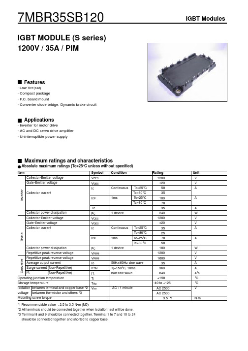
7MBR35SB120中文资料
IRRM R
B
VCE=1200V, VGE=0V VCE=0V, VGE=±20V VCE=20V, IC=35mA VGE=15V, Ic=35A chip
terminal VGE=0V, VCE=10V, f=1MHz VCC=600V IC=35A VGE=±15V RG=33Ω
元器件交易网
7MBR35SB120
IGBT MODULE (S series) 1200V / 35A / PIM
IGBT Modules
Features
· Low VCE(sat) · Compact package · P.C. board mount · Converter diode bridge, Dynamic brake circuit
Unit V V A
A
A W V V A
A
W V V A A A2s °C °C V
N·m
元器件交易网 IGBT Modules
7MBR35SB120
Electrical characteristics (Tj=25°C unless otherwise specified)
Collector current : Ic [ A ]
[ Inverter ] Collector current vs. Collector-Emitter voltage
Tj= 25 oC (typ.) 80
VGE= 20V 15V 12V
60
10V 40
[ Inverter ] Collector current vs. Collector-Emitter voltage
Item Collector-Emitter voltage Gate-Emitter voltage
MM5Z16VT1G稳压二极管规格书
Zener Voltage Regulators150mW SOD–523Surface MountWe declare that the material of product compliance with RoHS requirements.ORDERING INFORMATIONDevice Package Shipping MM5ZXXXT1GSOD-5233000/Tape&ReelThis series of Zener diodes is packaged in a SOD–523surface mount package that has a power dissipation of 100mW.They are designed to provide voltage regulation protection and are especially attractive in situations where space is at a premium.They are well suited for applications such as cellular phones,hand held portables,and high density PC boards.Specification Features:•Standard Zener Breakdown Voltage Range –2.4V to 75V •Steady State Power Rating of 200mW•Small Body Outline Dimensions:0.047"x 0.032"(1.20mm x 0.80mm)•Low Body Height:0.028"(0.7mm)•ESD Rating of Class 3(>16kV)per Human Body ModelMechanical Characteristics:CASE:Void-free,transfer-molded,thermosetting plastic Epoxy Meets UL 94V-0LEAD FINISH:100%Matte Sn (Tin)QUALIFIED MAX REFLOW TEMPERATURE:260°C Device Meets MSL 1Requirements MOUNTING POSITION:AnyMAXIMUM RATINGSRatingSymbol Max Unit Total Device Dissipation FR−5Board,P D150mW@T A =25︒C Junction and Storage T J,Tstg−65to ︒CTemperature Range+150Maximum ratings are those values beyond which devicedamage can occur.Maximum ratings applied to the device are individual stress limit values (not normal operating conditions)and are not valid simultaneously.If these limits are exceeded,device functional operation is not implied,damage may occur and reliability may be affected.MM5Z2V4T1G SERIES12CATHODE ANODEMARKING DIAGRAMxx dxx=Specific Device Code d =Date CodeSOD–523MM5Z2V4T1G SERIES ELECTRICAL CHARACTERISTICS I(T A=25︒C unless otherwise noted,I FV F=0.9V Max.@I F=10mA for all types)Symbol ParameterVZ Reverse Zener Voltage@I ZT IZT Reverse Current VZVRVZ ZT Maximum Zener Impedance@I I R VFZT IZTIZK Reverse CurrentZZK Maximum Zener Impedance@I ZKIR Reverse Leakage Current@V RV R Reverse VoltageI F Forward Current Zener Voltage Regulator V F Forward Voltage@I FQV Z Maximum Temperature Coefficient of V ZC Max.Capacitance@V R=0and f=1MHz100(%)80DISS IP ATI ON 60 40POWER20255075100125150TEMPERATURE(︒C)Figure1.Steady State Power Derating MM5Z2V4T1G SERIESELECTRICAL CHARACTERISTICS (T A =25︒C unless otherwise noted,V F =0.9V Max.@I F =10mA for all types)Zener Voltage (Note 1)Zener Impedance Leakage CurrentQ V Z C ZZT(mV/k)@V =0V(Volts)@I@I ZT Z@II @VRZZKR@IZTf =1MHzDevice ZTZKRDevice Marking Min Nom Max mA W W mA m A Volts Min Max pF MM5Z2V4T1G 00 2.2 2.4 2.651001000 1.050 1.0−3.50450MM5Z2V7T1G 01 2.5 2.7 2.951001000 1.020 1.0−3.50450MM5Z3V0T1G 02 2.8 3.0 3.251001000 1.010 1.0−3.50450MM5Z3V3T1G 05 3.1 3.3 3.55951000 1.05 1.0−3.50450MM5Z3V6T1G 06 3.4 3.6 3.85901000 1.05 1.0−3.50450MM5Z3V9T1G 07 3.7 3.9 4.15901000 1.03 1.0−3.5−2.5450MM5Z4V3T1G 08 4.0 4.3 4.65901000 1.03 1.0−3.50450MM5Z4V7T1G 09 4.4 4.7 5.0580800 1.03 2.0−3.50.2260MM5Z5V1T1G 0A 4.8 5.1 5.4560500 1.02 2.0−2.7 1.2225MM5Z5V6T1G 0C 5.2 5.6 6.0540400 1.01 2.0−2.0 2.5200MM5Z6V2T1G 0E 5.8 6.2 6.6510100 1.03 4.00.4 3.7185MM5Z6V8T1G 0F 6.4 6.87.2515160 1.02 4.0 1.2 4.5155MM5Z7V5T1G 0G 7.07.57.9515160 1.01 5.0 2.5 5.3140MM5Z8V2T1G 0H 7.78.28.7515160 1.00.7 5.0 3.2 6.2135MM5Z9V1T1G 0K 8.59.19.6515160 1.00.27.0 3.87.0130MM5Z10VT1G 0L 9.41010.6520160 1.00.18.0 4.58.0130MM5Z11VT1G 0M 10.41111.6520160 1.00.18.0 5.49.0130MM5Z12VT1G 0N 11.41212.752580 1.00.18.0 6.010130MM5Z13VT1G 0P 12.413.2514.153080 1.00.18.07.011120MM5Z15VT1G 0T 14.31515.8530200 1.00.0510.59.213110MM5Z16VT1G 0U 15.316.217.1240200 1.00.0511.210.414105MM5Z18VT1G 0W 16.81819.1245225 1.00.0512.612.416100MM5Z20VT1G 0Z 18.82021.2255225 1.00.0514.014.41885MM5Z22VT1G 1020.82223.3255250 1.00.0515.416.42085MM5Z24VT1G 1122.824.225.6270120 1.00.0516.818.42280MM5Z27VT1G 1225.12728.9280300 1.00.0518.921.425.370MM5Z30VT1G 14283032280300 1.00.0521.024.429.470MM5Z33VT1G 18313335280300 1.00.0523.227.433.470MM5Z36VT1G 19343638290500 1.00.0525.230.437.470MM5Z39VT1G 203739412130500 1.00.0527.333.441.245MM5Z43VT1G 214043461150500 1.00.0530.137.646.640MM5Z47VT1G 1A 4447501170500 1.00.0532.942.051.840MM5Z51VT1G 1C 4851541180500 1.00.0535.746.657.240MM5Z56VT1G 1D 5256601200500 1.00.0539.252.263.840MM5Z62VT1G 1E 5862661215500 1.00.0543.458.871.635MM5Z68VT1G 1F 6468721240500 1.00.0547.665.679.835MM5Z75VT1G1G70757912555001.00.0552.573.488.6351.Zener voltage is measured with a pulse test current I Z at an ambient temperature of 25︒C.MM5Z2V4T1G SERIESSC-79/SOD-523DIMENSIONS (mm are the original dimensions)UNIT A b p c D E H E V m m0.70.350.2 1.30.9 1.70.150.50.250.11.10.71.5Note1.The marking bar indicates the cathode.OUTLINE REFERENCES EUROPEAN ISSUE DATEVERSION IECJEDECEIAJ PROJECTIONSOD523SC-7998-11-25。
EEETG1J470V中文资料(PANASONIC)中文数据手册「EasyDatasheet - 矽搜」

Min. Packaging
Q’ty 回流 大坪
(pcs)
(2) 1000 (2) 1000 (2) 500 (2) 500
10 10.2 G 270 0.30 0.30
(10) (10.2) (G) (270) (0.30) 0.30
12.5 13.5 H13 800 0.12 0.30
(12.5) (13.5) (H13)
芯片中文手册,看全文,戳
n 表壳尺寸VS电容,ESR和纹波电流
电容
(µF)
W.V.
(V) size
10 ESR 20°C -40°C
47
100
E 1.00
20
220
(E) (1.00) (20)
F 0.50
10
330
(F) (0.50) (10)
G 0.30
6.0
470
(G) (0.30) (6.0)
F 1.30
32
(F) (1.30) (32)
G 1.00
25
G 1.00
25
(900) 950 950
涟 当前
70 (70) 90 90
()显示小型化尺寸
后缀:U
H13 0.42
8.4
250
J16 0.30
6.0
350
K16 0.28
5.6
400
K16 0.28
5.6
400
设计,规格时如有变更,恕不另行通知.向工厂购买和/或使用之前,在当前技术规范.如果一个安全性有疑义时本产品,请务必立 即与我们触点.
马克无铅 制品
(Black circle)
Negative polarity marking
LD7535中文资料

LD753511/15/20051Green-Mode PWM Controller with Integrated ProtectionsProduct Spec. (Rev. 00)General DescriptionThe LD7535 is a low cost, low startup current, current mode PWM controller with green-mode power-saving operation. The integrated functions include the leading-edge blanking of the current sensing, internal slope compensation and the tiny package of SOT-26. It would provide the users a superior AC/DC power application of higher efficiency, low external component counts, and lower cost solution for applications.In comparing with the previous generations like LD755X, the LD7535 features more or functions for the following characteristics ---z Add OLP (Over Load Protection) function to providebetter protection performance for fault conditions like short circuit or over load.z Modify the OVP (Over Voltage Protection) mechanismfrom the cycle-by-cycle mode to the hiccup mode.Featuresz High-Voltage CMOS Process with Excellent ESDprotectionz Very Low Startup Current (<20µA) z Current Mode Controlz Non-audible-noise Green Mode Control z UVLO (Under Voltage Lockout)z LEB (Leading-Edge Blanking) on CS Pin z Programmable Switching Frequency z Internal Slope Compensationz OVP (Over Voltage Protection) on Vcc Pin z OLP (Over Load Protection) z 300mA Driving CapabilityApplicationsz Switching AC/DC Adaptor and Battery Charger z Open Frame Switching Power Supply z 384X ReplacementTypical Application查询LD7535供应商绿色模式PWM 控制器具有多种保护功能2Pin ConfigurationDIP-8 (TOP VIEW)SOT-26 (TOP VIEW) YY, Y : Y ear code (D: 2004, E: 2005…..) WW, W : W eek code P : LD75..(Product family code)## : Production code123456GND COMPRTOUTVCCCSY WP 3518 23476 5TOP MARK YYWW##O U TV C CN CC SG N DC O M P N CR TY The PB freed package is identified in embossed font123456WP 35YOrdering InformationPart number Package TOP MARK Shipping LD7535 IL SOT-26YWP/35 3000 /tape & reel LD7535 IN DIP-8LD7535IN 3600 /tube /Carton LD7535 BL SOT-26 (PB free) (*)YWP/35 3000 /tape & reel LD7535 BNDIP-8 (PB free)LD7535BN3600 /tube /Carton(*)printed in different fontPin DescriptionsPIN(SOT-26)NAME FUNCTION1 GND Ground2 COMPVoltage feedback pin (same as the COMP pin in UC384X), By connecting a photo-coupler to close the control loop and achieve the regulation. 3 RTThis pin is to program the switching frequency. By connecting a resistorto ground to set the switching frequency. 4 CS Current sense pin, connect to sense the MOSFET current 5 VCC Supply voltage pin6OUTGate drive output to drive the external MOSFET2-电压反馈引脚乮同COMP 引脚的UC384X•j•C 通过光电耦合器连接丆关闭控制回路丆实现调节3-该引脚为开关频率进行编程。
Altivar 71 ATV71HD15N4Z 变速提供商数据表说明书

i s c l a i me r : T h i s d o c u m e n t a t i o n i s n o t i n t e n d e d a s a s u b s t i t u t ef o r a n d i s n o t t o b e u s e d f o r d e t e r m i n i ng s u i t a b i l i t y o r r e l i a b i l i t y o f th e s e p r o d u c t s f o r s p e ci f i c u s e r a p p l i c a t i o n sProduct datasheetCharacteristicsATV71HD15N4Zvariable speed drive ATV71 - 15kW-20HP - 480V - EMC filter-w/o graphic terminalMainRange of productAltivar 71Product or component type Variable speed driveProduct specific application Complex, high-power machines Component name ATV71Motor power kW 15 kW at 380...480 V 3 phases Motor power hp 20 hp at 380...480 V 3 phases Motor cable length <= 50 m Shielded cable <= 100 m Unshielded cable [Us] rated supply voltage 380...480 V (- 15...10 %)Network number of phases 3 phasesLine current 39 A for 480 V 3 phases 15 kW / 20 hp 48 A for 380 V 3 phases 15 kW / 20 hp EMC filter Integrated Assembly style With heat sinkVariant Without remote graphic terminalApparent power 31.6 kVA at 380 V 3 phases 15 kW / 20 hp Prospective line Isc <= 22 kA, 3 phasesNominal output current 27 A at 4 kHz 460 V 3 phases 15 kW / 20 hp 33 A at 4 kHz 380 V 3 phases 15 kW / 20 hp Maximum transient current 49.5 A for 60 s 3 phases 15 kW / 20 hp 54.5 A for 2 s 3 phases 15 kW / 20 hp Output frequency0.1...599 Hz Nominal switching frequency 4 kHzSwitching frequency1...16 kHz adjustable4...16 kHz with derating factorAsynchronous motor control profileENA (Energy adaptation) system for unbalanced loads Flux vector control (FVC) with sensor (current vector)Sensorless flux vector control (SFVC) (voltage or current vector)Voltage/Frequency ratio (2 or 5 points)Type of polarizationNo impedance for ModbusComplementaryProduct destinationAsynchronous motors Synchronous motorsSupply voltage limits323...528 VSupply frequency50...60 Hz (- 5...5 %)Network frequency47.5...63 HzSpeed range 1...100 for asynchronous motor in open-loop mode, without speed feedback1...50 for synchronous motor in open-loop mode, without speed feedback1...1000 for asynchronous motor in closed-loop mode with encoder feedbackSpeed accuracy+/- 0.01 % of nominal speed for 0.2 Tn to Tn torque variation in closed-loop mode with encoderfeedback+/- 10 % of nominal slip for 0.2 Tn to Tn torque variation without speed feedbackTorque accuracy+/- 15 % in open-loop mode, without speed feedback+/- 5 % in closed-loop mode with encoder feedbackTransient overtorque220 % of nominal motor torque +/- 10 % for 2 s170 % of nominal motor torque +/- 10 % for 60 s every 10 minutesBraking torque<= 150 % with braking or hoist resistor30 % without braking resistorSynchronous motor control profile Vector control without speed feedbackRegulation loop Adjustable PI regulatorMotor slip compensation AdjustableAutomatic whatever the loadNot available in voltage/frequency ratio (2 or 5 points)SuppressableLocal signalling 1 LED red presence of drive voltageOutput voltage<= power supply voltageInsulation Electrical between power and controlType of cable With a NEMA Type1 kit : 3-strand UL 508 cable at 40 °C, copper 75 °C PVCWith an IP21 or an IP31 kit : 3-strand IEC cable at 40 °C, copper 70 °C PVCWithout mounting kit : 1-strand IEC cable at 45 °C, copper 70 °C PVCWithout mounting kit : 1-strand IEC cable at 45 °C, copper 90 °C XLPE/EPRElectrical connection AI1-/AI1+, AI2, AO1, R1A, R1B, R1C, R2A, R2B, LI1...LI6, PWR terminal 2.5 mm² / AWG 14L1/R, L2/S, L3/T, U/T1, V/T2, W/T3, PC/-, PO, PA/+, PA, PB terminal 35 mm² / AWG 2Tightening torque AI1-/AI1+, AI2, AO1, R1A, R1B, R1C, R2A, R2B, LI1...LI6, PWR 0.6 N.mL1/R, L2/S, L3/T, U/T1, V/T2, W/T3, PC/-, PO, PA/+, PA, PB 5.4 N.m / 47.7 lb.inSupply Internal supply for reference potentiometer (1 to 10 kOhm), 10.5 V DC +/- 5 %, <= 10 mA foroverload and short-circuit protectionInternal supply, 24 V DC, voltage limits 21...27 V, <= 200 mA for overload and short-circuit protection Analogue input number2Analogue input type AI1-/Al1+ bipolar differential voltage +/- 10 V DC, input voltage 24 V max, resolution 11 bits + signAI2 software-configurable current 0...20 mA, impedance 242 Ohm, resolution 11 bitsAI2 software-configurable voltage 0...10 V DC, input voltage 24 V max, impedance 30000 Ohm,resolution 11 bitsSampling duration AI1-/Al1+ 2 ms, +/- 0.5 ms for analog input(s)Al2 2 ms, +/- 0.5 ms for analog input(s)LI1...LI5 2 ms, +/- 0.5 ms for discrete input(s)LI6 (if configured as logic input) 2 ms, +/- 0.5 ms for discrete input(s)Response time<= 100 ms in STO (Safe Torque Off)AO1 2 ms, tolerance +/- 0.5 ms for analog output(s)R1A, R1B, R1C 7 ms, tolerance +/- 0.5 ms for discrete output(s)R2A, R2B 7 ms, tolerance +/- 0.5 ms for discrete output(s)Accuracy AI1-/Al1+ +/- 0.6 % for a temperature variation 60 °CAI2 +/- 0.6 % for a temperature variation 60 °CAO1 +/- 1 % for a temperature variation 60 °CLinearity error AI1-/Al1+, AI2 +/- 0.15 % of maximum valueAO1 +/- 0.2 %Analogue output number1Analogue output type AO1 software-configurable current 0...20 mA, impedance 500 Ohm, resolution 10 bitsAO1 software-configurable logic output 10 V <= 20 mAAO1 software-configurable voltage 0...10 V DC, impedance 470 Ohm, resolution 10 bitsDiscrete output number2Discrete output type R1A, R1B, R1C configurable relay logic NO/NC, electrical durability 100000 cyclesR2A, R2B configurable relay logic NO, electrical durability 100000 cyclesMinimum switching current Configurable relay logic 3 mA at 24 V DCMaximum switching current R1, R2 on resistive load, 5 A at 250 V AC, cos phi = 1,R1, R2 on resistive load, 5 A at 30 V DC, cos phi = 1,R1, R2 on inductive load, 2 A at 250 V AC, cos phi = 0.4,R1, R2 on inductive load, 2 A at 30 V DC, cos phi = 0.4,Discrete input number7Discrete input type LI6 : switch-configurable 24 V DC with level 1 PLC, impedance: 3500 OhmPWR : safety input 24 V DC, impedance: 1500 Ohm conforming to ISO 13849-1 level dLI1...LI5 : programmable 24 V DC with level 1 PLC, impedance: 3500 OhmLI6 : switch-configurable PTC probe 0...6, impedance: 1500 OhmDiscrete input logic LI1...LI5 positive logic (source), < 5 V (state 0), > 11 V (state 0)LI1...LI5 negative logic (sink), > 16 V (state 0), < 10 V (state 0)LI6 (if configured as logic input) positive logic (source), < 5 V (state 0), > 11 V (state 0)LI6 (if configured as logic input) negative logic (sink), > 16 V (state 0), < 10 V (state 0) Acceleration and deceleration ramps Automatic adaptation of ramp if braking capacity exceeded, by using resistorLinear adjustable separately from 0.01 to 9000 sS, U or customizedBraking to standstill By DC injectionProtection type Drive against exceeding limit speedDrive against input phase lossDrive break on the control circuitDrive input phase breaksDrive line supply overvoltageDrive line supply undervoltageDrive overcurrent between output phases and earthDrive overheating protectionDrive overvoltages on the DC busDrive short-circuit between motor phasesDrive thermal protectionMotor motor phase breakMotor power removalMotor thermal protectionInsulation resistance> 1 mOhm at 500 V DC for 1 minute to earthFrequency resolution Analog input 0.024/50 HzDisplay unit 0.1 HzCommunication port protocol CANopenModbusConnector type 1 RJ45 for Modbus on front face1 RJ45 for Modbus on terminalMale SUB-D 9 on RJ45 for CANopenPhysical interface2-wire RS 485 for ModbusTransmission frame RTU for ModbusTransmission rate20 kbps, 50 kbps, 125 kbps, 250 kbps, 500 kbps, 1 Mbps for CANopen4800 bps, 9600 bps, 19200 bps, 38.4 Kbps for Modbus on terminal9600 bps, 19200 bps for Modbus on front faceData format8 bits, 1 stop, even parity for Modbus on front face8 bits, odd even or no configurable parity for Modbus on terminalNumber of addresses 1...247 for Modbus1...127 for CANopenMethod of access Slave for CANopenMarking CEOperating position Vertical +/- 10 degreeHeight400 mmDepth213 mmWidth230 mmProduct weight13 kgOption card CC-Link communication cardController inside programmable cardDeviceNet communication cardEthernet/IP communication cardFipio communication cardI/O extension cardInterbus-S communication cardInterface card for encoderModbus Plus communication cardModbus TCP communication cardModbus/Uni-Telway communication cardOverhead crane cardProfibus DP communication cardProfibus DP V1 communication cardEnvironmentNoise level60.2 dB conforming to 86/188/EECDielectric strength3535 V DC between earth and power terminals5092 V DC between control and power terminalsElectromagnetic compatibility Conducted radio-frequency immunity test conforming to IEC 61000-4-6 level 3Electrical fast transient/burst immunity test conforming to IEC 61000-4-4 level 4Electrostatic discharge immunity test conforming to IEC 61000-4-2 level 3Radiated radio-frequency electromagnetic field immunity test conforming to IEC 61000-4-3 level 3Voltage dips and interruptions immunity test conforming to IEC 61000-4-111.2/50 µs - 8/20 µs surge immunity test conforming to IEC 61000-4-5 level 3Standards EN 55011 class A group 2EN 61800-3 environments 1 category C3EN 61800-3 environments 2 category C3EN/IEC 61800-3EN/IEC 61800-5-1IEC 60721-3-3 class 3C1IEC 60721-3-3 class 3S2UL Type 1Product certifications CSAC-TickGOSTNOM 117ULPollution degree 2 conforming to EN/IEC 61800-5-1IP degree of protection IP20 on upper part without blanking plate on cover conforming to EN/IEC 60529IP20 on upper part without blanking plate on cover conforming to EN/IEC 61800-5-1IP21 conforming to EN/IEC 60529IP21 conforming to EN/IEC 61800-5-1IP41 on upper part conforming to EN/IEC 60529IP41 on upper part conforming to EN/IEC 61800-5-1IP54 on lower part conforming to EN/IEC 60529IP54 on lower part conforming to EN/IEC 61800-5-1Vibration resistance 1.5 mm peak to peak (f = 3...13 Hz) conforming to EN/IEC 60068-2-61 gn (f = 13...200 Hz) conforming to EN/IEC 60068-2-6Shock resistance15 gn for 11 ms conforming to EN/IEC 60068-2-27Relative humidity 5...95 % without condensation conforming to IEC 60068-2-35...95 % without dripping water conforming to IEC 60068-2-3Ambient air temperature for operation-10...50 °C without deratingAmbient air temperature for storage-25...70 °COperating altitude<= 1000 m without derating1000...3000 m with current derating 1 % per 100 mContractual warrantyWarranty period18 monthsProduct datasheetDimensions DrawingsATV71HD15N4ZVariable Speed Drives without Graphic Display TerminalDimensions without Option CardDimensions in mmDimensions with 1 Option Card (1)Dimensions in mmDimensions in in.(1) Option cards: I/O extension cards, communication cards or "Controller Inside” programmable card.Dimensions with 2 Option Cards (1)Dimensions in mm(1) Option cards: I/O extension cards, communication cards or "Controller Inside” programmable card.Mounting RecommendationsDepending on the conditions in which the drive is to be used, its installation will require certain precautions and the use of appropriate accessories.Install the unit vertically:●Avoid placing it close to heating elements●Leave sufficient free space to ensure that the air required for cooling purposes can circulate from the bottom to the top of the unit. ClearanceMounting TypesType A MountingType B MountingType C MountingBy removing the protective blanking cover from the top of the drive, the degree of protection for the drive becomes IP 20.The protective blanking cover may vary according to the drive model (refer to the user guide).The protective blanking cover must be removed from ATV 71P•••N4Z drives when they are mounted in a dust and damp proof enclosure.Specific Recommendations for Mounting the Drive in an EnclosureVentilationTo ensure proper air circulation in the drive:●Fit ventilation grilles.Ensure that there is sufficient ventilation. If there is not, install a forced ventilation unit with a filter. The openings and/or fans must provide a flow rate at least●●Use special filters with IP 54 protection.●Remove the blanking cover from the top of the drive.Dust and Damp Proof Metal Enclosure (IP 54)The drive must be mounted in a dust and damp proof enclosure in certain environmental conditions: dust, corrosive gases, high humidity with riskof condensation and dripping water, splashing liquid, etc.This enables the drive to be used in an enclosure where the maximum internal temperature reaches 50°C.Wiring Diagram Conforming to Standards EN 954-1 Category 1, IEC/EN 61508 Capacity SIL1, in Stopping Category 0 According to IEC/EN 60204-1Three-Phase Power Supply with Upstream Breaking via ContactorA1ATV71 drive KM1Contactor L1DC chokeQ1Circuit-breakerQ2GV2 L rated at twice the nominal primary current of T1Q3GB2CB05S1, S2XB4 B or XB5 A pushbuttonsT1100 VA transformer 220 V secondary(1)Line choke (three-phase); mandatory for ATV71HC11Y…HC63Y drives (except when a special transformer is used (12-pulse)).(2)For ATV71HC40N4 drives combined with a 400 kW motor, ATV71HC50N4 and ATV71HC40Y…HC63Y, refer to the power terminal connections diag (3)Fault relay contacts. Used for remote signalling of the drive status.(4)Connection of the common for the logic inputs depends on the positioning of the SW1 switch. The above diagram shows the internal power supply sw (5)There is no PO terminal on ATV71HC11Y…HC63Y drives.(6)Optional DC choke for ATV71H•••M3, ATV71HD11M3X…HD45M3X, ATV71•075N4…•D75N4 and ATV71P•••N4Z drives. Connected in place of the (7)Software-configurable current (0…20 mA) or voltage (0…10 V) analog input.(8)Reference potentiometer.All terminals are located at the bottom of the drive. Fit interference suppressors on all inductive circuits near the drive or connected on the same circuit, such as relays, contactors, solenoid valves, fluorescent lighting, etc.Wiring Diagram Conforming to Standards EN 954-1 Category 1, IEC/EN 61508 Capacity SIL1, in Stopping Category 0 According to IEC/EN 60204-1Three-Phase Power Supply with Downstream Breaking via Switch DisconnectorA1ATV71 drive L1DC chokeQ1Circuit-breakerQ2Switch disconnector (Vario)(1)Line choke (three-phase), mandatory for ATV71HC11Y…HC63Y drives (except when a special transformer is used (12-pulse)).(2)For ATV71HC40N4 drives combined with a 400 kW motor, ATV71HC50N4 and ATV71HC40Y…HC63Y, refer to the power terminal connections diagram (3)Fault relay contacts. Used for remote signalling of the drive status.(4)Connection of the common for the logic inputs depends on the positioning of the SW1 switch. The above diagram shows the internal power supply switc (5)There is no PO terminal on ATV71HC11Y…HC63Y drives.(6)Optional DC choke for ATV71H•••M3, ATV71HD11M3X…HD45M3X, ATV71•075N4…•D75N4 and ATV71P•••N4Z drives. Connected in place of the stra (7)Software-configurable current (0…20 mA) or voltage (0…10 V) analog input.(8)Reference potentiometer.All terminals are located at the bottom of the drive. Fit interference suppressors on all inductive circuits near the drive or connected on the same circuit, such as relays, contactors, solenoid valves, fluorescent lighting, etc.Wiring Diagram Conforming to Standards EN 954-1 Category 3, IEC/EN 61508 Capacity SIL2, in Stopping Category 0 According to IEC/EN 60204-1Three-Phase Power Supply, Low Inertia Machine, Vertical MovementA1ATV71 drive A2Preventa XPS AC safety module for monitoring emergency stops and switches. One safety module can manage the “Power Removal” function for se F1Fuse L1DC choke Q1Circuit-breaker S1Emergency stop button with 2 contacts S2XB4 B or XB5 A pushbutton (1)Power supply: 24 Vdc or Vac, 48 Vac, 115 Vac, 230 Vac.(2)S2: resets XPS AC module on power-up or after an emergency stop. ESC can be used to set external starting conditions.(3)Requests freewheel stopping of the movement and activates the “Power Removal” safety function.(4)Line choke (three-phase), mandatory for and ATV71HC11Y…HC63Y drives (except when a special transformer is used (12-pulse)).(5)The logic output can be used to signal that the machine is in a safe stop state.(6)For ATV71HC40N4 drives combined with a 400 kW motor, ATV71HC50N4 and ATV71HC40Y…HC63Y, refer to the power terminal connections diag (7)Fault relay contacts. Used for remote signalling of the drive status.(8)Connection of the common for the logic inputs depends on the positioning of the SW1 switch. The above diagram shows the internal power supply sw (9)Standardized coaxial cable, type RG174/U according to MIL-C17 or KX3B according to NF C 93-550, external diameter 2.54 mm /0.09 in., maximum (10)There is no PO terminal on ATV71HC11Y…HC63Y drives.(11)Optional DC choke for ATV71H•••M3, ATV71HD11M3X…HD45M3X, ATV71•075N4…•D75N4 and ATV71P•••N4Z drives. Connected in place of the (12)Software-configurable current (0…20 mA) or voltage (0…10 V) analog input.(13)Reference potentiometer.All terminals are located at the bottom of the drive. Fit interference suppressors on all inductive circuits near the drive or connected on the same circuit, such as relays, contactors, solenoid valves, fluorescent lighting, etc.Wiring Diagram Conforming to Standards EN 954-1 Category 3, IEC/EN 61508 Capacity SIL2, in Stopping Category 1 According to IEC/EN 60204-1Three-Phase Power Supply, High Inertia MachineA1ATV71 drive A2 (5)Preventa XPS ATE safety module for monitoring emergency stops and switches. One safety module can manage the "Power Removal” safety function f F1Fuse L1DC choke Q1Circuit-breaker S1Emergency stop button with 2 N/C contacts S2Run button (1)Power supply: 24 Vdc or Vac, 115 Vac, 230 Vac.(2)Requests controlled stopping of the movement and activates the “Power Removal” safety function.(3)Line choke (three-phase), mandatory for ATV71HC11Y…HC63Y drives (except when a special transformer is used (12-pulse)).(4)S2: resets XPS ATE module on power-up or after an emergency stop. ESC can be used to set external starting conditions.(5)For stopping times requiring more than 30 seconds in category 1, use a Preventa XPS AV safety module which can provide a maximum time delay of 30(6)The logic output can be used to signal that the machine is in a safe state.(7)For ATV71HC40N4 drives combined with a 400 kW motor, ATV71HC50N4 and ATV71HC40Y…HC63Y, refer to the power terminal connections diagram (8)Fault relay contacts. Used for remote signalling of the drive status.(9)Connection of the common for the logic inputs depends on the positioning of the SW1 switch. The above diagram shows the internal power supply switc (10)Standardized coaxial cable, type RG174/U according to MIL-C17 or KX3B according to NF C 93-550, external diameter 2.54 mm/0.09 in., maximum len (11)Logic inputs LI1 and LI2 must be assigned to the direction of rotation: LI1 in the forward direction and LI2 in the reverse direction.(12)There is no PO terminal on ATV71HC11Y…HC63Y drives.(13)Optional DC choke for ATV71H•••M3, ATV71HD11M3X…HD45M3X, ATV71•075N4…•D75N4 and ATV71P•••N4Z drives. Connected in place of the stra (14)Software-configurable current (0…20 mA) or voltage (0…10 V) analog input.(15)Reference potentiometer.All terminals are located at the bottom of the drive. Fit interference suppressors on all inductive circuits near the drive or connected on the same circuit, such as relays, contactors, solenoid valves, fluorescent lighting, etc.Performance Curves Derating CurvesThe derating curves for the drive nominal current (In) depend on the temperature, the switching frequency and the mounting type. Forintermediate temperatures (e.g. 55°C), interpolate between 2 curves.XSwitching frequency (1)Mounting type。
稳压管简介与常用型号.(DOC)
稳压二极管(又叫齐纳二极管)是一种硅材料制成的面接触型晶体二极管,简称稳压管。
此二极管是一种直到临界反向击穿电压前都具有很高电阻的半导体器件。
稳压管在反向击穿时,在一定的电流范围内(或者说在一定功率损耗范围内),端电压几乎不变,表现出稳压特性,因而广泛应用于稳压电源与限幅电路之中。
稳压二极管是根据击穿电压来分档的,因为这种特性,稳压管主要被作为稳压器或电压基准元件使用.其伏安特性见图1,稳压二极管可以串联起来以便在较高的电压上使用,通过串联就可获得更多的稳定电压。
稳压管的主要参数:稳定电压Vz稳定电压就是稳压二极管在正常工作时,管子两端的电压值。
这个数值随工作电流和温度的不同略有改稳压管变,既是同一型号的稳压二极管,稳定电压值也有一定的分散性,例如2CW14硅稳压二极管的稳定电压为6~7.5V。
耗散功率PM:反向电流通过稳压二极管的PN结时,要产生一定的功率损耗,PN结的温度也将升高。
根据允许的PN结工作温度决定出管子的耗散功率。
通常小功率管约为几百毫瓦至几瓦。
最大耗散功率PZM:是稳压管的最大功率损耗取决于PN结的面积和散热等条件。
反向工作时,PN结的功率损耗为:PZ=VZ*IZ,由PZM和VZ可以决定IZmax。
稳定电流IZ、最小稳定电流IZmin、大稳定电流IZmax稳定电流:工作电压等于稳定电压时的反向电流;最小稳定电流:稳压二极管工作于稳定电压时所需的最小反向电流;最大稳定电流:稳压二极管允许通过的最大反向电流。
动态电阻rZ其概念与一般二极管的动态电阻相同,只不过稳压二极管的动态电阻是从它的反向特性上求取的。
rZ愈小,反映稳压管的击穿特性愈陡。
rz=△VZ/△IZ稳定电压温度系数温度的变化将使VZ改变,在稳压管中,当|VZ|>7V时,VZ具有正温度系数,反向击穿是雪崩击穿。
当|VZ|<4V时,VZ具有负温度系数,反向击穿是齐纳击穿。
当4V<|VZ|<7V时,稳压管可以获得接近零的温度系数。