Reconfigurable Computing for Space-Time Adaptive Processing
A C Compiler for a Processor with a Reconfigurable Functional Unit

A C Compiler for a Processor with a ReconfigurableFunctional UnitZhi Alex Ye Nagaraj Shenoy Prithviraj BanerjeeDepartment of Electrical and Computer Engineering,Northwestern UniversityEvanston, IL 60201, USA{ye, nagaraj, banerjee}@ABSTRACTThis paper describes a C compiler for a mixed Processor/FPGA architecture where the FPGA is a Reconfigurable Functional Unit (RFU). It presents three compilation techniques that can extract computations from applications to put into the RFU. The results show that large instruction sequences can be created and extracted by these techniques. An average speedup of 2.6 is achieved over a set of benchmarks.1.INTRODUCTIONWith the flexibility of the FPGA, reconfigurable systems are able to get significant speedups for some applications. As the general purpose processor and the FPGA each has its own suitable area of applications, several architectures are proposed to integrate a processor with an FPGA in the same chip.In this paper, we talk about a C compiler for a Processor/FPGA system. The target architecture is Chimaera, which is a RISC processor with a Reconfigurable Functional Unit (RFU). We describe how the compiler identifies sequences of statements in a C program and changes them into RFU operations (RFUOPs). We show the performance benefits that can be achieved by such optimizations over a set of benchmarks.The rest of the paper is organized into five sections. Section 2 discusses related work. In Section 3, we give an overview of the Chimaera architecture. Section 4 discusses the compiler organization and implementation in detail. In this section, we first discuss a technique to enhance the size of the instruction sequence: control localization. Next, we describe the application of the RFU to SIMD Within A Register (SWAR) operations. Lastly, we introduce an algorithm to identify RFUOPs in a basic block. Section 5 demonstrates some experimental results. We summarize this paper in Section 6.2.RELATED WORKSeveral architectures have been proposed to integrate a processor with an FPGA [6,7,8,9,13,14,15]. The usage of the FPGA can be divided into two categories: FPGA as a coprocessor or FPGA as a functional unit.In the coprocessor schemes such as Garp[9], Napa[6], DISC[14], and PipeRench[7], the host processor is coupled with an FPGA based reconfigurable coprocessor. The coprocessor usually has the ability of accessing memory and performing control flow operations. There is a communication cost between the coprocessor and the host processor, which is several cycles or more. Therefore, these architectures tend to map a large portion of the application, e.g. a loop, into the FPGA. One calculation in the FPGA usually corresponds to a task that takes several hundred cycles or more.In the functional unit schemes such as Chimaera[8], OneChip[15], and PRISC[13], the host processor is integrated with an FPGA based Reconfigurable Functional Unit (RFU). One RFU Operation (RFUOP) can take on a task that usually requires several instructions on the host processor. As the functional unit is interfaced only with the register file, it cannot perform memory operations or control flow operations. The communication is faster than the coprocessor scheme. For example, in the Chimaera architecture, after an RFUOP’s configuration is loaded, an invocation of it has no overhead in communication. This gives such architecture a larger range of application. Even in cases where only a few instructions can be combined into one RFUOP, we could still apply the optimization if the execution frequency is high enough.3.CHIMAERA ARCHITECTUREIn this section, we review the Chimaera architecture to provide adequate background information for explaining the compiler support for this architecture. More information about Chimaera can be found in [8].The overall Chimaera architecture is shown in Figure 1. The main component of the system is the Reconfigurable Functional Unit (RFU), which consists of FPGA-like logic designed to support high-performance computations. It gets inputs from the host processor’s register file, or a shadow register file which duplicates a subset of the values in the host’s register file. The RFU is capable of computing data-dependent operations (e.g., tmp=r2-r3, r5=tmp+r1), conditional evaluations (e.g., "if (b>0) a=0; else a=1;"), and multiple sub-word operations (e.g., four instances of 8-bit addition).The RFU contains several configurations at the same time. An RFUOP instruction will activate the corresponding configuration in the RFU. An RFU configuration itself determines from whichregisters it reads its operands. A single RFUOP can read from all the registers connected to the RFU and then put the result on the result bus. The maximum number of input registers is 9 in Chimaera. Each RFUOP instruction is associated with a configuration and an ID. For example, an execution sequence “r2=r3<<2; r4=r2+r5; r6=lw 0(r4)” can be optimized to “r4=RFUOP #1; r6=lw 0(r4)”. Here #1 is the ID of this RFUOP and “r5+r3<<2” is the operation of the corresponding configuration. After an RFUOP instruction is fetched and decoded, the Chimaera processor checks the RFU for the configuration corresponding to the instruction ID. If the configuration is currently loaded in the RFU, the corresponding output is written to the destination register during the instruction writeback cycle. Otherwise, the processor stalls when the RFU loads the configuration.4. COMPILER IMPLEMENTATIONWe have developed a C compiler for Chimaera, which automatically maps some operations into RFUOPs. The generated code is currently run on a Chimaera simulator to gather performance information. A future version of the compiler will be integrated with a synthesis tool.The compiler is built using the widely available GCC framework. Figure 2 depicts the phase ordering of the implementation. The C code is parsed into the intermediate language of GCC: Register Transfer Language (RTL), which is then enhanced by several early optimizations such as common expression elimination, flow analysis, etc. The partially optimized RTL is passed through the Chimaera optimization phase, as will be explained below. The Chimaera optimized RTL is then processed by later optimization phases such as instruction scheduling, registers allocation, etc. Finally, the code for the target architecture is generated along with RFUOP configuration information.From the compiler’s perspective, we can consider an RFUOP as an operation with multiple register inputs and a single register output. The goal of the compiler is to identify the suitable multiple-input-single-output sequences in the programs and change them into RFUOPs.Chimaera Optimization consists of three steps: Control Localization, SWAR optimization and Instruction Combination.Due to the configuration loading time, these optimizations can be applied only in the kernels of the programs. Currently, we only optimize the innermost loop in the programs.The first step of Chimaera optimization is control localization.It will transform some branches into one macroinstruction to form a larger basic block. The second step is the SIMD Within A Register (SWAR) Optimization. This step searches the loop body for subword operations and unrolls the loop when appropriate.The third step is instruction combination. It takes a basic block as input and extracts the multiple-input-single-output patterns from the data flow graph. These patterns are changed into RFUOPs if they can be implemented in RFU. The following subsections discuss the three steps in detail.4.1 Control LocalizationIn order to get more speedup, we want to find larger and more RFUOPs. Intuitively, a larger basic block contains more instructions, thus has more chances of finding larger and more RFUOPs. We find that control localization technique [11][13] isFigure 1. The overall Chimaera architectureH o s t P r o c e s s o rFigure 2: Phase ordering of the C compiler for Chimaera(a)(b)Figure 3: Control Localization(a) control flow graph before control localization.Each oval is an instruction, and the dashed box marks the code sequence to be control localized.(b) control flow graph after control localizationuseful in increasing the size of basic blocks. Figure 3 shows an example of it. After control localization, several branches are combined into one macroinstruction, with multiple output and multiple input. In addition to enlarging the basic block, the control localization sometimes finds RFUOPs directly. When a macroinstruction has only one output, and all the operations in it can be implemented in the RFU, this macroinstruction can be mapped into an RFUOP. This RFUOP can speculatively compute all operations on different branch paths. The result on the correct path where the condition evaluates to true is selected to put into the result bus. This macro instruction is called as “CI macroin”and can be optimized by Instruction Combination.4.2SWAR OptimizationAs a method to exploit medium-grain data parallelism, SIMD (single instruction, multiple data) has been used in parallel computers for many years. Extending this idea to general purpose processors has led to a new version of SIMD, namely SIMD Within A Register (SWAR)[4]. The SWAR model partitions each register into fields that can be operated on in parallel. The ALUs are set up to perform multiple field-by-field operations. SWAR has been successful in improving the multimedia performance. Most of the implementations of this concept are called multimedia extensions, such as Intel MMX, HP MAX, SUN SPARC VIS, etc. For example, “PADDB A, B” is an instruction from Intel MMX. Both operands A and B are 64-bit and are divided into eight 8-bit fields. The instruction performs eight additions in parallel and stores the eight results to A.However, current implementations of SWAR do not support a general SWAR model. Some of their limitations are:•The input data must be packed and aligned correctly, causing packing and unpacking penalties sometimes.•Most of current hardware implementations support 8, 16 and 32-bit field size only. Other important sizes such as 2-bit and 10-bit are not supported.•Only a few operations are supported. When the operation for one item becomes complex, SIMD is impossible. For example, the following code does not map well to a simple sequence of SIMD operations:char out[100],in1[100],in2[100];for(i=0;i<100;i++) {if ((in1[i]-in2[i])>10)out[i]=in1[i]-in2[i];elseout[i]=10;}With the flexibility of the FPGA, the RFU can support a more general SWAR model without the above disadvantages. The only requirement is that the output fields should fit within a single register. The inputs don’t need to be stored in packed format, nor is there limitation on the alignment. In addition, complex operations can be performed. For example, the former example can be implemented in one RFUOP.Our compiler currently supports 8-bit field size, which is the size of “char” in C. In current implementation, the compiler looks for the opportunity to pack several 8-bit outputs into a word. In most cases, this kind of pattern exists in the loop with stride one. Therefore, the compiler searches for the pattern such that the memory store size is a byte and the address changes by one forunrolled four times. In the loop unrolling, conventional optimizations such as local register renaming and strength reduction are performed. In addition, the four memory stores are changed to four sub-register movements. For example,“store_byte r1,address;store_byte r2,address+1;store_byte r3,address+2;store_byte r4,address+3;”are changed into“(r5,0)=r1; (r5,1)=r2;(r5,2)=r3; (r5,3)=r4;”.The notation (r, n) refers to the n th byte of register r. We generate a pseudo instruction "collective-move" that moves the four sub-registers into a word register, e.g. “r5=(r5,0) (r5,1) (r5,2) (r5,3)”. In the data flow graph, the four outputs merge through this “collective-move” into one. Thus a multiple-input-single-output subgraph is formed. The next step, Instruction Combination, canrecognize this subgraph and change it to an RFUOP when appropriate. Finally, a memory store instruction is generated tostore the word register. The compiler then passes the unrolled copy to the instruction combination step.4.3Instruction CombinationThe instruction combination step analyzes a basic block and changes the RFU sequences into RFUOPs. It first finds out what instructions can be implemented in the RFU. It then identifies the RFU sequences. At last, it selects the appropriate RFU sequences and changes them into RFUOPs.We categorize instructions into Chimaera Instruction (CI) and Non-Chimaera Instruction (NCI). Currently CI includes logic operation, constant shift and integer add/subtract. The “collective_move”, “subregister movement” and “CI macroin” are also considered as CI. NCI includes other instructions such as multiplication/division, memory load/store, floating-point operation, etc.The algorithm FindSequences in Figure 4 finds all the maximum instruction sequences for the RFU. It colors each node in the data flow graph(DFG). The NCI instructions are marked as BLACK. A CI instruction is marked as BROWN when its output must be put into a register, that is, the output is live-on-exit or is the input of some NCI instructions. Other CI instructions are marked as WHITE. The RFU sequences are the subgraphs in the DFG that consists of BROWN nodes and WHITE nodes.The compiler currently changes all the identified sequences into RFUOPs. Under the assumption that every RFUOP takes one cycle and the configuration loading time can be amortized over several executions, this gives an upper bound of the speedup we could expect from Chimaera. In the future, we will take into account other factors such as the FPGA size, configuration loading time, actual RFUOP execution time, etc.5.EXPERIMENTAL RESULTSWe have tested the compiler’s output through a set of benchmarks on the Chimaera simulator. The simulator is a modification of SimpleScalar Simulator[3]. The simulated architecture has 32 general purpose 32-bit registers and 32 floating point registers. The instruction set is a superset of MIPS-IV ISA. Presently, the simulator executes the programs sequentially and gathers theEarly results on some benchmarks are presented in this section. Each benchmark is compiled in two ways: one is using “gcc -O2”, the other is using our Chimaera compiler. We studied the differences between the two versions of assembly codes as well as the simulation results. In the benchmarks, decompress.c and compress.c are from Honeywell benchmark[10], jacobi and life are from Raw benchmark[2], image reconstruction[12] and dct[1] are implementations of two program kernels of MPEG, image restoration is an image processing program. They are noted as dcmp, cmp, life, jcbi, dct, rcn and rst in the following figure.Table 1 shows the simulation results of the RFU optimizations. Insn1 and insn2 are the instruction counts without and with RFU optimization. The speedup is calculated as insn1/insn2. The following three columns IC, CL and SWAR stand for the portion of performance gain from Instruction Combination, Control Localization and SWAR respectively.The three optimizations give an average speedup of 2.60. The best speedup is up to 7.19.To illustrate the impact of each optimization on the kernel sizes, we categorize instructions into four types: NC, IC, CL and SWAR. NC is the part of instructions that cannot be optimized for Chimaera. NCI instructions and some non-combinable integer operations fall in this category. IC, CL and SWAR stand for the instructions that can be optimized by Instruction Combination, Control Localization and SWAR optimization respectively. Figure 5 shows the distribution of these four types of instructions in the program kernels. After the three optimizations, the kernel size can be reduced by an average of 37.5%. Of this amount, 22.3% is from Instruction Combination, 9.8% from Control Localization and 5.4% from SWAR.Table 1: Performance results over some benchmarks. The "avg" row is the average of all benchmarks.62.50%22.30%0%0%Figure 5: Distribution of the kernel instructionsFurther analysis shows that 58.4% of the IC portion comes from address calculation. For example, the following C code “int a[10], ...=a[i]” is translated to "r3=r2<<2, r4=r3+r1, r5=lw 0(r4)" in assembly. The first two instructions can be combined in Chimaera. The large portion of address calculation indicates that our optimizations can be applied to a wide range of applications, as long as they have complex address calculations in the kernel. Furthermore, as the address calculation is basically sequential, existing ILP architectures like superscalar and VLIW cannot take advantage of it. This suggests that we may expect speedup if we integrate a RFU into an advanced ILP architecture.Figure 6 illustrates the frequencies of different RFUOP sizes. For Instruction Combination and Control Localization, most of the sizes are from 2 to 6. These small sizes indicate that these techniques are benefiting from the fast communication of the functional unit scheme. In the coprocessor scheme, the communication overhead would make them prohibitive to apply. The SWAR optimization generally identifies much larger RFUOPs. The largest one comes from the image reconstruction benchmark, whose kernel is shown in Figure 7. In this case, a total of 52 instructions are combined in the RFU, which results in a speedup of 4.2.model. We have also simulated the architecture in an out-of-order execution environment. We considered a superscalar host processor, different latencies of RFUOPs, and configuration loading time. These results are reported in [16].In summary, the results show that the compilation techniques are able to create and find many instruction sequences for the RFU. Most of their sizes are several instructions, which demonstrate that the fast communication is necessary. The system gives an average speedup of 2.6.6.CONCLUSIONThis paper describes a C compiler for the Processor/FPGA architecture when the FPGA is served as a Reconfigurable Functional Unit (RFU).We have introduced an instruction combination algorithm to identify RFU sequences of instructions in a basic block. We have also shown that the control localization technique can effectively enlarge the size of the basic blocks and find some more sequences. In addition, we have illustrated the RFU support for SWAR. By introducing “sub-register movement” and “collective-move”, the instruction combination algorithm is able to identify complex SIMD instructions for the RFU.Finally, we have presented the experimental results, which demonstrate that these techniques can effectively create and identify larger and more RFU sequences. With the fast communication between RFU and the processor, the system can achieve considerable speedups.7.ACKNOWLEDGEMENTSWe would like to thank Scott Hauck for his contribution to this research. We would also like to thank the reviewers for their helpful comments. This work was supported by DARPA under Contract DABT-63-97-0035.8.REFERENCES[1]K. Atsuta, DCT implementation, http://marine.et.u-tokai.ac.jp/database/koichi.html.[2]J.Babb, M.Frank, et al. The RAW benchmark Suite:Computation Structures for General Purpose Computing. FCCM, Napa Vally, CA, Apr.1997[3] D. Burger, and T. Austin, The Simplescalar Tool Kit,University of Wisconsin-Madison Computer Sciences Department Technical Report #1342, June, 1997 [4]P. Faraboschi, et al. The Latest Word in Digital andMedia Processing, IEEE signal processing magazine, Mar 1998[5]R. J. Fisher, and H. G. Dietz, Compiling For SIMDWithin A Register, 1998 Workshop on Languages and Compilers for Parallel Computing, North Carolina, Aug 1998[6]M.B. Gokhale, et al. Napa C: Compiling for a HybridRISC/FPGA Architecture, FCCM 98, CA, USA[7]S. C. Goldstein, H. Schmit, M. Moe, M. Budiu, S.Cadambi, R. R. Taylor, and R. Laufer. PipeRench: A Coprocessor for Streaming Multimedia Acceleration, ISCA’99, May 1999, Atlanta, Georgia[8]S. Hauck, T. W. Fry, M. M. Hosler, J. P. Ka, TheChimaera Reconfigurable Functional Unit, IEEE Symposium on FPGAs for Custom Computing Machines, 1997[9]J. R. Hauser and J. Wawrzynek. GARP: A MIPSprocessor with a reconfigurable coprocessor.Proceedings of IEEE Workshop on FPGAs for Custom Computing Machines (FCCM), Napa, CA, April 1997.[10]Honeywell Inc, Adaptive Computing SystemsBenchmarking,/projects/acsbench/ [11]W. Lee, R. Barua, and et al. Space-Time Scheduling ofInstruction-Level Parallelism on a Raw Machine, MIT.ASPLOS VIII 10/98, CA, USA[12]S. Rathnam, et al. Processing the New World ofInteractive Media, IEEE signal processing magazine March 1998[13]R. Razdan, PRISC: Programmable Reduced InstructionSet Computers, Ph.D. Thesis, Harvard University, Division of Applied Sciences,1994[14]M. J. Wirthlin, and B. L. Hutchings. A DynamicInstruction Set Computer, FCCM, Napa Vally, CA, April, 1995[15]R. D. Wittig and P. Chow. OneChip: An FPGAProcessor with Reconfigurable Logic, FCCM, Napa Vally, CA, April, 1996[16]Z. A. Ye, A. Moshovos, P. Banerjee, and S. Hauck,"Chimaera, a high performance architecture with a tightly-coupled reconfigurable functional unit", submitted to the 27th International Symposium on Computer Architecture (ISCA-2000).。
嵌入式系统PPT课件

– 设计过程应该是逐步细化和逐步完善的过程
• 面向对象的方法 以类及交互模式为中心
27
系统软件结构的设计
• 结构化方法(SA/SD) • 面向对象的方法(OOA/OOD)
– UML建模
28
结构设计的验证
• 结构设计的正确性非常关键 – 详细设计和实现的基础,对开发周期、成本有很大影响
• 验证所关心的问题 – 结构设计是否满足功能、性能要求 – 能否实现
• 软硬件协同设计 • 功耗的优化设计 • 嵌入式操作系统 • 开发环境 • 成本和开发周期 • 代码优化 • 高效的输入和输出 • 测试环境
7
嵌入式系统软件技术面临的几大问题
• 嵌入式软件全生命周期开发工具链 • 硬件与软件的Co-Design: Verilog + C = ? • 驱动程序的设计和生成技术(嵌入式软件开发中
– EDA设计工具
基于S3C2440的多格式媒体播放器的设计与实现
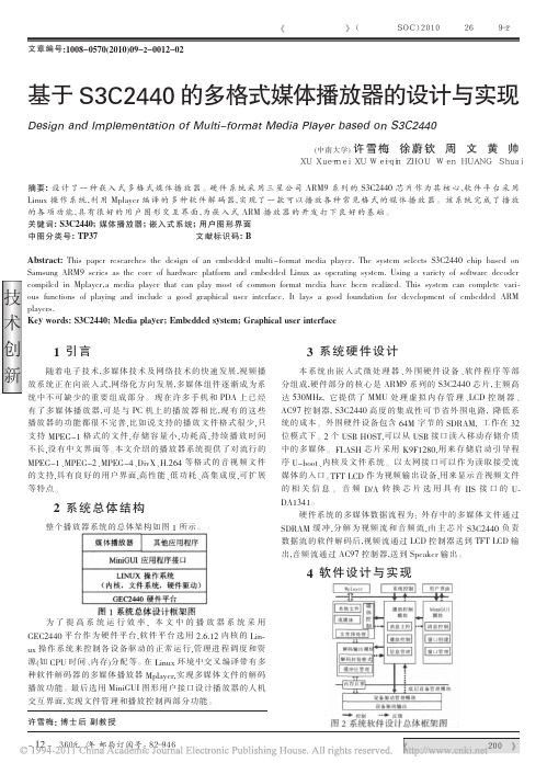
技术创新《微计算机信息》(嵌入式与SOC)2010年第26卷第9-2期博士论坛基于S3C2440的多格式媒体播放器的设计与实现Design and Implementation of Multi-format Media Player based on S3C2440(中南大学)许雪梅徐蔚钦周文黄帅XUXue-meiXUWei-qinZHOUWenHUANGShuai摘要:设计了一种嵌入式多格式媒体播放器。
硬件系统采用三星公司ARM9系列的S3C2440芯片作为其核心,软件平台采用Linux操作系统,利用Mplayer编译的多种软件解码器,实现了一款可以播放各种常见格式的媒体播放器。
该系统完成了播放的各项功能,具有很好的用户图形交互界面,为嵌入式ARM播放器的开发打下良好的基础。
关键词:S3C2440;媒体播放器;嵌入式系统;用户图形界面中图分类号:TP37文献标识码:BAbstract:This paper researches the design of an embedded multi-format media player.The system selects S3C2440chip based on Samsung ARM9series as the core of hardware platform and embedded Linux as operating ing a variety of software decoder compiled in Mplayer,a media player that can play most of common format media have been realized.This system can complete vari-ous functions of playing and include a good graphical user interface.It lays a good foundation for development of embedded ARM players.Key words:S3C2440;Media player;Embedded system;Graphical user interface文章编号:1008-0570(2010)09-2-0012-021引言随着电子技术,多媒体技术及网络技术的快速发展,视频播放系统正在向嵌入式,网络化方向发展,多媒体组件逐渐成为系统中不可缺少的重要组成部分。
Finding community structure in networks using the eigenvectors of matrices
M. E. J. Newman
Department of Physics and Center for the Study of Complex Systems, University of Michigan, Ann Arbor, MI 48109–1040
We consider the problem of detecting communities or modules in networks, groups of vertices with a higher-than-average density of edges connecting them. Previous work indicates that a robust approach to this problem is the maximization of the benefit function known as “modularity” over possible divisions of a network. Here we show that this maximization process can be written in terms of the eigenspectrum of a matrix we call the modularity matrix, which plays a role in community detection similar to that played by the graph Laplacian in graph partitioning calculations. This result leads us to a number of possible algorithms for detecting community structure, as well as several other results, including a spectral measure of bipartite structure in neteasure that identifies those vertices that occupy central positions within the communities to which they belong. The algorithms and measures proposed are illustrated with applications to a variety of real-world complex networks.
可重构计算

可重构计算
可重构计算基于现场可编程门阵列——— FPGA.FPGA的编程技术主要有两种:一种是反 熔丝技术,即通常所说的电可擦写技术,但是这种技 术的可重构实时性太差;另一种是基于静态存储器 ( SRAM)可编程原理的FPGA编程技术,这种硬件 包含计算单元阵列,这些计算单元的功能由可编程 的配置位来决定.当前大多数的可重构设备是基 于静态存储器的,其实现计算单元的粒度随不同的 系统要求而不同.
可重构计算
传统的计算方式有两种: 一种是采用对通用微处理器进行软件编程 的方式,软件的方式通用性好, 但运算速度不 高 一种是采用A S IC 的方式. A S IC 方式处理 速度快, 但只能针对特定的算法, 通用性不 好
可重构计算
可重构计算(Reconfigurable Computing) 是在 软件的控制下, 利用系统中的可重用资源, 根据应 用的需要重新构造一个新的计算平台, 达到接近专 用硬件设计的高性能.具有可重构计算特征的系统 称为可重构系统. 简单地说,就是利用FPGA 逻辑实现计算任 务.有的称作自适应计算(adaptive computing) , 也有的称之为FPGA 计算.
3.独立处理单元模式 独立处理单元模式 属于这类系统的可重构逻辑部分一般包含多个 FPGA .这是一种最松散的耦合形式. 4.SoPC模式 模式 处理器,存储器和可编程逻辑集成在同一个 FPGA 芯片上, 称为单芯片可重构计算系统 (SoPC) .这种系统中CPU 和FPGA仍然是紧密 耦合的结构, 同时片上存储系统和CPU 与FPGA 接口能力则进一步提高了系统的性能.以往的 SoC (System on chip) 设计依赖于固定的ASIC , 而SoPC是以可编程逻辑器件取代ASIC , 越来越 多地成为系统级芯片设计的首选.
天基光学遥感图像的信噪比提升技术综述
航天返回与遥感第 45 卷 第 2 期102SPACECRAFT RECOVERY & REMOTE SENSING2024 年 4 月天基光学遥感图像的信噪比提升技术综述王智 1,2 魏久哲 1,2 王芸 1,2 李强 1,2(1 北京空间机电研究所,北京 100094)(2 先进光学遥感技术北京市重点实验室,北京 100094)摘 要 随着遥感技术的不断发展,天基光学遥感向全时域、智能化方向发展。
微光遥感因需要在夜间和晨昏时段等低照度条件下对地物进行探测,成像具有低对比度、低亮度、低信噪比的特性。
针对低信噪比特性会导致大量复杂物理噪声将图像景物特征淹没,严重影响地面目标识别与判读的情况,文章基于遥感成像的全链路物理模型,总结天基光学遥感图像信噪比提升的技术途径,分别对基于传统滤波的方式、基于物理模型的方式、基于深度学习的方式的研究现状进行分析,对比并总结各类方式中主要代表算法之间的特点及差异,对未来天基光学遥感图像信噪比提升的技术发展方向进行展望。
关键词 去噪算法 全链路模型 信噪比 遥感图像 天基遥感中图分类号:TP751 文献标志码:A 文章编号:1009-8518(2024)02-0102-12DOI:10.3969/j.issn.1009-8518.2024.02.010A Review of SNR Enhancement Techniques forSpace-Based Remote Sensing ImagesWANG Zhi1,2 WEI Jiuzhe1,2 WANG Yun1,2 LI Qiang1,2( 1 Beijing Institute of Space Mechanics & Electricity, Beijing 100094, China )( 2 Key Laboratory of Advanced Optical Remote Sensing Technology of Beijing, Beijing 100094, China )Abstract With the continuous development of the field of remote sensing, space-based remote sensing is developing in the direction of all-sky and intelligent. Since low-light remote sensing is used to detect ground objects under low illumination conditions such as night and morning and night periods, it results in the characteristics of low contrast, low brightness and low signal-to-noise ratio of remote sensing images, among which, low signal-to-noise ratio leads to a large number of complex physical noises drowning the image features, seriously affecting the recognition and interpretation of ground objects. This paper summarizes the actual full-link physical model based on optical remote sensing imaging and the technical approaches to improve the signal-to-noise ratio of remote sensing images, and summarizes the methods based on traditional filtering, physical model and deep learning respectively. By comparing the differences among the main representative algorithms of various methods, the paper summarizes their respective characteristics. The future development direction of the improvement of the signal-to-noise ratio of space-based remote sensing images is forecasted.Keywords denoising algorithm; full link model; SNR; remote sensing image; space-based remote sensing收稿日期:2023-11-03基金项目:国家自然科学基金重点项目(62331006)引用格式:王智, 魏久哲, 王芸, 等. 天基光学遥感图像的信噪比提升技术综述[J]. 航天返回与遥感, 2024, 45(2): 102-113.WANG Zhi, WEI Jiuzhe, WANG Yun, et al. A Review of SNR Enhancement Techniques for Space-Based Remote Sensing Images[J]. Spacecraft Recovery & Remote Sensing, 2024, 45(2): 102-113. (in Chinese)第 2 期王智 等: 天基光学遥感图像的信噪比提升技术综述103 0 引言随着航天技术的迅猛发展,航天遥感技术成为人类认识地球,寻找、利用、开发地球资源,了解全球变化以及气象观测的有效手段。
深度强化学习在自动驾驶中的应用研究(英文中文双语版优质文档)
深度强化学习在自动驾驶中的应用研究(英文中文双语版优质文档)Application Research of Deep Reinforcement Learning in Autonomous DrivingWith the continuous development and progress of artificial intelligence technology, autonomous driving technology has become one of the research hotspots in the field of intelligent transportation. In the research of autonomous driving technology, deep reinforcement learning, as an emerging artificial intelligence technology, is increasingly widely used in the field of autonomous driving. This paper will explore the application research of deep reinforcement learning in autonomous driving.1. Introduction to Deep Reinforcement LearningDeep reinforcement learning is a machine learning method based on reinforcement learning, which enables machines to intelligently acquire knowledge and experience from the external environment, so that they can better complete tasks. The basic framework of deep reinforcement learning is to use the deep learning network to learn the mapping of state and action. Through continuous interaction with the environment, the machine can learn the optimal strategy, thereby realizing the automation of tasks.The application of deep reinforcement learning in the field of automatic driving is to realize the automation of driving decisions through machine learning, so as to realize intelligent driving.2. Application of Deep Reinforcement Learning in Autonomous Driving1. State recognition in autonomous drivingIn autonomous driving, state recognition is a very critical step, which mainly obtains the state information of the environment through sensors and converts it into data that the computer can understand. Traditional state recognition methods are mainly based on rules and feature engineering, but this method not only requires human participation, but also has low accuracy for complex environmental state recognition. Therefore, the state recognition method based on deep learning has gradually become the mainstream method in automatic driving.The deep learning network can perform feature extraction and classification recognition on images and videos collected by sensors through methods such as convolutional neural networks, thereby realizing state recognition for complex environments.2. Decision making in autonomous drivingDecision making in autonomous driving refers to the process of formulating an optimal driving strategy based on the state information acquired by sensors, as well as the goals and constraints of the driving task. In deep reinforcement learning, machines can learn optimal strategies by interacting with the environment, enabling decision making in autonomous driving.The decision-making process of deep reinforcement learning mainly includes two aspects: one is the learning of the state-value function, which is used to evaluate the value of the current state; the other is the learning of the policy function, which is used to select the optimal action. In deep reinforcement learning, the machine can learn the state-value function and policy function through the interaction with the environment, so as to realize the automation of driving decision-making.3. Behavior Planning in Autonomous DrivingBehavior planning in autonomous driving refers to selecting an optimal behavior from all possible behaviors based on the current state information and the goal of the driving task. In deep reinforcement learning, machines can learn optimal strategies for behavior planning in autonomous driving.4. Path Planning in Autonomous DrivingPath planning in autonomous driving refers to selecting the optimal driving path according to the goals and constraints of the driving task. In deep reinforcement learning, machines can learn optimal strategies for path planning in autonomous driving.3. Advantages and challenges of deep reinforcement learning in autonomous driving1. AdvantagesDeep reinforcement learning has the following advantages in autonomous driving:(1) It can automatically complete tasks such as driving decision-making, behavior planning, and path planning, reducing manual participation and improving driving efficiency and safety.(2) The deep learning network can perform feature extraction and classification recognition on the images and videos collected by the sensor, so as to realize the state recognition of complex environments.(3) Deep reinforcement learning can learn the optimal strategy through the interaction with the environment, so as to realize the tasks of decision making, behavior planning and path planning in automatic driving.2. ChallengeDeep reinforcement learning also presents some challenges in autonomous driving:(1) Insufficient data: Deep reinforcement learning requires a large amount of data for training, but in the field of autonomous driving, it is very difficult to obtain large-scale driving data.(2) Safety: The safety of autonomous driving technology is an important issue, because once an accident occurs, its consequences will be unpredictable. Therefore, the use of deep reinforcement learning in autonomous driving requires very strict safety safeguards.(3) Interpretation performance: Deep reinforcement learning requires a lot of computing resources and time for training and optimization. Therefore, in practical applications, the problems of computing performance and time cost need to be considered.(4) Interpretability: Deep reinforcement learning models are usually black-box models, and their decision-making process is difficult to understand and explain, which will have a negative impact on the reliability and safety of autonomous driving systems. Therefore, how to improve the interpretability of deep reinforcement learning models is an important research direction.(5) Generalization ability: In the field of autonomous driving, vehicles are faced with various environments and situations. Therefore, the deep reinforcement learning model needs to have a strong generalization ability in order to be able to accurately and Safe decision-making and planning.In summary, deep reinforcement learning has great application potential in autonomous driving, but challenges such as data scarcity, safety, interpretability, computational performance, and generalization capabilities need to be addressed. Future research should address these issues and promote the development and application of deep reinforcement learning in the field of autonomous driving.深度强化学习在自动驾驶中的应用研究随着人工智能技术的不断发展和进步,自动驾驶技术已经成为了当前智能交通领域中的研究热点之一。
可重构计算
当前可重构计算或系统需要解决的问题
(1) 粒度问题.细粒度的可重构电路面积的使用 效率很低. (2) 如何改进结构来减少重构时间.在数据重载 时,FPGA端口对外呈高阻状态,重载后,才恢复对 外的逻辑功能.这就是所谓的重构时隙,将影响 系统功能的连续.如何克服或减少重构时隙,是 实现动态重构系统的瓶颈问题. (3) 数据传输和存储问题.现在的可重构芯片提 供的片上存储器太少,因而,许多重构计算的应用 需要更大的外部存储器.当前设计中,最迫切需 要优化解决的问题是Memory带宽和能耗.
可重构计算
可重构计算基于现场可编程门阵列——— FPGA.FPGA的编程技术主要有两种:一种是反 熔丝技术,即通常所说的电可擦写技术,但是这种技 术的可重构实时性太差;另一种是基于静态存储器 ( SRAM)可编程原理的FPGA编程技术,这种硬件 包含计算单元阵列,这些计算单元的功能由可编程 的配置位来决定.当前大多数的可重构设备是基 于静态存储器的,其实现计算单元的粒度随不同的 系统要求而不同.
可重构计算的分类
可重构计算又可按重构发生的时间分为静态重构 和动态重构. 静态重构是指在可重构件运行之前对其进行预先 配置, 在运行过程中其功能保持不变, 即运行过程 中不能对其进行重构. 动态重构是指在可可重构件运行的过程中可根据 需要对其实时进行配置, 改变其电路结构, 实现不 同的功能.
可重构计算系统的分类
Garp 是加州大学伯克利分校提出的一种可重构体系结构, 其 结构如图2 所示. 该结构中, 可重构阵列与一个通用的MIPS 处理器构成了一个混合式计算系统, 可重构阵列与通用处理 器共享内存和数据缓冲, 二者之间形成一种主协处理器的关 系. 该结构的优点是兼具了通用处理器的灵活性和可重构部 件的高速性. 通用处理器完成通用程序的处理, 对于特定的 循环和子程序, 则由可重构阵列在通用处理器的控制下实现 加速处理. Garp 结构一般集成在一个芯片上, 形成一个片上 系统.
- 1、下载文档前请自行甄别文档内容的完整性,平台不提供额外的编辑、内容补充、找答案等附加服务。
- 2、"仅部分预览"的文档,不可在线预览部分如存在完整性等问题,可反馈申请退款(可完整预览的文档不适用该条件!)。
- 3、如文档侵犯您的权益,请联系客服反馈,我们会尽快为您处理(人工客服工作时间:9:00-18:30)。
Reconfigurable Computing for Space-Time Adaptive ProcessingNikhil D. Gupta , John K. Antonio , and Jack M. WestDepartment of Computer ScienceBox 43104Texas Tech University Lubbock, TX 79409-3104 USATel: 806-742-1659{gupta, antonio, west}@1. IntroductionSpace-time adaptive processing (STAP) refers to a class of signal processing techniques used to process returns of an antenna array radar system [4]. STAP algorithms are designed to extract desired target signals from returns comprised of Doppler shifts,ground clutter, and jamming interference. STAP simultaneously and adaptively combines the signals received on multiple elements of an antenna array – the spatial domain – and from multiple pulse repetition periods – the temporal domain.The output of STAP is a weighted sum of multiple returns,where the weights for each return in the sum are calculated adaptively and in real-time. The most computationally intensive portion of most STAP approaches is the calculation of the adaptive weight values. Calculation of the weights involves solving a set of linear equations based on an estimate of the covariance matrix associated with the radar return data.Existing approaches for STAP typically rely on the use of multiple digital signal processors (DSPs) or general-purpose processors (GPPs) to calculate the adaptive weights. These approaches are often based on solving multiple sets of linear equations and require the calculation of numerous vector inner products. This paper proposes the use of FPGAs as vector co-processors capable of performing inner product calculation.Two different “inner-product co-processor” designs are introduced for use with the host DSP or GPP. The first has a multiply-and-accumulate structure, and the second uses a reduction-style tree structure having two multipliers and an adder.2.STAP Weight Calculation2.1 Basic FormulationThe STAP algorithm assumed here is known as K th -order Doppler factored STAP, which is classified as a partially adaptive technique. Due to the space limitation, it will not be possible to fully explain this algorithm. Instead, the focus here will be on the necessary notation and core calculations required to determine the values of the adaptive weights. For more information on STAP,the reader is referred to [1, 4].Determining the values for the n -vector of adaptive weights,denoted by w r, involves solving a system of linear equations of the form:s w v r =Ψ,(1)This work was supported by DARPA under contract number F30602-97-2-0297where s ris a known n -vector called the steering vector and Ψis an estimate of the covariance matrix, which is determined based on the sampled radar returns.Ψis derived based on space-time data matrix X , which is an n × N matrix defined by:[]N x x x X rr r ... 21=. Based on this the definition,Ψis given by:H X X N1=Ψ (2)2.2 QR-Decomposition and Conjugate GradientThe QR-decomposition approach is a direct approach for solving a system of linear equations. The QR approach always gives an exact solution and the complexity of the algorithm is fixed. It involves performing a QR-decomposition on the matrix X T , the result of which is an N N ×orthogonal matrix Q and an N n ×upper triangular matrix R such that X = QR . The final result is obtained by forward and backward substitution. For more details the reader is referred to [1].The conjugate gradient approach is an iterative method that provides a general means for solving a system of linear equations [2]. For the system of equations given in Eq. (1), it is based on the idea of minimizing the following function:w s w w w f T r r r r −Ψ=21)(.(3)The function f is minimized when its gradient is zero, i.e.,0=−Ψ=∇s w f rr , which corresponds to the solution to the original system of linear equations. The very repetitive and regular numerical structure of the conjugate gradient update equations makes it a prime candidate for implementation on an FPGA system.Numerical studies were conducted using Matlab implementations of the QR-decomposition and CG methods on actual STAP data collected by the Multi-Channel Airborne Radar Measurement (MCARM) system of Rome Lab [3].Further details of this study can be found in [6].3. Inner-Product FPGA Co-ProcessorEach of the two methods outlined above requires calculating a number of inner products. Given enough resources, all the inner products could be done in parallel on FPGAs. Because the available system has only two FPGAs [5],the computations was divided among the host processor and the FPGA board. The two schemes that were implemented are outlined below. For both schemes, the data vectors are assumed to be in block-floating-point format [9]. Additionally, themultiplier implementation is based on discussion in [7] and the adder unit uses 4-bit carry-look-ahead adders [8] in each stage of the adder pipe.3.1 Multiply-and-Accumulate ImplementationIn the first implementation shown in Figure 1, the FPGA is configured to perform the multiply-and-accumulate operations on the input vectors. The implementation consists of a multiply unit and an accumulator, which is composed of a normalization unit and an adder. The normalization unit shifts the binary point of theprior to the addition. The output of the adder is fed back and accumulated with the next product term.The single cycle multiply-and-accumulate is achieved by pipelining each unit of the implementation. This unit reads in two operands and performs two operations per cycle. Thus, the unit reduces two N -vectors to a constant number of partial sums equal to the number of stages in the accumulator pipe. The implementation allocates approximately 88% of the configurable logic blocks (CLBs) on the Xilinx 4028EX FPGA. The implementation can be clocked at 40MHz, thus giving a throughput of 80 million block-floating-point operations per second.3.2 Multiply-and-Add ImplementationFigure 2 illustrates the second implementation that performs an inner product, i.e., a multiply-and-add operation on the two input vectors. The design incorporates two 16-bit multiply units and an adder. By using this approach, two multiplies can be performed in parallel, and afterwards, the adder computes the sum of the two products.A challenge associated with this implementation is that four 16-bit input operands, i.e., 64 bits, are required per computation cycle. Unfortunately, the data-path to the FPGA board is only 36-bits wide. The solution to this problem involves clocking the input state machine at twice the frequency of the multiply-and-add state machine, and registering the first two operands for one input state machine clock cycle.The multiply-and-add unit reads in four operands and performs three block-floating-point operations per cycle. Thus,the two input N -vectors are reduced to an N /2-vector of partial sums. This implementation, however, involves an additional N /2 addition operations to obtain the inner product result. For this implementation, approximately 99% of the available CLBs on the Xilinx 4028EX FPGA are required. In summary, for a fixed clock rate, the second design can provide a higher throughput, but requires more computation from the host (to perform the final summation of the partial sums).4. References[1]K. C. Cain, J. A. Torres, and R. T. Williams, “Real-TimeSpace-Time Adaptive Processing Benchmark ”, Mitre TR:MTR 96B0000021, Mitre, Bedford, MA, February 1997.[2] D. G. Luenberger, Linear and Nonlinear Programming ,Second Edition, Addison-Wesley, Reading, MA, 1984.[3]Real-Time MCARM Data Sets, .[4] J. Ward, Space-Time Adaptive Processing for AirborneRadar , Technical Report 1015, Massachusetts Institute of Technology, Lincoln Laboratory, Lexington, MA, 1994.[5]Wild-One Hardware Reference Manual 11927-0000Revision 0.1, Annapolis Micro Systems Inc., MD, 1997.[6]Nikhil D. Gupta, Reconfigurable Computing for Space-Time Adaptive Processing , MS Thesis Proposal, TTU,/darpa/reconfigurable/, 1997.[7] T.T. Do, H.Kropp, P. Pirsch, “Implementation of PipelinedMultipliers on Xilinx FPGAs,” Proceedings of the 7th International Workshop on Field-Programmable Logic and Applications , Springer Verlag, September1997[8] M. Morris Mano, Digital Logic and Computer Design ,Second Edition, Prentice Hall, Englewood Cliffs, NJ, 1992[9]W. W. Smith, J. M. Smith , Handbook of Real-Time FastFourier Transforms , IEEE Press, New York, NY, 1995add unit on WildOne FPGA board.。