e2v推出市场领先产品ELiiXA+线阵扫描彩色相机
微视图像产品介绍

单击此处编辑母版标题样式单击此处编辑微视产品在机器视觉领域的介绍及应用北京微视新纪元科技有限公司单击此处编辑母版标题样式 单击此处编辑MV 四目转换盒--MVCL-GEST4特点特点::·简化采集设备·支持远距离传输·PoCL 与CL 兼容·支持相机的类型广泛·配有专用的高帧率配有专用的高帧率,,小体积小体积,,且带自动增益及自动曝光功能的前端相机曝光功能的前端相机,,可配套使用·同步性能同步性能((可扩展可扩展,,转换盒间能够级联转换盒间能够级联))功能功能::可同时支持最多四路CameraLink 相机输入相机输入,,并将采集到的图像数据使用一路千兆网传输给采集系统单击此处编辑母版标题样式 单击此处编辑MV 四目转换盒--MVCL-GEST4应用应用::·立体成像立体成像系统往往需要多路相机同步工作,数据全部传输到采集系统后数据全部传输到采集系统后,,软件根据平面图像合成立体图像面图像合成立体图像。
在此领域在此领域,,工作难点是如何确保采集和识别图像的同步性如何确保采集和识别图像的同步性;;采用MV四目转换盒四目转换盒,,即可以简化采集设备即可以简化采集设备,,又能确保图像的同步性图像的同步性。
·多相机采集系统相机密集的采集系统中可以采用此四目转换盒换盒,,简化采集设备简化采集设备,,提高采集的效率提高采集的效率。
单击此处编辑母版标题样式 单击此处编辑Vision HAWK 智能相机Vision HAWK: 简介:•集成AutoVISION 软件•经过行业验证的机器视觉工具•全方位集成了处理器全方位集成了处理器、、镜头和光源•液体镜头自动对焦•集成以太网网络AutoVISION 软件: 提供简易设置和运行时间界面界面,,可解决基本和中级视觉应用需求可解决基本和中级视觉应用需求。
Visionscape 软件软件((可选可选)): 可使用脚本和其他高级编程功能他高级编程功能。
E2V电子倍增CCD,型号CCD201-20,shouce

CCD201-20Back Illuminated 2-Phase IMO SeriesElectron Multiplying CCD SensorINTRODUCTIONThe CCD201is a large format sensor (41k 2)in the L3Vision TMrange of products from e2v technologies.This device uses a novel output amplifier circuit that is capable of operating at an equivalent output noise of less than one electron at pixel rates of over 15MHz.This makes the sensor well suited for scientific imaging where the illumination is limited.The sensor is a frame transfer device and can operate in inverted mode to suppress dark current as this is now the dominant noise source (even at high readout rate).The image and store sections are designed to operate in 2-phase mode,to maximise the highest achievable parallel transfer frequency.The sensor functions by converting photons to charge in the image area during the integration time period,then transferring this charge through the image and store sections into the readout register.Following transfer through the readout register,the charge is multiplied in the gain register before conversion to a voltage by an output amplifier.The sensor has two output amplifiers;a low noise,high responsivity output for normal CCD operation and a large signal amplifier for when multiplication gain is employed.Operation of the high gain mode is controlled by adjustment of the multiplication phase amplitude R 12HV.GENERAL DATAActive image area .........13.3x 13.3mm Image section active pixels .....1024(H)x 1024(V)Image pixel size ............13x 13m m Number of output amplifiers ..........2Fill factor ...............100%Additional dark reference columns .......32Additional overscan rows ..... (8)PACKAGE DETAILS (see Fig.15)Ceramic PackageOverall dimensions .........37.4x 26.5mm Number of pins ..............36Inter-pin spacing ........... 2.54mm Mounting position .............anyThe pin 1marker isshown in Fig.15.STORAGE AND OPERATION TEMPERATURE EXTREMESMINMAX Storage temperature (8C)7200+100Operating temperature (8C)7120+75Temperature ramping (8C/min)–5Note:Operation or storage in humid conditions may give rise to moisture on the sensor surface on cooling,causing irreversible damage.#e2v technologies (uk)limited 2005A1A-100013Issue 1,June 2005411/9140e2v technologies (uk)limited,Waterhouse Lane,Chelmsford,Essex CM12QU,UK Telephone:+44(0)1245493493Facsimile:+44(0)1245492492e-mail:enquiries@ Internet: Holding Company:e2v technologies plc e2v technologies inc.4Westchester Plaza,PO Box 1482,Elmsford,NY10523-1482USA Telephone:(914)592-6050Facsimile:(914)592-5148e-mail:enquiries@TYPICAL PERFORMANCE SPECIFICATIONSExcept where otherwise specified,the following are measured for operation at a pixel rate of15MHz,with typical operating voltages. Parameters are given at223K unless specified otherwise.Where parameters are different in the normal and high gain mode,both are given.PARAMETER UNIT MIN TYPICAL MAX Output amplifier responsivity,HR amplifier(normal mode)(see note1)m V/e7– 5.3–Output amplifier responsivity,LS amplifier(normal mode)(see note1)m V/e7– 1.4–1–1000 Multiplication register gain,LS amplifier(high gain mode)(see notes2,3and4)Peak signal-2-phase IMO e7/pixel50k80k–Charge handling capacity of multiplication register(see note5)e7/pixel–730k–Charge handling capacity of HR amplifier(see note6)e7–280k–Charge handling capacity of LS amplifier(see note6)e7–1M–e7rms– 3.1–Readout noise at50kHz with CDS,HR amplifier(normal mode)(see note6)e7rms– 6.0–Readout noise at1MHz with CDS,HR amplifier(normal mode)(see note6)e7rms–50–Amplifier reset noise(without CDS),HR amplifier(normal mode)(see note6)Readout noise at15MHz with CDS,LS amplifier(normal mode)e7rms–43–(see note6)Amplifier reset noise(without CDS),LS amplifier(normal mode)e7rms–100–(see note6)Readout noise at1MHz(high gain mode)(see note6)e7rms–51–Maximum frequency(settling to1%),HR amplifier(see notes6and7)MHz––3 Maximum frequency(settling to5%),HR amplifier(see notes6and7)MHz–– 4.5 Maximum frequency(settling to1%),LS amplifier(see note6and7)MHz––13 Maximum frequency(settling to5%),LS amplifier(see note6and7)MHz––20 Maximum parallel transfer frequency(see note1)MHz–0.9–Dark signal at293K(see note8)e7/pixel/s–260530 Dark signal non-uniformity(DSNU)at293K(see note9)e7/pixel/s–90–Excess noise factor(see note10)–H2–NOTES1.Measured at a pixel rate of1MHz.2.The typical variation of gain with R12HV is shown in Fig.1.3.The variation of gain with R12HV at different temperatures is shown in Fig.1.4.Some increase of R12HV may be required throughout life to maintain gain performance.Adjustment of R12HV should belimited to the maximum specified under Operating Conditions.5.When multiplication gain is used and clock timings optimised,a linear response of output signal with input signal of better than3%is achieved for output signals up to400ke7typically.6.These values are inferred by design and not measured.7.The quoted maximum frequencies assume a20pF load and that correlated double sampling is being implemented.8.The quoted dark signal has the usual temperature dependence for inverted mode operation.For operation at high frame rateswith short integration times,there will also be a component generated during readout through the register.Operating at a temperature of293K and10Hz frame rate,the readout component contributes5.8e7/pixel/frame typically,at a gain of1000 and referenced to the image area,and has a temperature dependence consistent with non-inverted mode operation.There exists a further weakly temperature dependent component,the clock induced charge,which is independent of the integration time.The clock induced charge is dependent on the operating biases and timings employed and is typically0.2e7/ pixel/frame at T=7558C.For more information,refer to the technical note"Dark Signal and Clock-Induced Charge in L3Vision TM CCD Sensors".9.DSNU is defined as the1s variation of the dark signal.10.The excess noise factor is defined as the factor by which the multiplication process increases the shot noise on the image whenmultiplication gain is used.100013,page2#e2v technologiesDEVICE COSMETIC PERFORMANCEGrade1devices are supplied to the blemish specification shown below.Note that incorrect biasing of the device may result in spurious dark or white blemishes appearing.These will be eliminated if the biases are adjusted.Test ConditionsOperating mode Devices run in2-phase inverted mode,with an integration time of100ms and a readout rate of15MHz.Sensor temperature18+38C.Multiplication gain Set to approximately1000.Illumination Set to give a signal level of approximately60e7/pixel/frame.BLEMISH SPECIFICATIONBlack Columns Black defects are counted when they have a responsivity of less than80%of the local mean signalat approximately the specified multiplication gain and level of illumination.A black column containsat least9contiguous black defects.White Columns White defects are pixels having a dark signal generation rate corresponding to an output signal ofgreater than5times the maximum specified dark signal level.A white column contains at least9contiguous white defects.Pin-Head Columns Pin-head columns are manifest as a partial dark column with a bright pixel showing photoresponseat the end of the column nearest to the readout register.Pin-head columns are counted when theblack column has a responsivity of less than80%of the local mean signal at approximately thespecified multiplication gain and level of illumination.A pin-head column contains at least9contiguous black defects.SPECIFICATIONPARAMETER GRADE1SPECIFICATION GRADE2SPECIFICATIONWhite Columns00Black/Pin-head Columns16ORDERING INFORMATIONPART NUMBER OPERATING MODE COATING WINDOWCCD201-20-*-1222-phase Midband Temporary*denotes grade of device.#e2v technologies100013,page31000100101R 12HV (V)M U L T I P L I C A T I O N G A I NFigure 1:TYPICAL VARIATION OF MULTIPLICATION GAIN WITH R 12HV AT DIFFERENT TEMPERATURESFigure 2:TYPICAL VARIATION OF DARK SIGNAL WITH TEMPERATURE100013,page 4#e2v technologies10711072110102103104D A R K S I G N A L (e 7/p i x e l /s )SENSOR TEMPERATURE (8C)74072002040829910090807060504030201003004005006007008009001000WAVELENGTH (nm)Q U A N T U M E F F I C I E N C Y (%)8216Figure 3:TYPICAL SPECTRAL RESPONSE (At 7208C,no window,midband coating)#e2v technologies 100013,page 5ESD HANDLING PROCEDURESCCD sensors,in common with most high performance IC devices,are static sensitive.In certain cases a static electricity discharge may destroy or irreversibly degrade the device.Accordingly,full anti-static handling precautions should be taken whenever using a CCD sensor or module.These include:*Working at a fully grounded workbench.*Operator wearing a grounded wrist strap.*All receiving socket pins to be positively grounded.*Unattended CCDs should not be left out of their conducting foam or socket.All devices are provided with internal protection circuits to most gate electrodes but not to the other pins.Evidence of incorrect handling will terminate the warranty.EXPOSURE TO RADIATIONExposure to radiation may irreversibly damage the device and result in degradation of ers wishing to operate the device in a radiation environment are advised to consult e2v technologies.ABSOLUTE MAXIMUM RATINGSMaximum ratings are with respect to SS.PIN CONNECTION DESCRIPTION MIN(V)MAX(V)1ABD Anti-blooming Drain(see note11)70.3+252SS Substrate03I14Image Clock4720+204I13Image Clock3720+205S14Store Clock4720+206S12Store Clock2720+207SS Substrate08SS Substrate09DG Dump Gate720+2010OG Output Gate720+2011ODH Output Drain(HR Amplifier)70.3+3212RD Reset Drain70.3+2513ODL Output Drain(LS Amplifier)70.3+3214SS Substrate015OSH Output Source(HR Amplifier)(see note12)70.3+2516OSL Output Source(LS Amplifier)(see note12)70.3+25171R Reset Pulse720+2018R1DC Multiplication Register DC Bias720+2019R12HV Multiplication Register Clock720+5020DG Dump Gate720+2021n.c.Not Connected22n.c.Not Connected23SS Substrate024n.c.Not Connected25n.c.Not Connected26DD Dump Drain70.3+2527R13Register Clock3720+2028R11Register Clock1720+2029R12Register Clock2720+2030SS Substrate031S13Store Clock3720+2032S11Store Clock1720+2033I11Image Clock1720+2034I12Image Clock2720+2035SS Substrate036IG Isolation Gate720+20NOTES11.Anti-blooming is not available on this device type.However,ABD is used for connection purposes and must be biased asspecified.12.Permanent damage may result if,in operation,OSL or OSH experience short-circuit conditions.100013,page6#e2v technologiesOPERATING CONDITIONSTypical operating voltages are as given in the table below.Some adjustment within the minimum-maximum range specified may be required to optimise performance.CONNECTION PULSE AMPLITUDE OR DC LEVEL (V)MinTypical MaxI 11,2,3,4high +5(see note 13)+7+9(see note 13)I 11,2,3,4low 767574S 11,2,3,4high +5(see note 13)+7+9(see note 13)S 11,2,3,4low 767574R 11,2,3high +8+12+13R 11,2,3low –0–R 12HV high +20+40+50(see note 4)R 12HV low 0+4+51R high see note 14+10see note 141R low –0–R 1DC +2+3+5OG +1+3+5IG –75–SS 0+4.5+7ODL,ODH +25+28+32RD +15+17+20ABD +10+18+20DG low –0–DG high +10+12+13DD+20+24+25NOTES13.I 1and S 1adjustment may be common.14.1R high level may be adjusted in common with R 11,2,3.15.Between the two amplifiers,common connections are made to the reset gates (1R),reset drains (RD)and output gates (OG).16.An external load is required for each output amplifier.For the HR amplifier,this can be a resistor of about 5k O (non-critical)or aconstant current type of about 5mA.For the LS amplifier,the load should be either 3.3k O or 7.5mA.The on-chip amplifier power dissipation is approximately 30mW for the HR amplifier and 50mW for the LS amplifier.#e2v technologies 100013,page 7Maximum voltages between pairs of pins:PIN CONNECTION PIN CONNECTION MIN(V)MAX (V)15OSH 11ODH 715+1516OSL 13ODL 715+1519R 12HV 18R 1DC 720+5019R 12HV27R 13720+50Output transistor current (mA)20DRIVE PULSE WAVEFORM SPECIFICATIONThe device is of a4-phase construction,designed to operate in2-phase inverted mode.This is achieved by applying common timings to phases11and12,and phases13and14of the image and store sections.Suggested timing diagrams are shown in Figs.4–11. The following are suggested pulse rise and fall times.CLOCK PULSE TYPICAL RISE TIME t(ns)TYPICAL FALL TIME t(ns)TYPICAL PULSE OVERLAPI11405t52001405t5200@90%pointsS11405t52001405t5200@90%pointsR111010@70%pointsR121010@70%pointsR131010@70%pointsR12HV2525see note18R12HV Sine Sine Sinusoid-high on falling edge of R11NOTES17.Register clock pulses are as shown in Figs.5and6.18.An example clocking scheme is shown in Fig.5.R12HV can also be operated with a normal clock pulse,as shown in Fig.6.Therequirement for successful clocking is that R12HV reaches its maximum amplitude before R11goes low. ELECTRICAL INTERFACE CHARACTERISTICSELECTRODE CAPACITANCES AT MID CLOCK LEVELSConnection Capacitance to SS Inter-phase Capacitances Total Capacitance UnitsI11 2.4 2.47.2nFI12 5.4 2.410.2nFI13 2.4 2.47.2nFI14 5.4 2.410.2nFS11 2.4 2.47.2nFS12 5.4 2.410.2nFS13 2.4 2.47.2nFS14 5.4 2.410.2nFR116898166pFR125668124pFR138974163pFR12HV151833pF SERIES RESISTANCESConnection Approximate Total Series ResistanceI1116OI1214OI1316OI1414OS1116OS1214OS1316OS1414OR116OR126OR136OR12HV8O APPROXIMATE OUTPUT IMPEDANCELarge Signal Amplifier350OHigh Responsivity Amplifier400O 100013,page8#e2v technologies11 12 13 148184APULSE TIMINGS AND OVERLAPSFigure4:CLOCKING SCHEME FOR2-PHASE INVERTED MODE OPERATION#e2v technologies100013,page9R 12HVR 11R 12R 138237Figure 5:CLOCKING SCHEME FOR MULTIPLICATION GAIN(Sine wave clocking scheme)(see note 19)Figure 6:CLOCKING SCHEME FOR MULTIPLICATION GAIN(Conventional clocking scheme)(see note 19)NOTE19.To operate through the OSH output amplifier,the R 11and R 12waveforms should be interchanged.100013,page 10#e2v technologiesR 12HVR 11R 12R 138238Figure 7:RESET PULSET W =10ns typical T 1=output valid T 240nsFigure 8:PULSE AND OUTPUT TIMING#e2v technologies 100013,page11VOS8069I 11=I 12I 13=I 14S 11=S 12S 13=S 14R 11R 12R 13R 12HV1RExtended first pulse at typ.8280Figure 9:EXAMPLE FRAME TIMING DIAGRAMFigure 10:EXAMPLE LINE TIMING DIAGRAM (Operation through OSL,see notes 19and 22)100013,page 12#e2vtechnologiesI 11=I 12I 13=I 14S 11=S 12S 13=S 14R 11R 12R 13R 12HVR 11R 12R 13DGS 11S 12S 13S 148187Figure 11:OPERATION OF THE DUMP GATE TO DUMP n LINES OF UNWANTED DATA FROM THE STANDARD REGISTERNOTE20.Wanted lines of data must be completely read out before dumping unwanted data.Figure 12:OUTPUT CIRCUIT SCHEMATIC (OSL and OSH Amplifiers)NOTE21.The amplifiers have a DC restoration circuit that is internally activated whenever S 14is high.#e2v technologies 100013,page 1312345678910111213142324252627282930313233343536ABD SS I 14I 13S 14S 12SS SS DGOG ODH RD ODL SS SSDD R 13R 11R 12SS S 13S 11I 11I 12SS IG 16168297Figure 13:SCHEMATIC CHIP DIAGRAMFigure 14:LINE OUTPUT FORMAT (for Example Line Timing Figure 10)NOTE22.There is a 1-line propagation delay between transferring a line from the store section to the standard register and reading it outthrough the OSL output amplifier.100013,page 14#e2v technologies16OVERSCAN15DARK REFERENCE1024ACTIVE OUTPUTS15DARK REFERENCE8283***=Partially shielded transition elementsPIN Figure 15:PACKAGE OUTLINEOutline NoteThe image centre is aligned centrally in the package in direction ‘X’,to within a tolerance of +0.2mm.G 0.46+0.05H 22.86+0.23J 33.02+0.33K2.54+0.13Printed in England #e2v technologies 100013,page 15Whilst e2v technologies has taken care to ensure the accuracy of the information contained herein it accepts no responsibility for the consequences of any use thereof and also reserves the right to change the specification of goods without notice.e2v technologies accepts no liability beyond that set out in its standard conditions of sale in respect of infringement of third party patents arising from the use of tubes or other devices in accordance with information contained herein.。
德国Super_DolinaⅡ型、Welta和WITTNAUER三款自动测距高档135相机

相机世界德国Super Dolina Ⅱ型、Welta和WITTNAUER图文|雨晨倩当下,相机收藏已进入到向深度、广度和高质量发展的新阶段。
新、老、名、特相机已成为相机收藏爱好者淘机的主要目标和相机收藏研究的佳品。
除此之外,伴随老相机的收藏,有关老镜头和摄影老物件、特别是老照片的收藏已提上了日程,老相机和老照片的收藏相辅相成,密切相关。
实际上,有关国内老照片的收藏情况过去已有较多的报道。
一些有识之士早已开始了老照片的收藏和系统的研究,而且卓有成效、成绩斐然。
现如今,早期的原版老照片已日益减少、难以淘到而且价格不菲。
但是有关老照片的画册、书刊等的出版物还比较丰富,同样也可以用来收藏、研究和欣赏。
经常翻阅这些画册、出版物可以看到这些老照片不仅具有重要的历史史料价值,而且还展现出深厚的文化内涵。
通过照片的今昔对比,不但可以看到城乡面貌的巨大变化,而且也能看到社会制度和人文景观演变的清晰过程。
因此,老照片的收藏和研究,不仅有助于老相机收藏水平的提高,还能从中得到许多有益的启示。
在一些有关老照片的出版物中,有一本书名为《外国人拍摄的中国影像1844-1949》很值得一看(图1)。
该书由中国国家博物馆历史老照片资深研究员编写,书中图文并茂系统地介绍了早期的外国摄影师在我国拍摄的老照片的活动过程。
这本书对于研究了解世界照相机的发展历史和这些老照片的历史价值有所帮助。
除此之外,在另一本老照片的丛书中(图2)还谈到了使用柯达公司生产的6英寸沙克梯360°全景相机拍摄的团体照片的经过,并附有一张1米多长的历史老照片。
这本老照片丛书由山东画报社编写,1996年第一次印刷,图文并茂,计划每年出版四至五辑。
这张长卷老照片刊登在老照片的第三辑上,文章名为“展长卷,忆昔年”。
图3为团体合影的老照片(由于纸张和印刷质量不佳,照片不是很清晰,用放大镜观看效果好一些)。
照片的上面写着“北平私立汇文学校全体师生合影”。
这张照片拍摄于1946年5月5日,照片长4.2英尺,宽6英寸,长度有1米多。
深耕机器视觉,Teledyne e2v全局快门图像传感器显威力

图像传感器12ELECTRONIC ENGINEERING & PRODUCT WORLD 2021.4深耕机器视觉,Teledyne e2v全局快门图像传感器显威力张耀强 (Teledyne e2v专业成像部门副总裁)1 机器视觉行业的全局快门图像传感器机会Teledyne e2v 是Teledyne Technologies 旗下公司,也是全球领先的高性能图像解决方案供应商。
Teledyne e2v 针对机器视觉市场提供高性能图像传感器、定制化的摄像头解决方案以及特定应用的标准产品。
公司研发的全局快门图像传感器,由于其成像质量好、噪声低、帧率高,并且集成了相应的处理功能,受到了客户的广泛欢迎。
现在我们的产品应用于工业相机、智能扫码、人脸识别、智能交通系统和工业人工智能等领域,统称为机器视觉领域。
在工业领域,机器视觉被广泛用于自动检验、工件加工、装配自动化以及生产过程控制和监视图像识别。
对产品质量需求的提升,促进了机器视觉在汽车、电子、半导体、食品和包装行业的发展。
事实上,机器视觉已经“飞跃”工厂,现身于农场、道路和停车场(如车牌识别)、物流仓储等多种环境。
据统计,全球机器视觉相机市场将从2020年的36亿美元增长到2026年的55亿美元左右,复合年增长率(CAGR )为7.4%。
为了能够更好地抓住机器视觉行业爆发增长的历史机遇,我们深耕每个行业,了解客户的需要和痛点,推出了很多产品,并集成了相应功能帮助客户降低使用门槛和增加使用便利性。
2 工业图像传感器的发展动向工业4.0的首要目的是在解放劳动力的前提下实现生产力与生产质量的进一步提高。
我们认为,核心竞争力比的是 “快速”和“精准”(精准是能力,也是质量)。
智能制造的核心是“智”。
“智”的核心就是信息获取的快和准,信息处理的快和准。
一个人的武功高低,要看“手眼身法步”,要想成为智能制造的武林高手,“眼力”和“招法”的水准是核心之中的核心。
Rolleiflex_2.8F_双反相机里的极品佼佼者

Rolleiflex 2.8FRolleiflex2.8 F 2443187【维吾尔族儿童】黑白负片,2014年10月禄来双反相机在中画幅的各类双反相机中,操作便捷,测光准确,对焦迅速,在人文题材的拍摄上更有较强的优势。
此外,中画幅的篇幅,可以将人物的表情等细节很好的展现出来。
R ollei是引领双反相机市场的前锋1929年,禄莱推出了6×6cm的中画幅双镜头反光相机,其最大的特点是上镜头取景,下镜头摄影。
期间,无数的品牌争相效仿,但很少有相机能够超越Rolleiflex 。
Rollei双反相机大约生产了20多款机型,外观风格和内部结构上基本没有太大改变。
其中,Rollekonter和Rolleicord是面向普通大众市场的,但它们也具备了相当水准的机械及光学素质。
而Rolleiflex,则直接定位于高端专业类型,追求得是“百年有形”,并按照高级专业水准而设计制造,并相继生产出了E 、F 、T 等几种型号。
这几种相机在机械结构、生产工艺、制造技术、产品配套及性能上均达到了较高技术水平。
在Rollei的6×6cm双反相机中,主要有Rolleiflex 和Rolleicord两个系列,分别刻在相机前面版的顶部。
在Rolleiflex系列里面按最大光圈不同又分为2.8和3.5系列,配合使用的蔡司镜头结构为Tessar和Planar, 施耐德镜头为Xenar和Xenotar。
各型号间在成像风格上,还是有差异的,这主要与所使用的镜头有关系。
如,蔡司Tessar结构的镜头,成像锐利、如同刀刻;Planar 结构的镜头,成像细腻而柔和,层次丰富,过渡自然,影调的再现和空间感有一种特殊的味道;使用施耐德镜头的成像特点则是清晰度高、反差强烈、色彩明快、饱和度高等。
R olleiflex 2.8F依旧百般迷人在Rolleiflex系列里有3.5E、3.5T、3.5F、3.5MX、2.8A、2.8D、2.8B、2.8F等型号。
英国MICROFLEX和MICRCORD两款120双反相机
英国MICROFLEX和MICRCORD 两款120双反相机图文|雨晨倩120双镜头反光相机是职业摄影师和广大摄影爱好者最喜欢使用的机型之一。
自从德国的禄来弗莱克斯120双反相机和徕卡35mm相机成功上市以来,不但对世界照相机的发展产生了重大的影响,而且也使世界照相机发展的格局产生了重要的变化。
昔日广为流行的大画幅相机开始淡出相机市场,而以德国发明的中小画幅相机逐渐成为流行的机种,开启了经典相机时代的新纪元,德国也开始成为中小画幅相机的研制和生产中心。
由于中小画幅所拍摄的底片很小,需要放大成大幅照片以适合观赏,因此中小画幅相机的流行也带动了感光材料、暗房设备、照相馆等的迅速发展。
历史上,一款新机型的发明和成功上市,必然会引起世界许多国家的相机厂的极大关注。
为了在激烈竞争的相机市场占有一席之地,名牌相机的仿制品、改制品和经过重新设计的各种同类型的相机品牌也很快出现在相机市场上,因此,呈现出同一种类型相机多元化的发展趋势,120双反相机就是这一现象最好的例证。
德国的禄来120双反相机外观设计新颖、美观、别具一格,加工制作精密精良、功能完善、使用方便、经久耐用、镜头素质一流,成为相机的主要特点。
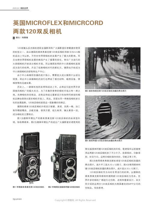
图1为德国早期生产的禄来弗莱克斯120双反相机的标准型外观,俗称黑禄来。
图2为德国早期生产的适合广大摄影爱好者使用的简化版禄来柯德120双反相机的外观。
笔者很早以前曾使用这两款120双反相机拍了不少片子,效果很好,印象深刻。
时至今日,这两台相机保存完好,仍能正常工作。
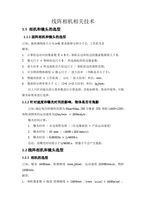
图3为使用禄来弗莱克斯标准型120双反相机拍摄的黑白照片,底片手工放大10×12英寸。
图4为使用禄来柯德120双反相机拍摄的黑白照片,底片放大10×12英寸。
120双反相机作为当时非常流行的机种,以德国的禄来弗莱克斯和禄来柯德两款120双反相机为范本,世界许多的相机厂都进行过仿制、改制和重新设计。
本文所介绍的这两台120双反相机为英国著名的MPP公司的仿制品,仅供参考。
ZEISS Axiocam 512 color 12 Megapixel微观相机说明书

ZEISS Axiocam 512 colorYour 12 Megapixel Microscope Camera for Imagingof Large Sample Areas – Fast, in True Color, and High ResolutionProduct Information Version 1.1Technical Specifications› ServiceTechnical Specifications› ServiceTechnical Specifications› ServiceTechnical Specifications› Technology and Details› ServiceTechnical SpecificationsWave Length (nm)Blue Green Red› Technology and Details › ServiceBecause the ZEISS microscope system is one of your most important tools, we make sure it is always ready to perform. What’s more, we’ll see to it that you are employing all the options that get the best from your microscope. You can choose from a range of service products, each delivered by highly qualified ZEISS specialists who will support you long beyond the purchase of your system. Our aim is to enable you to experience those special moments that inspire your work.Repair. Maintain. Optimize.Attain maximum uptime with your microscope. A ZEISS Protect Service Agreement lets you budget for operating costs, all the while reducing costly downtime and achieving the best results through the improved performance of your system. Choose from service agreements designed to give you a range of options and control levels. We’ll work with you to select the service program that addresses your system needs and usage requirements, in line with your organization’s standard practices.Our service on-demand also brings you distinct advantages. ZEISS service staff will analyze issues at hand and resolve them – whether using remote maintenance software or working on site. Enhance Your Microscope System.Your ZEISS microscope system is designed for a variety of updates: open interfaces allow you to maintain a high technological level at all times. As a result you’ll work more efficiently now, while extending the productive lifetime of your microscope as new update possibilities come on stream.Profit from the optimized performance of your microscope system with services from ZEISS – now and for years to come.Count on Service in the True Sense of the Word>> /microservice› Technology and Details › ServiceN o t f o r t h e r a p e u t i c , t r e a t m e n t o r m e d i c a l d i a g n o s t i c e v i d e n c e . N o t a l l p r o d u c t s a r e a v a i l a b l e i n e v e r y c o u n t r y . C o n t a c t y o u r l o c a l Z E I S S r e p r e s e n t a t i v e f o r m o r e i n f o r m a t i o n .E N _40_011_104 | C Z 09-2016 | D e s i g n , s c o p e o f d e l i v e r y a n d t e c h n i c a l p r o g r e s s s u b j e c t t o c h a n g e w i t h o u t n o t i c e . | © C a r l Z e i s s M i c r o s c o p y G m b HCarl Zeiss Microscopy GmbH 07745 Jena, Germany ********************/axiocam。
线阵相机相关技术
1.2 线阵相机和镜头选型
1.2.1 相机的选型
已知:幅宽 1600mm、检测精度 1
慘 、 ݔ运动速度 22000
、物距
1300 ;
解答:
1. 相机像素数 = 幅宽/检测精度 = 1600 / 1 /pixel = 1600 慘 ݔ,
2. 最少 2000 个像素,选定为 2k 相机; 3. 扫描行频 = 运动速度/实际检测精度 = 22000 /0.
线阵相机相关技术
1.1 相机和镜头的选型
1.1.1 面阵相机和镜头的选型
已知:被检测物体大小为 A*B,要求能够分辨小于 C,工作距为 D 解答: 1. 计算短边对应的像素数 E = B/C,相机长边和短边的像素数都要大于 E; 2. 像元尺寸 = 物体短边尺寸 B / 所选相机的短边像素数; 3. 放大倍率 = 所选相机芯片短边尺寸 / 相机短边的视野范围; 4. 可分辨的物体精度 = 像元尺寸 / 放大倍率 (判断是否小于 C); 5. 物镜的焦距 = 工作距离 / (1+1 / 放大倍率) 单位: ; 6. 像面的分辨率要大于 1 / (2*0.1*放大倍率) 单位:lp ;