ML8511 紫外线传感器 封装很小
哈希紫外可见分光光度计常见的故障及处理方法
哈希紫外可见分光光度计常见的故障及处理方法哈希紫外可见分光光度计直观的菜单导航系统以及彩色触摸屏使客户通过几个简单的步骤即可输入和校准自定义方法;支持定制化应用,可满足对精度要求苛刻的客户需要;内置AQA具有计划,管理和记录功能;支持以太网连接,可以快速的获取数据并进行实时的数据传输。
可广泛应用于工业,市政,环保,教育科研,疾控等领域的实验室水质监测。
故障及解决方法:
1、光源灯不亮
查看光源灯是否损坏,电源是否无电源输出。
更换新的光源灯。
2、哈希光度计光门未打开
检查光门是否活络,是否有异物卡住。
3、接收器无信号输出
检查接收器插头有没有插好,或接触不良;检查接收器是否损坏,如损坏需更换新的接收器。
4、哈希光度计测光不正常
考虑是否样品处理错误,或比色皿不配对。
需正确处理样品,扣除比色皿配对误差后测量。
考虑仪器是否波长误差过大,用镨钕玻璃检查,并调整波长。
5、哈希光度计数值无法输入上层软件
考虑与计算机有关的电路串行通讯故障,考虑输出接口故障。
请与厂商联系维修。
6、哈希光度计出现“Err3”错误
一般是由于操作错误导致,将仪器关机重启可解决。
7、开启电源开关后仪器无反应
故障原因排查:电源未接通;保险丝熔断;机内插件松动等。
解决办法:检查电源插头是否连接良好、电源电缆是否断线;检查保险丝,若保险丝熔断需更换新的保险丝;若插件松动,拔出重新插好。
紫外线传感器 UV sensor ML8511
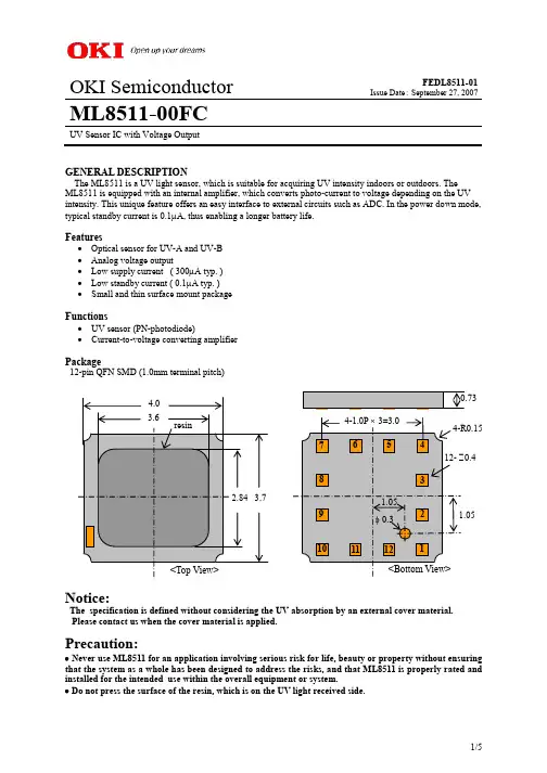
Features
Optical sensor for UV-A and UV-B Analog voltage output Low supply current ( 300A typ. ) Low standby current ( 0.1A typ. ) Small and thin surface mount package
Functions
UV sensor (PN-photodiode) Current-to-voltage converting amplifier
Package
12-pin QFN SMD (1.0mm terminal pitch) 4.0 3.6 0.73 resin 4-1.0P 3=3.0 4-R0.15 4 12- 0.4
RECOMMENDED Βιβλιοθήκη PERATING CONDITIONS
Parameter Operating Voltage Input Voltage(High Level) Input Voltage(Low Level) Operating Temperature Symbol VDD VIH VIL Ta Min. 2.7 2.16 -0.2 0 Typ. 3.3 Max. 3.6 VDD + 0.3 0.72 70 unit V V V C
2/5
FEDL8511-01 OKI Semiconductor ML8511-00FC
ABSOLUTE MAXIMUM RATINGS
Parameter Supply Voltage Input Voltage Output Short Current Power Dissipation Storage Temperature Symbol VDD VI IOS PD Tstg Condition Ta=25 C Ta=25 C Ta=25 C Ta=25 C Rating -0.3 to +4.6 -0.3 to +4.6 5 30 -30 to +85 unit V V mA mW C
ROHM Sensing Solutions ML8511 超声波感应解决方案 IC 应用说明说明书
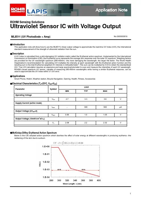
1ROHM Sensing SolutionsUltraviolet Sensor IC with Voltage OutputML8511 (UV Photodiode + Amp)●IntroductionThis application note will show how to use the ML8511’s linear output voltage to approximate the real-time UV Index (UVI), the international standard measurement of the strength of ultraviolet radiation from the sun.●DescriptionA UV Index is calculated from a skin-damaging UV radiation metric called the Erythemal action spectrum. Implemented by the International Commission on Illumination (CIE), the Erythemal curve represents the average skin response over the solar UV spectrum. Weighing factors are provided for the UV wavelength spectrum (280-400nm) –the more damaging the wavelength, the larger the factor. The World Health Organization’s recommendation for calculating UVI multiplies the intensity at each wavelength with the Erythemal action function and the resulting sum is the total Erythemal-weighted UV intensity in milliwatts/meter 2. This sum can be multiplied by 0.04 to obtain the standardized UVI. True UVI calculation requires an expensive and large spectrophotometer to scan and measure the intensities of each UV wavelength. ROHM’s broad spectrum UV sensor, capable of measuring 280-400nm wavelengths while having a similar Erythemal response, can be used to approximate the UV Index within ±1 UVI error.●ApplicationsSmart Phone, Watch, Weather station, Bicycle Navigation, Gaming, Health, Fitness, Accessories●Electrical Characteristics (T a =25°C, V EN =V DD )Parameter SymbolLimitUnitMINTYPMAXOperating VoltageV DD2.73.33.6VSupply Current (active mode)I DDA - 300 500 µAOutput Voltage (UV AB =0)V REF 0.95 1.0 1.05 VOutput Voltage (10mW/cm 2 at λP )V o 2.08 2.2 2.32 V●McKinlay-Diffey Erythemal Action SpectrumBelow is the CIE adopted action spectrum which desribes the effect of solar energy at different wavelengths in producing erythema –the reddening of the skin due to sunburn.No.0000000016●Test Equipment and Measurement ProcedureAn ML8511 evaluation board, powered at 3.3V DD , was used with a multimeter to measure and record analog voltages during variousultraviolet intensities throughout the day. In addition, a National Institute of Standards and Technology (NIST) traceable and calibrated Solarmeter Model 6.5 UVI Meter was used alongside ML8511’s sensor opening to record actual UVI. During testing, both the ML8511 sensor and UVI meter were facing straight up toward a global normal (perpendicular to level ground) inclination. Solar irradiance measured this way includes direct (solar zenith angle) and diffuse (atmospheric diffusion) rays.During the measurement process, the ML8511 sensor was used without a protective lens. ROHM recommends the usage of an optical lens/filter in end product design. Due to the lack of a diffusive transmission lens, solar irradiance is not uniform across the active area of the ML8511. The maximum voltages were typically seen when the sensor was facing the sun while still parallel to the ground and minimum voltages resulted with a 90° rotation. For accurate solar measurements independent of sensor orientation, the maximum and minimum voltages were taken and averaged before the UVI approximation calculation.●Calculation of the actual UV Index from Vout of ML8511Application: ML8511 + Ideal Lens filter (100% transmission of UVA + UVB)*. This section will first describe how to derive ROHM’s UVI approximation equation from the UVI function. UVA and UVB are given a fixed ratio and their respective Erythemal factors are averaged. The resulting equation will approximate the UVI from Vout of ML8511 with an ideal filter with 100% UV transmission characteristics.Key points to remember:1. ML8511 measures the total UV strength of UVA and UVB (un-weighted UV strength)2. Voltage output from ML8511 is directly proportional to the total strength of UVA + UVB3. Under most solar conditions, the ratio of UVA/UVB is a fixed value. UVI can be approximated by multiplying the output of ML8511by a factor.UV Index Function:UVI =(�SS (λ)∗Ery (λ))∗0.04Variables:SS(λ) = Solar Irradiance SpectrumEry (λ) = McKinlay -Diffey Erythemal Action SpectrumAssumed fixed ratio � UV A = UVTotal ∗ 94.1%UVB = UVTotal ∗ 5.9%K 1 = Averaged Erythemal factor for UVA (320-400nm) = 0.00071 K 2 = Averaged Erythemal factor for UVB (280-320nm) = 0.05220∆V out = V out -V out_i →V out_i = 1.0V @ shading (UV Total = 0)V out = 2.2V @ 10mW/cm 2 → since 10,000mW/m2 = 0.1mW/cm2 → ∆Vout = 1.2 @ mW/cm2∆V out = 0.12V @ 10,000mW/m 2 UV Total = ∆V out * 10,000/0.12UVI Approximation Equation:UVI =(UV A ∗k 1+UV B ∗k 2)∗0.04UVI =(UV Total ∗0.941∗k 1+UV Total ∗0.059∗k 2)∗0.04 UVI =UV Total (0.941∗k 1+0.059∗k 2)∗0.04UVI =∆V out (0.941∗k 1+0.059∗k 2)∗0.04∗10000 ÷0.12 UVI =∆V out ∗12.49UVI =12.49V out −12.49ML8511 Evaluation Board Solarmeter Model 6.5Below shows how to calculate the UVI approximation equation offset. This offset is the result of various geographic and climatic conditions that vary depending on location and time of year.UVI Approximation Equation with offset:1. At a specific V out value, measure the actual UVI and compare against the calculated UVI value using the UVIapproximation equation.2. Here is an example: V out = 1.5, calculated UVI (using UVI approximation equation) = 6.245, Real UVI (using meter) = 4Real UVI - Calculated UVI = Error offset4 - 6.245 = -2.2453. UVI Equation with offsetUVI = 12.49Vout – 12.49 – (2.245)UVI = 12.49V out – 14.735Using collected UV data from field testing in Santa Clara (CA), the typical offset is -1.8735. With this offset, the UVI approximation has only a +/-1UVI error.UVI Approximation Equation with offset (Santa Clara):UVI=12.49V out−14.3635 (for Vout≥1.23V and UVI≥1)●Using the UVI approximation equation with a non-ideal filterApplication: ML8511 + Non-ideal Lens Filter (Only UVA transmission, UVB = 0)*. This section will show how to adjust the UVI approximation equation when using a non-ideal filter of known transmissivity.In this example a lens filter material (such as acrylic) is used that only passes UVA. UVB strength is not measured and cannot be measured.Using the same assumption of a fixed ratio between UVB/UVA (94.1% UVA), the output of ML8511 will drop by 5.9% due to UVB blockage.With that relationship, the scaling factor can be calculated.Scaling factor: 12.5 / 94.1% = 13.28UVI=13.28V out−13.28UVI Equation with calibration can be calculated as in previous Application 1*This application note does not include testing results using a lens cover. A lens cover for the ML8511 is recommended due to protection of the sensor and improved uniformity of solar radiation across the sensor element due to the diffusion of the filter. ROHM can provide recommendations on lens cover material, orientation, and dimensions.●Sample Raw Measurement Data from Application 1 TestingUsing the measurement procedures and UVI approximation equation with offset as described above, the calculated UVI accurately matches the real UVI results within ±1UVI error.●Graphical Sample Measurement Data from Application 1 TestingThe results below are from separate testing in Hong Kong at different times of the year. The same UVI approximation calculation was used and a similar ±1UVI error was established.。
紫外光电探测器 用户手册说明书
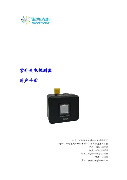
紫外光电探测器
用户手册
公司:成都诺为光科科技有限共你说
地址:四川省成都市领事馆路1号南谊大厦503室
电话:************
传真:************
邮箱:******************
邮编:610041
网址:
一、产品简介
紫外光电探测器是根据客户需求定制一套的具有高线性度、特定时间相应特性的新型光电探测设备。
采用了大靶面、紫外相应增强的滨松硅光半导体芯片。
探测器具有信号幅度高,线性度一致性强,噪声低的特点,配合专用直流电源工作,特别适合极紫外193nm波长区域的激光信号检测。
产品主要技术指标:
成都诺为光科科技有限公司
***安全警告***
成都诺为光科科技有限公司
成都诺为光科科技有限公司
二、使用方法
(1) 按照图示方法完成探测器与电源连接。
信号输出
(2) 打开电源通道开关,绿色指示灯亮起,探测器开始工作。
光电信号通过SMA 接口进行输出。
UV紫外线传感器系统方案技术参数(七巧智能科技)
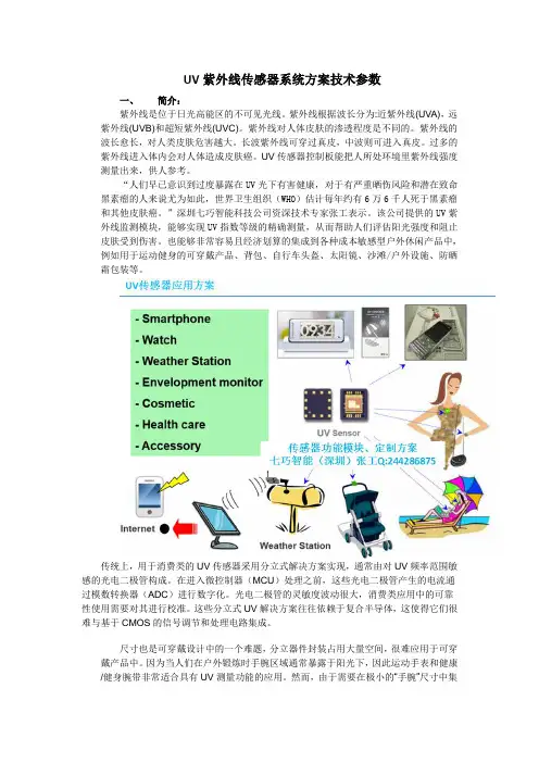
UV紫外线传感器系统方案技术参数一、简介:紫外线是位于日光高能区的不可见光线。
紫外线根据波长分为:近紫外线(UVA),远紫外线(UVB)和超短紫外线(UVC)。
紫外线对人体皮肤的渗透程度是不同的。
紫外线的波长愈长,对人类皮肤危害越大。
长波紫外线可穿过真皮,中波则可进入真皮。
过多的紫外线进入体内会对人体造成皮肤癌。
UV传感器控制板能把人所处环境里紫外线强度测量出来,供人参考。
“人们早已意识到过度暴露在UV光下有害健康,对于有严重晒伤风险和潜在致命黑素瘤的人来说尤为如此,世界卫生组织(WHO)估计每年约有6万6千人死于黑素瘤和其他皮肤癌。
”深圳七巧智能科技公司资深技术专家张工表示。
该公司提供的UV紫外线监测模块,能够实现UV指数等级的精确测量,从而帮助人们评估阳光强度和阻止皮肤受到伤害。
也能够非常容易且经济划算的集成到各种成本敏感型户外休闲产品中,例如用于运动健身的可穿戴产品、背包、自行车头盔、太阳镜、沙滩/户外设施、防晒霜包装等。
传统上,用于消费类的UV传感器采用分立式解决方案实现,通常由对UV频率范围敏感的光电二极管构成。
在进入微控制器(MCU)处理之前,这些光电二极管产生的电流通过模数转换器(ADC)进行数字化。
光电二极管的灵敏度波动很大,消费类应用中的可靠性使用需要对其进行校准。
这些分立式UV解决方案往往依赖于复合半导体,这使得它们很难与基于CMOS的信号调节和处理电路集成。
尺寸也是可穿戴设计中的一个难题,分立器件封装占用大量空间,很难应用于可穿戴产品中。
因为当人们在户外锻炼时手腕区域通常暴露于阳光下,因此运动手表和健康/健身腕带非常适合具有UV测量功能的应用。
然而,由于需要在极小的“手腕”尺寸中集成先进数字信号处理和天线功能,这些可穿戴设备已经变得空间极度受限。
二、核心芯片UV紫外线传感器ML8511,该产品运用绝缘上覆硅(SOI)-CMOS,为业界首款模拟电压输出、无滤光器的UV传感器。
ML8511_datasheet
捷多邦,您值得信赖的PCB打样专家!ML8511-00FCREFERENCE BOARD Manual for UV Sensor (QFN)Issue date: August 27, 2013NOTESNo copying or reproduction of this document, in part or in whole, is permitted without the consent of LAPIS Semiconductor Co., Ltd.The content specified herein is subject to change for improvement without notice.Examples of application circuits, circuit constants and any other information contained herein illustrate the standard usage and operations of the Products. The peripheral conditions must be taken into account when designing circuits for mass production.Great care was taken in ensuring the accuracy of the information specified in this document. However, should you incur any damage arising from any inaccuracy or misprint of such information, LAPIS Semiconductor shall bear no responsibility for such damage.The technical information specified herein is intended only to show the typical functions of and examples of application circuits for the Products. LAPIS Semiconductor does not grant you, explicitly or implicitly, any license to use or exercise intellectual property or other rights held by LAPIS Semiconductor and other parties. LAPIS Semiconductor shall bear no responsibility whatsoever for any dispute arising from the use of such technical information.The Products specified in this document are intended to be used with general-use electronic equipment or devices (such as audio visual equipment, office-automation equipment, communication devices, electronic appliances and amusement devices).The Products specified in this document are not designed to be radiation tolerant.While LAPIS Semiconductor always makes efforts to enhance the quality and reliability of its Products, a Product may fail or malfunction for a variety of reasons.Please be sure to implement in your equipment using the Products safety measures to guard against the possibility of physical injury, fire or any other damage caused in the event of the failure of any Product, such as derating, redundancy, fire control and fail-safe designs. LAPIS Semiconductor shall bear no responsibility whatsoever for your use of any Product outside of the prescribed scope or not in accordance with the instruction manual.The Products are not designed or manufactured to be used with any equipment, device or system which requires an extremely high level of reliability the failure or malfunction of which may result in a direct threat to human life or create a risk of human injury (such as a medical instrument, transportation equipment, aerospace machinery, nuclear-reactor controller, fuel-controller or other safety device). LAPIS Semiconductor shall bear no responsibility in any way for use of any of the Products for the above special purposes. If a Product is intended to be used for any such special purpose, please contact a ROHM sales representative before purchasing.If you intend to export or ship overseas any Product or technology specified herein that may be controlled under the Foreign Exchange and the Foreign Trade Law, you will be required to obtain a license or permit under the Law.Copyright 2013 LAPIS Semiconductor Co., Ltd.1. General DescriptionThe ML8511-00FC is a reference board for the Lapis Semiconductor UV Sensor ML8511. Below shows the FRONT and BACK of the PCB with a mounted ML8511 in a QFN package.2. Features∙UV Photodiode sensitive to UV-A and UV-B∙Embedded operational amplifier∙Analog voltage output∙Low supply current (300uA typ.) and low standby current (0.1uA typ.)∙Small SMT package (4.0mm x 3.7mm x 0.73mm, 12-pin ceramic QFN)∙Active high enable pin∙VDD input cap and reference voltage decoupling cap included on reference board3. ApplicationsSmart Phone, Watch, Weather station, Bicycle Navigation, Gaming, Health, Fitness, Accessories4. Recommended Operating ConditionsUnitMaximum Parameter Symbol MinimumTypicalOperating V oltage VDD 2.7 3.3 3.6 VOperating Temperature Ta -20 25 70 °CStorage Temperature Tstg -30 - 85 °C5. UV Sensor Optical FilterAn optical UV transmission filter is recommended with the usage of ML8511. The material recommended is ACRYLITE #000 (1.0mm thickness) with sandblast #220, if opaque filter is desired. The distance from ML8511 to filter is D1. D1 should be ~1.0mm. The aperture size of the filter is D2. D2 should be ~3.0mm.6. Output Voltage – UV CharacteristicsThe below chart shows the linear relationship between the sensor’s output voltage and UV intensity (mW/cm2) when Vdd = 3.0V. The sensor output is stable across the operating temperature range.7. Spectral Response CharacteristicsThe ML8511 has the spectral response of measuring UV A and UVB wavelengths. UV-A: 315-400nmUV-B: 280-315nm8. Reference Board SchematicThe schematic below shows the reference board inputs/outputs and pin connections.9. Reference Board Dimensions10. Table of Pin DescriptionsCN1 through-hole # Through-hole Name Function1 UVOUT Output2 UVEN Active high EN_pin (High: Active /Low: Standby)3 - -4 - -5 GND Ground6 - -7 - -8 - -9 - -V oltage10 VDD Input*Please refer to the ML8511 datasheet for additional details on electrical specifications andrecommendations.Revision HistoryPageDocument No. Issue Date PreviousEditionNewEditionDescriptionFEBL8511_REFBOARD_Manual-012013.08.27 – – First Edition。
紫外线传感器杀菌消毒原理解析
紫外线传感器杀菌消毒原理解析紫外线传感器只对185~260nm狭窄范围内的紫外线进行响应,而对其它频谱范围的光线不敏感,利用它可以对火焰中的紫外线进行检测。
它是一个封闭且能透过紫外线的玻璃管,管内充满了一种特殊的气体。
玻璃管内部有一对由金属引线引出的电极——阳极和光电阴极,其中光电阴极由只对紫外线敏感的金属材料制成,在紫外线照射下发射光电子。
紫外线消毒杀菌用途很广,医院、学校、托儿所、电影院、公交车、办公室、家庭等,它能净化空气,消除霉味,水质消毒,此外还能产生一定量的负氧离子,经紫外线消毒的房间,空气特别清新。
在公共场合,经紫外线消毒,可避免一些病菌经空气传播或经物体表面传播。
是利用适当波长的紫外线能够破坏微生物机体细胞中的DNA(脱氧核糖核酸)或RNA(核糖核酸)的分子结构,造成生长性细胞死亡和(或)再生性细胞死亡,达到杀菌消毒的效果。
经试验,紫外线杀菌的有效波长范围可分为四个不同的波段:UV A(400~315nm)、UVB(315~280nm)、UVC(280~200nm)和真空紫外线(200~100nm)。
其中能透过臭氧保护层和云层到达地球表面的只有UV A和UVB部分。
就杀菌速度而言,UVC处于微生物吸收峰范围之内,可在1s之内通过破坏微生物的DNA结构杀死病毒和细菌,而UV A 和UVB由于处于微生物吸收峰范围之外,杀菌速度很慢,往往需要数小时才能起到杀菌作用,在实际工程的数秒钟水力停留(照射)时间内,该部分实际上属于无效紫外部分。
真空紫外光穿透能力极弱,灯管和套管需要采用极高透光率的石英,一般用半导体行业降解水中的TOC,不用于杀菌消毒。
因此,给排水工程中所说的紫外光消毒实际上就是指UVC消毒。
紫外光消毒技术是基于现代防疫学、医学和光动力学的基础上,利用特殊设计的高效率、高强度和长寿命的UVC波段紫外光照射流水,将水中各种细菌、病毒、寄生虫、水藻以及其他病原体直接杀死,达到消毒的目的。
紫外传感器原理
紫外传感器原理
紫外传感器是一种可以测量环境中紫外线辐射强度的设备。
其基本原理是利用材料对紫外线的敏感性,将紫外线的能量转换为电信号。
紫外线传感器通常由一个光电二极管和一个滤光器组成。
光电二极管是一个半导体器件,当它受到紫外线照射时,就会产生电流。
滤光器的作用是选择性地过滤出特定波长的紫外线,阻挡其他波长的光线。
当紫外线照射到滤光器上时,只有特定波长的紫外线能透过滤光器,进入光电二极管。
光电二极管根据接收到的紫外线的强度产生一个电流。
这个电流的大小与紫外线的强弱成正比。
紫外传感器通常还配备一个放大电路和一个ADC(模数转换器)。
放大电路用来放大光电二极管产生的微弱电流,使得它可以被ADC检测到。
ADC将模拟电流信号转换成数字信号,以便进一步处理和分析。
通过测量紫外线的强度,紫外传感器可以用于多种应用。
例如,它可以用于测量紫外线的辐射量,以便判断环境中紫外线的强度是否达到了安全标准。
此外,紫外传感器还常用于紫外线灯的控制,例如在紫外线杀菌设备中,可以根据紫外传感器测量到的紫外线强度来控制灯的开启和关闭。
总之,紫外传感器利用光电二极管和滤光器的组合实现了对紫外线辐射强度的测量。
通过将紫外线能量转换为电信号,并经
过放大和转换处理,紫外传感器可以提供准确的紫外线强度测量结果,以支持各种应用需求。
紫外光辐照交联设备使用说明书
1)适用范围广 紫外光辐照交联设备均匀交联厚度能达到 20mm 以上,为普通交联聚乙烯电缆,阻燃交 联电缆等多种电缆的生产提供了可能性。生产速度高,以普通交联聚乙烯电缆为例,热延伸 稳定控制在 100%左右时,不同线径及标称绝缘厚度的生产速度参考图如下:
III
导体截面mm2 10 25 50 95 150 240 300
(内部电压为高压)。 若不遵守规定,将会导致死亡或严重伤害。
I
目录
1 概述............................................................................................................................................. 3 1.1 紫外光辐照交联设备的应用............................................................................................... 3 1.2 紫外光辐照交联设备特点........................................................................................... 3
使用寿命发挥到最大。
6)操作方便
紫外光辐照交联设备的使用请遵从调试人员指导并按照说明说的操作说明。设备的基本
操作包含:总电源上电/断电、开盖/合盖以及各组辐照灯源的开闭,操作简单易学,且部分
功能含有误操作保护。具体操作说明及注意事项请参照下文。
4
2 设备组成与认知
紫外光辐照交联设备组成部分包含:辐照主箱体、进/排风风机组、控制柜、灯源供电 柜。
紫外光杀菌液体处理器[实用新型专利]
专利名称:紫外光杀菌液体处理器专利类型:实用新型专利
发明人:邓培星
申请号:CN200520120003.5
申请日:20051202
公开号:CN2851252Y
公开日:
20061227
专利内容由知识产权出版社提供
摘要:本实用新型涉及一种紫外光杀菌液体处理器,包括筒状壳体(l)、置于壳体(1)内的紫外光灯管(2)和石英管灯罩(3),所述筒状壳体(1)上设置有进水管(11)和出水管(12),所述筒状壳体(l)与石英管灯罩(3)之间设有一圆筒状反光层(5)。
同现有技术相比较,本实用新型具有杀菌效果好、使用寿命长等优点。
申请人:深圳市兴日生实业有限公司
地址:518118 广东省深圳市龙岗区宝龙工业城宝龙大道三号路
国籍:CN
代理机构:深圳睿智专利事务所
代理人:陈鸿荫
更多信息请下载全文后查看。
- 1、下载文档前请自行甄别文档内容的完整性,平台不提供额外的编辑、内容补充、找答案等附加服务。
- 2、"仅部分预览"的文档,不可在线预览部分如存在完整性等问题,可反馈申请退款(可完整预览的文档不适用该条件!)。
- 3、如文档侵犯您的权益,请联系客服反馈,我们会尽快为您处理(人工客服工作时间:9:00-18:30)。
APPLICATIONS
• Smart phone, Watch, Weather station,Bicycle navigation, Accessary, Gaming
BLOCK DAIAGRAM
TP
9
VDD
7
EN
4
Amplifier
8
OUT
UV Photodiode ML8511
5 10
GND
15
SPECTRAL RESPONSIVILITY CHARACTERISTICS
1.0 Relative Responsivity 0.8 0.6 0.4 0.2 0.0 280 320 360 400 440
Ta=25°C, VDD=3.0V
480
520
560
Wavelength (nm)
4/8
Condition Ta=25 C Ta=25 C Ta=25 C Ta=25 C -
Rating -0.3 to +4.6 -0.3 to +4.6 5 30 -30 to +85
unit V V mA mW C
RECOMENTED OPERATION CONDITIONS
Parameter Operating Voltage Operating Temperature Symbol VDD Ta Min. 2.7 -20 Typ. 3.3 Max. 3.6 70 unit V C
FEDL8511-05
ML8511
TIMING CHART
Supply voltage and EN signal state should take one of the following procedures: 1. EN should be HIGH or LOW at the same time when VDD is applied. 2. EN should be HIGH or LOW while VDD is applied. Output should be read after output voltage level becomes stable. Maximum time required until stable output voltage reaches is 1 millisecond after EN goes HIGH.
1/8
FEDL8511-05
ML8511
EXAMPLE OF CONNCTING DIAGRAM
ML8511
7
VDD OUT
8
ADC PORT
0.1uF
5
EN GND TR
10
4
1nF
* Load resistance of OUT port is recommended more than 100 k.
3/8
FEDL8511-05
ML8511
OUTPUT VALTAGE– UV INTENSITY CHARCTERISTICS
3.5 3.0 Output Voltage (V) 2.5 2.0 1.5 1.0 0.5 0
VDD=3.0V
75 ℃ 25 ℃ -5 ℃ -25 ℃
3 6 9 12 2 UV Intensity (mW/cm ) @ λ365nm
TR
PIN CONFIGURATIONS
Pin 7 5 4 8 9 10 1,2,3, 6,11,12 Symbol VDD GND EN OUT TP TR NC I/O PW PW I O I/O I/O Function Supply voltage. Decouple this pin to ground with 0.1 F capacitor. Ground Active high enable pin. (High: Active mode, Low: Standby mode) Output (Low in power down or standby mode) Test pin. Do not connect. Internal reference voltage. Decouple this pin to ground with 1 nF capacitor. No Connection. Do not connect.
6/8
FEDL8511-05
ML8511
REVISON HISTORY
Document No. FEDL851100FC-01 FEDL8511-02 Date Sep. 3, 2008 Jan. 24, 2008 1 2 FEDL8511-03 Nov. 7, 2008 3 3 1 FJDL8511-04 Jan. 17, 2013 4 5 1 2 2 3 4 1 4 5 1 2 Page Previous Current Edition Edition 1 5 1 Description Preliminary edition Added disclaimer Changed Logo OKI to OKI SEMICONDUCTOR The following items has been moved: PACKAGE, NOTICE, PRECAUTION and DISCLAIMER. The following items have been moved: BLOCK DIAGRAM and PIN CONFIGRATION The following tables has been partially modified: RECOMMENDED OPERATING CONDITIONS ELECTRO-OPTICAL CHARACTERISTICS Changed load resistance 500 k to 100 k Added graphs Added “TIMING CHART” Feature description is removed. Applications section is added. Explanation is provided to the timing chart. Package drawing is updated. Descriptions in the NOTE are modified. DISCLIMER is removed. Descriptions in Pin configurations are modified. Example of connecting diagram is added.
Typ. 300 0.1 365 1.0 2.2
Max. 500 1 VDD + 0.3 0.72 1 1 1.05 2.32
unit A A V V A A nm ms V V
* Load resistance of OUT port is recommended more than 100 k.
FEATURES
• Photodiode sensitive to UV-A and UV-B • Embedded operational amplifier • Analog voltage output • Low supply current (300A typ.) and low standby current (0.1A typ.) • Small and thin surface mount package (4.0mm x 3.7mm x 0.73mm, 12-pin ceramic QFN)
VDD
EN TSU OUT
5/8
FEDL8511-05
ML8511
PACKAGE DIMENTIONS
(Unit: mm)
Notes for Mounting the Surface Mount Type Package The surface mount type packages are very susceptible to heat in reflow mounting and humidity absorbed in storage. Therefore, before you perform reflow mounting, contact our responsible sales person for the product name, package name, pin number, package code and desired mounting conditions (reflow method, temperature and times). Specifications are defined without considering the UV absorption by an external cover material. Please contact our sales representativeus when the cover material is applied. Do not press or rub the surface of the resin covering the top of the package where, which is on the UV-ray is light received. In addition, do not apply pressure at high temperature.
ELECTRO-OPTICAL CHARACTERISTICS
(VDD=+2.7V to +3.6V, Ta= -20C to +70C)
Parameter Supply Current (active mode) Supply Current (standby mode) Input Voltage (High level) Input Voltage (Low level) High level input current Low level input current Wavelength of maximum sensitivity Output Setup Time Output Voltage (Shading) * Output Voltage (10mW/cm at p) *