5082-G511-KK400中文资料
LM4040_05中文资料
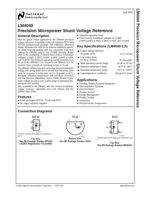
LM4040Precision Micropower Shunt Voltage ReferenceGeneral DescriptionIdeal for space critical applications,the LM4040precision voltage reference is available in the sub-miniature SC70and SOT-23surface-mount package.The LM4040’s advanced design eliminates the need for an external stabilizing capaci-tor while ensuring stability with any capacitive load,thus making the LM4040easy to use.Further reducing design effort is the availability of several fixed reverse breakdown voltages:2.048V,2.500V,3.000V,4.096V,5.000V,8.192V,and 10.000V.The minimum operating current increases from 60µA for the LM4040-2.5to 100µA for the LM4040-10.0.All versions have a maximum operating current of 15mA.The LM4040utilizes fuse and zener-zap reverse breakdown voltage trim during wafer sort to ensure that the prime parts have an accuracy of better than ±0.1%(A grade)at 25˚C.Bandgap reference temperature drift curvature correction and low dynamic impedance ensure stable reverse break-down voltage accuracy over a wide range of operating tem-peratures and currents.Also available is the LM4041with two reverse breakdown voltage versions:adjustable and 1.2V.Please see the LM4041data sheet.Featuresn Small packages:SOT-23,TO-92and SC70n No output capacitor requiredn Tolerates capacitive loadsn Fixed reverse breakdown voltages of 2.048V,2.500V,3.000V,4.096V,5.000V,8.192V,and 10.000VKey Specifications (LM4040-2.5)j Output voltage tolerance(A grade,25˚C)±0.1%(max)j Low output noise(10Hz to 10kHz)35µV rms (typ)j Wide operating current range 60µA to 15mA j Industrial temperature range −40˚C to +85˚C j Extended temperature range −40˚C to +125˚C j Low temperature coefficient100ppm/˚C (max)Applicationsn Portable,Battery-Powered Equipment n Data Acquisition Systems n Instrumentation n Process Controln Energy Management n Product Testing n AutomotivenPrecision Audio ComponentsConnection DiagramsSOT-23TO-92SC7001132301*This pin must be left floating or connected to pin 2.Top ViewSee NS Package Number MF03A (JEDEC Registration TO-236AB)01132303Bottom ViewSee NS Package Number Z03A01132330*This pin must be left floating or connected to pin1.Top ViewSee NS Package Number MAA05AApril 2005LM4040Precision Micropower Shunt Voltage Reference©2005National Semiconductor Corporation Ordering InformationIndustrial Temperature Range (−40˚C to +85˚C)Reverse Breakdown Voltage Tolerance at 25˚C and Average Reverse Breakdown Voltage Temperature CoefficientPackageNS Package NumberM3(SOT-23)M7(SC70)Z (TO-92)Supplied as 1000Units Tape andReelSupplied as 3000Units tape andReelSupplied as 1000Units Tape andReelSupplied as 3000Units Tape andReel±0.1%,100ppm/˚C max (A grade)LM4040AIM3-2.0LM4040AIM3-2.5LM4040AIM3-3.0LM4040AIM3-4.1LM4040AIM3-5.0LM4040AIM3-8.2LM4040AIM3-10.0LM4040AIM3X-2.0LM4040AIM3X-2.5LM4040AIM3X-3.0LM4040AIM3X-4.1LM4040AIM3X-5.0LM4040AIM3X-8.2LM4040AIM3X-10.0LM4040AIZ-2.0LM4040AIZ-2.5LM4040AIZ-3.0LM4040AIZ-4.1LM4040AIZ-5.0LM4040AIZ-8.2LM4040AIZ-10.0MF03A,Z03A±0.2%,100ppm/˚C max (B grade)LM4040BIM3-2.0LM4040BIM3-2.5LM4040BIM3-3.0LM4040BIM3-4.1LM4040BIM3-5.0LM4040BIM3-8.2LM4040BIM3-10.0LM4040BIM3X-2.0LM4040BIM3X-2.5LM4040BIM3X-3.0LM4040BIM3X-4.1LM4040BIM3X-5.0LM4040BIM3X-8.2LM4040BIM3X-10.0LM4040BIM7-2.0LM4040BIM7-2.5LM4040BIM7-3.0LM4040BIM7-4.1LM4040BIM7-5.0LM4040BIM7X-2.0LM4040BIM7X-2.5LM4040BIM7X-3.0LM4040BIM7X-4.1LM4040BIM7X-5.0LM4040BIZ-2.0LM4040BIZ-2.5LM4040BIZ-3.0LM4040BIZ-4.1LM4040BIZ-5.0LM4040BIZ-8.2LM4040BIZ-10.0MF03A,Z03A,MAA05A ±0.5%,100ppm/˚C max (C grade)LM4040CIM3-2.0LM4040CIM3-2.5LM4040CIM3-3.0LM4040CIM3-4.1LM4040CIM3-5.0LM4040CIM3-8.2LM4040CIM3-10.0LM4040CIM3X-2.0LM4040CIM3X-2.5LM4040CIM3X-3.0LM4040CIM3X-4.1LM4040CIM3X-5.0LM4040CIM3X-8.2LM4040CIM3X-10.0LM4040CIM7-2.0LM4040CIM7-2.5LM4040CIM7-3.0LM4040CIM7-4.1LM4040CIM7-5.0LM4040CIM7X-2.0LM4040CIM7X-2.5LM4040CIM7X-3.0LM4040CIM7X-4.1LM4040CIM7X-5.0LM4040CIZ-2.0LM4040CIZ-2.5LM4040CIZ-3.0LM4040CIZ-4.1LM4040CIZ-5.0LM4040CIZ-8.2LM4040CIZ-10.0MF03A,Z03A,MAA05A ±1.0%,150ppm/˚C max (D grade)LM4040DIM3-2.0LM4040DIM3-2.5LM4040DIM3-3.0LM4040DIM3-4.1LM4040DIM3-5.0LM4040DIM3-8.2LM4040DIM3-10.0LM4040DIM3X-2.0LM4040DIM3X-2.5LM4040DIM3X-3.0LM4040DIM3X-4.1LM4040DIM3X-5.0LM4040DIM3X-8.2LM4040DIM3X-10.0LM4040DIM7-2.0LM4040DIM7-2.5LM4040DIM7-3.0LM4040DIM7-4.1LM4040DIM7-5.0LM4040DIM7X-2.0LM4040DIM7X-2.5LM4040DIM7X-3.0LM4040DIM7X-4.1LM4040DIM7X-5.0LM4040DIZ-2.0LM4040DIZ-2.5LM4040DIZ-3.0LM4040DIZ-4.1LM4040DIZ-5.0LM4040DIZ-8.2LM4040DIZ-10.0MF03A,Z03A,MAA05A ±2.0%,150ppm/˚C max (E grade)LM4040EIM3-2.0LM4040EIM3-2.5LM4040EIM3-3.0LM4040EIM3X-2.0LM4040EIM3X-2.5LM4040EIM3X-3.0LM4040EIM7-2.0LM4040EIM7-2.5LM4040EIM7-3.0LM4040EIM7X-2.0LM4040EIM7X-2.5LM4040EIM7X-3.0LM4040EIZ-2.0LM4040EIZ-2.5LM4040EIZ-3.0MF03A,Z03A,MAA05AL M 4040 2Extended Temperature Range(−40˚C to+125˚C)Reverse BreakdownVoltage Tolerance at25˚C and Average Reverse Breakdown Voltage Temperature CoefficientPackageM3(SOT-23) See NS Package Number MF03A±0.5%,100ppm/˚C max(C grade)LM4040CEM3-2.0,LM4040CEM3-2.5,LM4040CEM3-3.0,LM4040CEM3-5.0±1.0%,150ppm/˚C max(D grade)LM4040DEM3-2.0,LM4040DEM3-2.5,LM4040DEM3-3.0,LM4040DEM3-5.0±2.0%,150ppm/˚C max(E grade)LM4040EEM3-2.0,LM4040EEM3-2.5,LM4040EEM3-3.0LM40403SOT-23AND SC70Package Marking InformationOnly three fields of marking are possible on the SOT-23’s and SC70’s small surface.This table gives the meaning of the three fields.Part Marking Field DefinitionRJA SOT-23only First Field:R2A SOT-23only RKA SOT-23only R4A SOT-23only R =Reference R5A SOT-23onlySecond Field:J =2.048V Voltage Option 2=2.500V Voltage OptionR8A SOT-23only K =3.000V Voltage Option R0A SOT-23only4=4.096V Voltage Option RJB R2B 5=5.000V Voltage Option RKB R4B 8=8.192V Voltage Option R5B 0=10.000V Voltage Option R8B SOT-23only R0B SOT-23onlyThird Field:RJC R2C A–E =Initial Reverse Breakdown Voltage or Reference Voltage Tolerance RKC R4C A =±0.1%,B =±0.2%,C =+0.5%,D =±1.0%,E =±2.0%R5C R8C SOT-23only R0C SOT-23onlyRJD R2D RKD R4D R5D R8D SOT-23only R0D SOT-23onlyRJE R2E RKEL M 4040 4Absolute Maximum Ratings(Note1)If Military/Aerospace specified devices are required, please contact the National Semiconductor Sales Office/ Distributors for availability and specifications. Reverse Current20mA Forward Current10mA Power Dissipation(T A=25˚C)(Note2)M3Package306mW Z Package550mW M7Package241mW Storage Temperature−65˚C to+150˚C Lead TemperatureM3PackageVapor phase(60seconds)+215˚C Infrared(15seconds)+220˚C Z PackageSoldering(10seconds)+260˚C ESD SusceptibilityHuman Body Model(Note3)2kVMachine Model(Note3)200V See AN-450“Surface Mounting Methods and Their Effect on Product Reliability”for other methods of soldering surface mount devices.Operating Ratings(Notes1,2) Temperature Range(T min≤T A≤T max) Industrial Temperature Range−40˚C≤T A≤+85˚C Extended Temperature Range−40˚C≤T A≤+125˚C Reverse CurrentLM4040-2.060µA to15mA LM4040-2.560µA to15mA LM4040-3.062µA to15mA LM4040-4.168µA to15mA LM4040-5.074µA to15mA LM4040-8.291µA to15mA LM4040-10.0100µA to15mALM4040-2.0Electrical Characteristics(Industrial Temperature Range)Boldface limits apply for T A=T J=T MIN to T MAX;all other limits T A=T J=25˚C.The grades A and B designate initial Re-verse Breakdown Voltage tolerances of±0.1%and±0.2%,respectively.Symbol Parameter Conditions Typical(Note4)LM4040AIM3LM4040AIZ(Limit)(Note5)LM4040BIM3LM4040BIZLM4040BIM7(Limit)(Note5)Units(Limit)V R Reverse Breakdown Voltage I R=100µA 2.048VReverse Breakdown Voltage Tolerance(Note6)I R=100µA±2.0±4.1mV(max)±15±17mV(max)I RMIN Minimum Operating Current45µA6060µA(max)6565µA(max)∆V R/∆T Average Reverse BreakdownVoltage TemperatureCoefficient(Note6)I R=10mA±20ppm/˚CI R=1mA±15±100±100ppm/˚C(max) I R=100µA±15ppm/˚C∆V R/∆I R Reverse Breakdown VoltageChange with OperatingCurrent Change(Note*NOTARGET FOR*)I RMIN≤I R≤1mA0.3mV0.80.8mV(max)1.0 1.0mV(max) 1mA≤I R≤15mA2.5mV6.0 6.0mV(max)8.08.0mV(max)Z R Reverse DynamicImpedance I R=1mA,f=120Hz,I AC=0.1I R0.3Ω0.80.8Ω(max)e N Wideband Noise I R=100µA35µV rms10Hz≤f≤10kHzLM40405LM4040-2.0Electrical Characteristics (Industrial Temperature Range)(Continued)Boldface limits apply for T A =T J =T MIN to T MAX ;all other limits T A =T J =25˚C.The grades A and B designate initial Re-verse Breakdown Voltage tolerances of ±0.1%and ±0.2%,respectively.Symbol Parameter ConditionsTypical (Note 4)LM4040AIM3LM4040AIZ (Limit)(Note 5)LM4040BIM3LM4040BIZ LM4040BIM7(Limit)(Note 5)Units (Limit)∆V RReverse Breakdown Voltage Long Term Stability t =1000hrs T =25˚C ±0.1˚CI R =100µA 120ppmV HYSTThermal Hysteresis (Note 8)∆T =−40˚C to +125˚C0.08%LM4040-2.0Electrical Characteristics (Industrial Temperature Range)Boldface limits apply for T A =T J =T MIN to T MAX ;all other limits T A =T J =25˚C.The grades C,D and E designate initial Reverse Breakdown Voltage tolerances of ±0.5%,±1.0%and ±2.0%,respectively.SymbolParameterConditionsTypical (Note 4)LM4040CIM3LM4040CIZ LM4040CIM7(Limit)(Note 5)LM4040DIM3LM4040DIZ LM4040DIM7(Limit)(Note 5)LM4040EIM7LM4040EIZ (Limit)(Note 5)Units(Limit)V RReverse Breakdown VoltageI R =100µA 2.048VReverse Breakdown Voltage Tolerance (Note 6)I R =100µA ±10±20±41mV (max)±23±40±60mV (max)I RMINMinimum Operating Current45µA 606565µA (max)657070µA (max)∆V R /∆TAverage Reverse Breakdown Voltage Temperature Coefficient (Note 6)I R =10mA ±20ppm/˚CI R =1mA ±15±100±150±150ppm/˚C (max)I R =100µA±15ppm/˚C ∆V R /∆I RReverse Breakdown Voltage Change with Operating Current Change (Note *NO TARGET FOR *)I RMIN ≤I R ≤1mA 0.3mV 0.8 1.0 1.0mV (max)1.01.21.2mV (max)1mA ≤I R ≤15mA 2.5mV 6.08.08.0mV (max)8.010.010.0mV (max)Z R Reverse Dynamic Impedance I R =1mA,f =120Hz 0.3ΩI AC =0.1I R 0.91.11.1Ω(max)e N Wideband NoiseI R =100µA 35µV rms10Hz ≤f ≤10kHz∆V RReverse Breakdown Voltage Long Term Stability t =1000hrsT =25˚C ±0.1˚C 120ppmI R =100µA V HYSTThermal Hysteresis (Note 8)∆T =−40˚C to +125˚C0.08%L M 4040 6LM4040-2.0Electrical Characteristics(Extended Temperature Range)Boldface limits apply for T A=T J=T MIN to T MAX;all other limits T A=T J=25˚C.The grades C,D and E designate initial Reverse Breakdown Voltage tolerances of±0.5%,±1.0%and±2.0%,respectively.Symbol Parameter Conditions Typical(Note4)LM4040CEM3(Limit)(Note5)LM4040DEM3(Limit)(Note5)LM4040EEM3(Limit)(Note5)Units(Limit)V R Reverse BreakdownVoltageI R=100µA 2.048VReverse Breakdown Voltage Tolerance (Note6)I R=100µA±10±20±41mV(max)±30±50±70mV(max)I RMIN Minimum OperatingCurrent 45µA606565µA(max)687373µA(max)∆V R/∆T Average ReverseBreakdown VoltageTemperatureCoefficient(Note6)I R=10mA±20ppm/˚CI R=1mA±15±100±150±150ppm/˚C(max) I R=100µA±15ppm/˚C∆V R/∆I R Reverse BreakdownVoltage Change withOperating CurrentChange(Note7)I RMIN≤I R≤1mA0.3mV0.8 1.0 1.0mV(max)1.0 1.2 1.2mV(max) 1mA≤I R≤15mA2.5mV6.08.08.0mV(max)8.010.010.0mV(max)Z R Reverse DynamicImpedance I R=1mA,f=120Hz,I AC=0.1I R0.3Ω0.9 1.1 1.1Ω(max)e N Wideband Noise I R=100µA35µV rms10Hz≤f≤10kHz∆V R Reverse BreakdownVoltage Long TermStability t=1000hrsT=25˚C±0.1˚CI R=100µA120ppmV HYST Thermal Hysteresis(Note8)∆T=−40˚C to+125˚C0.08%LM4040-2.5Electrical Characteristics(Industrial Temperature Range)Boldface limits apply for T A=T J=T MIN to T MAX;all other limits T A=T J=25˚C.The grades A and B designate initial Re-verse Breakdown Voltage tolerances of±0.1%and±0.2%,respectively.Symbol Parameter Conditions Typical(Note4)LM4040AIM3LM4040AIZ(Limit)(Note5)LM4040BIM3LM4040BIZLM4040BIM7Limits(Note5)Units(Limit)V R Reverse Breakdown Voltage I R=100µA 2.500VReverse Breakdown Voltage Tolerance(Note6)I R=100µA±2.5±5.0mV(max)±19±21mV(max)I RMIN Minimum Operating Current45µA6060µA(max)6565µA(max)LM40407LM4040-2.5Electrical Characteristics (Industrial Temperature Range)(Continued)Boldface limits apply for T A =T J =T MIN to T MAX ;all other limits T A =T J =25˚C.The grades A and B designate initial Re-verse Breakdown Voltage tolerances of ±0.1%and ±0.2%,respectively.Symbol Parameter ConditionsTypical (Note 4)LM4040AIM3LM4040AIZ (Limit)(Note 5)LM4040BIM3LM4040BIZ LM4040BIM7Limits (Note 5)Units (Limit)∆V R /∆TAverage Reverse Breakdown Voltage Temperature Coefficient (Note 6)I R =10mA ±20ppm/˚CI R =1mA ±15±100±100ppm/˚C (max)I R =100µA±15ppm/˚C ∆V R /∆I R Reverse Breakdown Voltage Change with Operating Current Change (Note 7)I RMIN ≤I R ≤1mA0.3mV0.80.8mV (max)1.01.0mV (max)1mA ≤I R ≤15mA2.5mV 6.0 6.0mV (max)8.08.0mV (max)Z R Reverse Dynamic Impedance I R =1mA,f =120Hz,I AC =0.1I R 0.3Ω0.80.8Ω(max)e N Wideband NoiseI R =100µA 35µV rms10Hz ≤f ≤10kHz∆V RReverse Breakdown Voltage Long Term Stability t =1000hrs T =25˚C ±0.1˚CI R =100µA 120ppmV HYSTThermal Hysteresis (Note 8)∆T =−40˚C to +125˚C0.08%LM4040-2.5Electrical Characteristics (Industrial Temperature Range)Boldface limits apply for T A =T J =T MIN to T MAX ;all other limits T A =T J =25˚C.The grades C,D and E designate initial Reverse Breakdown Voltage tolerances of ±0.5%,±1.0%and ±2.0%,respectively.SymbolParameterConditionsTypical (Note 4)LM4040CIM3LM4040DIZ LM4040CIM7Limits (Note 5)LM4040DIM3LM4040DIZ LM4040DIM7Limits (Note 5)LM4040EIM7LM4040EIZ Limits(Note 5)Units(Limit)V RReverse Breakdown VoltageI R =100µA 2.500VReverse Breakdown Voltage Tolerance (Note 6)I R =100µA ±12±25±50mV (max)±29±49±74mV (max)I RMINMinimum Operating Current45µA 606565µA (max)657070µA (max)∆V R /∆TAverage Reverse Breakdown Voltage TemperatureCoefficient(Note 6)I R =10mA ±20ppm/˚C I R =1mA ±15±100±150±150ppm/˚C (max)I R =100µA±15ppm/˚CL M 4040 8LM4040-2.5Electrical Characteristics(Industrial Temperature Range)(Continued)Boldface limits apply for T A=T J=T MIN to T MAX;all other limits T A=T J=25˚C.The grades C,D and E designate initial Reverse Breakdown Voltage tolerances of±0.5%,±1.0%and±2.0%,respectively.Symbol Parameter Conditions Typical(Note4)LM4040CIM3LM4040DIZLM4040CIM7Limits(Note5)LM4040DIM3LM4040DIZLM4040DIM7Limits(Note5)LM4040EIM7LM4040EIZLimits(Note5)Units(Limit)∆V R/∆I R Reverse BreakdownVoltage Change withOperating CurrentChange(Note7)I RMIN≤I R≤1mA0.3mV0.8 1.0 1.0mV(max)1.0 1.2 1.2mV(max) 1mA≤I R≤15mA2.5mV6.08.08.0mV(max)8.010.010.0mV(max)Z R Reverse DynamicImpedance I R=1mA,f=120Hz0.3ΩI AC=0.1I R0.9 1.1 1.1Ω(max)e N Wideband Noise I R=100µA35µV rms10Hz≤f≤10kHz∆V R Reverse BreakdownVoltage Long TermStability t=1000hrsT=25˚C±0.1˚C120ppm I R=100µAV HYST Thermal Hysteresis(Note8)∆T=−40˚C to+125˚C0.08%LM4040-2.5Electrical Characteristics(Extended Temperature Range)Boldface limits apply for T A=T J=T MIN to T MAX;all other limits T A=T J=25˚C.The grades C,D and E designate initial Reverse Breakdown Voltage tolerances of±0.5%,±1.0%and±2.0%,respectively.Symbol Parameter Conditions Typical(Note4)LM4040CEM3Limits(Note5)LM4040DEM3Limits(Note5)LM4040EEM3Limits(Note5)Units(Limit)V R Reverse BreakdownVoltageI R=100µA 2.500VReverse Breakdown VoltageTolerance(Note6)I R=100µA±12±25±50mV(max)±38±63±88mV(max)I RMIN Minimum OperatingCurrent 45µA606565µA(max)687373µA(max)∆V R/∆T Average ReverseBreakdown VoltageTemperatureCoefficient(Note6)I R=10mA±20ppm/˚CI R=1mA±15±100±150±150ppm/˚C(max) I R=100µA±15ppm/˚C∆V R/∆I R Reverse BreakdownVoltage Change withOperating CurrentChange(Note7)I RMIN≤I R≤1mA0.3mV0.8 1.0 1.0mV(max)1.0 1.2 1.2mV(max)1mA≤I R≤15mA 2.5mV6.08.08.0mV(max)8.010.010.0mV(max)LM40409LM4040-2.5Electrical Characteristics (Extended Temperature Range)(Continued)Boldface limits apply for T A =T J =T MIN to T MAX ;all other limits T A =T J =25˚C.The grades C,D and E designate initial Reverse Breakdown Voltage tolerances of ±0.5%,±1.0%and ±2.0%,respectively.SymbolParameterConditionsTypical (Note 4)LM4040CEM3Limits (Note 5)LM4040DEM3Limits (Note 5)LM4040EEM3Limits (Note 5)Units(Limit)Z R Reverse Dynamic Impedance I R =1mA,f =120Hz,I AC =0.1I R 0.3Ω0.91.11.1Ω(max)e N Wideband NoiseI R =100µA 35µV rms10Hz ≤f ≤10kHz∆V RReverse Breakdown Voltage Long Term Stabilityt =1000hrsT =25˚C ±0.1˚CI R =100µA 120ppmV HYSTThermal Hysteresis(Note 8)∆T =−40˚C to +125˚C0.08%LM4040-3.0Electrical Characteristics (Industrial Temperature Range)Boldface limits apply for T A =T J =T MIN to T MAX ;all other limits T A =T J =25˚C.The grades A and B designate initial Re-verse Breakdown Voltage tolerances of ±0.1%and ±0.2%,respectively.Symbol Parameter ConditionsTypical (Note 4)LM4040AIM3LM4040AIZ (Limit)(Note 5)LM4040BIM3LM4040BIZ LM4040BIM7Limits (Note 5)Units (Limit)V R Reverse Breakdown Voltage I R =100µA 3.000VReverse Breakdown Voltage Tolerance (Note 6)I R =100µA ±3.0±6.0mV (max)±22±26mV (max)I RMINMinimum Operating Current47µA 6262µA (max)6767µA (max)∆V R /∆TAverage Reverse Breakdown Voltage Temperature Coefficient (Note 6)I R =10mA ±20ppm/˚C I R =1mA ±15±100±100ppm/˚C (max)I R =100µA±15ppm/˚C ∆V R /∆I R Reverse Breakdown Voltage Change with Operating Current Change (Note 7)I RMIN ≤I R ≤1mA0.6mV0.80.8mV (max)1.11.1mV (max)1mA ≤I R ≤15mA2.7mV 6.0 6.0mV (max)9.09.0mV (max)Z R Reverse Dynamic Impedance I R =1mA,f =120Hz,I AC =0.1I R 0.4Ω0.90.9Ω(max)e N Wideband NoiseI R =100µA 35µV rms10Hz ≤f ≤10kHz∆V RReverse Breakdown Voltage Long Term Stability t =1000hrs T =25˚C ±0.1˚CI R =100µA 120ppmV HYSTThermal Hysteresis (Note 8)∆T =−40˚C to +125˚C0.08%L M 4040 10LM4040-3.0Electrical Characteristics(Industrial Temperature Range)Boldface limits apply for T A=T J=T MIN to T MAX;all other limits T A=T J=25˚C.The grades C,D and E designate initial Reverse Breakdown Voltage tolerances of±0.5%,±1.0%and±2.0%,respectively.Symbol Parameter Conditions Typical(Note4)LM4040CIM3LM4040DIZLM4040CIM7Limits(Note5)LM4040DIM3LM4040DIZLM4040DIM7Limits(Note5)LM4040EIM7LM4040EIZLimits(Note5)Units(Limit)V R Reverse BreakdownVoltageI R=100µA 3.000VReverse Breakdown Voltage Tolerance (Note6)I R=100µA±15±30±60mV(max)±34±59±89mV(max)I RMIN Minimum OperatingCurrent 45µA606565µA(max)657070µA(max)∆V R/∆T Average ReverseBreakdown VoltageTemperatureCoefficient(Note6)I R=10mA±20ppm/˚CI R=1mA±15±100±150±150ppm/˚C(max) I R=100µA±15ppm/˚C∆V R/∆I R Reverse BreakdownVoltage Change withOperating CurrentChange(Note7)I RMIN≤I R≤1mA0.4mV0.8 1.1 1.1mV(max)1.1 1.3 1.3mV(max) 1mA≤I R≤15mA2.7mV6.08.08.0mV(max)9.011.011.0mV(max)Z R Reverse DynamicImpedance I R=1mA,f=120Hz0.4ΩI AC=0.1I R0.9 1.2 1.2Ω(max)e N Wideband Noise I R=100µA35µV rms10Hz≤f≤10kHz∆V R Reverse BreakdownVoltage Long TermStability t=1000hrsT=25˚C±0.1˚C120ppm I R=100µAV HYST Thermal Hysteresis(Note8)∆T=−40˚C to+125˚C0.08%LM4040-3.0Electrical Characteristics(Extended Temperature Range)Boldface limits apply for T A=T J=T MIN to T MAX;all other limits T A=T J=25˚C.The grades C,D and E designate initial Reverse Breakdown Voltage tolerances of±0.5%,±1.0%and±2.0%,respectively.Symbol Parameter Conditions Typical(Note4)LM4040CEM3Limits(Note5)LM4040DEM3Limits(Note5)LM4040EEM3Limits(Note5)Units(Limit)V R Reverse BreakdownVoltageI R=100µA 3.000VReverse Breakdown VoltageTolerance(Note6)I R=100µA±15±30±60mV(max)±45±75±105mV(max)I RMIN Minimum OperatingCurrent 47µA626767µA(max)707575µA(max)LM4040LM4040-3.0Electrical Characteristics (Extended Temperature Range)(Continued)Boldface limits apply for T A =T J =T MIN to T MAX ;all other limits T A =T J =25˚C.The grades C,D and E designate initial Reverse Breakdown Voltage tolerances of ±0.5%,±1.0%and ±2.0%,respectively.SymbolParameterConditionsTypical (Note 4)LM4040CEM3Limits (Note 5)LM4040DEM3Limits (Note 5)LM4040EEM3Limits (Note 5)Units(Limit)∆V R /∆TAverage Reverse Breakdown Voltage TemperatureCoefficient (Note 6)I R =10mA ±20ppm/˚CI R =1mA ±15±100±150±150ppm/˚C (max)I R =100µA±15ppm/˚C ∆V R /∆I R Reverse Breakdown Voltage Change with Operating Current Change (Note 7)I RMIN ≤I R ≤1mA0.4mV 0.8 1.1 1.1mV (max)1.11.31.3mV (max)1mA ≤I R ≤15mA2.7mV 6.08.08.0mV (max)9.011.011.0mV (max)Z R Reverse Dynamic Impedance I R =1mA,f =120Hz,I AC =0.1I R 0.4Ω0.91.21.2Ω(max)e N Wideband NoiseI R =100µA 35µV rms10Hz ≤f ≤10kHz∆V RReverse Breakdown Voltage Long Term Stabilityt =1000hrsT =25˚C ±0.1˚CI R =100µA 120ppmV HYSTThermal Hysteresis(Note 8)∆T =−40˚C to +125˚C0.08%LM4040-4.1Electrical Characteristics (Industrial Temperature Range)Boldface limits apply for T A =T J =T MIN to T MAX ;all other limits T A =T J =25˚C.The grades A and B designate initial Re-verse Breakdown Voltage tolerances of ±0.1%and ±0.2%,respectively.SymbolParameterConditionsTypical (Note 4)LM4040AIM3LM4040AIZ Limits (Note 5)LM4040BIM3LM4040BIZ LM4040BIM7Limits (Note 5)Units (Limit)V R Reverse Breakdown Voltage I R =100µA 4.096VReverse Breakdown Voltage Tolerance (Note 6)I R =100µA ±4.1±8.2mV (max)±31±35mV (max)I RMINMinimum Operating Current50µA 6868µA (max)7373µA (max)∆V R /∆TAverage Reverse Breakdown Voltage Temperature Coefficient(Note 6)I R =10mA ±30ppm/˚C I R =1mA ±20±100±100ppm/˚C (max)I R =100µA±20ppm/˚C ∆V R /∆I R Reverse Breakdown Voltage Change with Operating Current Change (Note 7)I RMIN ≤I R ≤1mA0.5mV0.90.9mV (max)1.21.2mV (max)1mA ≤I R ≤15mA3.0mV 7.07.0mV (max)10.010.0mV (max)L M 4040LM4040-4.1Electrical Characteristics(Industrial Temperature Range)(Continued)Boldface limits apply for T A=T J=T MIN to T MAX;all other limits T A=T J=25˚C.The grades A and B designate initial Re-verse Breakdown Voltage tolerances of±0.1%and±0.2%,respectively.Symbol Parameter Conditions Typical(Note4)LM4040AIM3LM4040AIZLimits(Note5)LM4040BIM3LM4040BIZLM4040BIM7Limits(Note5)Units(Limit)Z R Reverse DynamicImpedance I R=1mA,f=120Hz,0.5ΩI AC=0.1I R 1.0 1.0Ω(max)e N Wideband Noise I R=100µA80µV rms10Hz≤f≤10kHz∆V R Reverse Breakdown VoltageLong Term Stability t=1000hrsT=25˚C±0.1˚CI R=100µA120ppmV HYST Thermal Hysteresis(Note8)∆T=−40˚C to+125˚C0.08%LM4040LM4040-4.1Electrical Characteristics (Industrial Temperature Range)Boldface limits apply for T A =T J =T MIN to T MAX ;all other limits T A =T J =25˚C.The grades C and D designate initial Re-verse Breakdown Voltage tolerances of ±0.5%and ±1.0%,respectively.SymbolParameterConditionsTypical (Note 4)LM4040CIM3LM4040CIZ LM4040CIM7Limits (Note 5)LM4040DIM3LM4040BIZ LM4040DIM7Limits (Note 5)Units (Limit)V R Reverse Breakdown Voltage I R =100µA 4.096VReverse Breakdown Voltage Tolerance (Note 6)I R =100µA ±20±41mV (max)±47±81mV (max)I RMINMinimum Operating Current50µA 6873µA (max)7378µA (max)∆V R /∆T Average Reverse Breakdown Voltage Temperature Coefficient (Note 6)I R =10mA±30ppm/˚C I R =1mA ±20±100±150ppm/˚C (max)I R =100µA ±20ppm/˚C ∆V R /∆I R Reverse Breakdown Voltage Change with Operating Current Change (Note 7)I RMIN ≤I R ≤1mA 0.5mV0.9 1.2mV (max)1.21.5mV (max)1mA ≤I R ≤15mA3.0mV 7.09.0mV (max)10.013.0mV (max)Z R Reverse Dynamic Impedance I R =1mA,f =120Hz,0.5ΩI AC =0.1I R 1.01.3Ω(max)e N Wideband NoiseI R =100µA 80µV rms 10Hz ≤f ≤10kHz∆V RReverse Breakdown Voltage Long Term Stability t =1000hrs T =25˚C ±0.1˚CI R =100µA 120ppmV HYSTThermal Hysteresis (Note 8)∆T =−40˚C to +125˚C0.08%L M 4040LM4040-5.0Electrical Characteristics(Industrial Temperature Range)Boldface limits apply for T A=T J=T MIN to T MAX;all other limits T A=T J=25˚C.The grades A and B designate initial Re-verse Breakdown Voltage tolerances of±0.1%and±0.2%,respectively.Symbol Parameter Conditions Typical(Note4)LM4040AIM3LM4040AIZLimits(Note5)LM4040BIM3LM4040BIZLM4040BIM7Limits(Note5)Units(Limit)V R Reverse Breakdown Voltage I R=100µA 5.000VReverse Breakdown Voltage Tolerance(Note6)I R=100µA±5.0±10mV(max)±38±43mV(max)I RMIN Minimum Operating Current54µA7474µA(max)8080µA(max)∆V R/∆T Average Reverse Breakdown Voltage TemperatureCoefficient(Note6)I R=10mA±30ppm/˚CI R=1mA±20±100±100ppm/˚C(max) I R=100µA±20ppm/˚C∆V R/∆I R Reverse Breakdown VoltageChange with OperatingCurrent Change(Note7)I RMIN≤I R≤1mA0.5mV1.0 1.0mV(max)1.4 1.4mV(max) 1mA≤I R≤15mA 3.5mV8.08.0mV(max)12.012.0mV(max)Z R Reverse DynamicImpedance I R=1mA,f=120Hz,0.5ΩI AC=0.1I R 1.1 1.1Ω(max)e N Wideband Noise I R=100µA80µV rms10Hz≤f≤10kHz∆V R Reverse Breakdown VoltageLong Term Stability t=1000hrsT=25˚C±0.1˚C120ppm I R=100µAV HYST Thermal Hysteresis(Note8)∆T=−40˚C to+125˚C0.08%LM4040。
SKKT500中文资料

6748 , 2 73 9%+ -::, "44;47 -:: "44;47 -::, "44;6# -:: "44;6# -::, "44;6< -:: "44;6< -::, "44;6 -:: "44;6 -::, "44;67 -:: "44;67
SKKT 500, SKKH 500
Fig. 1L Power dissipation per thyristor vs. on-state current
Fig. 1R Power dissipation per thyristor vs. ambient temp.
Fig. 2L Power dissipation per module vs. rms current
Fig. 6 Transient thermal impedance vs. time
Fig. 7 On-state-characteristics
Fig. 8 Surge overload current vs. time
3
18-07-2005 HER
© by SEMIKRON
元器件交易网
8 ;
6748 ; 6#48 ; ;
Values
"<4 *!34 + " ; 7<" 7"4 ; ! A =4 6=444 6"444 6<<"444 66#"444 5 6" 5 43#" 5 4#= 5 644 6 # 5 #44 5 6444 644 #44 6"4 ; "44 !44 ; #444
MCCSEMI MF400K04F3产品说明说明书

Features•Lead Free Finish/RoHS Compliant (NOTE 1)("P" Suffix •designates RoHS Compliant. See ordering information)•Soft Reverse Recovery Characteristics •Ultrafast Reverse Recovery Time •Low Reverse Recovery Loss •Low Forward Voltage•High Surge Current Capability •Low Inductance PackageNote:1. High Temperature Solder Exemptions Applied, See EU Directive Annex 7a.Applications•Inversion Welder•Uninterruptible Power Supply (UPS)•Plating Power Supply•Ultrasonic Cleaner and Welder•Power Factor Correction (PFC) Circuit •Converter & Chopper400 Amp FRED Modules 400 VoltsMaximum Ratings SymbolConditions ValuesUnitsV R 400 V V RRM400 V I F(AV) T C =125°C, Per Diode200 A T C =125°C, Per Moudle 400 A T C =125°C, 20KHz, Per Moudle300 A I F(RMS) T C =125°C, Per Diode 285 A I FSM 1/2 Cycle , 50Hz, Sine 4000 A 1/2 Cycle , 60Hz, Sine 4500 A I 2t T J =45°C, t=10ms, 50Hz, Sine 80000 A 2s T J =45°C, t=8.3ms, 60Hz, Sine101250 A 2s P D 2080 W T J -40 to +150°C T STG -40 to +125°C Torque Recommended (M6) 3~4.7 N·m Torque Recommended (M6)3~4.7 N·m Weight92gThermal Characteristics Symbol Conditions Values UnitsR th(j-c)0.06 ℃/WElectrical CharacteristicsSymbolConditionsUnitsValuesMin.Typ.Max. I RM V R =400V -- -- 1 mA V R =400V, T J =125°C-- -- 2 mA V F I F =200A -- 1.1 1.35 V I F =200A, T J =125°C -- 1.0 1.25 V trr I F =1A, V R =30V, di F /dt=-200A/μs -- 45 -- ns trr V R =200V, I F =200A,di F /dt=-200A/μs, T J =25°C -- 135 -- ns I RRM -- 12 -- A trr V R =200V, I F =200A,di F /dt=-200A/μs, T J =125°C-- 210 -- ns I RRM--20--APerformance CurvesFig3. Reverse Recovery Current vs di F /dtFig4. Reverse Recovery Charge vs di F /dt0 V F 0.2 0.4 0.6 0.8 1.0 1.2 V 1.4Fig1. Forward Voltage Drop vs Forward CurrentFig2. Reverse Recovery Time vs di F /dt0 di F /dt 400 600600s 100025℃125℃V R =200V T J =125℃0 di F /dt500A/us 1000V R =200V T J =125℃I F =400A I F =200A I F =100AI F =400A I F =200A I F =100A0 di F /dt500A/us 1000 I F =400A I F =200A I F =100AV R =200V T J =125℃Fig5. Transient Thermal Impedance10-410-310-210-11Ordering InformationDevice PackingPart Number-BPBulk: 10PCS/BOX ;100PCS/CTN***IMPORTANT NOTICE***Micro Commercial Components Corp. reserves the right to make changes without further notice to any product herein to make corrections, modifications , enhancements , improvements , or other changes . Micro Commercial Components Corp . does not assume any liability arising out of the application or use of any product described herein; neither does it convey any license under its patent rights ,nor the rights of others . The user of products in such applications shall assume all risks of such use and will agree to hold Micro Commercial Components Corp . and all the companies whose products are represented on our website, harmless against all damages.***LIFE SUPPORT***MCC's products are not authorized for use as critical components in life support devices or systems without the expresswritten approval of Micro Commercial Components Corporation.***CUSTOMER AWARENESS***Counterfeiting of semiconductor parts is a growing problem in the industry. Micro Commercial Components (MCC) is taking strong measures to protect ourselves and our customers from the proliferation of counterfeit parts. MCC strongly encourages customers to purchase MCC parts either directly from MCC or from Authorized MCC Distributors who are listed by country on our web page cited below. Products customers buy either from MCC directly or from Authorized MCC Distributors are genuine parts, have full traceability, meet MCC's quality standards for handling and storage. MCC will not provide any warranty coverage or other assistance for parts bought from Unauthorized Sources. MCC is committed to combat this global problem and encourage our customers to do their part in stopping this practice by buying direct or from authorized distributors.。
1.5KE400A,TVS瞬变二极管中文资料

POWER: 1500Wa t VOLTAGE RANGE: 6.8 - 440 VAXIAL LEADED TRANSIENT VOLTAGE SUPPRESS DIODE1.5KE6.8A(CA) - 1.5KE440A(CA)6.8V – 440V Standoff VoltageCase: JEDEC DO-201AD Molded Plastic FeaturesGlass Passivated Die Construction Uni- and Bi-Directional Versions Available Excellent Clamping Capability Fast Response TimePlastic Case Material has UL FlammabilityMechanical DataTerminals: Axial Leads, Solderable per MIL-STD-202, Method 208 Polarity: Cathode Band or Cathode Notch Marking:Unidirectional – Device Code and Cathode Band Bidirectional – Device Code OnlyMaximum Ratings and Electrical Characteristics@T A =25°C unless otherwise specifiedCharacteristicSymbol ValueUnit Peak Pulse Power Dissipation at T A = 25°C (Note 1, 2, 5) Figure 3P PPM 1500 MinimumW Peak Forward Surge Current (Note 3)I FSM 200A Peak Pulse Current on 10/1000µS Waveform (Note 1) Figure 1I PPM See Table 1A Steady State Power Dissipation (Note 2, 4)P M(AV) 5.0W Operating and Storage Temperature RangeT j , T STG-65 to +175°CNote: 1. Non-repetitive current pulse, per Figure 1 and derated above T A = 25°C per Figure 4.2. Mounted on 40mm 2 copper pad.3. 8.3ms single half sine-wave duty cycle = 4 pulses per minutes maximum.4. Lead temperature at 75°C = T L .5. Peak pulse power waveform is 10/1000µS.!!!!!!!Weight: 1.20 grams (approx.)!94.085.57.0211.4510.513.4 1.5KE440CA1.5KE400CA 1.5KE350A 1.5KE220CA 1.5KE170CA 1.5KE150A 1.5KE82CA (uA)R RMW RMW@V leakage Reverse CurrentPulse Peak (A)Vc(V)(mA)BR MAX CurrentMax.BR MIN @I Min.Volgtage Breakdown (V)(BI)(Uni)Voltage Stand-Off Reverse Maximum Clamping V T PP(V)V @I Volgtage Breakdown Test (V)V T Volgtage @I PP 1.5KE62CA 1.5KE56CA 1.5KE51CA 1.5KE47CA 1.5KE43CA 1.5KE39CA 1.5KE36CA 1.5KE33CA 1.5KE30CA 1.5KE27CA 1.5KE24CA 1.5KE22CA 1.5KE20CA 1.5KE18CA 1.5KE16CA 1.5KE15CA 1.5KE13CA 1.5KE12CA 1.5KE11CA 1.5KE10CA 1.5KE9.1CA 1.5KE8.2CA 1.5KE7.5CA 1.5KE6.8CA 1.5KE6.8A 1.5KE7.5A 1.5KE8.2A 1.5KE9.1A 1.5KE10A 1.5KE11A 1.5KE12A 1.5KE13A 1.5KE15A 1.5KE16A 1.5KE18A 1.5KE20A 1.5KE22A 1.5KE24A 1.5KE27A 1.5KE30A 1.5KE33A 1.5KE36A 1.5KE39A1.5KE43A 1.5KE47A 1.5KE51A 1.5KE56A 1.5KE300CA 1.5KE250CA 1.5KE200CA 1.5KE180CA 1.5KE160CA 1.5KE150CA 1.5KE130CA 1.5KE120CA 1.5KE110CA 1.5KE100CA 1.5KE91CA 1.5KE75CA 1.5KE68CA 1.5KE62A 1.5KE68A 1.5KE75A 1.5KE82A 1.5KE91A 1.5KE100A 1.5KE110A 1.5KE120A 1.5KE130A 1.5KE160A 1.5KE170A 1.5KE180A 1.5KE200A 1.5KE220A 1.5KE250A 1.5KE300A 1.5KE400A 1.5KE440A1.5KE350CA 5.80 6.45 7.14 10 144.8 1000.06.407.13 7.88 10 11.3 134.5 500.0 7.79 8.61 10 12.1 125.6 200.0 7.78 8.65 9.55 1.0 113.4 50.0 8.55 9.50 10.5 1.0 14.5 104.8 10.0 9.40 10.11.6 1.0 15.6 97.4 5.0 10.212.6 1.0 16.7 91.0 5.011.1 12.4 13.7 1.0 18.2 83.5 5.0 12.8 14.3 15.8 1.0 21.2 71.75.013.615.2 16.8 1.0 22.5 67.6 5.0 15.3 17.1 18.9 1.0 25.2 60.3 5.0 17.1 19.0 21.0 1.0 27.7 54.9 5.0 18.820.923.1 1.0 30.6 49.7 5.020.5 22.8 25.2 1.0 33.2 45.8 5.023.1 25.7 28.4 1.0 37.5 40.5 5.0 25.6 28.5 31.5 1.0 41.4 36.7 5.0 28.2 31.4 34.7 1.0 45.7 33.3 5.030.8 34.2 37.8 1.0 49.9 30.5 5.033.3 37.1 41.0 1.0 53.9 28.2 5.0 36.8 40.9 45.2 1.0 59.3 25.6 5.0 40.2 44.7 49.4 1.0 64.8 23.5 5.0 43.648.553.6 1.0 70.1 21.7 5.047.8 53.2 58.8 1.0 77.0 19.7 5.053.0 58.9 65.1 1.0 85.0 17.9 5.058.1 64.6 71.4 1.0 92.0 16.5 5.0 64.1 71.3 78.8 1.0 103 14.8 5.0 70.1 77.9 86.1 1.0 113 13.5 5.0 77.8 86.5 95.5 1.0 125 12.2 5.095.0 105 1.0 137 11.1 5.0105 116 1.0 152 10.0 5.0102 114 126 1.0 165 9.2 5.0 111 124 137 1.0 179 8.5 5.0128 143 158 1.0 207 7.3 5.0136 152 168 1.0 219 6.9 5.0 145 162 179 1.0 234 6.5 5.0 154 171 189 1.0 246 6.2 5.0 171 190 210 1.0 274 5.5 5.0 185 209 231 1.0 328 4.6 5.0 214 237 263 1.0 344 4.4 5.0256 285 315 1.0 414 3.7 5.0300 333 368 1.0 482 3.2 5.0 342 380 420 1.0 548 2.8 5.0 376 418 462 1.0 600 2.5 5.0TYPE255075100125150175200100755025T ,AMBIENT TEMPERATURE (°C)Fig.4Pulse Derating CurveA P K P U L S E D E R A T I N G (%P K P W R O R C U R R E N T )25507510012515017520002.55.0T ,LEAD TEMPERATURE (°C)Fig.5,Steady State Power DeratingLP ,S T E A D Y S T A T E P O W E R D I S S I P A T I O N (W )d 0.11.0T ,PULSE WIDTH (µs)Fig.3Pulse Rating Curvep 0.1101001.010100100010000P ,P E A K P U L S E P O W E R (k W )P 0123I ,P E A K P U L S E C U R R E N T (%)P p pt,TIME (ms)Fig.1Pulse Waveform110100100010100100010,000V ,REVERSE STANDOFF VOLTAGE (V)Fig.2Typical Junction CapacitanceRWM C ,C A P A C I T A N C E (p F )j。
艾特顽强防护模块化筋电路拓扑保护器PDG32G0400D4WK说明说明书

Eaton PDG32G0400D4WKEaton Power Defense molded case circuit breaker, Globally Rated, Frame 3, Two Pole, 400A, 35kA/480V, PXR20D ARMS LSI w/ Modbus RTU, ZSI and Relays, Standard Terminals Line Only (PDG3X2TA400)General specificationsEaton Power Defense molded case circuit breakerPDG32G0400D4WK 786679704998109.1 mm 257.1 mm 138.9 mm 5.2163 kg Eaton Selling Policy 25-000, one (1) year from the date of installation of theProduct or eighteen (18) months from thedate of shipment of the Product,whichever occurs first.RoHS Compliant UL 489CSAIEC 60947-2CCC MarkedProduct NameCatalog Number UPCProduct Length/Depth Product Height Product Width Product Weight WarrantyCompliancesCertificationsZSI / Modbus / Relays35 kAIC at 480 Vac3600400 ATwo-pole600 VPD3 Global65 kAIC @240V (UL)10 kAIC Icu @250 Vdc ElectronicClass AComplete breakerStandard Terminals Line Only 600 VacPXR 20D LSI w/ARMS Modbus RTU Power Xpert Protection Manager x32Consulting application guide - molded case circuit breakersPower Xpert Protection Manager x64StrandAble terminals product aidPower Defense technical selling bookletPower Defense brochurePower Defense molded case circuit breaker selection posterPower Xpert Release trip units for Power Defense molded case circuit breakersPDG3 UL authorization 100-400aPDG3 CSA certification 250-600aEU Declaration of Conformity - Power Defense molded case circuit breakersPDG3B 450A-600A CB reportPDG3 UL authorization 250-600a TMTUPDG3 CSA certification 100-400aPDG3 45-400A CB reportPower Defense Frame 3 interphase barrier - IL012229EN H03Power Defense Frame 1-2-3-4 IP door barrier assembly instructions -IL012278ENPower Defense Frame 3 reverse feed connector kit Cat NumPDG3X3(2)(4)TA630RF instructions - IL012253ENPower Defense Frame 3 box terminal installation instructions -IL012299ENPower Defense Frame 3 multi-tap terminal kit Cat NumPDG3X3(2)(4)TA6006WSW instructions - IL012250ENPower Defense Frame 3 reverse feed connector kit Cat NumPDG3X3(2)(4)TA400HRF instructions - IL012252ENPower Defense Frame 3 Direct Rotary Handle Assy With Interlock Version Instructions (IL012139EN).pdfPower Defense Frame 4 shunt trip UVR instructions - IL012129EN Power Defense Frame 3 Aux, Alarm, ST and UVR Animated Instructions.rhSpecial featuresInterrupt ratingFrameRated operation voltage (Ue) at AC - max Amperage RatingNumber of polesVoltage rating - maxCircuit breaker typeInterrupt rating rangeSwitch off techniqueClassCircuit breaker frame typeTerminalsVoltage ratingTrip TypeCommunication Application notes BrochuresCatalogs Certification reportsInstallation instructionsPower Defense Frame 3 multi-tap terminal kit Cat NumPDG3X3(2)(4)TA6006W Instructions - IL012248ENPower Defense Frame 3 shunt trip UVR instructions - IL012140EN Power Defense Frame 3 multi wire connector kit -PDG3X3(2)(4)TA4006W and PDG3X3(2)(4)TA4003W instructions-IL012247EN H01Power Defense Frame 3 rear connection installation instructions -IL012300ENPower Defense Frame 3 terminal spreader assembly instructions -IL012301ENPower Defense Frame 2/3/4/5/6 voltage neutral sensor module wiring instructions – IL012316ENPower Defense Frame 3 Breaker Instructions (IL012107EN).pdfPower Defense Frame 3 finger protection assembly installation instructions - IL012279ENPower Defense Frame 3 trip unit replacement instructions - IL012157EN Power Defense Frame 3 terminal kit Cat Num PDG3X3(2)(4)TA400RF instructions - IL012251ENPower Defense Frame 3 extendable shaft rotary handle mech -IL012112ENPower Defense Frame 3 adapter kit installation instructions LZM3 to PD3 - IL012227ENPower Defense Frame 4 locking devices and handle block instructions - IL012151ENPower Defense Frame 3 plug-in adapter installation instructions -IL012311ENPower Defense Frame 3 locking devices and handle block instructions - IL012150ENPower Defense Frame 3 handle mech direct rotary handle instructions - IL012111ENPower Defense Frame 4 reverse feed connector kit instructions for PDG4X3(2)(4)TA800RF instructions - IL012254ENInstallation videosPower Defense Frame 3 Handle Mech Direct Rotary Handle Animated Instructions.rhPower Defense Frame 3 Locking Devices and Handle Block Animated Instructions.pdf.rhPower Defense Frame 3 trip unit replacement animated instructions.rh Power Defense Frame 3 Shunt Trip_UVR Animated Instructions.pdf.rh Power Defense Frame 3 Handle Mech Variable Depth Rotary Handle Animated Instructions.rhMultimediaEaton Corporation plc Eaton House30 Pembroke Road Dublin 4, Ireland © 2023 Eaton. All Rights Reserved. Eaton is a registered trademark.All other trademarks areproperty of their respectiveowners./socialmediaPower Defense Frame 3 Aux, Alarm, Shunt Trip, and UVR How-To Video Power Defense Frame 5 Trip Unit How-To Video Power Defense Frame 6 Trip Unit How-To VideoPower Defense Frame 3 Variable Depth Rotary Handle Mechanism Installation How-To VideoEaton Power Defense for superior arc flash safetyPower Defense Frame 2 Variable Depth Rotary Handle Mechanism Installation How-To VideoPower Defense molded case circuit breakers Power Defense Breakers Eaton Specification Sheet - PDG32G0400D4WK Power Defense time current curve Frame 3 - PD3Implementation of arc flash mitigating solutions at industrial manufacturing facilitiesMaking a better machineIntelligent power starts with accurate, actionable data Intelligent circuit protection yields space savingsMolded case and low-voltage power circuit breaker health Single and double break MCCB performance revisited Molded case and low-voltage breaker health Safer by design: arc energy reduction techniquesSpecifications and datasheetsTime/current curvesWhite papers。
AO4459中文资料

AO4459中⽂资料SymbolTyp Max 33406275R θJL 1824Maximum Junction-to-Lead CSteady-State°C/WThermal Characteristics ParameterUnits Maximum Junction-to-AmbientAt ≤ 10s R θJA °C/W Maximum Junction-to-Ambient ASteady-State °C/W AO4459AO4459SymbolMin TypMaxUnits BV DSS -30V -1T J =55°C-5I GSS ±100nA V GS(th)-1.5-1.85-2.5V I D(ON)-30A 3846T J =125°C53685872m ?g FS 11S V SD -0.78-1V I S-3.5A C iss 668830pF C oss 126pF C rss 92pF R g69?Q g (10V)12.716nC Q g (4.5V) 6.4nC Q gs 2nC Q gd 4nC t D(on)7.7ns t r 6.8ns t D(off)20ns t f 10ns t rr 2230ns Q rr15nCTHIS PRODUCT HAS BEEN DESIGNED AND QUALIFIED FOR THE CONSUMER MARKET. APPLICATIONS OR USES AS CRITICAL COMPONENTS IN LIFE SUPPORT DEVICES OR SYSTEMS ARE NOT AUTHORIZED. AOS DOES NOT ASSUME ANY LIABILITY ARISING OUT OF SUCH APPLICATIONS OR USES OF ITS PRODUCTS. AOS RESERVES THE RIGHT TO IMPROVE PRODUCT DESIGN,FUNCTIONS AND RELIABILITY WITHOUT NOTICE.DYNAMIC PARAMETERS Maximum Body-Diode Continuous CurrentGate resistanceV GS =0V, V DS =0V, f=1MHzV GS =0V, V DS =-15V, f=1MHz Input Capacitance Output Capacitance Turn-On Rise Time Turn-Off DelayTime V GS =-10V, V DS =-15V, R L =2.5?, R GEN =3?Turn-Off Fall TimeTurn-On DelayTime SWITCHING PARAMETERSTotal Gate Charge (4.5V)Gate Source Charge Gate Drain Charge Total Gate Charge (10V)V GS =-10V, V DS =-15V, I D =-6.5Am ?V GS =-4.5V, I D =-5AI S =-1A,V GS =0V V DS =-5V, I D =-6.5AR DS(ON)Static Drain-Source On-ResistanceForward TransconductanceDiode Forward VoltageI DSS µA Gate Threshold Voltage V DS =V GS I D =-250µA V DS =-24V, V GS =0VV DS =0V, V GS =±20V Zero Gate Voltage Drain Current Gate-Body leakage current Electrical Characteristics (T J =25°C unless otherwise noted)STATIC PARAMETERS ParameterConditions Body Diode Reverse Recovery Time Body Diode Reverse Recovery ChargeI F =-6.5A, dI/dt=100A/µsDrain-Source Breakdown Voltage On state drain currentI D =-250µA, V GS =0V V GS =-10V, V DS =-5V V GS =-10V, I D =-6.5AReverse Transfer Capacitance I F =-6.5A, dI/dt=100A/µs A: The value of R θJA is measured with the device mounted on 1in 2FR-4 board with 2oz. Copper, in a still air environment with T A =25°C. The value in any a given application depends on the user's specific board design. The current rating is based on the t ≤ 10s thermal resistance rating.B: Repetitive rating, pulse width limited by junction temperature.C. The R θJA is the sum of the thermal impedence from junction to lead R θJL and lead to ambient.D. The static characteristics in Figures 1 to 6 are obtained using < 300µs pulses, duty cycle 0.5% max.E. These tests are performed with the device mounted on 1 in 2FR-4 board with 2oz. Copper, in a still air environment with T A =25°C. The SOA curve provides a single pulse rating. Rev0 Sept 2006AO4459AO4459。
JR5S5-2000中文资料

FEATURES● 10 Watts Output Power ● High Efficiency up to 86% ● Fixed Switching Frequency ● Six-Sided Continuous Shield ● 2:1 Wide Input Voltage Range ● Standard 2 x 1 x 0.4 inch Package ● International Safety Standard Approval● Options: Add suffix “-I” for Extended Operating Temperature RangeSPECIFICATIONS:JR SeriesAll specifications apply @ 25°C ambient unless otherwise notedINPUT SPECIFICATIONS Input Voltage Range............5V nominal input.........................4.5 - 9VDC 12V nominal input........................9 - 18VDC 24V nominal input......................18 - 36VDC 48V nominal input......................36 - 75VDCInput Filter.......................................................................................Pi TypeInput Surge Voltage (100ms max).......5V input .............................15VDC 12V input ...........................36VDC24V input ...........................50VDC48V input .........................100VDCInput Reflected Ripple Current (See Note 2)...............................30mAp-p (nominal Vin and full load)Start Up Time (nominal Vin and constant resistive load).............20ms typ.Remote ON/OFF (Option) (See Note 3)(Positive Logic)...............DC-DC ON.............Open or 3.5V < Vr < 12V DC-DC OFF.............Short or 0V < Vr < 1.2V (Negative Logic).............DC-DC ON...............Short or 0V < Vr < 1.2V DC-DC OFF...........Open or 3.5V < Vr < 12VRemote Off Input Current (nominal Vin)............................................20mAOUTPUT SPECIFICATIONSOutput Voltage..............................................................................see tableVoltage Accuracy (nominal Vin and full load) (1)Output Current..............................................................................see tableOutput Power........................................................................10 watts max.Line Regulation (LL to HL at FL).......................................................±0.2%Load Regulation (10% - 100 % FL)..............Single Output..............±0.5%Dual Output (1)Cross Regulation (Dual) (Asymmetrical load 25% / 100% FL) (5)Minimum Load (See Note 1) ..............................................10% of full loadRipple/Noise (20 MHz BW)......................Single Output..............50mVp-p Dual Output ................75mVp-p Temperature Coefficient .................................................±0.02% / °C max.Transient Response Recovery Time (25% load step).......................250usPROTECTION SPECIFICATIONSOver Voltage Protection.................3.3V output..................................3.9V(zener diode clamp) 5V output..................................6.2V 12V output...................................15V 15V output.. (18V)Over Load Protection (% of full load at nominal input)..............150% max.Short Circuit Protection....................................Hiccup, automatic recoveryGENERAL SPECIFICATIONSEfficiency........................................................................................see tableSwitching Frequency.................................................................300KHz typ.Isolation Voltage (Input to Output).........................................1600VDC min.Isolation Resistance (109)ohms min.Isolation Capacitance................................................................300pF max.ENVIRONMENTAL SPECIFICATIONSOperating Temperature (See derating curves) Standard............................................... -25°C ~ +85°C (with derating) “I” (See Note 5)........................................-40°C ~ +85°C (no derating) (except for 5V input models) Storage Temperature ..........................................................-55°C ~ +105°CMaximum Case Temperature.............................................................100°CRelative Humidity...................................................................5% to 95% RHThermal Impedance (See Note 6) Natural Convection.............................................................12°C / Watt Natural Convection with Heat-Sink.....................................10°C / WattThermal Shock .................................................................... MIL-STD-810DVibration ................................10~55Hz, 10G, 30 minutes along X, Y, and ZMTBF (See Note 4)..........................................................1.976 x 106hoursPHYSICAL SPECIFICATIONSWeight .....................................................................................27g (0.95 oz)Dimensions....................... 2.0 x 1.0 x 0.40 inches (50.8 x 25.4 x 10.2 mm) Case Material ..............................................................Nickel-coated copperBase Material...................................................Non-conductive black plastic Potting material..................................................................Epoxy (UL94-V0)Shielding.........................................................................................six-sidedSAFETY & EMCApprovals and Standards..................IEC60950-1, UL60950-1, EN60950-1(except for 5V input models)Conducted Emissions.........EN55022..............................................Class ARadiated Emissions............EN55022..............................................Class AEN55022 (See Note 7).........................Class BESD....................................EN61000-4-2.............................Perf. Criteria BRadiated Immunity..............EN61000-4-3.............................Perf. Criteria AFast Transient.....................EN61000-4-4.............................Perf. Criteria BSurge..................................EN61000-4-5.............................Perf. Criteria BConducted Immunity...........EN61000-4-6.............................Perf. Criteria ADue to advances in technology, specifications subject to change without noticeUL TUV CBCE MARKOUTPUT VOLTAGE / CURRENT RATING CHARTModel NumberInput Range Output Voltage Output CurrentOutput Ripple & Noise Input Current (8) Efficiency (9)Capacitor (10)Load maxJR5S5-2000 5 VDC 2000mA 50mVp-p 2500mA 79% 7900µFJR5S12-830 12 VDC 830mA 50mVp-p 2350mA 82% 2200µFJR5S15-660 15 VDC 670mA 50mVp-p 2348mA 82% 1470µF JR5D5-1000 ± 5 VDC ±1000mA 75mVp-p 2461mA 80% ±5060µFJR5D12-420 ± 12 VDC ±416mA 75mVp-p 2503mA 80% ±1034µF JR5D15-330 5 VDC (4.5 – 9 VDC) ± 15 VDC ±333mA 75mVp-p 2393mA 81% ±660µF JR12S33-2000 3.3 VDC 2000mA 50mVp-p 724mA 80% 6800µF JR12S5-2000 5 VDC 2000mA 50mVp-p 1082mA 81% 4700µF JR12S12-830 12 VDC 830mA 50mVp-p 1037mA 84% 690µF JR12S15-660 15 VDC 670mA 50mVp-p 1046mA 84% 470µF JR12D5-1000 ± 5 VDC ±1000mA 75mVp-p 1042mA 84% ±680µFJR12D12-420 ± 12 VDC ±416mA 75mVp-p 1053mA 83% ±330µF JR12D15-330 12 VDC (9 – 18 VDC)± 15 VDC ±333mA 75mVp-p 1041mA 84% ±110µF JR24S33-2000 3.3 VDC 2000mA 50mVp-p 362mA 80% 6800µF JR24S5-2000 5 VDC 2000mA 50mVp-p 534mA 82% 4700µF JR24S12-830 12 VDC 830mA 50mVp-p 519mA 84% 690µF JR24S15-660 15 VDC 670mA 50mVp-p 523mA 84% 470µF JR24D5-1000 ± 5 VDC ±1000mA 75mVp-p 527mA 83% ±680µFJR24D12-420 ± 12 VDC ±416mA 75mVp-p 513mA 85% ±330µFJR24D15-33024 VDC (18 – 36 VDC)± 15 VDC ±333mA 75mVp-p 520mA 84% ±110µF JR48S33-2000 3.3 VDC 2000mA 50mVp-p 181mA 80% 6800µF JR48S5-2000 5 VDC 2000mA 50mVp-p 260mA 84% 4700µF JR48S12-830 12 VDC 830mA 50mVp-p 253mA 86% 690µF JR48S15-660 15 VDC 670mA 50mVp-p 252mA 87% 470µF JR48D5-1000 ± 5 VDC ±1000mA 75mVp-p 260mA 84% ±680µFJR48D12-420 ± 12 VDC ±416mA 75mVp-p 254mA 86% ±330µF JR48D15-330 48 VDC (36 – 75 VDC)± 15 VDC ±333mA 75mVp-p 256mA 85% ±110µFNOTES1. The JR Series requires a minimum 10% loading on the output to maintain specified regulation. Operation under no load condition will not damage these devices, however, they may not meet all listed specifications.2. Please add an external filter at converter input terminals when measuring input reflected ripple current (See Figure 1). L: Simulated source impedance of 12uH C: Nippon chemi-con KMF Series 47uF/100V.3. The ON/OFF control pin voltage is referenced to –Vin.To order negative logic On/Off control add the suffix “R” (Ex: JR12S5-2000R).4. BELLCORE TR-NWT-000332. Case 1: 50% Stress, Temperature at 40ºC. (Ground fixed and controlled environment).5. “I” Version is more efficient; therefore, it can be operated over a more extensive temperature range than the standard version. Please add the suffix “-I” for industrial grade temperature range models.6. Heat sink is optional, please consult factory for ordering details.7. The JR Series meets 55022 class B with external components connected before the input pin to the converter. 8. Maximum value at nominal input voltage and full load of standard type. 9. Typical value at nominal input voltage and no load. 10. Tested at minimum Vin and constant resistive load.Figure 1DERATING CURVES & EFFICIENCY GRAPHSMECHANICAL DRAWINGUNIT: inches (mm)PIN CONNECTIONPIN SINGLE DUAL1 +INPUT +INPUT2 -INPUT -INPUT3 +OUTPUT +OUTPUTPIN COMMON4 NO5 -OUTPUT -OUTPUT6 CTRL (Option) CTRL (Option)1. All dimensions in Inches (mm)Tolerance: X.XX±0.02 (X.X±0.5)2. Pin pitch tolerance ±0.014 (0.35)。
H400.010A02A中文资料

S u b j e c t t o m o d i fi c a t i o n i n t e c h n i c a n d d e s i g n . E r r o r s a n d o m i s s i on se x c e p t e d .08H 400 - Stroke counterFeaturesStroke, meter and revolution counters –Adding –Display 7-digits –Reset by key–H 400, M 400, U 400, U 401Technical data - mechanical design Number of digits 7-digits Digit height 7 mmResetReset by detachable key Operating temperature 0...+60 °CHousing type Surface mount housing with mounting plate Housing colour GreyDimensions W x H x L 106 x 64 x 45 mmDimensions mounting plate 120 x 64 mmMountingBase plate, 4 mounting holes Weight approx.350 gMaterialsHousing: Hostaform POM, grey Base blate: Steel zinc-coatedM 400 - Meter counterU 400 - Revolution counterS u b j e c t t o m o d i fi c a t i o n i n t e c h n i c a n d d e s i g n . E r r o r s a n d o m i s s i o n s e x c e p t e d .08H 400, M 400, U 400, U 401H 400, M 400, U 400Away from userTowards userSense of rotation or Sense of rotation or stroke direction I stroke direction IIU 401Sense of rotation I Sense of rotation IIDirection of strokes and rotation Technical data - mechanical design H 400Function Stroke counterDisplay White numbers on black Count mode Adding in a stroke direction to be indicated. 1 stroke = 1 count Drive shaft Both sides, ø7 mm Stroke >38° to <60°Stroke leverTo be positioned on shaft at will. Stroke lever relocates automatically to start position.Stroke frequency ≤500 strokes/min Measuring range 9 999 999M 400Function Meter counterDisplay White numbers on black Decimal digits in redCount modeAdding in a rotational direction to be indicated, subtracting in reverse direction.2 revs. = 10 counts Drive shaft Both sides, ø7 mmMeasuring speed <100 m/min (measuring wheel)Measuring precision 1 dm Measuring range 999 999.9 m U 400Function Revolution counter Display White numbers on blackCount modeAdding in a rotational direction to be indicated, subtracting in reverse direction or always adding. 1 rev. = 1 count Drive shaft Both sides, ø7 mm Operating speed ≤1000 rpm Measuring range 9 999 999U 401Function Revolution counter Display White numbers on black Count modeAdding in a rotational direction to be indicated, subtracting in reverse direction. 1 rev. = 1 countDrive shaft Centered below, ø7 mm Operating speed ≤1000 rpm Measuring range9 999 999AccessoriesMeasuring wheels for M 400MR512.07A Circumf. 50 cm, knurled aluminium MR542.07D Circumf. 50 cm, smooth Hytrel TPE-E MR552.07A Circumf. 50 cm, smooth Vulkollan PUR MR562.07A Circumf. 50 cm, knopped rubber NBR Nitril MR592.07D Circumf. 50 cm, grooved Hytrel TPE-ES u b j e c t t o m o d i fi c a t i o n i n t e c h n i c a n d d e s i g n . E r r o r s a n d o m i s s i o n s e x c e p t e d .08H 400, M 400, U 400, U 401Part number H 400.010A02Display / direction of stroke A 7-digits 9 999 999 / I B 7-digits 9 999 999 / IICount mode / drive02 1 stroke = 1 digit / drive shaft onboth sidesHousingA Surface mount housing, greyReset010With detachable keyM 400.003Display / direction of rotationC 7-digits 999999.9 / ID 7-digits 999999.9 / IICount mode / drive03 2 revolutions = 10 digits =1.0 m / drive shaft on both sidesHousingA Surface mount housing, greyB Surface mount housing with hingeplateReset / count mode1With detachable key / addingSubtracting: only first digit down to 02With detachable key / adding - subtractingU 400.0ADisplay / direction of rotationC 7-digits 9999999 / ID 7-digits 9999999 / IICount mode / drive01 1 revolution = 1 digit / driveshaft at right always adding02 1 revolution = 1 digit / driveshaft at rightadding / subtractingHousingA Surface mount housing, greyReset / count mode1With detachable key / addingSubtracting: only first digit down to 0or always adding2With detachable key / adding - subtractingU 401.0A01Display / direction of rotationA 7-digits 9 999 999 / IB 7-digits 9 999 999 / IICount mode / drive01 1 revolution = 1 digit / driveshaft at bottomHousingA Surface mount housing, greyReset / count mode1With detachable key / addingSubtracting: only first digit down to 02With detachable key / adding - subtractingStroke counter Meter counterRevolution counter Revolution counterS u b j e c t t o m o d i fi c a t i o n i n t e c h n i c a n d d e s i g n . E r r o r s a n d o m i s s i o n s e x c e p t e d .08Dimensions 7.55.35264692106120ø30ø16ø7h 832542.52845173521U 401°H 400, M 400, U 400H 400, M 400, U 400, U 401。
- 1、下载文档前请自行甄别文档内容的完整性,平台不提供额外的编辑、内容补充、找答案等附加服务。
- 2、"仅部分预览"的文档,不可在线预览部分如存在完整性等问题,可反馈申请退款(可完整预览的文档不适用该条件!)。
- 3、如文档侵犯您的权益,请联系客服反馈,我们会尽快为您处理(人工客服工作时间:9:00-18:30)。
DevicesAlGaAs Orange Red HER Green Package HDSP-HDSP-HDSP-HDSP- DescriptionDrawingA411A111A211A5117.6 mm Common Anode Right Hand Decimal A A413A113A213A5137.6 mm Common Cathode Right Hand Decimal B F411F111F211F51110 mm Common Anode Right Hand Decimal C F413F113F213F51310 mm Common Cathode Right Hand Decimal D G411G111G211G51110 mm Two Digit Common Anode Right Hand Decimal E G413G113G213G51310 mm Two Digit Common Cathode Right Hand Decimal F H411H111H211H51114.2 mm Common Anode Right Hand Decimal G H413H113H213H51314.2 mm Common Cathode Right Hand Decimal H K411K111K211K51114.2 mm Two Digit Common Anode Right Hand Decimal I K413K113K213K51314.2 mm Two Digit Common Cathode Right Hand DecimalJBlack Surface Seven Segment Displays Technical DataFeatures• Black Surface and Color Tinted Epoxy• Industry Standard Size • Industry Standard Pinout • Choice of Character Size 7.6 mm (0.30 in.), 10 mm (0.40in.), 14.2 mm (0.56 in.)• Choice of ColorsAlGaAs Red, High Efficiency Red (HER), Green, Orange • Excellent Appearance Evenly Lighted Segments ±50° Viewing Angle• Design FlexibilityCommon Anode or Common CathodeSingle and Two Digit• Categorized for Luminous IntensityCategorized for Color: Green Use of Like Categories Yields a Uniform Display• Excellent for Long Digit String MultiplexingDescriptionThese devices use industrystandard size package and pinout.Available with black surfaceHDSP-AX11/-AX13 Series HDSP-FX11/-FX13 Series HDSP-GX11/-GX13 Series HDSP-HX11/-HX13 Series HDSP-KX11/-KX13 Seriesfinish. All devices are available as either common anode or common cathode.Typical applications includeappliances, channel indicators of TV, CATV converters, game machines, and point of sale terminals.Part Numbering System5082 -X X X X-X X X X XHDSP-X X X X-X X X X XMechanical Options[1]00: No Mechanical OptionColor Bin Options[1,2]0: No Color Bin LimitationMaximum Intensity Bin[1,2]0: No Maximum Intensity Bin LimitationMinimum Intensity Bin[1,2]0: No Minimum Intensity Bin LimitationDevice Configuration/Color[1]1: Common Anode3: Common CathodeDevice Specific Configuration[1]Refer to Respective DatasheetPackage[1]A: 7.6 mm (0.3 inch) Single Digit Seven Segment DisplayF: 10 mm (0.4 inch) Single Digit Seven Segment DisplayG: 10 mm (0.4 inch) Dual Digit Seven Segment DisplayH: 14.2 mm (0.56 inch) Single Digit Seven Segment DisplayK: 14.2 mm (0.56 inch) Dual Digit Seven Segment Display Notes:1. For codes not listed in the figure above, please refer to the respective datasheet or contact your nearestAgilent representative for details.2. Bin options refer to shippable bins for a part number. Color and Intensity Bins are typically restricted to 1bin per tube (exceptions may apply). Please refer to respective datasheet for specific bin limit information.Package Dimensions (7.6 mm Series)Internal Circuit DiagramPackage Dimensions (10 mm Series: Single)Internal Circuit DiagramPackage Dimensions (10 mm Series: Two Digit)Internal Circuit DiagramPackage Dimensions (14.2 mm Series: Single)Internal Circuit DiagramPackage Dimensions (14.2 mm Series: Two Digit)Internal Circuit Diagram2DIGIT NO. 1 CATHODE1Absolute Maximum RatingsAlGaAs Red HER/Orange GreenHDSP-X11X HDSP-X21X/X41X HDSP-X51X Description Series Series Series Units Average Power per Segment37105105mW or DPPeak Forward Current per4590[1]90[3]mA Segment or DPDC Forward Current per15[5]30[2]30[4]mA Segment or DPOperating Temperature Range–20 to +100 –40 to +100°C Storage Temperature Range–55 to +100°C Reverse Voltage per 3.0V Segment or DPWave Soldering Temperature for250°C 3 Seconds (1.60 mm [0.063 in.]below Body)Notes:1. See Figure 5 to establish pulsed conditions.2. Derate above 53°C at 0.45 mA/°C (see Figure 7).3. See Figure 6 to establish pulsed conditions.4. Derate above 39°C at 0.37 mA/°C (see Figure 7).5. Derate above 91°C at 0.53 mA/°C (see Figure 1).Electrical/Optical Characteristics at T A = 25°CAlGaAs RedDevice SeriesHDSP-Parameter Symbol Min.Typ.Max.Units Test Conditions A11X Luminous Intensity/Segment[1,2]I V315600µcd I F = 1 mA (Digit Average)3600I F = 5 mAF11X, G11X330650I F = 1 mA3900I F = 5 mAH11X, K11X400700I F = 1 mA4200I F = 5 mAAll Devices Forward Voltage/Segment or DP V F 1.6 2.0V I F = 1 mA1.7I F = 5 mA1.822I F = 20 mA PeakPeak WavelengthλP EAK645nmDominant Wavelength[3]λd637nmReverse Voltage/Segment or DP[4]V R 3.015V I R = 100 µATemperature Coefficient of∆V F/°C-2mV/°CV F/Segment or DPA11X Thermal Resistance LED RθJ-PIN255°C/W/Junction-to-Pin Seg.F11X, G11X320H11X, K12X400OrangeDevice SeriesHDSP-Parameter Symbol Min.Typ.Max.Units Test Conditions A41X Luminous Intensity/Segment I V0.70mcd I F = 5 mA (Segment Average)[1,2]F41X, G41X 1.0I F = 5 mAH41X, K41X 2.37I F = 10 mAAll Forward Voltage/Segment or DP V F 2.0 2.5V I F = 20 mA DevicesPeak WavelengthλPEAK600nmDominant Wavelength[3]λd603nmReverse Voltage/Segment or DP[4]V R 3.030V I R = 100 µATemperature Coefficient of∆V F/°C–2mV/°CV F/Segment or DPA41X Thermal Resistance LED RθJ-PIN200°C/W/Junction-to-Pin Seg.F41X, G41X320H41X, K41X345High Efficiency RedDevice SeriesHDSP-Parameter Symbol Min.Typ.Max.Units Test Conditions A21X Luminous Intensity/Segment[1,2]I V360980µcd I F = 5 mA (Digit Average)5390I F = 20 mAF21X, G21X4201200I F = 5 mAH21X, K21X9002800I F = 10 mA3700I F = 60 mA Peak:1/6 Duty Factor All Forward Voltage/Segment or DP V F 2.0 2.5V I F = 20 mA DevicesPeak WavelengthλPEAK635nmDominant Wavelength[3]λd626nmReverse Voltage/Segment or DP[4]V R 3.030V I R = 100 µATemperature Coefficient of∆V F/°C-2mV/°CV F/Segment or DPA21X Thermal Resistance LED RθJ-PIN200°C/W/Junction-to-Pin Seg.F21X, G21X320H21X, K21X345High Performance GreenDevice SeriesHDSP-Parameter Symbol Min.Typ.Max.Units Test ConditionsA51X Luminous Intensity/Segment[1,2]I V8603000µcd I F = 10 mA (Digit Average)6800I F = 20 mAF51X, G51X10303500I F = 10 mAH51X, K51X9002500I F = 10 mA3100I F = 60 mA Peak:1/6 Duty FactorAll Forward Voltage/Segment or DP V F 2.1 2.5V I F = 10 mADevicesPeak WavelengthλPEAK566nmDominant Wavelength[3,5]λd571577nmReverse Voltage/Segment or DP[4]V R 3.050V I R = 100 µATemperature Coefficient of∆V F/°C-2mV/°CV F/Segment or DPA51X Thermal Resistance LED RθJ-PIN200°C/W/Junction-to-Pin Seg.F51X, G51X320H51X, G51X345Notes:1. Case temperature of device immediately prior to the intensity measurement is 25°C.2. The digits are categorized for luminous intensity. The intensity category is designated by a letter on the side of the package.3. The dominant wavelength, λd, is derived from the CIE chromaticity diagram and is that single wavelength which defines the color ofthe device.4. Typical specification for reference only. Do not exceed absolute maximum ratings.5. Green (HDSP-A51X/F51X/G51X/H512X/K51X) series displays are categorized for dominant wavelength. The category is designated bya number adjacent to the luminous intensity category letter.Figure 3. Relative Luminous Intensity vs. DC Forward Current.Figure 4. Relative Efficiency (LuminousIntensity per Unit Current) vs. Peak Current.Figure 1. Maximum Allowable Average orDC Current vs. Ambient Temperature.Figure 2. Forward Current vs. Forward Voltage.16024681012142010090807060504030T – AMBIENT TEMPERATURE – °C AI A V E . M A X – M A X I M U M A V E R A G E F O R W A R D C U R R E N T P E R S E G M E N T – m AF 1201102018F 50.020.010.05.02.01.00.50.10.51.01.52.02.5V – FORWARD VOLTAGE – VF I – F O R W A R D C U R R E N TP E R S E G M E N T – m A20105210.50.20.10.10.20.51251020R E L A T I V E L U M I N O U S I N T E N S I T Y (N O R M A L I Z E D T O 1 A T 1 m A )I – FORWARD CURRENT PER SEGMENT – mAF I – PEAK FORWARD CURRENTPER SEGMENT – mAPEAK η –R E L A T I V E E F F I C I E N C Y – N O R M A L I Z E D T O 1 A T 1 m AP E A K 1.31.21.11.00.90.80.7AlGaAs RedHER, Green, OrangeFigure 7. Maximum Allowable DCCurrent vs. Ambient Temperature.Figure 8. Forward Current vs.Forward Voltage Characteristics.Figure 9. Relative Luminous Intensity vs. DC Forward Current.Figure 10. Relative Efficiency (Luminous Intensity per Unit Current) vs. Peak Current.40051015202530352010090807060504030T – AMBIENT TEMPERATURE – °CA I M A X – M A X I M U M D C C U R R E N T P E R S E G M E N T – m AD C 1201105045010080604020I – F O R W A R D C U R R E N T P E R S E G M E N T – m AF 2.04.03.01.0V –FORWARD VOLTAGE – VF 05.0ηP E A K – R E L A T I V E L U M I N O U S I N T E N S I T Y (N O R M A L I Z E D T O 1 A T 5 m A F O R H E R ,A N D T O 1 A T 10 m A F O R G R E E N )150108642205301025I – FORWARD CURRENT PER SEGMENT – mAF 0I – PEAK FORWARD CURRENTPER SEGMENT – mAPEAK ηP E A K – R E L A T I V E E F F I C I E N C Y (N O R M A L I Z E D T O 1 A T 5 m A F O R H E R ,A N D 10 m A F O R G R E E N )Figure 5. Maximum Tolerable Peak Currentvs. Pulse Duration – HER, Orange.Figure 6. Maximum Tolerable Peak Current vs. Pulse Duration – Green.R A T I O O F M A X I M U M O P E R A T I N G P E A K C U R R E N T T O T E M P E R A T U R E D E R A T E D D C C U R R E N TI P E A K F I M A X D C t – PULSE DURATION – µsP 101100DC R A T I O O F M A X I M U M O P E R A T I N G P E A K C U R R E N T T O T E M P E R A T U R E D E R A T E D D C C U R R E N TI P E A K FI M A X D C t – PULSE DURATION – µs P 101100DCHDSP-A1xx IV Bin Category Min.Max.E 0.3150.520F 0.4280.759G 0.621 1.16H 0.945 1.71I 1.40 2.56J 2.10 3.84K 3.14 5.75L 4.708.55Intensity Bin Limits (mcd)AlGaAs RedHDSP-F1xx/G1xx IV Bin Category Min.Max.D 0.3910.650E 0.5320.923F 0.755 1.39G 1.13 2.08H 1.703.14HDSP-H1xx/K1xx IV Bin Category Min.Max.C 0.4150.690D 0.5650.990E 0.810 1.50F 1.20 2.20G 1.80 3.30H 2.73 5.00I 4.097.50OrangeHDSP-A41XIV Bin Category MinMaxA 0.2840.433B 0.3540.541C 0.4430.677D 0.5540.846E 0.692 1.057F 0.856 1.322G 1.082 1.652H 1.352 2.066I 1.692 2.581J 2.114 3.227K 2.641 4.034L 3.300 5.042M 4.127 6.303N 5.1577.878HDSP-F41X/G41XIV Bin Category MinMaxC 0.4850.890D 0.728 1.333E 1.091 2.000F 1.636 3.000G 2.454 4.500H 3.6826.751HDSP-H41X/K41XIV Bin Category MinMaxB 0.77 1.17C 0.95 1.45D 1.19 1.82E 1.49 2.27F 1.85 2.89G 2.32 3.54H 2.904.43Intensity Bin Limits (mcd), continued HERMin.Max.B0.3420.630C0.5160.946D0.774 1.418E 1.160 2.127F 1.740 3.190G 2.610 4.785H 3.9157.177Min.Max.C0.4850.890D0.728 1.333E 1.091 2.000F 1.636 3.000G 2.454 4.500H 3.682 6.751Min.Max.E0.91 1.67F 1.37 2.51G 2.05 3.76H 3.08 5.64I 4.628.64J 6.9312.70K10.3919.04Contrast EnhancementFor information on contrast enhancement, please see Application Note 1015.Soldering/CleaningFor information on soldering LEDs, please refer to Application Note 1029.Electrical/OpticalFor more information onelectrical/optical characteristics,please see Application Note 1005.Color CategoriesNote:All categories are established for classification of products. Products may not be available in all categories. Please contact your Agilent representatives for further clarification/information.HDSP-A5xx IV Bin Category Min.Max.H 0.86 1.58I 1.29 2.37J 1.94 3.55K 2.90 5.33L 4.378.01Intensity Bin Limits (mcd), continued GreenHDSP-F5xx/G5xx IV Bin Category Min.Max.H 1.54 2.82I 2.31 4.23J 3.46 6.34K 5.189.50L 7.7814.26HDSP-H5xx/K5xx IV Bin Category Min.Max.E 0.91 1.67F 1.37 2.51G 2.05 3.76H 3.08 5.64I 4.618.46/semiconductors For product information and a complete list of distributors, please go to our web site.For technical assistance call:Americas/Canada: +1 (800) 235-0312 or (916) 788-6763Europe: +49 (0) 6441 92460China: 10800 650 0017Hong Kong: (+65) 6756 2394India, Australia, New Zealand: (+65) 6755 1939 Japan: (+81 3) 3335-8152 (Domestic/Interna-tional), or 0120-61-1280 (Domestic Only) Korea: (+65) 6755 1989Singapore, Malaysia, Vietnam, Thailand, Philippines, Indonesia: (+65) 6755 2044 Taiwan: (+65) 6755 1843Data subject to change.Copyright © 2004 Agilent Technologies, Inc. Obsoletes 5988-1742ENJuly 17, 20045988-4433EN。