11SM423-H2;中文规格书,Datasheet资料
SLM-140;SLM-150;SLM-160;SLM-170;SLM-180;中文规格书,Datasheet资料

H .815 (20.7mm) .835 (21.2mm) .855 (21.7mm) .875 (22.2mm) .895 (22.7mm) .915 (23.2mm) .935 (23.7mm) .955 (24.3mm) .975 (24.8mm) .995 (25.3mm) 1.015 (25.8mm) 1.035 (26.3mm)
CHECKED:
04/23/03
DATE:
SLM-XXX
D
CAGE CODE : 32559
SHEET # 1 OF 1
D. Green
04/23/03
CAD GENERATED DOCUMENT, DO NOT MEASURE DRAWING., CA. 92618
M. C. M. C. M. C.
0.100 [2.5mm] Ø.250 [Ø6.4mm] Ø.290 [Ø7.4mm]
H 0.15 [3.8mm] SH REF. Ø.230 [Ø5.8mm] Ø.045 [Ø1.1mm] TYP. CATHODE I.D. MARKING 0.025 [0.6mm]
H .425 (10.8mm) .435 (11.0mm) .445 (11.3mm) .455 (11.6mm) .465 (11.8mm) .475 (12.1mm) .485 (12.3mm) .495 (12.6mm) .505 (12.8mm) .515 (13.1mm) .525 (13.3mm) .535 (13.6mm) .545 (13.8mm) .555 (14.1mm)
PART NO. SLM-420 SLM-430 SLM-440 SLM-450 SLM-470 SLM-490 SLM-510 SLM-530 SLM-550 SLM-570 SLM-590 SLM-610 SLM-630 SLM-650
MIC3003GFL;MIC3003GFL TR;中文规格书,Datasheet资料

MIC3003GFLFOM Management IC with Internal CalibrationMLF and MicroLead Frame are registered trademarks of Amkor Technology, Inc.General DescriptionThe MIC3003GFL is a fiber optic module controller which enables the implementation of sophisticated, hot-pluggable fiber optic transceivers with intelligent laser control and an internally calibrated Digital Diagnostic Monitoring Interface per SFF-8472. It essentially integrates all non-data path functions of an SFP/SFP+ transceiver into a tiny (3mm x 3mm ) MLF ® package. It also works well as a microcontroller peripheral in transponders or 10Gbps transceivers. The MIC3003GFL uses the same die as the MIC3003 with all its functions, but in a smaller package and different pin out. A highly configurable automatic power control (APC) circuit controls laser bias. Bias and modulation are temperature compensated using dual DACs, an on-chip temperature sensor, and NVRAM look-up tables. A programmable internal feedback resistor provides a wide dynamic range for the APC. Controlled laser turn-on.An analog-to-digital converter converts the measured temperature, voltage, bias current, transmit power, and received power from analog to digital. An EEPOT provides front-end adjustment of RX power. Each parameter is compared against user-programmed warning and alarm thresholds. Analog comparators and DACs provide fast monitoring of received power and critical laser operating parameters. Data can be reported as either internally calibrated or externally calibrated.An interrupt output, power-on hour meter, and data-ready bits add user friendliness beyond SFF-8472. The interrupt output and data-ready bits reduce overhead in the host system. The power-on hour meter logs operating hours using an internal real-time clock and stores the result in NVRAM.In addition to the features listed above, the MIC3003 features an extended temperature range, options to mask alarms and warnings interrupt and TXFAULT, a reset signal source, and the ability to support up to four chips with the same address on the serial interface. It also supports eight-byte SMBus block writes.Communication with the MIC3003 is via an industry standard 2-wire SMBus serial interface. Nonvolatile memory is provided for serial ID, configuration, and separate OEM and user scratchpad spaces.Datasheets and support documentation can be found on Micrel’s web site at: .Features• Packaged in a ultra small (3mm x 3mm) 24-pin MLF ® package • Extended temperature range• Alarms and warnings interrupt and TXFAULT masks • Capability to support up to four devices on one SMBus • APC or constant-current laser bias• Turbo mode for APC loop start-up and shorter laser turn on time • Supports multiple laser types and bias circuit topologies • Integrated digital temperature sensor• Temperature compensation of modulation, bias, bias fault and alarm thresholds via NVRAM look-up tables • NVRAM to support GBIC/SFP serial ID function • User writable EEPROM scratchpad• Reset signal compatible with some new systems requirements • Diagnostic monitoring interface per SFF-8472 – Monitors and reports critical parameters:temperature, bias current, TX and RX optical power, and supply voltage– S/W control and monitoring of TXFAULT, RXLOS, RATESELECT, and TXDISABLE – Internal or external calibration– EEPOT for adjusting RX power measurement • Power-on hour meter • Interrupt capability• Extensive test and calibration features • 2-wire SMBus-compatible serial interface • SFP/SFP+ MSA and SFF-8472 compliant • 3.0V to 3.6V power supply range • 5V-tolerant I/OApplications• SFP/SFP+ optical transceivers• SONET/SDH transceivers and transponders • Fibre Channel transceivers • 10Gbps transceivers• Free space optical communications • Proprietary optical linksTypical ApplicationOrdering InformationPart NumberPackage Marking Junction Temp.RangePackage Type Lead FinishMIC3003GFL GFL 3003 with Pb-Free bar-line indicator–45°C to +105°C24-pin (3mm x 3mm) MLF ® Pb-Free,NiPdAuMIC3003GFLTR (1) GFL 3003 with Pb-Free bar-line indicator–45°C to +105°C24-pin (3mm x 3mm) MLF ® Pb-Free,NiPdAuNote:1. Tape and Reel.ContentsGeneral Description (1)Features (1)Pin Configuration (8)Pin Configuration (8)Pin Description (MIC3003GFL only) (8)Absolute Maximum Ratings (10)Operating Ratings (10)Electrical Characteristics (10)Electrical Characteristics (12)Electrical Characteristics (13)Serial Interface Timing Diagram (14)Serial Interface Address Maps (15)Block Diagram (18)Analog-to-Digital Converter/Signal Monitoring (18)Alarms and Warnings Interrupt Source Masking (19)Alarms and Warnings as TXFAULT Source (21)Latching of Alarms and Warnings (21)SMBus Multipart Support (21)QGOP Pin Function (21)Calibration Modes (22)A/ External Calibration (22)Voltage (22)Temperature (22)Bias Current (22)TX Power (22)RX Power (23)B/ Internal Calibration (23)Computing Internal Calibration Results (23)C/ Reading the ADC Result Registers (25)RXPOT (25)Laser Diode Bias Control (25)Laser Modulation Control (26)Power On and Laser Start-Up (27)Fault Comparators (28)SHDN and TXFIN (29)Temperature Measurement (30)Diode Faults (30)Temperature Compensation (30)Alarms and Warning Flags (32)Control and Status I/O (32)System Timing (34)Warm Resets (36)Power-On Hour Meter (36)Test and Calibration Features (37)Serial Port Operation (38)Block Writes (38)Acknowledge Polling (39)Write Protection and Data Security (39)OEM Password (39)OEM Mode and User Mode (39)Detailed Register Descriptions (40)Alarm Threshold Registers (40)Temperature High Alarm Threshold (40)Temperature Low Alarm Threshold (40)Voltage High Alarm Threshold (40)D[7] read/write (40)Bias Current High Alarm Threshold (41)Bias Current Low Alarm Threshold (41)TX Optical Power High Alarm Threshold (41)TX Optical Power Low Alarm Threshold (42)RX Optical Power High Alarm Threshold (42)RX Optical Power Low Alarm Threshold (42)Warning Threshold Registers (43)Temperature High Warning Threshold (43)Temperature Low Warning Threshold (43)Voltage High Warning Threshold (43)Voltage Low Warning Threshold (44)Bias Current High Warning Threshold (44)Bias Current Low Warning Threshold (44)TX Optical Power High Warning (44)TX Optical Power Low Warning (45)RX Optical Power High Warning Threshold (45)RX Optical Power Low Warning Threshold (45)Checksum (CHKSUM) Checksum of bytes 0 - 94 at serial address A2h (45)ADC Result Registers (46)Temperature Result (46)Voltage (46)Laser Diode Bias Current (46)Transmitted Optical Power (47)Received Optical Power (47)Control and Status (CNTRL) (47)Application Select Control Mode (ASCM) (48)Alarm Flags (50)Alarm Status Register 0 (ALARM0) (50)Alarm Status Register 1 (ALARM1) (50)Warning Flags (51)Warning Status Register 0 (WARN0) (51)Warning Status Register 1 (WARN1) (51)Extended Control and Status (ECNTRL) (52)OEM Password Entry (OEMPW) (52)Power-On Hours (POHh and POHl) (53)Data Ready Flags (DATARDY) (53)User Control Register (USRCTL) (54)RESETOUT (54)OEM Configuration Register 0 (OEMCFG0) (55)OEM Configuration Register 1 (OEMCFG1) (56)OEM Configuration Register 2 (OEMCFG2) (57)APC Setpoint 0, 1, and 2 (APCSET0, APCSET1, APCSET2) Automatic Power Control Setpoint (58)Modulation Setpoint 0, 1, and 2 (MODSET0, MODSET1, and MODSET2) Nominal V MOD Setpoint (58)I BIAS Fault Threshold (IBFLT) Bias Current Fault Threshold (59)Transmit Power Fault Threshold (TXFLT) (59)Loss-Of-Signal Threshold (LOSFLT) (59)Fault Suppression Timer (FLTTMR) Fault Suppression Interval in Increments of 0.5 ms (60)Fault Mask (FLTMSK) (60)OEM Password Setting (OEMPWSET) (61)OEM Calibration 0 (OEMCAL0) (61)OEM Calibration 1 (OEMCAL1) (63)LUT Index (LUTINDX) (64)OEM Configuration 3 (OEMCFG3) (64)BIAS DAC Setting (APCDAC) Current VBIAS Setting (65)Modulation DAC Setting (MODDAC) Current VMOD Setting (66)OEM Readback Register (OEMRD) (66)OEM Configuration 4 (OEMCFG4) (67)OEM Configuration 5 (OEMCFG5) (68)OEM Configuration 6 (OEMCFG6) (69)Power-On Hour Meter Data (POHDATA) (70)OEM Scratchpad Registers (SCRATCHn) (71)RX Power Coefficient Look-up Table (RXLUTn) (71)Calibration Constants (CALCOEFn) (72)Manufacturer ID Register (MFG_ID) Identifies Micrel as the manufacturer of the device. Always returns 2Ah (72)Device ID Register (DEV_ID) (73)Package Information (74)Figure 1. MIC3003 Block Diagram (18)Figure 2. Analog-to-Digital Converter Block Diagram (18)Figure 3. Internal Calibration RX Power Linear Approximation (25)Figure 4. RXPOT Block Diagram (25)Figure 5. APC and Modulation Control Block Diagram (26)Figure 6. Programmable Feedback Resistor (26)Figure 7. Transmitter Configurations Supported by MIC3003 (26)Figure 8. V MOD Configured as Voltage Output with Gain (27)Figure 9. MIC3003 Power-On Timing (OE = 1) (28)Figure 10. Fault Comparator Logic (28)Figure 11. Saturation Detector (29)Figure 12. RXLOS Comparator Logic (29)Figure 14. Transmitter On-Off Timing (34)Figure 15. Initialization Timing with TXDISABLE Asserted (34)Figure 16. Initialization Timing with TXDISABLE Not Asserted (34)Figure 17. Loss-of-Signal (LOS) Timing (35)Figure 19. Successfully Clearing a Fault Condition (36)Figure 20. Unsuccessful Attempt to Clear a Fault (36)Figure 21. Write Byte Protocol (38)Figure 22. Read Byte Protocol (38)Figure 23. Read_Word Protocol (38)Figure 24. Eight-Byte Block Write Protocol (39)Table 1. Serial Interface Address Map, Device Address = A0h (15)Table 2. Serial Interface Address Map, Device Address = A2 (15)Table 3. Serial Interface Address Map (Temperature Compensation Tables), Device Address = A4h (16)Table 4. Serial Interface Address Map (OEM Configuration Registers), Device Address = A6h (17)Table 5. A/D Input Signal Ranges and Resolutions (19)Table 6. V AUX Input Signal Ranges and Resolutions (19)Table 7. Alarms Interrupt Sources Masking Bits (20)Table 8. Warnings Interrupt Sources Masking Bits (20)Table 9. RESETOUT Clear Delay (21)Table 10. LSB Values of Offset Coefficients (23)Table 11. Internal Calibration Coefficient Memory Map – Part I (24)Table 12. Internal Calibration Coefficient Memory Map – Part II (24)Table 13. Shutdown State of SHDN vs. Configuration Bits (27)Table 14. Shutdown State of V BIAS vs. Configuration Bits (27)Table 15. Shutdown State of V MOD vs. Configuration Bits (27)Table 16. Temperature Compensation Look-up Tables (30)Table 17. APC Temperature Compensation Look-Up Table (31)Table 18. I MOD Temperature Compensation Look-Up Table (31)Table 19. I BIAS Comparator Temperature Compensation Look-Up Table (31)Table 20. BIAS Current High Alarm Temperature Compensation Table (31)Table 21. MIC3003 Alarm and Warning Events (33)Table 22. Test and Diagnostic Features (37)Pin Configuration24-Pin MLF® (ML)Pin Description (MIC3003GFL only)Pin Number Pin Name Pin Function1 VDDD Power supply input for digital functions.Open-drain output. Can be selected (via OEMCFG3 bit 7) to be an open-drain GPO or an active-2 QGPOlow, open-drain, pulsed reset signal output controlled by the status of bits [0-2] of byte A2h: FFh.3 GNDD Ground return for digital functions.Digital input. Receiver Rate Select input. OR’ed with soft rate select bit SRS0 to determine the4 RS0state of the RRSOUT pin. The state of this pin is always reflected in the RS0S bit.If bit 4 (IE) in the USRCTL register is set to 0 (its default value), this pin is configured as an analog5 VIN/INTinput. If IE bit is set to 1, this pin is configured as an open-drain output.Analog input: Multiplexed A/D input for monitoring supply voltage, with a 0V to 5.5V input range.Open-drain output: outputs the internally generated active-low interrupt signal /INT.6 CLK Digital input. Serial clock input.7 DATA Digital I/O, open-drain, bi-directional serial data input/output.Digital input; Active high. The transmitter is disabled when this input is high or the STXDIS bit is8 TXDISABLEset to 1. The state of this input is always reflected in the TXDIS bit.Digital Output; Open-Drain, with programmable polarity. If OEMCFG5 bit 4 is set to 0, a high level9 TXFAULTindicates a hardware fault impeding transmitter operation. If OEMCFG5 bit 4 is set to 1, a low levelindicates a hardware fault impeding transmitter operation. The state of this pin is always reflectedin the TXFLT bit.Digital Input; Transmitter Rate Select Input; OR’ed with soft rate select bit SRS1 to determine the10 RS1state of the TRSOUT pin. The state of this pin is always reflected in the RS1S bit.Analog Input. Multiplexed A/D converter input for monitoring received optical power. The input11 VRXrange is 0 to V REF. A 5-bit programmable EEPOT on this pin provides coarse calibration andranging of the RX power measurement.Pin Number Pin Name Pin Function12 SHDN/TXFINDigital output/Input; programmable polarity. When used as shutdown output (SHDN), OEMCFG3bit 2 set to 0, SHDN is asserted at the detection of a fault condition if OEMCFG4 bit 7 is set to 0. IfOEMCFG4 bit 7 is set to 1, a fault condition will not assert SHDN. When programmed as TXFIN, itis an input for external fault signals to be OR’ed with the internal fault sources to drive TXFAULT.13 VILD+Analog Input. Multiplexed A/D input for monitoring laser bias current via a sense resistor (signalinput); accommodates inputs referenced to V DD or GND (see pin 14 description).14 VILD–Analog Input. Reference terminal for the multiplexed pseudo-differential A/D converter inputs formonitoring laser bias current via a sense resistor (VILD+ is the sensing input). Tie to V DD or GNDto reference the voltage sensed on VILD+ to V DD or GND, respectively.15 VDDA Power supply input for analog functions.16 GNDA Ground return for analog functions.17 VMPDAnalog Input. Multiplexed A/D converter input for monitoring transmitted optical power via amonitor photodiode. In most applications, VMPD will be connected directly to FB. The input rangeis 0 - V REF or 0 - V REF/4 depending upon the setting of the APC configuration bits18 FBAnalog Input. Feedback voltage for the APC loop op-amp. Polarity and scale are programmablevia the APC configuration bits I OEMCFG1. Connect to V BIAS if APC is not used.19 VMODAnalog Output. Buffered DAC output to set the modulation current on the laser driver IC. Operateswith either a 0– V REF or a (V DD–V REF) – V DD output swing so as to generate either a ground-referenced or a V DD referenced programmed voltage. A simple external circuit can be used togenerate a programmable current for those drivers that require a current rather than a voltageinput.20 VMOD–Analog input. This pin is the inverting terminal of the VMOD buffer op-amp. Connect to VMOD(gain = 1) or a feedback resistor network to set a different gain value.21 VBIASAnalog output. Buffered DAC output capable of sourcing or sinking up to 10mA under control ofthe APC function to drive an external transistor or the APCSET pin of a laser diode driver for laserdiode DC bias. The output and feedback polarity are programmable to accommodate either anNPN or a PNP transistor to drive a common-anode or common-cathode laser diode.22 COMPAnalog output. Compensation terminal for the APC loop. Connect a capacitor between this pin andGNDA or V DDA with the appropriate value to tune the APC loop time constant to a desirable value.23 RRSOUT/GPO Digital Output. Open-Drain or push-pull.If OEMCFG3 bit 4 is set to 0, RRSOUT is selected. It represents the receiver rate select as per SFF. This output is controlled by the SRS0 bit OR’ed with RS0 input and is open drain only.If OEMCFG3 bit 4 is set to 1, GPO is selected. General-purpose, non-volatile output, it is controlled by the GPO configuration bits in OEMCFG3.24 RXLOS/TRSOUT Digital output. This programmable polarity, open-drain outputs has two purposes:If OEMCFG6 bit 2 = 0, indicates the loss of the received signal as indicated by a level of received optical power below the programmed RXLOS comparator threshold; may be wire-OR’ed with external signals. Normal operation is indicated by a low level when OEMCFG6 bit 3 is set to 0 and a high level when OEMCFG6 bit 3 is set to 1. RXLOS is de-asserted when VRX > LOSFLTn. The LOS bit reflects the state of RXLOS whether driven by the MIC3003 or an external circuit.If OEMCFG6 bit 2 = 1, TRSOUT is selected. This signal represents the transmitter rate select as per the SFF specification. This output is controlled by the SRS1 bit OR’ed with the RS1 input.Absolute Maximum Ratings(1)Power Supply Voltage, V DD.......................................+3.8V Voltage on CLK, DATA, TXFAULT, VIN, RXLOS, TXDISABLE, RS0, RS1.........................–0.3V to +6.0V Voltage On Any Other Pin.....................–0.3V to V DD+0.3V Power Dissipation, T A = 85°C....................................1.5W Junction Temperature (T J).......................................150°C Storage Temperature (T S).......................–65°C to +150°C Soldering (20 sec.)...................................................260ºC ESD Ratings(3)Human Body Model..................................................2kV Machine Model.......................................................300V Operating Ratings(2)Power Supply Voltage, V DDA/V DDD...........+3.0V to +3.6V Ambient Temperature Range (T A) .......–40°C to +105°C Package Thermal ResistanceMLF® (θJA).................................................60°C/WElectrical CharacteristicsFor typical values, T A = 25°C, V DDA = V DDD = +3.3V, unless otherwise noted. Bold values are guaranteed for +3.0V ≤ (V DDA = V DDD)≤ 3.6V, T(min)≤ T A≤ T(min), (8)Symbol Parameter Condition Min Typ Max Units Power SupplyCLK = DATA = V DDD= V DDA; TXDISABLE low; all DACs at full-scale; all A/D inputs at full-scale; all other pins open. 2.3 3.5 mAI DD SupplyCurrentCLK = DATA = V DDD= V DDA; TXDISABLEhigh; FLTDAC at full-scale; all A/D inputsat full-scale; all other pins open.2.33.5 mAV POR Power-on Reset Voltage All registers reset to default values;A/D conversions initiated. 2.92.98 VVUVLOUnder-Voltage Lockout Threshold Note 5 2.5 2.73 VVHYSTPower-on Reset Hysteresis Voltage 170 mVtPORPower-on Reset Time V DD > V POR, Note 4 50 µs V REF ReferenceVoltage 1.2101.2251.240 V ΔV REF/ΔV DDAVoltage Reference Line Regulation 1.7 mV/V Temperature-to-Digital Converter CharacteristicsLocal Temperature MeasurementError–40°C ≤ T A≤ +105°C, Note 6 ±1 ±3 °Ct CONV Conversion Time Note 4 60 mst SAMPLE SamplePeriod 100 ms Voltage-to-Digital Converter Characteristics (V RX, V AUX, V BIAS, V MPD, V ILD±)Voltage Measurement Error –40°C ≤ T A≤ +105°C, Note 6 ±1 ±2.0 %fst CONV Conversion Time Note 4 10 mst SAMPLE Sample Period Note 4 100 ms Notes:1. Exceeding the absolute maximum rating may damage the device.2. The device is not guaranteed to function outside its operating rating.3. Devices are ESD sensitive. Handling precautions recommended. Human body model, 1.5k in series with 100pF.4. Guaranteed by design and/or testing of related parameters. Not 100% tested in production.5. The MIC3003 will attempt to enter its shutdown state when V DD falls below V UVLO. This operation requires time to complete. If the supply voltage fallstoo rapidly, the operation may not be completed.6. Does not include quantization error.分销商库存信息:MICRELMIC3003GFL MIC3003GFL TR。
7443556680;中文规格书,Datasheet资料

SEITE 3 VON 4
/
Spezifikation für Freigabe / specification for release
Kunde / customer : Artikelnummer / part number : Bezeichnung : description :
7443556680
DATUM / DATE : 2009-11-02 Gurtspezifikation / Tape specification:
G H
SPEICHERDROSSEL WE-HCI POWER-CHOKE WE-HCI
I Rollenspezifikation / tape and reel specification:
Kunde / customer
..................................................................................
Datum / date
Unterschrift / signature Würth Elektronik
Basismaterial / base material: Draht / wire: WE-Perm2 Polyamide/Imid coating
G Eigenschaften / general specifications:
Arbeitstemperatur / operating temperature: -40° C - +125° C Umgebungstemp. / ambient temperature: -40° C - +75° C
Marking
C Lötpad / soldering spec.:
NOIH2SM1000S-HHC;中文规格书,Datasheet资料

NOIH2SM1000AHAS2 Image SensorINTRODUCTIONScopeThis ICD version is generated after qualification campaign closure. This specification details the ratings, physical, geometrical, electrical and electro-opticalcharacteristics, and test- and inspection-data for the High Accuracy Star Tracker (HAS2) CMOS active pixel image sensor (CMOS APS).The device described in this document is protected by US patent 6,225,670 and others.Component Type ValuesTable 10 on page 8 provides a summary of the type variants of the basic CMOS image sensor. The complete list of specifications for each type variant is given in Detailed Specifications on page 9.All specifications in Detailed Specifications on page 9 are given at 25 ±3°C, under nominal clocking and bias conditions. Exceptions are noted in the ‘Remarks’ field. Maximum RatingTable 11 on page 9 specifies the maximum ratings. Do not exceed these ratings at any times, during use or storage. Physical Dimension and Geometrical Information Figure 2 on page 24 shows the physical dimensions of the assembled component. The geometrical information in Figure 4 on page 25 describes the position of the die in the package.Pin AssignmentFigure 5 on page 26 contains the pin assignment. The figure contains a schematic drawing and a pin list. A detailed functional description of each pin is available in Pin List on page 36.Soldering InstructionsSoldering is restricted to manual soldering only. No wave or reflow soldering is allowed. For manual soldering, the following restrictions are applicable:•Solder 1 pin on each of the four sides of the sensor.•Cool down for a minimum period of 1 minute before soldering another pin on each of the four sides.•Repeat soldering of 1 pin on each side, including a 1 minute cool down period.Handling PrecautionsThe component is susceptible to damage by electro-static discharge. Therefore, use suitable precautions for protection during all phases of manufacture, testing, packaging, shipment, and any handling. Follow these guidelines:•Always manipulate devices in an ESD controlled environment.•Always store the devices in a shielded environment that protects against ESD damage (at least a non-ESD generating tray and a metal bag).•Always wear a wrist strap when handling the devices and use ESD safe gloves.•The HAS2 is classified as class 1A (JEDEC classification - [AD03]) device for ESD sensitivity. For proper handling and storage conditions, refer to the ON Semiconductor application note AN52561.Limited WarrantyON Semiconductor’s Image Sensor Business Unit warrants that the image sensor products to be delivered hereunder, if properly used and serviced, will conform to Seller’s published specifications and will be free from defects in material and workmanship for two (2) years following the date of shipment. If a defect were to manifest itself within two (2) years period from the sale date, ON Semiconductor will either replace the product or give credit for the product.Return Material Authorization (RMA)ON Semiconductor packages its image sensor products in a clean room environment under strict handling procedures and ships all image sensor products in ESD-safe, clean-room-approved shipping containers. Products returned to ON Semiconductor for failure analysis should be handled under these same conditions and packed in its original packing materials, or the customer may be liable for the product.Storage InformationThe components must be stored in a dust-free and temperature-, humidity-and ESD-controlled environment.•Store devices in special ESD-safe trays such that the glass window is never touched.•Close the trays with EDS-safe rubber bands.•Seal the trays in an ESD-safe conductive foil in clean room conditions.•For transport and storage outside a clean room, pack the trays in a second ESD-save bag that is sealed in cleanroom.Additional InformationThe HAS sensor is subject to the standard European export regulations for dual use products. A Certificate of Conformance will be issued upon request at no additional charge. The CoC refers to this document. Additional screening tests is done on request at additional cost.The following data is delivered by default with FM sensors:•Sensor calibration data •Temperature calibration data •Certificate of Conformance to this detailed specification•Visual inspection report•Bad pixel mapITAR InformationThe NOIH2SM1000A is an ITAR-free component.Table 1. ORDERING INFORMATIONMarketing Part Number Description Package NOIH2SM1000T-HHC HAS2 Mono, Flight Model, Level 284-pin JLCC NOIH2SM1000A-HHC HAS2 Mono, Engineering ModelNOIH2SM1000S-HHC HAS2 Mono, Flight Model, Level 1NOIH2SM1000A-HWC HAS2 Mono Windowless, Engineering ModelNOIH2SM1000S-HWC HAS2 Mono Windowless, Flight Model, Level 1ORDERING CODE DEFINITIONO = OptoN = ON SemiconductorHAS2M=MonoH= JLCCCommercial Temperature Range 1000M HS = Standard Process1.0 MP Resolution A= Engineering Model H= BK7G18 GlassI I = Image Sensors H CN O H2S A −S= Flight Model, Level 1T= Flight Model, Level 2W= WindowlessAPPLICABLE DOCUMENTSThe following documents form part of this specification:Table 2. APPLICABLE DOCUMENTSNo.Reference Title Issue DateAD01ESCC Generic Specification 9020Charge Coupled Devices, Silicon, Photosensitive2March 2010AD02001-06225(Note 1)Electro-optical test methods for CMOS image sensors E October, 2008AD03JESD22-A114-B Electrostatic Discharge (ESD) Sensitivity Testing HumanBody Model (HBM)B June, 2000AD04APS2-FVD-06-003Process Identification Document for HAS22February, 2008 AD05001-49283Visual Inspection for FM devices1January, 2008 AD06001-49280HAS2 FM Screening2June, 20091.This specification will be superseded by the ESCC basic specification 25000, which is currently under development. The current referenceis an internal ON Semiconductor procedure and is a confidential document.2.Lot acceptance and screening are based on ESCC 9020 issue 2. Please note that Lot Acceptance and Screening on page 6 − is valid forthe Flight Model Level 1 devices. For more information on Flight Model 1 Windowless devices, please contact imagesensors@DETAILED INFORMATIONDeviations from Generic SpecificationLot acceptance and screening are based on ESCC 9020 issue 2. See Lot Acceptance and Screening on page 6 for more information.Mechanical RequirementsDimension CheckThe dimensions of the components specified here is checked and must comply with the specifications and the tolerances indicated in Figure 2 on page 24 Geometrical CharacteristicsThe geometrical characteristics of the components specified here is checked and must comply with the specifications and tolerances given in Figure 2 on page 24 and Figure 3 on page 25WeightThe maximum weight of the components specified here is specified in Table 14 on page 9Materials and FinishesThe materials and finishes is as specified in this document. Where a definite material is not specified, a material which enables the components to meet the performance requirements of this specification must be used. See Note 2. CaseThe case is hermetically sealed and must have a ceramic body and a glass window.Table 3. CASEType JLCC−84Material Black Alumina BA−914 Thermal expansion coefficient7.6 x 10−6/KHermeticity< 5 x 10⁻⁷ atms. cm3/s Thermal resistance(Junction to case)3.633°C/WLead Material and FinishTable 4. LEAD MATERIAL AND FINISHLead Material KOVAR1e Finish Nickel, min 2 m m2nd Finish Gold, min 1.5 m mWindowThe window material is a BK7G18 glass lid with anti-reflective coating applied on both sides.The optical quality of the glass must have the specifications in Table 15 on page 9.The anti reflective coating has a reflection coefficient less than 1.3% absolute and less than 0.8% on average, over a bandwidth from 440 nm to 1100 nm.Level 2 versus Level 1 differencesHAS2 Level 2 devices are differing from Level 1 devices in Lot Acceptance and Screening on page 6•100% screening is applied with burn-in limited to 168 hinstead of 240 h as for Level 1.•Assembly process is based on ESA qualified process (same procedures and materials)•Devices will be fully tested at room temperature, electrical testing at 85 degrees is limited to power consumption measurements only.•X/Y dye placement is relaxed to +/- 200 m m.•Mismatching between odd and even columns in Direct Readout is allowed but shall stay in the limit of127LSB.•The defect and particles specification will be the same as for the Engineering Model - NOIH2SM1000A-HHC – with the exception of the defective columns which are not allowed in the Level 2 devices. Refer to Table 10“Type Variant Summary” on page 8.•Endurance testing during wafer LAT is limited to a 1000 h burn in instead of 2000 h and will be performed on 3 un-screened parts instead of 6.•Prior to endurance testing and total dose testing, a stabilization bake of 48 hrs, followed by a 168 hrs burn-in, shall be performed.•During wafer LAT, the Electro-optical measurements is limited on 2 parts (1 from endurance testing and 1 from radiation testing) instead of 6.•For each assembly batch (manufacturing-lot), 2 screened devices will be made available for a DPA test. An assembly batch is defined as a group of parts which have been assembled within a time window of less than one week. The DPA devices can be rejected devices (glass lid cosmetic defects, electrical defects,…) but has to be screened through the same thermal steps as the HAS2 “level2”. The DPA test will be carried out by ON Semiconductor as a customer courtesy.Prior to DPA testing, the following tests are performed: Solderability and Resistance to Solvents (marking permeability).NOTE:As the glass lid removal is a best effort activity, the DPA test cannot be 100% guaranteed.•Pictures and defect maps are not included in the data pack, but will be made available upon request.•Assembly lot acceptance testing is not performed.Data PackEach set of devices will have a data pack which will be made available to the customer. The data pack consists of:•CoC form referring to the applicable specification •Calibration data •Screening Report•Life Test Report and Radiation (Total Dose) Test Report for each wafer lot •Electrical Test Report •Spectral response data •Visual Inspection Report •DPA Test ReportMarkingGeneralThe marking must consist of lead identification and traceability information.Lead IdentificationAn index to pin 1 must be located on the top of the package in the position defined in Figure 2 on page 24. The pin numbering is counter clock-wise, when looking at the top-side of the component.Traceability InformationEach component must be marked such that complete traceability is maintained.The component must have a number as follows:Figure 1. Product MarkingXXXXX = Specific Device Code A = Assembly Location WL = Wafer Lot YY = YearWW = Work WeekNNNN = Serial NumberTable 5. PACKAGE MARK DECODEROrderable Part Number Package Mark: Line 1Package Mark: Line 2Package Mark: Line 3NOIH2SM1000T-HHC NOIH2SM1000T -HHC_NNNN AWLYYWW NOIH2SM1000A-HHC NOIH2SM1000A -HHC_NNNN AWLYYWW NOIH2SM1000S-HHC NOIH2SM1000S -HHC_NNNN AWLYYWW NOIH2SM1000A-HWC NOIH2SM1000A -HWC_NNNN AWLYYWW NOIH2SM1000S-HWCNOIH2SM1000S-HWC_NNNNAWLYYWWwhere NNNN- serialized number controlled manually by ON Semiconductor, BELGIUM where DD-MM-YYYY represents the lot assembly date NOIH2SM1000T-HHC has a Minimum Order Quantity of 10Electrical and Electro −optical MeasurementsElectrical and Electro −optical Measurements at Reference TemperatureThe parameters to be measured to verify the electrical and electro-optical specifications are given in Table 18 on page 13 and Table 27 on page 23. Unless otherwise specified, the measurements must be performed at a environmental temperature of 22 ±3°C.For all measurements, the nominal power supply, bias,and clocking conditions apply. The nominal power supply and bias conditions are given in Table 28 on page 23; thetiming diagrams in Figure 35 on page 47 and Figure 37 on page 49.NOTE:The given bias and power supply settings implythat the devices are measured in ‘soft-reset’condition.Electrical and Electro −optical Measurements at High and Low TemperatureTable 19 on page 14 and Table 20 on page 15 list the parameters to be measured to verify electrical and electro-optical specifications. Unless otherwise specified,the measurements must be performed at –40 (–5 +0) °C and at +85 (+5 –0) °C.Circuits for Electrical and Electro−optical Measurements Circuits for performing the electro−optical tests in Table18 on page13 and Table 27 on page 23 are shown in Figure 49 on page 59 to Figure 52 on page 59.Burn−in TestParameter Drift ValuesThe parameter drift values for power burn-in are specified in Table 21 on page 17. Unless otherwise specified, the measurements must be conducted at an environmental temperature of 22 ±3°C and under nominal power supply, bias, and timing conditions.Do not exceed the parameter drift values. In addition to these drift value requirements, do not exceed the limit values of any parameter, as indicated in Table 18 on page13 Conditions for High Temperature Reverse Bias Burn-in Not ApplicableConditions for Power Burn-inThe conditions for power burn-in is specified in Table 24 on page 19 of this specification.Electrical Circuits for High Temperature Reverse Bias Burn-inNot ApplicableElectrical Circuits for Power Burn-inCircuits to perform the power burn-in test are shown in Figure 48 on page 58 and Figure 49 on page 59 of this specification.Environmental and Endurance TestsElectrical and Electro-optical Measurements on Completion of Environmental TestThe parameters to be measured on completion of environmental tests are listed in Table 25 on page 20. Unless otherwise stated, the measurements must be performed at a environmental temperature of 22 ±3°C. Measurements of dark current must be performed at 22 ±1°C and the actual environmental temperature must be reported with the test results.Electrical and Electro-optical Measurements At Intermediate Point During Endurance TestThe parameters to be measured at intermediate points during endurance test of environmental tests are listed in Table 25 on page 20. Unless otherwise stated, the measurements must be performed at an environmental temperature of 22 ±3°C.Electrical and electro-optical Measurements on Completion of Endurance TestThe parameters to be measured on completion of endurance tests are listed in Table 25 on page 20. Unless otherwise stated, the measurements must be performed at a environmental temperature of 22 ±3°C.Conditions for Operating Life TestThe conditions for operating life tests must be as specified in Table 24 on page 19 of this specification.Electrical Circuits for Operating Life TestCircuits for performing the operating life test are shown in Figure 49 on page 59 and next ones of this specification. Conditions for High Temperature Storage TestThe temperature to be applied must be the maximum storage temperature specified in Table 11 on page 9 of this specification.Total Dose Radiation TestApplicationThe total dose radiation test must be performed in accordance with the requirements of ESCC Basic Specification 22900.Parameter Drift ValuesThe allowable parameter drift values after total dose irradiation are listed in Table 22 on page 18 . The parameters shown are valid after a total dose of 42 KRad and 168h/100°C annealing.Bias ConditionsContinuous bias must be applied during irradiation testing as shown in Figure 49 on page 59 and next ones of this specification.Electrical and Electro-optical MeasurementsThe parameters to be measured, prior to, during and on completion of the irradiation are listed in Table 27 on page23 of this specification. Only devices that meet the specification in Table 18 on page 13 of this specification must be included in the test samples.Lot Acceptance and ScreeningThis section describes the Lot Acceptance Testing (LAT) and screening on the HAS2 FM devices. All tests on device level must be performed on screened devices (see Table 9 on page 7)Wafer Lot AcceptanceThis is the acceptance of the silicon wafer lot. This must be done on every wafer lot that is used for the assembly of flight models.Table 6.Test Test Method Number of Devices Test Condition Test Location Wafer processingdata reviewPID NA NA ON Semiconductor SEM ESCC 21400 4 naked dies NA Test houseTotal dose test ESCC 22900 3 devices42 krad, not to exceed3.6 krad/hr Test house by ON SemiconductorEndurance test MIL-STD-883 Method 1005 6 devices2000h at +125°C Test houseBefore and after total dose test and endurance test:•Electrical measurements before and after at high, low, and room temperature. See Table 18 on page13, Table 19 on page 14 and Table 20 on page 15 of this specification.•Visual inspection before and after•Detailed electro-optical measurements before and after Glass Lot AcceptanceTransmission and reflectance curves that are delivered with each lot must be compared with the specifications in Table 15. Three glass lids are chosen randomly from the lot and measured in detail. The results are compared with Figure 5 on page 26.Package Lot Acceptance•Five packages are chosen randomly from the lot and measured in detail. The results are compared with Figure 2 on page 24.•A solderability test is covered in the assembly lot acceptance tests (Table 7)Table 7. ASSEMBLY LOT ACCEPTANCETest Test Method Number ofDevices Test Condition Test LocationSpecial assembly house inprocess controlAssembly House Bond strength test MIL-STD-883 method 20112D Assembly HouseAssembly house geometrical datareviewReview All CYSolder ability MIL-STD883, method 20033D Test House Terminal strength MIL-STD 883, method 2004Marking permanence ESCC 24800Geometrical measurements PID All CY Temperature cycling MIL-STD 883, method 10105Condition B50 cycles–55°C / +125°CTest House Moisture resistance JEDEC Std. Method A101-B240 h at 85°C / 85%Test HouseTable 7. ASSEMBLY LOT ACCEPTANCETestTest LocationTest ConditionNumber of DevicesTest MethodDPADie shear test MIL-STD-883 method 20194N/A Test House Bond pull testMIL-STD-883 method 2011All wiresTest HouseNOTE:As the glass lid is removed from the packageprior to DPA, the results of the DPA cannot be guaranteed.Before and after the following tests are done:•Electrical measurements conform to Table 18 on page 13 of this specification •Detailed visual inspection •Fine leak test + gross leak testFine- and gross-leak tests must be performed using the following methods:Fine Leak test : MIL-STD-883, Test Method 1014,Condition AGross Leak test : MIL-STD-883, Test Method 1014,Condition CThe required leak rate for fine leak testing is 5x 10⁻⁷atms.cm 3/sTable 8. PERIODIC TESTINGTestTest MethodNumber of DevicesTest ConditionTest Location Mechanical shock MIL-STD 883, method 20022 B - 5 shocks, 1500 g – 0.5 ms – ½ sine, 6 axesTest House Mechanical vibration MIL-STD 883, method 20072A - 4 cycles, 20 g 80 to 2000 Hz, 0.06 inch 20 to 80 Hz, 3 axesTest HouseDPADie shear test MIL-STD-883 method 20192N/A Test House Bond pull testMIL-STD-883 method 2011All wiresTest HouseNOTE:As the glass lid is removed from the packageprior to DPA, the results of the DPA cannot be guaranteed.Periodic testing is required every two years. Before and after the following tests are done:•Electrical measurements conform to Table 18 on page 13•Detailed visual inspection •Fine leak test + gross leak testFine- and gross-leak tests must be performed using the following methods:Fine Leak Test : MIL-STD-883, Test Method 1014,Condition AGross Leak Test : MIL-STD-883, Test Method 1014,Condition CThe required leak rate for fine leak testing is 5x 10⁷atms.cm 3/sTable 9. SCREENINGNo.TestTest MethodNumber of DevicesTest Condition Test Location 1HCRT Electrical measurements001-53958AllHT +85°C LT –40°C RT +25°CON Semiconductor2Visual inspection001-49283 + ICD All ON Semiconductor 3Die placement measurements Internal proc.All ON Semiconductor 4XRAYESCC 20900All Test House 5Stabilization bake MIL-STD-883 method 1008All 48h at 125°C Test House 6Fine leak testMIL-STD-883 method 1014AllATest HouseTable 9. SCREENING7Gross leak test MIL-STD-883 method 1014All C Test HouseTest House 8Temperature cycling MIL-STD-883 method 1010All B - 10 cycles–55°C +125°C 9Biased Burn-in ICD All240 h at +125°C ON Semiconductor 10Mobile Particle Detection MIL-STD-883 method 2020All A Test House 11Fine leak test MIL-STD-883 method 1014All A Test House 12Gross leak test MIL-STD-883 method 1014All C Test HouseON Semiconductor 13HCRT Electrical measurements001-53958All HT +85°CLT –40°CRT +25°C 14Final Visual Inspection001-49283 + ICD All ON SemiconductorTABLES AND FIGURESSpecification TablesTable 10. TYPE VARIANT SUMMARYHAS2 Type Variants Engineering Model Flight Model Optical quality (see Optical Quality − Definitions on page 67)Dead pixels10020Bright pixels in FPN image5020Bad pixels in PRNU image15050Bad columns50Bad rows50Bright pixel clusters2 adjacent bright pixels2524 or more adjacent bright pixels100DSNU defects at 22 dec BOL12001000DSNU defects at 22 dec EOL15001250 Particle contaminationFixed particles outside focal plane N/A N/AMobile particles > 20 m m00Fixed particles on focal plane > 20 m m00Mobile particles > 10 m m and < 20 m m2010Fixed particles on focal plane > 10 m m and < 20 m mParticles < 10 m m N/A N/AWafer lot acceptance (see section Wafer Lot Acceptance on page 6)NO YesGlass lot acceptance (see section Glass Lot Acceptance on page 6)NO Yes Assembly lot acceptance (Table 7 on page 6)NO Yes Periodic testing (Table 8 on page 7)NO Yes Screening (Table 9 on page 7)NO Yes Calibration data NO YesVisual Inspection + particle mapping NO YesTable 11. MAXIMUM RATINGSNo.Characteristic Min Typ Max Unit Remarks1Any supply voltage except VDD_RES–0.5 3.3+7.0V2Supply voltage at VDD_RES–0.5 3.3+5.0V 3.3 V for normal operation; up to5V for increased full well capacity.3Voltage on any input terminal–0.5 3.3Vdd + 0.5V4Soldering temperature NA NA260°C Hand soldering only; See Solder-ing Instructions on page 1 5Operating temperature–40NA+85°C6Storage temperature–55NA+125°CStresses exceeding Maximum Ratings may damage the device. Maximum Ratings are stress ratings only. Functional operation above the Recommended Operating Conditions is not implied. Extended exposure to stresses above the Recommended Operating Conditions may affect device reliability.Detailed Specifications − All Type VariantsTable 12. GENERAL SPECIFICATIONSNo.Characteristic Min Typ Max Unit Remarks1Image sensor format N/A1024 x 1024N/A pixels2Pixel size N/A18N/A m m3ADC resolution N/A12N/A bit10-bit accuracy at 5 Msamples/secTable 13. SILICON PARTICLE CONTAMINATION SPECIFICATIONSNo.Characteristic Min Typ Max Unit Remarks1Optical quality: Particle max size N/A N/A20m m See Type Variant Summary onpage 8Table 14. MECHANICAL SPECIFICATIONSNo.Characteristic Min Typ Max Unit Remarks1a Flatness of image area NA7.4NA m m Peak-to-peak at 25 ±3°CSpecified by the foundry over anentire 8-inch wafer 1b Flatness of glass lid NA90150m m Towards ceramic package2Mass7.77.858.0g3Total thickness 3.2 3.3 3.4mm Package + epoxy + glass lid4a Die position, X offset NA NA0.1mm Die in center of cavity4b Die position, Y offset NA NA0.1mm Die in center of cavity5Die position, parallelism vs window Die position, parallelism vs backside –0.10.10.10.1mm6Die position, Y tilt–0.100.1°7Die position, X tilt–0.100.1°8Die – window distance0.250.30.35mmTable 15. GLASS LID SPECIFICATIONSNo.Characteristic Min Typ Max Unit Remarks 1a XY size26.7 x 26.726.8 x 26.826.9 x 26.9mm1b Thickness 1.4 1.5 1.6mmTable 15. GLASS LID SPECIFICATIONSNo.RemarksUnitMaxTypMinCharacteristic2a Spectral range for optical coating ofwindow440NA1100nm2b Reflection coefficient for window NA<0.8<1.3%Over bandwidth indicated in 2a3Optical quality:Scratch max widthScratch max numberDig max sizeDig max number N/A N/A1056025m mTable 16. ENVIRONMENTAL SPECIFICATIONSNo.Characteristic Min Typ Max Unit Remarks1Operating temperature–40NA+85°C2Storage temperature–55NA+125°C Lower storage temperatures (up to–80°C) have been tested and thedevice survives, but this is not afully qualified temperature.3Sensor total dose radiation tolerance N/A42N/A krad (Si)Tested for functionality up to300krad, 42 krad is guaranteed4Sensor SEL threshold with ADC enabled NA NA>110MeV cm3mg-1Equivalent LET valueTable 17. ELECTRICAL SPECIFICATIONSNo Characteristic Min Typ Max Unit Remarks1Total power supply current stand-by1618.521mA2Total power supply current, operational353740mA ADC at 5 MHz sampling ratemeasured3Power supply current to ADC, operational: analog + digital 171921mA ADC at 5 MHz sampling ratemeasured4Power supply current to image core,operational1415.517mA5Input impedance digital input3NA NA M W6Input impedance ADC input3NA NA M W7Output amplifier voltage range 2.2 2.45 2.6V8Output amplifier gain setting 0NA1NA–Nominal 1measured reference9Output amplifier gain setting 1 1.9 2.1 2.3–Nominal 2relative to setting 010Output amplifier gain setting 2 3.8 4.1 4.4–Nominal 4relative to setting 011Output amplifier gain setting 37.27.78.2–Nominal 8relative to setting 012Output amplifier offset setting 00.860.93 1.0V0 decodes to middle value 13Output amplifier offset setting 31 1.30 1.35 1.40V14Output amplifier offset setting 320.430.510.6V15Output amplifier offset setting 630.800.90 1.0V16ADC ladder network resistance NA 1.8NA k W Typical value17ADC differential nonlinearity NA711lsb18ADC integral nonlinearity NA818lsb分销商库存信息: ONSEMINOIH2SM1000S-HHC。
AD2S1205WSTZ;AD2S1205YSTZ;ADW71205WSTZ-RL;ADW71205WSTZ;ADW71205YSTZ;中文规格书,Datasheet资料

12-Bit RDCwith Reference OscillatorAD2S1205 Rev. AInformation furnished by Analog Devices is believed to be accurate and reliable. However, noresponsibility is assumed by Analog Devices for its use, nor for any infringements of patents or other rights of third parties that may result from its use. Specifications subject to change without notice. No license is granted by implication or otherwise under any patent or patent rights of Analog Devices. T rademarks and registered trademarks are the property of their respective owners. One Technology Way, P.O. Box 9106, Norwood, M A 02062-9106, U.S.A. Tel: 781.329.4700 Fax: 781.461.3113 ©2007–2010 Analog Devices, Inc. All rights reserved.FEATURESComplete monolithic resolver-to-digital converter (RDC) Parallel and serial 12-bit data portsSystem fault detection±11 arc minutes of accuracyInput signal range: 3.15 V p-p ± 27%Absolute position and velocity outputs1250 rps maximum tracking rate, 12-bit resolution Incremental encoder emulation (1024 pulses/rev) Programmable sinusoidal oscillator on boardSingle-supply operation (5.00 V ± 5%)−40°C to +125°C temperature rating44-lead LQFP4 kV ESD protectionQualified for automotive applications APPLICATIONSAutomotive motion sensing and controlHybrid-electric vehiclesElectric power steeringIntegrated starter generator/alternatorIndustrial motor controlProcess control FUNCTIONAL BLOCK DIAGRAMFigure 1.GENERAL DESCRIPTIONThe AD2S1205 is a complete 12-bit resolution tracking resolver-to-digital converter that contains an on-board programmable sinusoidal oscillator providing sine wave excitation for resolvers.The converter accepts 3.15 V p-p ± 27% input signals on the Sin and Cos inputs. A Type II tracking loop is employed to track the inputs and convert the input Sin and Cos information into a digital representation of the input angle and velocity. The maximum tracking rate is a function of the external clock frequency. The performance of the AD2S105 is specified across a frequency range of 8.192 MHz ± 25%, allowing a maximum tracking rate of 1250 rps. PRODUCT HIGHLIGHTS1.Ratiometric Tracking Conversion. The Type II trackingloop provides continuous output position data withoutconversion delay. It also provides noise immunity andtolerance of harmonic distortion on the reference andinput signals.2.System Fault Detection. A fault detection circuit can senseloss of resolver signals, out-of-range input signals, inputsignal mismatch, or loss of position tracking.3.Input Signal Range. The Sin and Cos inputs can acceptdifferential input voltages of 3.15 V p-p ± 27%.4.Programmable Excitation Frequency. Excitation frequencyis easily programmable to 10 kHz, 12 kHz, 15 kHz, or 20 kHz by using the frequency select pins (the FS1 and FS2 pins).5.Triple Format Position Data. Absolute 12-bit angular positiondata is accessed via either a 12-bit parallel port or a 3-wire serial interface. Incremental encoder emulation is in standard A-quad-B format with direction output available.6.Digital Velocity Output. 12-bit signed digital velocity accessedvia either a 12-bit parallel port or a 3-wire serial interface.AD2S1205Rev. A | Page 2 of 20TABLE OF CONTENTSFeatures .............................................................................................. 1 Applications ....................................................................................... 1 Functional Block Diagram .............................................................. 1 General Description ......................................................................... 1 Product Highlights ........................................................................... 1 Revision History ............................................................................... 2 Specifications ..................................................................................... 3 Absolute Maximum Ratings ............................................................ 5 ESD Caution .................................................................................. 5 Pin Configuration and Function Descriptions ............................. 6 Resolver Format Signals ................................................................... 8 Theory of Operation ........................................................................ 9 Fault Detection Circuit ................................................................ 9 Monitor Signal .............................................................................. 9 Loss of Signal Detection .............................................................. 9 Signal Degradation Detection .................................................. 10 Loss of Position Tracking Detection ........................................ 10 Responding to a Fault Condition ............................................. 10 False Null Condition .................................................................. 10 On-Board Programmable Sinusoidal Oscillator .................... 11 Synthetic Reference Generation ............................................... 11 Charge-Pump Output ................................................................ 11 Connecting the Converter ........................................................ 11 Clock Requirements ................................................................... 12 Absolute Position and Velocity Output ................................... 12 Parallel Interface ......................................................................... 12 Serial Interface ............................................................................ 14 Incremental Encoder Outputs .................................................. 16 Supply Sequencing and Reset ................................................... 16 Circuit Dynamics ........................................................................... 17 Loop Response Model ............................................................... 17 Sources of Error .......................................................................... 18 Connecting to the DSP .............................................................. 19 Outline Dimensions ....................................................................... 20 Ordering Guide .......................................................................... 20 Automotive Products .. (20)REVISION HISTORY5/10—Rev. 0 to Rev. AChanges to Features Section............................................................ 1 Changes to Input Bias Current Parameter and InputImpedance Parameter ...................................................................... 3 Changes to Table 2 ............................................................................ 5 Changes to Loss of Signal Detection Section ................................ 9 Changes to Connecting the Converter Section and Figure 5 ... 11 Change to t 6 Max Value in Table 6 ............................................... 13 Changes to t 9 and t 10 Max Values Table 7 .................................... 15 Changes to Ordering Guide .......................................................... 20 Added Automotive Products Section .......................................... 20 1/07—Revision 0: Initial VersionAD2S1205SPECIFICATIONSAV DD = DV DD = 5.0 V ± 5% at −40°C to +125°C, CLKIN = 8.192 MHz ± 25%, unless otherwise noted.Rev. A | Page 3 of 20AD2S12051 The voltages for Sin, SinLO, Cos, and CosLO relative to AGND must be between 0.2 V and AV DD.Rev. A | Page 4 of 20AD2S1205Rev. A | Page 5 of 20ABSOLUTE MAXIMUM RATINGSTable 2.Parameter RatingSupply Voltage (V DD ) −0.3 V to +7.0 VSupply Voltage (AV DD ) −0.3 V to +7.0 VInput Voltage −0.3 V to V DD + 0.3 VOutput Voltage Swing −0.3 V to V DD + 0.3 VInput Current to Any Pin Except Supplies 1 ±10 mAOperating Temperature Range (Ambient) −40°C to +125°C Storage Temperature Range −65°C to +150°C1Transient currents of up to 100 mA do not cause latch-up.Stresses above those listed under Absolute Maximum Ratings may cause permanent damage to the device. This is a stressrating only; functional operation of the device at these or anyother conditions above those indicated in the operationalsection of this specification is not implied. Exposure to absolutemaximum rating conditions for extended periods may affectdevice reliability. ESD CAUTIONAD2S1205Rev. A | Page 6 of 2006339-002PIN CONFIGURATION AND FUNCTION DESCRIPTIONSR E F O U T44R E F B Y P43C o s L O40S i n L O38A G N D42A G N D36A V D D39E X C35E X C34C o s41S i n37DV DD 1RD 2CS 3SAMPLE4RDVEL 5SOE 6DB11/SO 7DB10/SCLK8DB99DB810DB71133FS232FS131LOT 30DOS 29AD2S1205TOP VIEW (Not to Scale)DIR 28NM 27B 26A 25CPO 24DGND23DB 612D B 513D B 414D B 315D G N D16D V D D17D B 218D B 119D B 020X T A L O U T21C L K I N22Figure 2. Pin ConfigurationAD2S1205Rev. A | Page 7 of 20AD2S1205Rev. A | Page 8 of 20RESOLVER FORMAT SIGNALS06339-003V b = V s × Sin(ωt) × Sin(θ)(A) CLASSICAL RESOLVERs × Sin(ωt) × Cos(θ)V b = V s × Sin(ωt) × Sin(θ)(B)VARIABLE RELUCTANCE RESOLVERs × Sin(ωt) × Cos(θ)Figure 3. Classical Resolver vs. Variable Reluctance ResolverA classical resolver is a rotating transformer that typically has a primary winding on the rotor and two secondary windings on the stator. A variable reluctance resolver, on the other hand, has the primary and secondary windings on the stator and no windings on the rotor, as shown in Figure 3; however, the saliency in this rotor design provides the sinusoidal variation in the secondary coupling with the angular position. For both designs, the resolver output voltages (S3 − S1, S2 − S4) are as follows:Sinθt Sin E S1S30×ω=−)( (1)Cosθt Sin E S4S20×ω=−)(where:θ is the shaft angle.Sin(ωt) is the rotor excitation frequency. E 0 is the rotor excitation amplitude.The stator windings are displaced mechanically by 90° (see Figure 3). The primary winding is excited with an ac reference. The amplitude of subsequent coupling onto the secondary windings is a function of the position of the rotor (shaft) relative to the stator. The resolver therefore produces two output voltages (S3 − S1, S2 − S4), modulated by the sine and cosine of the shaft angle. Resolver format signals refer to the signals derived from the output of a resolver, as shown in Equation 1. Figure 4 illustrates the output format. 06339-0040°R2 – R4(REFERENCE)90°180°θ270°360°Figure 4. Electrical Resolver RepresentationAD2S1205Rev. A | Page 9 of 20THEORY OF OPERATIONThe AD2S1205’s operation is based on a Type II tracking closed-loop principle. The digitally implemented tracking loop continually tracks the position and velocity of the resolver without the need for external convert and wait states. As the resolver moves through a position equivalent to the least significant bit weighting, the tracking loop output is updated by 1 LSB.The converter tracks the shaft angle (θ) by producing an output angle (ϕ) that is fed back and compared with the input angle (θ); the difference between the two angles is the error, which is driven towards 0 when the converter is correctly tracking the input angle. T o measure the error, S3 − S1 is multiplied by Cosϕ and S2 − S4 is multiplied by Sinϕ to giveS4 S2for )(S1S3for )(00−×−×SinφCosθωt Sin E CosφSinθωt Sin E (2)The difference is taken, giving)()(0SinφCosθCos Sinθωt Sin E −φ× (3)This signal is demodulated using the internally generated synthetic reference, yielding)(0φ−φSin CosθCos SinθE (4)Equation 4 is equivalent to E 0Sin (θ − ϕ), which is approximately equal to E 0(θ − ϕ) for small values of θ − ϕ, where θ − ϕ is the angular error. The value E 0(θ − ϕ) is the difference between the angular error of the rotor and the digital angle output of the converter. A phase-sensitive demodulator, some integrators, and a compen-sation filter form a closed-loop system that seeks to null the error signal. If this is accomplished, ϕ equals the resolver angle, θ, within the rated accuracy of the converter. A Type II tracking loop is used so that constant velocity inputs can be tracked without inherent error.For more information about the operation of the converter, see the Circuit Dynamics section.FAULT DETECTION CIRCUITThe AD2S1205 fault detection circuit can sense loss of resolver signals, out-of-range input signals, input signal mismatch, or loss of position tracking; however, the position indicated by the AD2S1205 may differ significantly from the actual shaft position of the resolver.MONITOR SIGNALThe AD2S1205 generates a monitor signal by comparing the angle in the position register to the incoming Sin and Cos signals from the resolver. The monitor signal is created in a similar fashion to the error signal (described in the Theory of Operation section). The incoming Sinθ and Cosθ signals are multiplied by the Sin and Cos of the output angle, respectively, and then these values are added together:)()(CosφCosθA2SinφSinθA1Monitor ××+××= (5)where:A1 is the amplitude of the incoming Sin signal (A1 × Sinθ). A2 is the amplitude of the incoming Cos signal (A2 × Cosθ).θ is the resolver angle.ϕ is the angle stored in the position register.Note that Equation 5 is shown after demodulation with thecarrier signal Sin(ωt) removed. Also note that for a matchedinput signal (that is, a no fault condition), A1 is equal to A2.When A1 is equal to A2 and the converter is tracking (therefore, θ is equal to ϕ), the monitor signal output has aconstant magnitude of A1 (Monitor = A1 × (Sin 2θ + Cos 2θ) = A1), which is independent of the shaft angle. When A1 does notequal A2, the monitor signal magnitude alternates between A1 and A2 at twice the rate of the shaft rotation. The monitor signal is used to detect degradation or loss of input signals. LOSS OF SIGNAL DETECTIONLoss of signal (LOS) is detected when either resolver input (Sin or Cos) falls below the specified LOS Sin/Cos threshold. The AD2S1205 detects this by comparing the monitor signal to a fixed minimum value. Without the use of external circuitry, the AD2S1205 can detect the loss of up to three of the four connections from the resolver. The addition of two external 68 kΩ resistors, as outlined in Figure 5, ensures that the loss of all 4 connections, that is, complete removal of the resolver, may also be detected. LOS is indicated by both DOS and LOT latching as logic low outputs. The DOS and LOT pins are reset to the no fault state by a rising edge of SAMPLE . The LOS condition has priority over both the DOS and LOT conditions, as shown in . LOS is indicated within 57° of the angular output error (worst case).Table 4AD2S1205Rev. A | Page 10 of 20SIGNAL DEGRADATION DETECTIONDegradation of signal (DOS) is detected when either resolver input (Sin or Cos) exceeds the specified DOS Sin/Cos threshold. The AD2S1205 detects this by comparing the monitor signal to a fixed maximum value. In addition, DOS is detected when the amplitudes of the Sin and Cos input signals are mismatched by more than the specified DOS Sin/Cos mismatch. This is identified because the AD2S1205 continuously stores the minimum and maximum magnitude of the monitor signal in internal registers and calculates the difference between these values. DOS is indicated by a logic low on the DOS pin and is not latched when the input signals exceed the maximum input level. When DOS is indicated due to mismatched signals, the output is latched low until a rising edge of SAMPLE resets the stored minimum and maximum values. The DOS condition has priority over the LOT condition, as shown in . DOS is indicated within 33° of the angular output error (worst case).Table 4LOSS OF POSITION TRACKING DETECTIONLoss of tracking (LOT) is detected when • The internal error signal of the AD2S1205 exceeds 5°. • The input signal exceeds the maximum tracking rate. •The internal position (at the position integrator) differs from the external position (at the position register) by more than 5°.LOT is indicated by a logic low on the LOT pin and is not latched. LOT has a 4° hysteresis and is not cleared until the internal error signal or internal/external position mismatch is less than 1°. When the maximum tracking rate is exceeded, LOT is cleared only if the velocity is less than the maximum tracking rate and the internal/external position mismatch is less than 1°. LOT can be indicated for step changes in position (such as after a RESET signal is applied to the AD2S1205), or for accelerations of >~65,000 rps 2. It is also useful as a built-in test to indicate that the tracking converter is functioningproperly. The LOT condition has lower priority than both the DOS and LOS conditions, as shown in . The LOT and DOS conditions cannot be indicated at the same time. Table 4Table 4. Fault Detection DecodingConditionDOS Pin LOT Pin Order of Priority Loss of Signal (LOS)0 0 1 Degradation of Signal (DOS) 0 1 2 Loss of Tracking (LOT) 1 0 3 No Fault1 1RESPONDING TO A FAULT CONDITIONIf a fault condition (LOS, DOS, or LOT) is indicated by the AD2S1205, the output data is presumed to be invalid. Even if a RESET or SAMPLE pulse releases the fault condition and is not immediately followed by another fault, the output data may be corrupted. As discussed previously, there are some fault conditions with inherent latency. If the device fault is cleared, there may be some latency in the resolver’s mechanical position before the fault condition is reindicated.When a fault is indicated, all output pins still provide data, although the data may or may not be valid. The fault condition does not force the parallel, serial, or encoder outputs to a known state. Response to specific fault conditions is a system-level requirement. The fault outputs of the AD2S1205 indicate that the device has sensed a potential problem with either the internal or external signals of the AD2S1205. It is the responsibility of the system designer to implement the appropriate fault-handling schemes within the control hardware and/or algorithm of a given appli-cation based on the indicated fault(s) and the velocity or position data provided by the AD2S1205.FALSE NULL CONDITIONResolver-to-digital converters that employ Type II tracking loops based on the previously stated error equation (see Equation 4 in the Theory of Operation section) can suffer from a condition known as a false null. This condition is caused by a metastable solution to the error equation when θ − ϕ = 180°. The AD2S1205 is not susceptible to this condition because its hysteresis is implemented external to the tracking loop. As a result of the loop architecture chosen for the AD2S1205, the internal error signal constantly has some movement (1 LSB per clock cycle); therefore, in a metastable state, the converter moves to anunstable condition within one clock cycle. This causes the tracking loop to respond to the false null condition as if it were a 180° step change in input position (the response time is the same, as specified in the Dynamic Performance section of Table 1). Therefore, it is impossible to enter the metastable condition after the start-up sequence if the resolver signals are valid.分销商库存信息:ANALOG-DEVICESAD2S1205WSTZ AD2S1205YSTZ ADW71205WSTZ-RL ADW71205WSTZ ADW71205YSTZ EVAL-AD2S1205SDZ。
4302-52;4302-00;中文规格书,Datasheet资料

Page 1 of 11Document No. 70-0056-04 │©2003-2008 Peregrine Semiconductor Corp. All rights reserved.Figure 1. Functional Schematic DiagramRF OutputTable 1. Electrical Specifications @ +25°C, V DD = 3.0 VParameter Test Conditions Frequency Minimum Typical Maximum UnitsOperation Frequency DC 4000 MHz Insertion Loss 2 DC - 2.2 GHz -1.51.75dB Attenuation Accuracy Any Bit or Bit CombinationDC ≤ 1.0 GHz 1.0 < 2.2 GHz - -±(0.10 + 3% of atten setting)±(0.15 + 5% of atten setting) dB dB 1 dB Compression 31 MHz - 2.2 GHz 30 34 - dBm Input IP31,2 Two-tone inputs+18 dBm1 MHz - 2.2 GHz - 52 - dBm Return LossDC - 2.2 GHz15 20 - dB Switching Speed50% control to 0.5 dBof final value--1µsNotes: 1. Device Linearity will begin to degrade below 1 Mhz2. See Max input rating in Table 3 & Figures on Pages 2 to 4 for data across frequency.3. Note Absolute Maximum in Table 3. Figure 2. Package Type 4x4 mm 20-Lead QFNPE4302Product Specification ArrayPage 2 of 11Product SpecificationPE4302Page 3 of 11Document No. 70-0056-04 │©2003-2008 Peregrine Semiconductor Corp. All rights reserved.-1-0.8-0.6-0.4-0.20.20.4510152025303540A t t e n u a t i o n E r r o r (dB )Attenuation Setting (dB)-1.5-1-0.50.5510152025303540A t t e n u a t i o n E r r o r (dB )Attenuation Setting (dB)-10-8-6-4-225001000150020002500300035004000A t t e n u a t i o n E r r o r (dB )RF Frequency (MHz)-0.6-0.4-0.20.20.40.6510152025303540A t t e n u a t i o n E r r o r (dB )Attenuation Setting (dB)Figure 8. Attenuation Error Vs. Attenuation SettingFigure 10. Attenuation Error Vs. AttenuationSettingFigure 9. Attenuation Error Vs. AttenuationSettingFigure 7. Attenuation Error Vs. FrequencyTypical Performance Data @ 25°C, V DD = 3.0 V Note: Positive attenuation error indicates higher attenuation than target valuePE4302Product Specification ArrayPage 4 of 11Product SpecificationPE4302Page 5 of 11Document No. 70-0056-04 │©2003-2008 Peregrine Semiconductor Corp. All rights reserved.Table 2. Pin DescriptionsElectrostatic Discharge (ESD) PrecautionsWhen handling this UltraCMOS™ device, observe the same precautions that you would use with other ESD-sensitive devices. Although this device contains circuitry to protect it from damage due to ESD,precautions should be taken to avoid exceeding the rate specified in Table 3.Exposed Solder Pad ConnectionThe exposed solder pad on the bottom of the package must be grounded for proper device operation. Note 1: Both RF ports must be held at 0 V DC or DC blocked with anexternal series capacitor.2: Latch Enable (LE) has an internal 100 k Ω resistor to V DD. 3: Connect pin 12 to GND to enable internal negative voltage generator. Connect pin 12 to V SS (-VDD) to bypass and disable internal negative voltage generator. 4. Place a 10 k Ω resistor in series, as close to pin as possible to avoid frequency resonance. Figure 14. Pin Configuration (Top View)V D DP U P 1P U P 2V D DG N DC16RF1Data Clock LEGNDVss/GND P/S RF2C8C 4C 2G N DC 1C 0.5Pin No.Pin NameDescription1 C16 Attenuation control bit, 16dB (Note 4).2 RF1 RF port (Note 1).3 Data Serial interface data input (Note 4).4 Clock Serial interface clock input. 5LELatch Enable input (Note 2). 6 V DD Power supply pin.7 PUP1 Power-up selection bit, MSB. 8PUP2Power-up selection bit, LSB. 9 V DDPower supply pin.10 GND Ground connection. 11 GND Ground connection. 12 V ss /GND Negative supply voltage or GNDconnection(Note 3) 13 P/S Parallel/Serial mode select. 14 RF2 RF port (Note 1).15 C8 Attenuation control bit, 8 dB. 16 C4 Attenuation control bit, 4 dB. 17C2Attenuation control bit, 2 dB.18 GND Ground connection. 19 C1 Attenuation control bit, 1 dB. 20 C0.5 Attenuation control bit, 0.5 dB. PaddleGNDGround for proper operationLatch-Up AvoidanceUnlike conventional CMOS devices, UltraCMOS™ de-vices are immune to latch-up.Switching FrequencyThe PE4302 has a maximum 25 kHz switching rate. Resistor on Pin 1 & 3A 10 k Ω resistor on the inputs to Pin 1 & 3 (see Figure 16) will eliminate package resonance between the RF input pin and the two digital inputs. Specifiedattenuation error versus frequency performance is dependent upon this condition.Table 3. Absolute Maximum RatingsTable 4. Operating RangesSymbol Parameter/Conditions Min Max UnitsV DD Power supply voltage -0.3 4.0 V V IVoltage on any DC input -0.3 V DD + 0.3 V T ST Storage temperature range -65 150 °C P IN Input power (50Ω) +30 dBm V ESDESD voltage (Human BodyModel)500VParameter Min Typ Max UnitsV DD Power Supply Voltage2.73.0 3.3 V I DD Power Supply Current100 µA Digital Input High 0.7xV DDVDigital Input Low 0.3xV DD V Digital Input Leakage1 µA Input Power +24 dBm Temperature range-4085°CExceeding absolute maximum ratings may cause per-manent damage. Operation should be restricted to the limits in the Operating Ranges table. Operation be-tween operating range maximum and absolute maxi-mum for extended periods may reduce reliability.PE4302Product Specification ArrayPage 6 of 11Product SpecificationPE4302Page 7 of 11Document No. 70-0056-04 │©2003-2008 Peregrine Semiconductor Corp. All rights reserved.Evaluation KitThe Digital Attenuator Evaluation Kit board was designed to ease customer evaluation of the PE4302 Digital Step Attenuator.J9 is used in conjunction with the supplied DC cable to supply VDD, GND, and –VDD. If use of the internal negative voltage generator is desired, then connect –VDD (Black banana plug) toground. If an external –VDD is desired, then apply -3V.J1 should be connected to the parallel port of a PC with the supplied ribbon cable. The evaluation software is written to operate the DSA in serial mode, so Switch 7 (P/S) on the DIP switch SW1 should be ON with all other switches off. Using the software, enable or disable each attenuation setting to the desired combined attenuation. The software automatically programs the DSA each time an attenuation state is enabled or disabled.To evaluate the Power Up options, first disconnect the parallel ribbon cable from the evaluation board. The parallel cable must be removed to prevent the PC parallel port from biasing the control pins.During power up with P/S=1 high and LE=0 or P/S=0 low and LE=1, the default power-up signal attenuation is set to the value present on the six control bits on the six parallel data inputs (C0.5 to C16). This allows any one of the 64 attenuation settings to be specified as the power-up state.During power up with P/S=0 high and LE=0, the control bits are automatically set to one of four possible values presented through the PUPinterface. These four values are selected by the two power-up control bits, PUP1 and PUP2, as shown in the Table 6.Resistor on Pin 1 & 3 A 10 k Ω resistor on the inputs to Pin 1 & 3 (Figure 16) will eliminate package resonance between the RF input pin and the two digital inputs. Specified attenuation error versus frequency performance is dependent upon this condition.Figure 15. Evaluation Board LayoutFigure 16. Evaluation Board SchematicNote: Resistors on pins 1 and 3 are required to avoid package resonance and meet error specifications over frequency.Peregrine Specification 101/0112Peregrine Specification 102/0144PE4302Product Specification ArrayPage 8 of 11Product SpecificationPE4302Page 9 of 11Document No. 70-0056-04 │ ©2003-2008 Peregrine Semiconductor Corp. All rights reserved.Figure 19. Package DrawingDETAIL A0.020.20 R E FTERMINAL PADS.801. Dimension applies to metallized terminal and is measured between 0.25 and 0.30 from terminal tip.2. Coplanarity applies to the exposed heat sink slug as well as the terminals.3. Dimensions are in millimeters.Product SpecificationPE4302Page 10 of 11Table 10. Ordering InformationOrder CodePart Marking DescriptionPackage 4302-00 PE4302-EK PE4302-20MLP 4x4mm-EKEvaluation Kit4302-51 4302PE4302G-20MLP 4x4mm-75A Green 20-lead 4x4mm QFN4302-52 4302 PE4302G-20MLP 4x4mm-3000C Green 20-lead 4x4mm QFN分销商库存信息:PSC4302-524302-00。
742792604;中文规格书,Datasheet资料
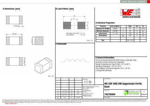
6.1 6.0 5.02012-06-262012-03-292007-02-01SStSStSKleSStSMu-Würth Elektronik eiSos GmbH & Co. KGEMC & Inductive SolutionsMax-Eyth-Str. 174638 WaldenburgGermanyTel. +49 (0) 79 42 945 - 0A Dimensions: [mm]F Typical Impedance Characteristics:Test Equipment: E4991A or equivalentF Derating Curve:H1: Classification Reflow Profile for SMT components:H2: Classification Reflow ProfilesProfile FeaturePreheat- Temperature Min (T smin ) - Temperature Max (T smax ) - Time (t s ) from (T smin to T smax )Ramp-up rate (T L to T P )Liquidous temperature (T L )Time (t L ) maintained above T L Peak package body temperature (T p )Time within 5°C of actual peak temperature (t p )Ramp-down rate (T P to T L )Time 25°C to peak temperature Pb-Free Assembly 150°C 200°C60-180 seconds 3°C/ second max.217°C60-150 seconds See Table H320-30 seconds 6°C/ second max.8 minutes max.refer to IPC/JEDEC J-STD-020DH3: Package Classification Reflow TemperaturePB-Free Assembly PB-Free Assembly PB-Free Assembly Package Thickness< 1.6 mm 1.6 - 2.5 mm ≥ 2.5 mmVolume mm³<350260°C 260°C 250°CVolume mm³350 - 2000260°C 250°C 245°CVolume mm³>2000260°C 245°C 245°Crefer to IPC/JEDEC J-STD-020DH Soldering Specifications:I Cautions and Warnings:The following conditions apply to all goods within the product series of WE-CBFof Würth Elektronik eiSos GmbH & Co. KG:General:All recommendations according to the general technical specifications of the data-sheet have to be complied with.The disposal and operation of the product within ambient conditions which probably alloy or harm the component surface has to be avoided.If the product is potted in customer applications, the potting material might shrink during and after hardening. Accordingly to this the product is exposed to the pressure of the potting material with the effect that the ferrite body and termination is possibly damaged by this pressure and so the electrical as well as the mechanical characteristics are endanger to be affected. After the potting material is cured, the ferrite body and termination of the product have to be checked if any reduced electrical or mechanical functions or destructions have occurred.The responsibility for the applicability of customer specific products and use in a particular customer design is always within the authority of the customer. All technical specifications for standard products do also apply for customer specific products.Washing varnish agent that is used during the production to clean the application might damage or change the characteristics of the plating. The washing varnish agent could have a negative effect on the long term function of the product.Direct mechanical impact to the product shall be prevented as the ferrite material of the ferrite body could flake or in the worst case it could break.Product specific:Follow all instructions mentioned in the datasheet, especially:•The solder profile has to be complied with according to the technical reflow soldering specification, otherwise no warranty will be sustai-ned.• Wave soldering is only allowed after evaluation and approval.•All products are supposed to be used before the end of the period of 12 months based on the product date-code, if not a 100% solderabi-lity can´t be warranted.•Violation of the technical product specifications such as exceeding the nominal rated current will result in the loss of warranty.1. General Customer ResponsibilitySome goods within the product range of Würth Elektronik eiSos GmbH & Co. KG contain statements regarding general suitability for certain application areas. These statements about suitability are based on our knowledge and experience of typical requirements concerning the are-as, serve as general guidance and cannot be estimated as binding statements about the suitability for a customer application. The responsibi-lity for the applicability and use in a particular customer design is always solely within the authority of the customer. Due to this fact it is up to the customer to evaluate, where appropriate to investigate and decide whether the device with the specific product characteristics described in the product specification is valid and suitable for the respective customer application or not.2. Customer Responsibility related to Specific, in particular Safety-Relevant ApplicationsIt has to be clearly pointed out that the possibility of a malfunction of electronic components or failure before the end of the usual lifetime can-not be completely eliminated in the current state of the art, even if the products are operated within the range of the specifications.In certain customer applications requiring a very high level of safety and especially in customer applications in which the malfunction or failure of an electronic component could endanger human life or health it must be ensured by most advanced technological aid of suitable design of the customer application that no injury or damage is caused to third parties in the event of malfunction or failure of an electronic component.3. Best Care and AttentionAny product-specific notes, warnings and cautions must be strictly observed.4. Customer Support for Product SpecificationsSome products within the product range may contain substances which are subject to restrictions in certain jurisdictions in order to serve spe-cific technical requirements. Necessary information is available on request. In this case the field sales engineer or the internal sales person in charge should be contacted who will be happy to support in this matter.5. Product R&DDue to constant product improvement product specifications may change from time to time. As a standard reporting procedure of the Product Change Notification (PCN) according to the JEDEC-Standard inform about minor and major changes. In case of further queries regarding the PCN, the field sales engineer or the internal sales person in charge should be contacted. The basic responsibility of the customer as per Secti-on 1 and 2 remains unaffected.6. Product Life CycleDue to technical progress and economical evaluation we also reserve the right to discontinue production and delivery of products. As a stan-dard reporting procedure of the Product Termination Notification (PTN) according to the JEDEC-Standard we will inform at an early stage about inevitable product discontinuance. According to this we cannot guarantee that all products within our product range will always be available. Therefore it needs to be verified with the field sales engineer or the internal sales person in charge about the current product availability ex-pectancy before or when the product for application design-in disposal is considered.The approach named above does not apply in the case of individual agreements deviating from the foregoing for customer-specific products.7. Property RightsAll the rights for contractual products produced by Würth Elektronik eiSos GmbH & Co. KG on the basis of ideas, development contracts as well as models or templates that are subject to copyright, patent or commercial protection supplied to the customer will remain with Würth Elektronik eiSos GmbH & Co. KG.8. General Terms and ConditionsUnless otherwise agreed in individual contracts, all orders are subject to the current version of the “General Terms and Conditions of Würth Elektronik eiSos Group”, last version available at .J Important Notes:The following conditions apply to all goods within the product range of Würth Elektronik eiSos GmbH & Co. KG:分销商库存信息: WURTH-ELECTRONICS 742792604。
DB3;DB4;SMDB3;中文规格书,Datasheet资料

October2001-Ed:2B DIACSymbol Parameter Value Unit I TRM Repetitive peak on-state currenttp=20µs F=120HzSMDB3 1.00ADB3/DB4 2.00Tstg Tj Storage temperature rangeOperating junction temperature range-40to+125°CABSOLUTE MAXIMUM RATINGS(limiting values)Note:*SMDB3indicated as Preliminary spec as product is still in development stage.1/55/5Information furnished is believed to be accurate and reliable.However,STMicroelectronics assumes no responsibility for the consequences of use of such information nor for any infringement of patents or other rights of third parties which may result from its use.No license is granted by implication or otherwise under any patent or patent rights of STMicroelectronics.Specifications mentioned in this publication are subject to change without notice.This publication supersedes and replaces all information previously supplied.STMicroelectronics products are not authorized for use as critical components in life support devices or systems without express written ap-proval of STMicroelectronics.The ST logo is a registered trademark of STMicroelectronics ©2001STMicroelectronics -Printed in Italy -All rights reserved.STMicroelectronics GROUP OF COMPANIESAustralia -Brazil -China -Finland -France -Germany -Hong Kong -India -Italy -Japan -MalaysiaMalta -Morocco -Singapore -Spain -Sweden -Switzerland -United Kingdom -U.S.A.PACKAGE MECHANICAL DATA (in millimeters)SOT-23FOOTPRINT分销商库存信息:STMDB3DB4SMDB3。