ME2804(世微)中文
合集下载
几种运算放大器型号选择

OPA342 OPA343 OPA344 OPA345 OPA347 OPA348 OPA349 OPA350 OPA353 OPA354 OPA355 OPA356 OPA357 OPA358 OPA363 OPA364 OPA365 OPA37 OPA373 OPA374 OPA379 OPA380 OPA381 OPA445 OPA452 OPA453 OPA541 OPA544
OPA547 OPA548 OPA549 OPA551 OPA552 OPA561 OPA567 OPA569 OPA602 OPA606 OPA683 OPA684 OPA690 OPA691 OPA692 OPA694 OPA703 OPA704 OPA705 OPA725 OPA726 OPA727 OPA728 OPA734 OPA735 OPA743 OPA820
精密放大器 精密放大器 精密放大器 精密放大器 精密放大器 精密放大器 精密放大器 精密放大器 精密放大器 精密放大器 高速放大器(大于等于 50MHz) 高速放大器(大于等于 50MHz) 高速放大器(大于等于 50MHz) 高速放大器(大于等于 50MHz) 视频功能 高速放大器(大于等于 50MHz) 精密放大器 精密放大器 精密放大器 精密放大器 精密放大器 精密放大器 精密放大器 精密放大器 精密放大器 精密放大器 高速放大器(大于等于 50MHz)
高速放大器(大于等于 50MHz) 高速放大器(大于等于 50MHz) 运算放大器 运算放大器 运算放大器 运算放大器 运算放大器 运算放大器 运算放大器 运算放大器 高速放大器(大于等于 50MHz) 高速放大器(大于等于 50MHz) 高速放大器(大于等于 50MHz) 高速放大器(大于等于 50MHz)
北京四方-280系列数字式保护(测控)装置说明书(0SF.451.069)_V2.0
2.7
输出触点容量............................................................................................................................ 4
2.8
装置主要技术参数.................................................................................................................... 4
3.2
装置功能组件概述.............................ห้องสมุดไป่ตู้...................................................................................... 6
3.3
交流插件(AC) ...................................................................................................................... 7
2.5
热性能(过载能力)................................................................................................................ 4
2.6
功率消耗 ................................................................................................................................... 4
MWP-T80-4的说明书
MWP-T80-4的说明书
支持热电偶、热电阻、电压、电流及二线制变送器输入;适合温度、压力、液位、长度等多种物理的测量与显示;可对各种非线性信号进行高精度的线性较正。
采用高亮度LED数码显示,同时采用高精度40线光柱显示,清晰直观。
的显示测量值。
支持多达四路报警功能,包括两路上限及两路下限报警,可独立报警
采用先进的无跳线技术,可自由更改分度号。
具有多种标准串行双向通讯功能(RS232C,RS485,RS422等)。
配智能数据采集器和基于WindowsXP平台的组态软件,可实现与上位机的联网。
面板说明
①指示灯:AHH--上上限报警
AH--上限报警AL--下限报警
ALL--下下限报警
②40段光柱:直观显示PV值的比例
③PV窗口:显示测量值,在参数设定状态下,显示参数符号或设定值
④设置键:用于进入参数设定状态,确认参数修改等
⑥数据增加键
⑦数据移位键。
SiP2804中文资料
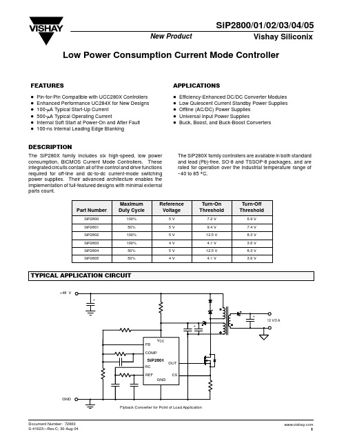
APPLICATIONS
D D D D D Efficiency-Enhanced DC/DC Converter Modules Low Quiescent Current Standby Power Supplies Offline (AC/DC) Power Supplies Universal Input Power Supplies Buck, Boost, and Buck-Boost Converters
100% 50% 100% 100% 50% 50%
The SiP280X family controllers are available in both standard and lead (Pb)-free, SO-8 and TSSOP-8 packages, and are rated for operation over the industrial temperature range of --40 to 85 _C.
2
Document Number: 72660 S-41623—Rev.C, 30-Aug-04
元器件交易网
SiP2800/01/02/03/04/05
New Product
SPECIFICATIONS
Test Conditions Unless Specified Parameter
New Product
Currents are positive into, negative out of the specificed terminal.
Stresses beyond those listed under “Absolute Maximum Ratings” may cause permanent damage to the device. These are stress ratings only, and functional operation of the device at these or any other conditions beyond those indicated in the operational sections of the specifications is not implied. Exposure to absolute maximum rating conditions for extended periods may affect device reliability.
ME2804最新中文版(2014版)

VIN (V)
3、DETECT, RELEASE VOLTAGE VS. AMBIENT TEMPERATURE
4、N-ch OUTPUT CURRENT VS. INPUT VOLTAGE
VDS=0.5V -VDET=1.1V -VDET=1.1V
VDET VS TEMP 1.25 1.2 1.15 1.1 1.05 1 -15 7 20 30 40 50 60 70 80 90 100 110 120 TEMP (℃ )
Max.
-VDET(S) ×1.02 -VDET(S) ×1.01 0.1 1 1 2 2 2 --
Units
-VDET -VDET(S)>2.2V VHYS VIN=2V (1.0V-1.5V)
V
V
VIN =3.5V (1.6V-2.5V) Supply Current ISS VIN=4.5V (2.6V-3.9V) VIN =6V VIN=7V Output Current Operating voltage Responding time Temperature characteristics Iout N-ch VIN
Functional Description:
1、 When input voltage (VIN) rises above detect voltage (–VDET), output voltage (VOUT) will be equal to VIN. 2、 When input voltage (VIN) falls below detect voltage (–VDET), output voltage (VOUT) will be equal to the ground voltage (VSS) level. 3、 When input voltage (VIN) falls to a level below that of the minimum operating voltage (VMIN), output will become unstable. In this condition, V IN will equal the pulled-up output (should output be pulled-up.) 4、 When input voltage (VIN) rises above the ground voltage (VSS) level, output will be unstable at levels below the minimum operating voltage (VMIN). Between the VMIN and detect release voltage (+VDET) levels, the ground voltage (VSS) level will be maintained. 5、 When input voltage (VIN) rises above detect release voltage (+VDET), output voltage (VOUT) will be equal to VIN. 6、 The difference between +VDET and –VDET represents the hysteresis range.
PAM2804-Rev1.0

PAM2804
1A Step-Down Constant Current, High Efficiency LED Driver
Features
Efficiency up to 93% n n 180 μ A(TYP.) Quiescent Current n Output Current: Up to 1A n Internal Synchronous Rectifier n 1.5MHz Switching Frequency n Soft Start n Under-Voltage Lockout n Short LED Protection n Open LED Protection n Thermal Shutdown n 5-pin Small SOT23-5 Packages n Pb-Free Package
Power Analog Microelectronics , Inc
10/2010 Rev1.0
2
PAM2804
1A Step-Down Constant Current, High Efficiency LED Driver
Absolute Maximum Ratings
T A=25 °C , V IN=4.2V, Real WLED load, C IN=10µF, C O=10µF, L=4.7µH, unless otherwise noted.
PARAMETER Input Voltage Range Regulated Feedback Voltage Peak Inductor Current Quiescent Current Shutdown Current Oscillator Frequency Drain-Source On-State Resistance SW Leakage Current High Efficiency EN Threshold High EN Threshold Low EN Leakage Current Over Temperature Protection OTP Hysteresis SYMBOL VIN V FB IPK IQ ISD fOSC RDS(O N) ILSW η VEH VEL IEN OTP OTH ±0.01 150 30 1.5 0.3 VIN=5V No load VEN = 0V VO = 100% IDS=100mA P MOSFET N MOSFET 1.2 1.5 0.3 0.35 ±0.01 93 Test Conditions MIN 2.5 0.095 0.1 1.5 180 1 1.8 0.45 0.5 1 TYP MAX 6.0 0.105 UNITS V V A µA µA MHz Ω Ω µA % V V µA °C °C
1A Step-Down Constant Current, High Efficiency LED Driver
Features
Efficiency up to 93% n n 180 μ A(TYP.) Quiescent Current n Output Current: Up to 1A n Internal Synchronous Rectifier n 1.5MHz Switching Frequency n Soft Start n Under-Voltage Lockout n Short LED Protection n Open LED Protection n Thermal Shutdown n 5-pin Small SOT23-5 Packages n Pb-Free Package
Power Analog Microelectronics , Inc
10/2010 Rev1.0
2
PAM2804
1A Step-Down Constant Current, High Efficiency LED Driver
Absolute Maximum Ratings
T A=25 °C , V IN=4.2V, Real WLED load, C IN=10µF, C O=10µF, L=4.7µH, unless otherwise noted.
PARAMETER Input Voltage Range Regulated Feedback Voltage Peak Inductor Current Quiescent Current Shutdown Current Oscillator Frequency Drain-Source On-State Resistance SW Leakage Current High Efficiency EN Threshold High EN Threshold Low EN Leakage Current Over Temperature Protection OTP Hysteresis SYMBOL VIN V FB IPK IQ ISD fOSC RDS(O N) ILSW η VEH VEL IEN OTP OTH ±0.01 150 30 1.5 0.3 VIN=5V No load VEN = 0V VO = 100% IDS=100mA P MOSFET N MOSFET 1.2 1.5 0.3 0.35 ±0.01 93 Test Conditions MIN 2.5 0.095 0.1 1.5 180 1 1.8 0.45 0.5 1 TYP MAX 6.0 0.105 UNITS V V A µA µA MHz Ω Ω µA % V V µA °C °C
SL2804数据手册

In MillimeterDsimensions
Min
Max
1.400
1.600
0.320
0.520
0.400
0.580
0.350
0.440
4.400
4.600
1.550 REF
2.300
2.600
3.940
4.250
1.500 TYP
3.000 TYP
0.900
1.200
Dimensions In Inches
Min
Max
0.055
0.063
0.013
0.197
0.016
0.023
0.014
0.017
0.173
0.181
0.061 REF
0.091
0.102
0.155
0.167
0.060TYP
0.118TYP
0.035
0.047
7 of 7
特性:
最高效率:95% 最高工作频率:300KHz 低静态电流:15uA 输出电压:2.5V~5.0V(步进 0.1V) 输出精度:±2.5% 输入电压:0.9V~5.0V 低纹波,低噪声
管脚功能:
SL2804
SL2804
SL2804 SL2804
VOUT 3
SL2804 (SOT-23-3)
1
2
GND
5.0
V
0.8
V
V
%
90
94
%
800
1000
mA
15
uA
L
VIN Cin +-
47uH 100uF
VOUT
LX
P2804ND5G中文资料

1 2
N-Ch P-Ch N-Ch P-Ch N-Ch P-Ch 42 55 30 52
1.2 -1.2
V
nS
Qrr
nC
Pulse test : Pulse Width ≤ 300 µsec, Duty Cycle ≤ 2%. Independent of operating temperature. 3 Pulse width limited by maximum junction temperature. REMARK: THE PRODUCT MARKED WITH “P2804ND5G”, DATE CODE or LOT # Orders for parts with Lead-Free plating can be placed using the PXXXXXXG parts name.
790 690 175 310 65 75 16 14 2.5 2.2 2.1 1.9
988 863 245 430 98 113 pF
Output Capacitance
Coss
Reverse Transfer Capacitance Total Gate Charge2 Gate-Source Charge2 Gate-Drain Charge2
TO-252-5 (DPAK) MECHANICAL DATA
mm Dimension Min. A B C D E F G 9.0 2.1 0.4 1.1 0.4 0.00 5.3 5.5 Typ. 9.5 2.3 0.5 1.2 0.5 Max. 10.0 2.5 0.6 1.3 0.6 0.3 5.7 H I J K L M N Dimension Min. 1.3 6.3 4.8 0.8 0.3 1.1 Typ. 1.5 6.5 5.0 1.3 0.5 1.3 Max. 1.7 6.7 5.2 1.8 0.7 1.5 mm
- 1、下载文档前请自行甄别文档内容的完整性,平台不提供额外的编辑、内容补充、找答案等附加服务。
- 2、"仅部分预览"的文档,不可在线预览部分如存在完整性等问题,可反馈申请退款(可完整预览的文档不适用该条件!)。
- 3、如文档侵犯您的权益,请联系客服反馈,我们会尽快为您处理(人工客服工作时间:9:00-18:30)。
Inches Max 0.0630 0.0630 0.0189 0.0209 0.0189 0.0689 0.0169 0.0630 0.181 0.1673 0.1023 -
13620971652
Page 6 of 9
ME2804
·SOT-23-3
Millimeters DIM Min A B b C c d E e 2.7 1.7 0.35 1.0 0.1 0.2 2.6 1.5 Max 3.1 2.1 0.5 1.2 0.25 3.0 1.8 Min 0.1063 0.0669 0.0138 0.0394 0.0039 0.0079 0.1023 0.059
Min 0.13386 0.0118 0.1732 0.1732 0.0354 0.046 0.094 0.4724
Max 0.1496 0.0197 0.189 0.189 0.059 0.0539 0.1059 0.6299
Typical Application Circuit
13620971652
Page 1 of 9
ME2804
Pin Configuration
TO-92
SOT-23-3
SOT-89-3
Pin Assignment
ME2804XX Pin Number SOT-23-3 SOT-89-3 TO-92 Pin Name Functions
Iss VS Temp 1 0.9 0.8 0.7 0.6 0.5 0.4 0.3 0.2 -15 7 20 30 40 50 60 70 80 90 100 Temp (℃ )
1.6 1.4 1.2
Iss (uA)
Iss VS VIN
Iss (uA)
1 0.8 0.6 0.4 0.2 0 0.5 1 1.5 2 2.5 3 3.5 4 4.5 5 5.5 6
ME2804
Voltage Detectors , ME2804 Series
General Description
ME2804 Series are highly precise, low power consumption voltage detectors, manufactured using NMOS technologies. Detect voltage is extremely accurate with minimal temperature drift. NMOS output configurations are available. Operating voltage range:0.7V~7V Detect voltage temperature characteristics: TYP± 100ppm/℃ Output configuration:NMOS Package: SOT-23-3,SOT-89-3,TO-92
Inches Max 0.122 0.0827 0.0197 0.0472 0.0098 0.1181 0.0708
13620971652
Page 7 of 9
ME2804
·TO-92
Min A B C D E e e1 L 3.4 0.3 4.4 4.4 0.9 1.17 2.39 12
Max 3.8 0.5 4.8 4.8 1.5 1.37 2.69 16
Features
Highly accuracy: ± 1% (-VDET=2.2V 以上) Low power consumption: TYP 0.7uA (VIN=3.5V, -VDET=2.2V) Detect voltage range: 1.0V~6.5V in 0.1V increments
13620971652
Page 4 of 9
ME2804
Type Characteristics
1、SUPPLY CURRENT VS. AMBIENT TEMPERATURE VIN=2V,-VDET=1.1V 2、SUPPLY CURRENT VS. INPUT VOLTAGE -VDET=1.1V (T=25℃)
Functional Description:
1、 When input voltage (VIN) rises above detect voltage (–VDET), output voltage (VOUT) will be equal to VIN. 2、 When input voltage (VIN) falls below detect voltage (–VDET), output voltage (VOUT) will be equal to the ground voltage (VSS) level. 3、 When input voltage (VIN) falls to a level below that of the minimum operating voltage (VMIN), output will become unstable. In this condition, V IN will equal the pulled-up output (should output be pulled-up.) 4、 When input voltage (VIN) rises above the ground voltage (VSS) level, output will be unstable at levels below the minimum operating voltage (VMIN). Between the VMIN and detect release voltage (+VDET) levels, the ground voltage (VSS) level will be maintained. 5、 When input voltage (VIN) rises above detect release voltage (+VDET), output voltage (VOUT) will be equal to VIN. 6、 The difference between +VDET and –VDET represents the hysteresis range.
VIN (V)
3、DETECT, RELEASE VOLTAGE VS. AMBIENT TEMPERATURE
4、N-ch OUTPUT CURRENT VS. INPUT VOLTAGE
VDS=0.5V -VDET=1.1V -VDET=1.1V
VDET VS TEMP 1.25 1.2 1.15 1.1 1.05 1 -15 7 20 30 40 50 60 70 80 90 100 110 120 TEMP (℃ )
Selection Guide
Typical Application
Microprocessor reset circuitry Memory battery back-up circuits Power-on reset circuits Power failure detection System battery life and charge voltage monitors
2 1 3
3 1 2
3 1 2
VSS VOUT VIN
Ground Output Voltage Input Voltage
Block Diagram
Absolute Maximum Ratings
PARAMETER VIN Input Voltage Output Current Output Voltage Continuous Total Power Dissipation CMOS SOT-23-3 SOT-89-3 TO-92 TOpr Tstg Tsolder MM HBM Pd SYMBAL VIN IOUT VOUT RATINGS 8 50 VSS-0.3~VIN+0.3 300 500 500 -40~+85 -40~+125 260℃, 10s 400 4000 V V ℃ ℃ mW UNITS V mA V
Operating Ambient Temperature Storage Temperature Soldering temperature and time ESD
13620971652
Page 2 of 9
ME2804
Electrical Characteristics
(-VDET(S)=1.0V to 6.5V ,Ta=25OC ,unless otherwise noted)
tpLH
uA
(4.0V-5.6V) (5.7V-6.5V) 0.01
VDS=0.5V VIN =0.7V
0.14
mA
-
0.7
-
7 60
V us ppm/℃
VDET Ta VDET
Ta =-40℃ ~ 85℃
-
± 100
± 350
Note: 1、-VDET(S) :Specified Detection Voltage value 2、-VDET :Actual Detection Voltage value 3、Release Voltage:+VDET=-VDET+VHYS
13620971652
Page 3 of 9
ME2804
Timing Chart:
ME2804AXX:
Directions for use:
Notes on Use 1、 Please use this IC within the stated maximum ratings. Operation beyond these limits may cause degrading or permanent damage to the device. 2、In order to stabilize the IC’s operations, please ensure that VIN pin’s input frequency’s rise and fall times are more than several u Sec/V.