NADCA-E10-83 - Flash Removal(2015-11-26)
分项报价表

分项报价表采购编号:YJGPC2022045Z项目名称:文物保护科研设备采购项目包号:1投标人名称:西安鼎诺测控技术有限公司货币及单位:人民币/元1品目号序号货物名称规格型号品牌产地制造商名称单价数量总价1-11扫描电子显微镜配套能谱仪Prisma E赛默飞捷克T h e r m o F i s h e r S c i e n t i f i c B r n o s.r .o .2,693,000.001.00 (套)2,693,000.001-21高性能微区X 射线荧光成像光谱仪M4 Tornado 布鲁克德国B r u k er N a n o G m b H2,172,000.001.00 (套)2,172,000.001-22高性能光纤拉曼光谱仪Virsa 雷尼绍英国Renish aw plc 1,989,000.001.00 (套)1,989,000.001-23离子色谱仪ICS 6000赛默飞墨西哥T h e r m o s c i e n t i f i c1,481,000.001.00 (套)1,481,000.001-24扫描电子显微镜室制样间改造KFR-35GW/NhG c1B 等格力等中国珠海等珠海格力电器股份有限公司等21,500.001.00 (处)21,500.00投标人盖章:日期:2022 年 11 月 14 日广东政府采购智慧云平台YJ GP C 2022045Z第(1) 采购包 2022-11-14 18:28:1西安鼎诺测控技术有限公司2022-11-1418:28:10。
ADN8810 12位高输出电流源数据手册(版本C)说明书
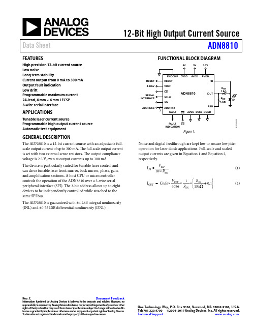
12-Bit High Output Current Source Data Sheet ADN8810Rev. C Document FeedbackInformation furnished by Analog Devices is believed to be accurate and reliable. However, noresponsibility is assumed by Analog Devices for its use, nor for any infringements of patents or other rights of third parties that may result from its use. Specifications subject to change without notice. No license is granted by implication or otherwise under any patent or patent rights of Analog Devices. T rademarks and registered trademarks are the property of their respective owners. O ne Technology Way, P.O. Box 9106, Norwood, MA 02062-9106, U.S.A. Tel: 781.329.4700 ©2004–2017 Analog Devices, Inc. All rights reserved. Technical Support FEATURESHigh precision 12-bit current sourceLow noiseLong term stabilityCurrent output from 0 mA to 300 mA Output fault indicationLow driftProgrammable maximum current24-lead, 4 mm × 4 mm LFCSP3-wire serial interface APPLICATIONSTunable laser current source Programmable high output current source Automatic test equipmentFUNCTIONAL BLOCK DIAGRAM3195-0 RESET4.096VSERIALINTERF ACEADDRESSSBF AULTINDICA TIONFigure 1.GENERAL DESCRIPTIONThe ADN8810 is a 12-bit current source with an adjustable full-scale output current of up to 300 mA. The full-scale output current is set with two external sense resistors. The output compliance voltage is 2.5 V, even at output currents up to 300 mA.The device is particularly suited for tunable laser control and can drive tunable laser front mirror, back mirror, phase, gain, and amplification sections. A host CPU or microcontroller controls the operation of the ADN8810 over a 3-wire serial peripheral interface (SPI). The 3-bit address allows up to eight devices to be independently controlled while attached to the same SPI bus.The ADN8810 is guaranteed with ±4 LSB integral nonlinearity (INL) and ±0.75 LSB differential nonlinearity (DNL). Noise and digital feedthrough are kept low to ensure low jitteroperation for laser diode applications. Full-scale and scaledoutput currents are given in Equation 1 and Equation 2,respectively.SNREFFS RVI⨯≈10(1)⎪⎪⎪⎪⎭⎫⎝⎛+Ω⨯⨯⨯=1.01514096kRRVCodeI SNSNREFOUT(2)ADN8810Data SheetRev. C | Page 2 of 14TABLE OF CONTENTSFeatures .............................................................................................. 1 Applications ....................................................................................... 1 Functional Block Diagram .............................................................. 1 General Description ......................................................................... 1 Revision History ............................................................................... 2 Specifications ..................................................................................... 3 Timing Characteristics ................................................................ 4 Absolute Maximum Ratings ............................................................ 5 ESD Caution .................................................................................. 5 Pin Configuration and Function Descriptions ............................. 6 Typical Performance Characteristics ............................................. 7 Terminology ...................................................................................... 9 Functional Description (10)Setting Full-Scale Output Current ........................................... 10 Power Supplies ............................................................................ 10 Serial Data Interface ................................................................... 10 Standby and Reset Modes ......................................................... 11 Power Dissipation....................................................................... 11 Using Multiple ADN8810 Devices for Additional Output Current ......................................................................................... 11 Adding Dither to the Output Current ..................................... 12 Driving Common-Anode Laser Diodes ................................. 12 PCB Layout Recommendations ............................................... 13 Suggested Pad Layout for CP-24 Package ............................... 13 Outline Dimensions ....................................................................... 14 Ordering Guide .. (14)REVISION HISTORY11/2017—Rev. B. to Rev. CChanged R S to R SN .......................................................... Throughout Change to Figure 1 ........................................................................... 1 Changes to Maximum Full-Scale Output Current Parameter and Power Supply Rejection Ratio Parameter, Table 1 ................ 3 Moved Timing Characteristics Section, Table 2, and Figure 2 ..... 4 Added Lead Temperature Range (Soldering 10 sec) Parameter, Table 3 ................................................................................................ 5 Changes to Figure 3 and Table 4 ..................................................... 6 Changes to Setting Full-Scale Output Current Section ............. 10 Changes to Adding Dither to the Output Current Section,Figure 20, and Figure 21 ................................................................ 12 Changes to PCB Layout Recommendations Section andFigure 25 .......................................................................................... 13 Updated to Outline Dimensions .................................................. 14 3/2016—Rev. A to Rev. BChanges to Figure 3 and Table 4 ...................................................... 7 Updated Outline Dimensions ....................................................... 15 Changes to Ordering Guide . (15)4/2009—Rev. 0 to Rev. A Changes to Table 3 ............................................................................. 6 Changes to Figure 25 ...................................................................... 14 Updated Outline Dimensions ....................................................... 15 Changes to Ordering Guide . (15)1/2004—Revision 0: Initial VersionData Sheet ADN8810 SPECIFICATIONSAVDD = DVDD = 5 V, PVDD = 3.3 V, AVSS = DVSS = DGND = 0 V, T A = 25°C, covering output current (I OUT) from 2% full-scale current (I FS) to 100% I FS, unless otherwise noted.Rev. C | Page 3 of 14ADN8810Data SheetRev. C | Page 4 of 141 With respect to AVSS. 2R SN = 20 Ω. 3See Table 2 for timing specifications.TIMING CHARACTERISTICS1, 21 Guaranteed by design. Not production tested.2Sample tested during initial release and after any redesign or process change that may affect these parameters. All input signals are measured with tr = tf = 5 ns (10% to 90% of DVDD) and timed from a voltage level of (V IL + V IH )/2.SCLKC SSDIRESET*ADDRESS BIT A3 MUST BE LOGIC LOW03195-0-002Figure 2. Timing DiagramData SheetADN8810Rev. C | Page 5 of 14ABSOLUTE MAXIMUM RATINGSTable 3.Parameter Rating Supply Voltage 6 VInput VoltageGND to V S + 0.3 V Output Short-Circuit Duration to GND IndefiniteStorage Temperature Range −65°C to +150°C Operating Temperature Range−40°C to +85°C Junction Temperature Range, CP Package −65°C to +150°C Lead Temperature Range (Soldering 10 sec)300°CStresses at or above those listed under Absolute Maximum Ratings may cause permanent damage to the product. This is a stress rating only; functional operation of the product at these or any other conditions above those indicated in the operational section of this specification is not implied. Operation beyond the maximum operating conditions for extended periods may affect product reliability.ESD CAUTIONADN8810Data SheetRev. C | Page 6 of 14PIN CONFIGURATION AND FUNCTION DESCRIPTIONS03195-0-003FAULT ADDR0ADDR1FB RSN ADDR2NICVREF AVDD AVSS NIC DVSS117P V D D I O U T I O U T P V D D 1E N C O M P S B NOTES1. NIC = NOT INTERNALLY CONNECTED.2. EXPOSED PAD. CONNECT THE EXPOSED PAD TO DGND.Figure 3. Pin ConfigurationData SheetADN8810Rev. C | Page 7 of 14TYPICAL PERFORMANCE CHARACTERISTICSCODE1.2–0.84,500500I N L E R R O R (L S B )1,0001,5002,0002,5003,0003,5004,0001.00.2–0.2–0.4–0.60.80.600.403195-0-005Figure 4. Typical INL PlotCODE0.4–0.304,500500D N LE R R O R (L S B )1,0001,5002,0002,5003,0003,5004,0000.1–0.1–0.20.300.203195-0-006Figure 5. Typical DNL PlotTEMPERATURE (°C)0.200.15–0.20–4085–15∆I N L (L S B )1035600–0.05–0.10–0.150.100.0503195-0-007Figure 6. ∆INL vs. TemperatureTEMPERATURE (°C)0.200.15–0.20–4085–15∆D N L (L S B )1035600–0.05–0.10–0.150.100.0503195-0-008Figure 7. ∆DNL vs. TemperatureTEMPERATURE (°C)0.2580.2570.250–4085–15F U L L -S C A L E O U T P U T (A )1035600.2540.2530.2520.2510.2560.255R SN = 1.6Ω03195-0-009Figure 8. Full-Scale Output vs. TemperatureTEMPERATURE (°C)20.76520.75520.720–4085–15F U L L -S C A L E O U T P U T (m A )10356020.74020.73520.73020.72520.75020.745R SN = 20Ω20.76003195-0-010Figure 9. Full-Scale Output vs. TemperatureADN8810Data SheetRev. C | Page 8 of 14TEMPERATURE (°C)0.500.35I P V D D (m A )0.200.150.100.050.300.250.400.4503195-0-011Figure 10. PVDD Supply Current (I PVDD ) vs. Temperature120I D V D D (µA )864210TEMPERATURE (°C)03195-0-012Figure 11. DVDD Supply Current (I DVDD ) vs. Temperature1.51.0I A V D D (m A )1.41.31.21.1TEMPERATURE (°C)03195-0-013Figure 12. AVDD Supply Current (I AVDD ) vs. TemperatureFREQUENCY (Hz)100k1O U T P U T I M P E D A N C E (Ω)1k1001010k03195-0-014Figure 13. Output Impedance vs. FrequencyTIME (1µs/DIV)CSI OUTV O L T A GE (2.7V /D I V )03195-0-015Figure 14. Full-Scale Settling TimeTIME (200ns/DIV)CSI OUT03195-0-016Figure 15. 1 LSB Settling TimeData SheetADN8810Rev. C | Page 9 of 14TERMINOLOGYRelative AccuracyRelative accuracy or integral nonlinearity (INL) is a measure of the maximum deviation, in least significant bits (LSBs), from an ideal line passing through the endpoints of the DAC transfer function. Figure 4 shows a typical INL vs. code plot. The ADN8810 INL is measured from 2% to 100% of the full-scale (FS) output.Differential NonlinearityDifferential nonlinearity (DNL) is the difference between the measured change and the ideal 1 LSB change between any two adjacent codes. A specified differential nonlinearity of ± 1 LSB maximum ensures monotonicity. The ADN8810 is guaranteed monotonic by design. Figure 5 shows a typical DNL vs. code plot . Offset ErrorOffset error, or zero-code error, is an interpolation of the output voltage at code 0x000 as predicted by the line formed from the output voltages at code 0x040 (2% FS) and code 0xFFF (100% FS). Ideally, the offset error is 0 V . Offset error occurs from a combination of the offset voltage of the amplifier and offset errors in the DAC. It is expressed in LSBs.Offset DriftThis is a measure of the change in offset error with a change in temperature. It is expressed in (ppm of full-scale range)/°C. Gain ErrorGain error is a measure of the span error of the DAC. It is the deviation in slope of the output transfer characteristic from ideal. The transfer characteristic is the line formed from the output voltages at code 0x040 (2% FS) and code 0xFFF (100% FS). It is expressed as a percent of the full-scale range.Compliance VoltageThe maximum output voltage from the ADN8810 is a function of output current and supply voltage. Compliance voltage defines the maximum output voltage at a given current and supply voltage to guarantee the device operates within its INL, DNL, and gain error specifications.Output Current Change vs. Output Voltage ChangeThis is a measure of the ADN8810 output impedance and is similar to a load regulation spec in voltage references. For a given code, the output current changes slightly as output voltage increases. It is measured as an absolute value in (ppm of full-scale range)/V .O U T P U T V O L T A G E03195-0-004Figure 16. Output Transfer FunctionADN8810Data SheetRev. C | Page 10 of 14FUNCTIONAL DESCRIPTIONThe ADN8810 is a single 12-bit current output digital-to-analog converter (DAC) with a 3-wire SPI interface. Up to eight devices can be independently programmed from the same SPI bus. The full-scale output current is set with two external resistors. The maximum output current can reach 300 mA. Figure 17 shows the functional block diagram of the ADN8810.03195-0-017Figure 17. Functional Blocks, Pins, and Internal ConnectionsSETTING FULL-SCALE OUTPUT CURRENTTwo external resistors set the full-scale output current from the ADN8810. These resistors are equal in value and are labeled R SN in Figure 1. Use 1% or better tolerance resistors to achieve the most accurate output current and the highest output impedance.Equation 3 shows the approximate full-scale output current. The exact output current is determined by the data register code as shown in Equation 4. The variable code is an integer from 0 to 4095, representing the full 12-bit range of the ADN8810.SNFS R I ×≈10096.4(3)+Ω××=1.0151000,1k R R Code I SN SN OUT(4)The ADN8810 is designed to operate with a 4.096 V referencevoltage connected to VREF. The output current is directly proportional to this reference voltage. To achieve the bestperformance, use a low noise precision (the ADR292, ADR392, or REF198 is recommended).POWER SUPPLIESThere are three principal supply current paths through the ADN8810: •AVDD provides power to the analog front end of the ADN8810 including the DAC. Use this supply line topower the external voltage reference. For best performance, AVDD must be low noise.•DVDD provides power for the digital circuitry. Thisincludes the serial interface logic, the SB and RESET logic inputs, and the FAULT output. Tie DVDD to the same supply line used for other digital circuitry. It is not necessary for DVDD to be low noise.•PVDD is the power pin for the output amplifier. It canoperate from as low as 3.0 V to minimize power dissipation in the ADN8810. For best performance, PVDD must be low noise.Current is returned through the following three pins: •AVSS is the return path for both AVDD and PVDD. This pin is connected to the substrate of the die as well as the slug on the bottom of the lead frame chip scale package (LFCSP). For single-supply operation, connect this pin to a low noise ground plane.•DVSS returns current from the digital circuitry powered by DVDD. Connect DVSS to the same ground line or plane used for other digital devices in the application.•DGND is the ground reference for the digital circuitry. In a single-supply application, connect DGND to DVSS.For single-supply operation, set AVDD to 5 V , set PVDD from 3.0 V to 5 V , and connect AVSS, AGND, and DGND to ground.SERIAL DATA INTERFACEThe ADN8810 uses a serial peripheral interface (SPI) with three input signals: SDI, CLK, and CS . Figure 2 shows the timing diagram for these signals.Data applied to the SDI pin is clocked into the input shift register on the rising edge of CLK. After all 16 bits of the data-word have been clocked into the input shift register, a logic high on CS loads the shift register byte into the ADN8810. If more than 16 bits of data are clocked into the shift register before CS goes high, bits are pushed out of the register in first-in first-out (FIFO) fashion.The four MSB of the data byte are checked against the address of the device. If they match, the next 12 bits of the data byte are loaded into the DAC to set the output current. The first bit (MSB) of the data byte must be a logic zero, and the following three bits must correspond to the logic levels on pins ADDR2, ADDR1, and ADDR0, respectively, for the DAC to be updated. Up to eight ADN8810 devices with unique addresses can be driven from the same serial data bus.Table 5 shows how the 16-bit DATA input word is divided into an address byte and a data byte. The first four bits in the input word correspond to the address. Note that the first bit loaded (A3) must always be zero. The remaining bits set the 12-bit data byte for the DAC output. Three example inputs are demonstrated.•Example 1: This SDI input sets the device with an address of 111 to its minimum output current, 0 A. Connecting the ADN8810 pins ADDR2, ADDR1, and ADDR0 to VDD sets this address.• Example 2: This input sets the device with an address of 000 to a current equal to half of the full-scale output. •Example 3: The ADN8810 with an address of 100 is set to full-scale output.STANDBY AND RESET MODESApplying a logic low to the SB pin deactivates the ADN8810 and puts the output into a high impedance state. The device continues to draw 1.3 mA of typical supply current in standby. When logic high is reasserted on the SB pin, the output current returns to its previous value within 6 µs.Applying logic low to RESET sets the ADN8810 data register to all zeros, bringing the output current to 0 A. When RESET is deasserted, the data register can be reloaded. Data cannot be loaded into the device while it is in standby or reset mode.POWER DISSIPATIONThe power dissipation of the ADN8810 is equal to the output current multiplied by the voltage drop from PVDD to the output.()SN OUT OUT OUT DISS R I V PVDD I P ×−−×=²(5)The power dissipated by the ADN8810 causes a temperature increase in the device. For this reason, PVDD must be as low as possible to minimize power dissipation.While in operation, the ADN8810 die temperature, also known as junction temperature, must remain below 150°C to prevent damage. The junction temperature is approximatelyDISS JA A J P T T ×θ+=(6)where:T A is the ambient temperature in °C,θJA is the thermal resistance of the package (32°C/W). •Example 4: A 300 mA full-scale output current is required to drive a laser diode within an 85°C environment. The laser diode has a 2 V drop and PVDD is 3.3 V .Using Equation 5, the power dissipation in the ADN8810 is found to be 267 mW . At T A = 85°C, this makes the junction temperature 93.5°C, which is well below the 150°C limit. Note that even with PVDD set to 5 V , the junction temperature increases to only 110°C.USING MULTIPLE ADN8810 DEVICES FOR ADDITIONAL OUTPUT CURRENTConnect multiple ADN8810 devices in parallel to increase the available output current. Each device can deliver up to 300 mA of current. To program all parallel devices simultaneously, set all device addresses to the same address byte and drive all CS , SDI, and CLK from the same serial data interface bus. The circuit in Figure 18 uses two ADN8810 devices and delivers 600 mA to the pump laser.SERIAL INTERFACE (FROM µC OR DSP)I 600mA03195-0-018Figure 18. Using Multiple Devices for Additional Output CurrentTable 5. Serial Data Input ExamplesAddress Byte Data Byte SDI Input A3 A2 A1 A0D11 D10 D9 D8 D7 D6 D5 D4D3 D2 D1 D0 Example 1 0 1 1 1 0 0 0 0 0 0 0 0 0 0 0 0 Example 2 0 0 0 0 1 0 0 0 0 0 0 0 0 0 0 0 Example 31 01111 11 11 1 1 1 1ADDING DITHER TO THE OUTPUT CURRENTSome tunable laser applications require the laser diode bias current to be modulated or dithered. This is accomplished by dithering the V REF voltage input to the ADN8810. Figure 19 demonstrates one method.DITHERR203195-0-019Figure 19. Adding Dither to the Reference VoltageSet the gain of the dither by adjusting the ratio of R2 to R1. Increase C to lower the cutoff frequency of the high-pass filter created by C and R1. The cutoff frequency of Figure 19 is approximately 98 Hz.The AD8605 is recommended as a low offset, rail-to-rail input amplifier for this circuit.DRIVING COMMON-ANODE LASER DIODESThe ADN8810 can power common-anode laser diodes. These are laser diodes whose anodes are fixed to the laser module case. The module case is typically tied to either VDD or ground. For common anode to ground applications, a −5 V supply must be provided.In Figure 20, R SN sets up the diode current by the following equation:40965.16111.1096.4Code k R I SN ×Ω+×=(7)where Code is an integer value from 0 to 4095.Using the values in Figure 20, the diode current is 300.7 mA at a code value of 2045 (0x7FF), or half full-scale. This effectively provides 11-bit current control from 0 mA to 300 mA of diode current.The maximum output current of this configuration is limited by the compliance voltage at the IOUT pin of the ADN8810. The voltage at IOUT cannot exceed 1 V below PVDD, in this case, 4 V. The IOUT voltage is equal to the voltage drop across R S N plus the gate-to-source voltage of the external FET. For this reason, select a FET with a low threshold voltage.In addition, the voltage across the R SN resistor cannot exceed the voltage at the cathode of the laser diode. Given a forward laser diode voltage drop of 2 V in Figure 20, the voltage at the RSN pin (I × R SN ) cannot exceed 3 V . This sets an upper limit to the value of code in Equation 5.Although the configuration for anode-to-ground diodes is similar, the supply voltages must be shifted down to 0 V and −5 V , as shown in Figure 21. The AVDD, DVDD, and PVDD pins are connected to ground with AVSS connected to −5 V .The 4.096 V reference must also be referred to the −5 V supply voltage. The diode current is still determined by Equation 7. All logic levels must be shifted down to 0 V and −5 V levels as well. This includes RESET , CS , SCLK, SDI, SB , and all ADDR pins. Figure 22 shows a simple method to level shift a standard TTL or CMOS (0 V to 5 V) signal down using external FETs.NOTE: LEAVE FB WITH NO CONNECTION03195-0-020Figure 20. Driving Common-Anode-to-VDD Laser DiodesNOTE: LEAVE FB WITH NO CONNECTION03195-0-021Figure 21. Driving Common-Anode-to-Ground Laser Diodes with a NegativeSupplyRESETCS SCLK SDI03195-0-022Figure 22. Level Shifting TTL/CMOS LogicPCB LAYOUT RECOMMENDATIONSAlthough they can be driven from the same power supply voltage, keep DVDD and AVDD current paths separate on the printed circuit board (PCB) to maintain the highest accuracy; likewise for AVSS and DGND. Tie common potentials together at a single point located near the power regulator. This technique is known as star grounding and is shown in Figure 23. This method reduces digital crosstalk into the laser diode or load.LOGIC GROUNDRETURN03195-0-023Figure 23. Star Supply and Ground TechniqueTo improve thermal dissipation, solder the slug on the bottom of the LFCSP package be soldered to the PCB with multiple vias into a low noise ground plane. Connecting these vias to a copper area on the bottom side of the board further improves thermal dissipation.Use identical trace width and lengths for the two output sense resistors. These lengths are shown as X and Y in Figure 24. Differences in trace lengths cause differences in parasitic seriesresistance. Because the sense resistors can be as low as 1.37 Ω, small parasitic differences can lower both the output current accuracy and the output impedance. See the AN-619 Application Note for a sample layout for these traces.03195-0-024Figure 24. Use Identical Trace Lengths for Sense ResistorsSUGGESTED PAD LAYOUT FOR CP-24 PACKAGEFigure 25 shows the dimensions for the PCB pad layout for the ADN8810. The package is a 4 mm × 4 mm, 24-lead LFCSP . The metallic slug underneath the package must be soldered to a copper pad connected to AVSS, the lowest supply voltage to the ADN8810. For single-supply applications, this is ground. Use multiple vias to this pad to improve the thermal dissipation of the package.0.0270.011(0.28)0.020(0.50)CONTROLLING DIMENSIONS ARE IN MILLIMETERS03195-0-025Figure 25. Suggested PCB Layout for the CP-24-10 Pad LandingOUTLINE DIMENSIONS0.300.250.200.800.750.700.25 MIN2.202.10 SQ 2.000.50BSC0.500.400.30COMPLIANT TO JEDEC STANDARDS MO-220-WGGD-8.BOTTOM VIEWTOP VIEWSIDE VIEW4.104.00 SQ 3.900.05 MAX 0.02 NOM0.203 REFCOPLANARITY0.08PIN 1INDICATORFOR PROPER CONNECTION OF THE EXPOSED PAD, REFER TO THE PIN CONFIGURATION AND FUNCTION DESCRIPTIONSSECTION OF THIS DATA SHEET.02-21-2017-AEXPOSED PAD00SEATING PLANEDETAIL A (JEDEC 95)Figure 26. 24-Lead Lead Frame Chip Scale Package [LFCSP]4 mm × 4 mm Body and 0.75 mm Package Height(CP-24-10)Dimensions shown in millimetersORDERING GUIDEModel 1Temperature Range Package DescriptionPackage Option ADN8810ACPZ–40°C to +85°C 24-Lead Lead Frame Chip Scale Package [LFCSP] CP-24-10 ADN8810ACPZ-REEL7–40°C to +85°C 24-Lead Lead Frame Chip Scale Package [LFCSP] CP-24-101Z = RoHS Compliant Part.©2004–2017 Analog Devices, Inc. All rights reserved. Trademarks and registered trademarks are the property of their respective owners. D03195-0-11/17(C)。
汞原子荧光检测记忆效应消除措施
AbstractThe measurement of mercury in aqueous solutions by ICP-AES is adversely affected by the memory effect wherein mercury accumulates within the sample introduction system and is slowly released over time to give increasing response signals at the same initial mercury concentration. The memory effect is obviated by the addition of Hg(II) complexants: thiourea and gold(III) chloride are both effective in preventing mercury sorption and vapor buildup with the latter being preferred because the memory effect vanishes more rapidly. Conditions are described wherein it is possible to quantify low levels of mercury(II) in aqueous solutions by ICP-AES under routine operating conditions that can be applied to other metal ions by adding 1 mg of gold(III) chloride per 3 mg of mercury(II) to those solutions.1. IntroductionThe toxicity of mercury at very low levels has led to its stringent control with a maximum contaminant level of 2 μg/L being set by the US Environmental Protection Agency [1]. This has led to the development of techniques for accurate monitoring of mercury levels [2] via cold vapor atomic absorption spectrometry [3,4], plasma atomic emission spectrometry [5], atomic fluorescence spectrometry [6,7], inductively coupled plasma (ICP) optical emission spectrometry [8] and ICP-mass spectrometry [9-11]. Despite methods with good sensitivity and selectivity, few can directly measure Hg(II) in aqueous solutions under routine operating conditions as can be done with other ions [12]. Mercury accumulates in instruments irrespective of its initial there is a gradual increase of the mercury signal strength with time, a non-linear calibration, and a long wash-out time [13]. Mercury contamination of the instruments may be attributed to its adsorption on the transfer tubing, spray chamber and nebulizer [14].Mercury in solution exists as an equilibrium of Hg(0), Hg(I), and Hg(II).Since only Hg(0) is volatile, one method of eliminating the memory effect entails complete reduction of the mercury to Hg(0) with the reducing agents stannous chloride and sodium borohydride [15]. The mercury vapor is then purged from solution into an absorption cell. This cold vapor technique [16] is frequently used for mercury determination in solution when coupled with atomic absorption or atomic fluorescence spectrometry. The standard EPA mercury determination method is based on this technique [17]. The generation of mercury vapor does, however, require additional equipment for its generation and measurement.An alternative technique involves the stabilization of mercury in solution as Hg(II). Gold(III) chloride and potassium dichromate are typical stabilizing agents that give complete conversion to Hg(II) thus obviating volatilization [18]. The technique has been applied to the measurement of mercury via ICP-mass spectrometry (MS) [19]. The addition of chelants that bind Hg(II) also stabilizes it within aqueous solutions and limits loss through volatilization. Thus the addition of Triton X-100, ammonia and EDTA allows for the accurate measurement of mercury in aqueous solutions by ICP-MS [20]. The use of 2-mercaptoethanol reduces the memory effect to the point that ICP-MS gives a detection limit for mercury of 5.1 μg/L [21].Techniques have been developed to allow the use of cold vapor coupled atomic absorption spectrometry (CV AAS) [22] and ICP-MS for mercury determination. The detection limits are 10μg/L for the former and 3 μg/L for the latter [23]. While ICP is thus an excellent technique for mercury determination, its extension to the more commonly available ICP-atomic emission spectroscopy (AES) remains problematic due to the memory effect [24]. It is reasonable to expect that mercury-stabilizing agents added to solutions would eliminate the memory effect in ICP-AES as they have with ICP-MS. The use of a 2% L-cysteine solution containing Hg(II), but only at a very low level (1 μg/L), obviates the memory effect in ICP-AES [25]. We now report a rapid and accurate method for the determination of total mercury in aqueous solutions at the mg/L level using ICP-AES through a comparative study of gold(III) chloride, triethylamine, ethylenediaminetetraacetic acid (EDTA), disodium ethylenediaminetetraacetate (Na2EDTA) and thiourea.2. Experimental section2.1. ReagentsMercury solutions are prepared by diluting a 1000 mg/L mercury(II) nitrate reference solution containing 1.8% nitric acid. Au(III) solutions are prepared from a 1000 mg/L gold atomic absorption standard solution in 0.5 M HCl. Triethylamine, ethylenediamine tetraacetic acid (EDTA), disodium EDTA (Na2EDTA), and thiourea (analytical grade) were purchased from Acros and used directly without purification. Nanopure water with resistivity N 18 MΩwas used from a Barnstead ultrapure water system.2.2. InstrumentationA Spectroflame M120E (Spectroanalytical Instruments) inductively coupled atomic emission spectrometer (ICP-AES) controlled by Spectro Smart Analyzer Vision software was used for analysis of the mercury in solution. Sample solutions were introduced by peristaltic pump. Ultra-pure argon from Airgas was used. The wavelength of analysis was set at 184.956 nm. The operating conditions (also appropriate for the analysis of other transition metal ions) are detailed in Table 1. Measurement was initiated immediately after the preflush.2.3 Analytical procedureMercury(II) solutions with 2.0 mg Hg(II)/L were prepared in50 mL volumetric flasks also containing one of the following: Au(III) at 1.0 mg/L, 0.1% triethylamine, EDTA (saturated solution), 0.1% Na2EDTA, or 0.1% thiourea (following reports in the literature with ICP-MS, 0.1% Triton X-100 was added to the amine and thiourea solutions as a wetting agent). One set of solutions was allowed to stand for 1 h before analysis and a second set was allowed to stand for 17 h. Au(III) solution at1.0 mg/L was made by successive dilutions of a 1000 mg/L standard reference solution. Triethylamine, Na2EDTA and thiourea solutions were prepared by dilution of their 1% stock solutions. Due to its low solubility (0.5 g/L), the EDTA solution was prepared by adding 0.05 g directly to the Hg(II) solution in a 50 mL volumetric flask and then using only the supernatant for the ICP measurement. Mercury standard solutions at levels up to 10.0 mg/L containing up to 10.0 mg Au(III)/L were prepared by successive dilution of 1000 mg/L Hg(II) and Au(III) reference solutions.After the plasma was ignited, nanopure water acidified with 1% nitric acid was used to wash thesample introduction system and the instrument allowed to stabilize for 15-20 min. The optics were then reprofiled, the sample solution aspirated into the ICP-AES, and measurement initiated immediately after a 20 s preflush. Three measurements were taken as the solution was continuously aspirated and averaged. Nitric acid solutions (1 M) containing 1.0 mg Au(III)/L were used to rinse the sample introduction system between samples for 1-2 min.3. ResultsThe memory effect increases the mercury count and leads to erroneous results for the concentration of mercury in successive samples. Fig. 1 shows the changes in mercury signal intensity measured at different times when Hg(II) standard solution at 0.2 mg/L is aspirated into the ICP-AES. The same result is seen with a Hg(II) solution at 0.005 mg/L, the lowest level in this study. Continuously introducing the same mercury solution results in a gradual increase of signal response, with equilibrium not being achieved. The intensity of the mercury signal in Fig. 1 at the fourth measurement has increased about twice compared to that of the first measurement. The mercury signal does not correlate with the sample concentration and those concentrations are not reproducible. Mercury in the sample solution must thus be adsorbed on the walls of the transfer tubing, spray chamber and/or nebulizer during its transport before atomization and released over time. No maximum mercury sorption within the sample introduction system is observed. Further-more, signal response only slowly returns to the baseline level after aspiration is changed from the mercury solution to distilled water. Washing the system with water for 10 min does not remove all of the adsorbed mercury: when 2.0 mg/L Hg(II) solution is used, a mercury signal with intensity of 166410 cps is still observed (Fig. 2). This significant memory effect obviates the routine analysis of Hg(II) by ICP-AES without the addition of mercury-stabilizing agents.TEA, EDTA, Na2EDTA, thiourea and gold(III) chloride are compared to determine which can most effectively stabilize Hg (II) thus eliminating the memory effect in the ICP-AES. Since the mercury standard concentrations are low (2.0 mg/L) and high background concentrations can affect plasma temperature and nebulization, the matrix composition is kept as dilute as possible. The concentrations of TEA, Na2EDTA and thiourea in the mercury sample solutions were thus set at 0.1% and the Au(III) set at 1.0 mg/L; the saturated EDTA solution had the same Au (III) level.Table 2 shows the change in mercury signal intensities over three measurements when TEA, EDTA, Na2EDTA, thiourea, or gold(III) chloride is added to the mercury solutions and the solutions allowed to stand for 1 h before measurement. Within each set of three measurements, the second and third measurements were taken immediately after the one that preceded it. A significant memory effect remains with all but the gold-stabilized solution. With TEA, the third measurement gives a mercury signal that is 2.5 times greater than the first measurement while, with EDTA and Na2EDTA, it is nearly twice as great. Thiourea shows a variation of less than 20% in the maximum mercury signal intensity though the initial mercury response is still much greater than that of the Au(III)-stabilized solution. The latter shows no memory effect.While complexants with nitrogen-and sulfur-based ligands are known to form stable Hg complexes (e.g., immobilized tertiary amines display a high affinity for Hg(II) from dilute solutions after a contact time of less than 30 min [26] and soluble thiourea can complex Hg2+ and CH3Hg+ from aqueous solutions [27]), it is possible that attaining equilibrium requires a timelonger than 1 h. The respective solutions were thus allowed to stand for 17 h after which point the measurements were made (Table 2). Though the situation improves compared to the results with a 1 h contact time, the increase in mercury signal response remains evident with TEA, EDTA, and Na2EDTA. (The memory effect is evident with Na2EDTA even after a 5-day contact time.) The lengthy contact time, however, clearly diminishes, and may eliminate, the memory effect when thiourea is used as the complexant.Table 3 shows the effect of adding varying amounts of Au (III) to solutions of mercury at 2.0 mg/L. The addition of a level as low as 1.0 mg/L eliminates the memory effect: reproducible signal intensities are observed over three measurements after a 1 h contact time. A change in Au(III) level from 1.0 to 10.0 mg/L does not affect the signal intensity at a Hg(II) level of 2.0 mg/L. Each signal intensity varies from the average by b 1.5%. Au(III) at the low level of 1.0 mg/L is sufficient to keep Hg(II) at low concentrations stable in aqueous solutions. Given that the contact time required to achieve this reproducibility is less than that required by thiourea, gold(III) chloride is the agent of choice for stabilizing the mercury signal.A linear calibration curve was obtained (brN = 0.999-1.000) with solutions of 1.0 mg Au(III)/L and increasing levels of Hg (II) (0.1, 0.2, 0.4, 0.6, 1.0, and 2.0 mg/L). No matrix effect was found upon the addition of 0.04 N sodium nitrate, chloride, or sulfate. Mercury at the μg/L level can be measured with the gold technique. For example, contacting a solution containing 10 mg Hg(II) /L with crosslinked polystyrene beads bearing immobilized dimethylamine ligands for 17 h gave ICP-AES spectra that were nearly identical to the baseline of a blank solution, indicating a Hg(II) level of less than 10 μg/L.In order to determine the lower limit of the Au:Hg ratio, six solutions of 10 mg Hg(II)/L were prepared with 0.5, 1.0, 2.0, 3.0, 6.0, and 10.0 mg Au(III)/L (Table 4). Three measurements were recorded for each solution; 1 M HNO3 containing 1.0 mg Au (III)/L was used to wash the sample introduction system between Hg(II)-containing solutions. The solution with 10 mg of gold was read first in the ICP, followed by the solutions with lower gold levels, as given in Table 4. The steady Hg signals from the last three solutions were as expected from the earlier runs. However, the first solution with 0.5 mg Au showed a decrease in signal intensity as each measurement was taken whereas an increase in intensity would have been expected due to the memory effect when the level of Au got too low. The solutions with 1.0 and 2.0 mg Au also suggested a decrease but one much less pronounced than the first solution. The first four solutions (i.e., 10.0 mg Hg/L with 0.5, 1.0, 2.0, and 3.0 mg Au/L) were then prepared again for re-investigation and to study the effect of Au(III) in the wash solution by changing that solution to 2 M HCl since the chloride ion is known to bind both mercury and gold ions. The order of reading in the ICP was as given in Table 5, from left to right; the solutions with 0.5, 1.0, and 2.0 mg Au show a decrease in the Hg signal over the four measurements taken (though the decrease is not pronounced with the 2.0 mg solution) and a steady Hg(II) signal is obtained with the 3.0 mg Au solution. These results suggest that there is an effect on the Hg(II) signal if the intensities are read in a sequence from more concentrated to less concentrated Au solutions (Table 4) or less concentrated to more concentrated solutions (Table 5); this is discussed in the following section.4. DiscussionThe results clearly indicate that the addition of a low level of gold(III) chloride to mercury-containing solutions yields a reproducibly stable signal. The mercury may be stabilized by binding to gold(III), though the nature of that binding is unclear. In optimizing the gold level, it became evident from the lowest Au level in Table 4 that there is another effect operative since the Hg signal intensity decreases with time (rather than in-creases from the Hg memory effect). It was also noted that the 0.5 mg Au solution was measured last in the sequence shown in Table 4 and that the sample introduction system had been washed with a solution of 1 M HNO3 containing 1 mg Au/L after measurement of the preceding 1 mg Au solution. The decrease in mercury signal intensity may thus be due to the fact that Au(III) has its own memory effect:[25] since Au(III) is retained in the sample introduction system, its release into subsequent Hg-containing solutions causes the decrease in Hg signal strength as the Au memory effect diminishes the Hg memory effect.The influence of Au(III) in the wash solution was removed by changing the wash solution to 2 M HCl (since the chloride ion complexes both Hg(II) and Au(III) to form HgCl2? and AuCl2?). Table 5 shows the signal from the 0.5 and 1.0 mg Au solutions decreases over time because of the memory effect from the Au in solution; at 2 mg Au, the Au in the solution is almost sufficient to overcome the Hg memory effect from the outset; at 3 mg Au, it is now completely sufficient to overcome the Hg memory effect and is thus the recommended ratio in routine studies. Use of 1 M HNO3 with 1 mg AuCl3 /L as the wash solution is recommended for more rapid removal of the mercury. Therefore the addition of gold(III) chloride or thiourea to Hg-containing solutions can obviate the memory effect through their ability to complex Hg(II). However, Au(III) has an additional advantage in having faster kinetics of complexation than thiourea thus allowing for greater analytical throughput.。
GC测定盐酸普拉克索中三乙胺残留量
Luminex多因子分析仪说明书

人类细胞因子/趋化因子磁珠组接收后的储存条件1.套件组件的建议储存温度为2-8℃2.标准品和质控品重新配制后,立即将内容物转移到聚丙烯小瓶中。
请勿将重新定位的标准品或质控品储存在玻璃瓶中。
对于长期储存,在-20℃下冷冻复原的标准品和质控品。
避免多次(> 2次)冻融循环。
3.不要冷冻固定抗体的珠子、检测抗体和链霉亲和素-藻红蛋白。
技术指南不要将试剂与其他批次或来源的试剂混合或替代。
固定抗体的珠子对光敏感,必须始终避光。
在所有培养步骤中,用不透明的板盖或铝箔盖住含有珠子的检测板。
在用于检测之前,让所有试剂升温至室温(20-25℃)非常重要。
不完全洗涤会对检测结果产生不利影响。
所有洗涤必须使用提供的洗涤缓冲液进行。
水合后,所有标准和控制必须转移到聚丙烯管中。
通过连续稀释制备的标准品必须在制备后1小时内使用。
丢弃任何未使用的标准品,标准品库存除外,标准品库存可在≤-20°c下储存1个月,在-80°c下储存超过1个月。
如果样品不在检测的动态范围内,用合适的稀释剂进一步稀释样品,并重复检测。
任何未使用的混合抗体固定化珠粒可在2-8℃下储存在珠粒混合瓶中长达一个月。
在标准曲线的制备过程中,确保在进行下一次稀释之前,将较高的浓度充分混合。
每次稀释时使用新的吸头。
检测完成后,应立即读取平板。
但是,如果不能立即读取该板,密封该板,用铝箔或不透明的盖子覆盖,并将该板在2-8℃下储存24小时。
阅读前,在室温下搅拌平板振荡器上的平板10分钟。
读取板的延迟可能导致某些分析物的灵敏度降低。
滴定板摇动器的速度应设定为提供最大的轨道混合,而不会将液体溅到孔外。
对于推荐的平板振动筛,这将是5-7的设置,大约是500-800转/分。
在Luminex 200上读取检测结果时,根据Luminex推荐的方案,使用3个校准盘将探针高度调整到试剂盒固体板或推荐的EMD Millipore过滤板。
在MAGPIX上读取检测结果时,根据Luminex推荐的方案,使用2个校准盘将探针高度调整到试剂盒固体板或推荐的EMD Millipore过滤板。
北美压铸压铸件公差标准NADCAStandardBrief
NADCA Standard Linear Dimensions: Standard TolerancesLinear Dimensions: Precision TolerancesParting Line: Standard TolerancesParting Line Tolerance is the maximum amount of die separation allowed for the end product to meet specified requirements of form, fit and function. This is not to be confused with Parting Line Shift Tolerance which is the maximum amount die halves shift from side to side in relation to one another. Parting Line Tolerance is a function of the surface area of the die from which material can flow from one die half to the other. This is also known as Projected Area.Projected Area is always a plus tolerance since a completely closed die has 0 separation. Excess material and pressure will force the die to open along the parting line plane creating an oversize condition. The excess material will cause the part to be thicker than the ideal specification and that is why Projected Area only has plus tolerance. It is important to understand that Table S-4A-2 (Projected Area Tolerance) does not provide Parting Line Tolerance by itself. Part thickness or depth must be factored in to give a true idea of Parting Line Tolerance. Parting Line Tolerance is a function of part thickness perpendicular to the Projected Area plus the Projected Area Tolerance.Example: An aluminum die casting has 75 in2 (483.9 cm2) of Projected Area on the parting die plane. From table S-4A-2, Projected Area Tolerance is +0.012. This is combined with the total part thickness tolerance from table S-4A-1 to obtain the Parting Line Tolerance.The total part thickness including both die halves is 5.00 in. (127 mm) which is measured per-pendicular to the parting die plane (dimension “E2 E1”). From table S-4A-1, the Linear Tolerance is ±0.010 for the first inch and ±0.001 for each of the four additional inches. The Linear Tolerance of ±0.014 inches is combined with the Projected Area Tolerance of +0.012 to yield a Standard Parting Line Tolerance of +0.026/-0.014 in. or in metric terms ±0.35 mm from Linear Tolerance table S-4A-1 plus +0.30 mm from Projected Area Tolerance table S-4A-2 = +0.65/-0.35 mm.Parting Line Shift: Standard ToleranceExample: Parting Line Shift ToleranceThe cavity area at the parting line is 75 inches squared. From Table S-4A-6, the Projected Area Parting Line Shift Tolerance is ±0.006 (±0,152 mm). This is added to the Linear Tolerance from table S/P-4A-1.Draft Requirements: Standard TolerancesIn the case of an inside surface for an aluminum cast part, for which the constant “C” is 30 (6 mm), the recommended Standard Draft at three depths is:Cored Holes for Cut Threads: Standard TolerancesCored holes for cut threads are cast holes that require threads to be cut (tapped) into the metal. The table below provides the dimensional tolerances for diameter, depth and draft for each specified thread type (Unified and Metric Series). When required, cored holes in Al, Mg, Zn and ZA may be tapped without removing draft. This Standard Tolerance recommendation is based on allowing 85% of full thread depth at the bottom D2 (small end) of the cored hole and 55% at the top D1 (large end) of the cored hole. A countersink or radius is also recommended at the top of the cored hole. This provides relief for any displaced material and can also serve to strengthen the core.Threads extend through the cored hole as by Y. X shows the actual hole depth. As with the countersink at the top of the hole, the extra hole length provides relief for displaced material and allows for full thread engagement. Tolerances below apply to all alloys.Table S-4A-9: Cored Holes for Cut Threads (Standard Tolerances) – Unified Series and Metric SeriesAdditional Considerations for Large Castings1 Fillet Radii:1.1: Definition: Wall thickness is the distance between two parallel or nearly parallelsurfaces. Wall thickness may vary depending on the application of draft. Wall thickness should be maintained as uniform as possible. A general guideline wouldbe to keep the range of thickness within 2X of the thinnest wall. A second guideline is to keep the wall as thin as possible to meet the castings functional requirements.1.2: General: 0.14”(3.5mm (+/- 0.5mm)1.2.1 Deviations: from the nominal conditionare based upon product function and manufacturing process requirements.2 Radii:2.1 Fillet Radii: 2.1.1 General: 0.14” (+0.08/-0.04”) [3.5mm (+2.0mm/-1.0mm)]2.1.1.1 Deviations: from the nominal condition are based upon productfunction and manufacturing process requirements.2.1.2 Minimum: 0.060” (1.5mm)2.2 Corner Radii:2.2.1 General: 0.060” (+0.08/-0.04”) [1.5mm (+2mm/-1mm)]2.2.1.1 Deviations: from the nominal condition are based upon productfunction and manufacturing process requirements.2.2.2 Minimum: 0.020” (0.5mm)3 Cores:3.1 Guidelines: Cores should be used to minimize machining stock, and should be pulledperpendicular to each other. Use stepped cores where possible to minimize finish stock, reduce heavy sections, and minimize porosity.3.2 Minimum: Cored hole diameter to be 0.25”(6.0mm) in and parallel to the directionof die draw.3.3 For holes Less Than: 0.50” (12.5mm) diameter the core hole length to diameter(L/D) ratio should not exceed 4:1.3.4 For Holes Greater Than: 0.50”(12.5mm) diameter the core pin length to diameter (L/D) ratio should not exceed 10:1Ejector Pin Bosses:Surface Geometry:6.2.1: 0.06” (1.5mm) raised to 0.03” (0.8mm) depressed.7 Trimming & Cleaning:7.1 Parting Lines:7.1.1 Trim Ribs-Gate and Parting Line: 0.12” maximum(1.5mm)7.1.2 Gates & Overflows: 0-0.059”(0-1.5mm)7.1.3 Flash: As specifiedin normal standard.7.2 Cored Holes: 0-0.02” (0-0.5mm)7.3 Openings:7.3.1: 0-0.06” (0-1.5mm) at the finish machined face7.3.2: 0-0.03”(0-0.8mm) on as-cast surfaces7.3.3: 0-0.01” (0-2.5mm) of corner radii7.4 Corners - Sharp: Not removed.7.5 Ejector Pin Flash (Max. Projection):7.5.1: 0-0.12” (0-3.0mm) on machinedsurfaces.7.5.2: 0-0.04” (0-1.0mm) on as-cast surfaces.7.6 Machined Surfaces: 0.12” (0-0.3mm) max.7.7 Seam Lines: 0-0.02” (0-0.5mm)7.8 Negative trim (shearing): condition is allowed when the nominal wall thickness is maintained.Engineering & Design: Additional Specification GuidelinesAcceptable Ejector Pin MarksEjector pin marks on most die castings may be raised or depressed .015”(.381 mm). Raised ejector pin marks are preferred for optimum production. Larger castings may require additional ejector pin tolerances for proper casting ejection.Ejector Pin FlashEjector pin marks are surrounded by a flash of metal. Normally, ejector pin flash will not be removed, unless it is objectionable to the end use of the part. Alternatively, ejector pin flash may be specified as crushed or flattened.In the case of either nonremoval or crushing/flattening, flash may flake off in use. Complete removal of ejector pin marks and flash by machining or hand scraping operations should be specified only when requirements justify the added expense. With each die casting cycle, the die opens and the ejector plate in the ejector half of the die (Fig. A) automatically moves all ejector pins forward (Fig. B), releasing the casting from the die. Then, the die casting is removed from the die manually or mechanically.5 Metal Extension (Flash) RemovalGuidelines to Extent of RemovalThe table below provides a guide to the types of die casting metal extension (flash) which occurs in typical die castings and the amount of metal extension material which remains after (1) degating (removal of any gates and runners from the casting), and (2) commercial trimming of die casting metal extension.Note that in some instances, where special surface finish characteristics are not involved, the most economic method of degating and metal extension (flash) removal may include a tumbling or vibratory deburring operation.Surface Finish, As-CastGeneral Guidelines for As Cast Surface Finish on Die Cast PartsThe specification of external surface finish requirements is desirable for selected die casting applications and, in the case of some decorative parts, essential.The purpose of the guidelines presented here is to classify as-cast surface finish for die castings into a series of grades so that the type of as-cast finish required may be addressed and defined in advance of die design.These guidelines should be used for general type classification only, with final surface finish quality requirements specifically agreed upon between the die caster and the customer.The first four classes listed relate to cosmetic surfaces. Class five relates to selected surface areas where specified surface finish limitations are required.7 Die Cast Lettering and OrnamentationLettering, medallions, logotypes, trademarks and a range of identification symbols maybe reproduced on the surfaces of die cast parts.Such as-cast ornamentation may be raised or depressed, but note that raised lettering will result in lower die construction costs and reduced die maintenance over the life of the die.Raised lettering on a depressed panel can be an economical substitute for depressed letters, as shown in the illustration below.Cast-in Lettering/Ornamentation GuidelinesIn addition to the avoidance of depressed lettering or symbols in the casting surface, the following guidelines will achieve the most satisfactory results. The terms used refer to the illustrations below.1. The Line Thickness (or “face”) of any letter to be clearly cast should be 0.010 in.(0.254 mm) or greater.2. The Height (or raised dimension) of a cast letter or symbol should be equal to orless than the line thickness.3. The Draft Angle should be greater than 10°.4. Letters or symbols containing fine serifs or delicate lines cannot be expected to die cast cleanly.。
NADCA-G-6-5-03(2013-8)
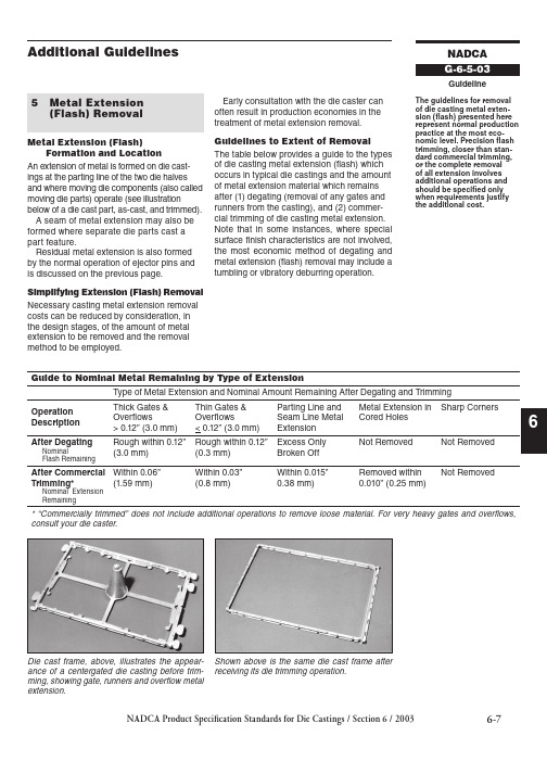
Metal Extension (Flash) Formation and Location
An extension of metal is formed on die castings at the parting line of the two die halves and where moving die components (also called moving die parts) operate (see illustration below of a die cast part, as-cast, and trimmed).
NADCA Product Specification Standards for Die Castings / Section 6 / 2003
6-7
ቤተ መጻሕፍቲ ባይዱ
Die cast frame, above, illustrates the appearance of a centergated die casting before trimming, showing gate, runners and overflow metal extension.
Shown above is the same die cast frame after receiving its die trimming operation.
NADCA
G-6-5-03
Guideline
The guidelines for removal of die casting metal extension (flash) presented here represent normal production practice at the most economic level. Precision flash trimming, closer than standard commercial trimming, or the complete removal of all extension involves additional operations and should be specified only when requirements justify the additional cost.
近红外光谱法测定芬布芬片中芬布芬的含量

近红外光谱法测定芬布芬片中芬布芬的含量1仪器及材料1.1 仪器高效液相色谱仪:(厂家:Thermo Fisher Scientific;型号:U3000 ;包括梯度泵SR-3000、自动进样器WPS-3000、柱恒温系统TCC-3000、紫外检测器VWD-3100、色谱工作站变色龙6.8 )色谱柱:phenomenex Luna 5u C18(2)(5μm,250×4.6mm)近红外光谱仪:美国JDSU MicroNIR TM 1700天平(厂家:梅特勒-托利多仪器(上海)有限公司;型号:XS205 DualRange 型十万分之一分析天平、AL104型万分之一分析天平)1.2材料芬布芬片(修正药业集团提供,生产批号:111201、111202、111203、111208、120301、120302、120303、120401、120501、121003、121004、121006、121201、121203、121204、121205、121206、121207、121209、130301);芬布芬对照品(购自中国药品生物制品检定所,供含量测定用);甲醇(色谱级);冰醋酸(分析纯);水为二次水2芬布芬含量测定方法学考察2.1色谱条件色谱柱:phenomenex Luna 5u C18(2)(5μm,250×4.6mm);流动相:1.8%冰醋酸溶液-乙腈(56:44)为流动相;流速1mL/min;等度洗脱;采集30min ;UV检测器,检测波长为280nm。
进样量10μl;柱温30 ℃。
2.2标准品溶液的配制取芬布芬对照品15mg,精密称定,置10ml量瓶中,加甲醇3ml,超声15分钟使溶解,用流动相稀释至刻度,摇匀,精密量取2ml置50ml量瓶中,用流动相稀释至刻度,摇匀,用微孔滤膜(0.45ul)滤过,取续滤液,即得。
(稀释250倍0.06mg/ml)2.3供试品溶液的制备取本品1片,精密称定,研细,精密称取适量(约相当与芬布芬0.075g),置50ml量瓶中,加甲醇30ml,超声15分钟使溶解,用流动相稀释至刻度,摇匀,滤过,精密量取续滤液2ml置50ml量瓶中,用流动相稀释至刻度,摇匀,用微孔滤膜(0.45ul)滤过,取续滤液,即得。