VOL. 39 Automatic Activity in Depolarized Guinea Pig
PCE-322A 类 II 声音级表 分贝表说明书

PCE Americas Inc.711 Commerce Way Suite 8JupiterFL-33458USAFrom outside US: +1 Tel: (561) 320-9162 Fax: (561) 320-9176*********************PCE Instruments UK Ltd.Units 12/13 Southpoint Business ParkEnsign way Hampshire / Southampton United Kingdom, SO31 4RF From outside UK: +44Tel: (0) 2380 98703 0Fax: (0) 2380 98703 9 ************************/englishTechnical Environmental Tester PCE-322APCE-322A Sound Level MeterClass II decibel (dB) meter with data-logging functionality / Measuring range: 30 ... 130 dB / Memory stores up to 32,700 readings / USB port / Microsoft Excel compatible / AnalogoutputPCE-322A is a handheld, portable, professional Class II sound level meter or decibel meter with built-in data-logging or data-recording functionality. Thus, PCE-322A is ideal for real-time noise measurement as well as for long-term noise exposure monitoring over time. A mini tripod is included in the delivery contents, as is a wind noise suppressor. The recorded decibel readings help users determine if and what protective measures need to be taken to ensure overall health, safety and productivity in industrial, commercial, occupational, educational and residential environments. The sound level meter can also be used to evaluate acoustics for audio installations.The sound level meter can be connected to a PC via the USB port. This allows the recorded decibel readings to be transferred to a PC for detailed analysis using Microsoft Excel or the included downloadable proprietary software. The sound level meter also features an analog output for connecting to a frequency analyzer or X-Y shaft recorder.- IEC 61672-1 Class II sound level meter- USB port for data transfer- Memory stores up to 32,700 readings- Fast and slow time weighting- A and C frequency weightings- Max, min, hold and alarm functions- Date- and time-stamped measurements- Analog output- Heavy-duty ABS plastic enclosure- Large, easy-to-read, 4-digit LCD screen- Power-saving automatic shutoff > 15 min. inactivity- Battery allows approx. 30 hours continuous use- ISO calibration available as an option - see accessories for detailsTechnical specifications:Noise levels Low 30 ... 80 dB Medium 50 ... 100 dB High 80 ... 130 dB Auto 30 ... 130 dBDynamic range 50 dBDisplay 4-digit LCD Resolution 0.1 dB Accuracy ±1.4 dB Sampling rate 2 x per second Frequency 31.5 Hz ... 8 kHz Storage capacity 32,700 readings Frequency weighting A and CTime weighting Fast (125 ms) Slow (1 sec.)Microphone type Electret condenser Functions MIN, MAX, HOLD, ALARMAnalog output AC/DC HeadphoneData interface USB portAutomatic shutdown After 15 minutes inactivityOperating conditions 0 ... +40 °C / +32 ... +104 °F, < 90 % RH Storage conditions -10 ... +60 °C / +14 ... +140 °F, 10 ... 75 % RHPower supply 9 V block battery (for approx. 30 h continuous operation) AC powerDimensions 280 x 95 x 45 mm / 11.02 x 3.74 x 1.77" Weight Approx. 350 g / 0.78 lbStandards IEC 61672-1 Class IIPlease see user manual for complete technical specifications. Delivery contents:1 x PCE-322A sound level meter1 x wind noise suppressor1 x USB cable1 x mini tripod1 x calibration screwdriver1 x battery1 x power adapter1 x carrying case1 x user manual。
Autolab 电位器和 NOVA 控制器程序的电化学测量说明书
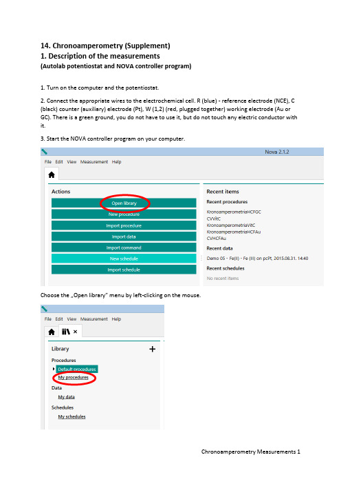
14. Chronoamperometry (Supplement)1. Description of the measurements(Autolab potentiostat and NOVA controller program)1. Turn on the computer and the potentiostat.2. Connect the appropriate wires to the electrochemical cell. R (blue) - reference electrode (NCE), C (black) counter (auxiliary) electrode (Pt), W (1,2) (red, plugged together) working electrode (Au or GC). There is a green ground, you do not have to use it, but do not touch any electric conductor with it.3. Start the NOVA controller program on your computer.Choose the …Open library” menu by left-clicking on the mouse.Clicking on the …My procedures” menu, you could find the procedures (programs) used in the measurements.Choose the appropriate procedure to what you want to do. Read the …Remarks” field also to choose the right program.For Chronoamperometric measurements, the parameters given in the measurement description are already set. The procedure looks like this.Each icon indicates "Commands", which makes the measurement happen. The first icon, "Autolab control" is used to detect the measuring instrument, to set the potentiostatic mode, and to select the current range. The second icon, "Apply", sets the initial electrode potential at the input of the potentiostat. The third icon, "Cell on", connects the potentiostat to the electrochemical cell. The fourth icon, "Wait", keeps the working electrode for the specified time at the initial potential. The fifth icon, "Apply", indicates the potential step to the specified value. The sixth icon, "Record signals", performs the measurement of the time depending current after the potential step. The seventh icon, "Cell Off" turns the cell off from the potentiostat, finishes the measurement. The measurement procedure and the measured data are automatically saved in a .nox file that can be found later on the "My data" menu in the "Library" menu. The data file name is the file name of the "Procedure" plus a "Timestamp", i.e. when the measurement was made. Therefore, it is important to note the order of measurements so that their results can easily be found later.The measurement can be started by clicking on the "Run" command in the "Measurement" menu on the top of the screen or by clicking the Play ( ) icon above the Procedure.During the measurement, instead of the Play icon, the Pause ( ) and Stop ( ) icons will be displayed. If you notice a problem, stop the measurement.During the measurement, the computer automatically plots the measured data in the Plots window in the lower left corner of the screen.Physically, the data files are stored in the Dokumentumok Library in the NOVA 2.1 folder in the Data subfolder. From there, you can make a copy, e.g. to a pendrive.…Behind” each Command icon you could find "Subcommands", shown on the right side of the Procedure pane, or you can see the details with the "More" command by clicking on the corresponding icon. If it is possible, do not change the parameters, or if this happened, DO NOT SAVE THE ALTERED PROCEDURE WITH ITS ORIGINAL NAME.For cyclic voltammetric measurements, the "Procedure" looks like this:Each icon indicates "Commands", which makes the measurement happen. The first icon, "Autolab control" (Autolab control) is used to detect the measuring instrument, to set the potentiostatic mode, and to select the current range. The second icon, "Message", asks for the applicable scan rate ("Scan rate (V/s)"). Once the measurement is started, it must be set to the desired value. The third icon, "Apply", sets the initial electrode potential at the input of the potentiostat. The fourth icon, "Cell on", switches the potentiostat to the electrochemical cell. The fifth icon, "Wait", keeps the working electrode for the specified time at the initial potential. The sixth icon, "CV staircase", represents the cyclic measurement between the lower and upper potential limits with the scan rate given in the …Message". The seventh icon, "Cell Off" turns the cell off from the potentiostat, finishes the measurement. The measurement procedure and the measured data are automatically saved in a .nox file that can be found later on the "My data" menu in the "Library" menu. The data file name is the file name of the "Procedure" plus a "Timestamp", i.e. when the measurement was made. Therefore, it is important to note the order of measurements so that their results can easily be found later.The measurement can be started by clicking on the "Run" command in the "Measurement" menu on the top of the screen or by clicking the Play ( ) icon above the Procedure.During the measurement, instead of the Play icon, the Pause ( ) and Stop ( ) icons will be displayed. If you notice a problem, stop the measurement.During the measurement, the computer automatically plots the measured data in the Plots window in the lower left corner of the screen.Physically, the data files are stored in the Dokumentumok Library in the NOVA 2.1 folder in the Data subfolder. From there, you can make a copy, e.g. to a pendrive.…Behind” each Command icon you could find "Subcommands", shown on the right side of the Procedure pane, or you can see the details with the "More" command by clicking on the corresponding icon. If it is possible, do not change the parameters, or if this happened, DO NOT SAVE THE ALTERED PROCEDURE WITH ITS ORIGINAL NAME.The only parameter you have to set is "Scan rate (V/s)". For sequential runs, use the order that is described in the measurement description. (For example HCF solutions 0.320 V/s, 0.160 V/s, 0.080V/s, etc.)IMPORTANT! NOVA uses Windows default decimal separator. See that the "Message" contains the default value, and that the entered value is also correct! (For example, 0,08 or 0.08!) The data exported from the NOVA also uses the same decimal separator. If necessary, change it to the settings in the Excel Options menu in accordance with the Windows setup!2. Description of evaluation(Autolab potentiometer and NOVA controller program)The NOVA software used for the measurements can be applied for many purposes, but the User's manual is 1196 pages, which is a bit tiring in a lab to read. Therefore, only the most important functions are highlighted.For the evaluation of voltammograms, it is necessary to determine the peak potentials (E p), half peak current potentials (E p/2) and the background corrected peak currents (I p). This can be done in Excel after exporting the measurement data. To do this, double-click the "Plots" pane.Instead of the procedure, the measured plot is displayed in the main window.Clicking on the …Show data” icon you could see a table.In the top right corner there is a marker leading to the export function.Select Excel Export from "File Format", and Windows Explorer will save the file to the desired name and location.ATTENTION! The Excel file contains only the measured data (maybe calculated data, as well), not the description of the Procedure! It's still in the .nox files, do not delete them.IMPORTANT! NOVA uses Windows default decimal separator. The data exported from the NOVA also uses the same decimal separator. If necessary, change it to the settings in the Excel Options menu in accordance with the Windows setup!For Excel files, you can get the desired data, graphics, where needed.For the evaluation of voltammograms, it is necessary to determine the peak potentials (E p), half peak current potentials (E p/2) and the background corrected peak currents (I p). This can be done in Excel after exporting the measurement data, but (perhaps) simpler in NOVA with an "Analysis" function.Click the microscope icon to see a menu. Select "Peak search" analysis.Then, a submenu "Properties" opens in the right window, which offers different versions of the peak search. The default setting is "Automatic", and the figure (or the table) also shows this result, but this is usually good for nothing!Select "Manual", and "Linear free cursor" option.Returning to the plot in the main window with the mouse, you could see a cross. Set this to the initial part of the voltammogram, and fix it with a click. Drag a straight line with the mouse that best fits thefirst part of the voltammogram. The end of the line does not have to be on the curve (free cursor). You can fix the straight line with another click, and the results of the peak search appear in the "Properties" window on the right. (Another voltammogram is illustrated because there will be many peaks on the earlier example.)The same can also be done for the cathodic peak, however from the other end of the curve, the straight line must be fitted backwards.All of these can go in succession, the peaks are included in the right table ("Peaks"). If you are not satisfied with the fitting, you can resume the search at any time by pressing the "Reset" button.The values in the table are:1 Number of found peaks"Peak position" is the electrode potential of the found peak in Volt"Peak height" is the corrected value of the peak current in Amper"Peak (1/2)" is the difference between the potential at the peak current and the potential at the half peak current, i.e. Peak (1/2) = E p– E P/2. (Signed!) (The other columns are not interesting now!)Data can not be exported directly, but when the data is marked with the mouse you can use Ctrl-C to put those on the clipboard, and then use the command Ctrl-V, for example, to copy those to Excel. Only the data, the header will not pass! Afterwards, you can delete unnecessary parts. IMPORTANT! NOVA uses Windows default decimal separator. The data exported (or copied) from NOVA also uses the same decimal separator. If necessary, change it to the settings in the Excel Options menu in accordance with the Windows setup!For chronoamperometric measurements it is recommended to integrate (calculate the charge-time function) in NOVA (you could spare an Excel programming). In the "Plot" window, call up the "Integrate" analysis command!The result is a new figure and the extension of the data file with integrated values.Exporting the measurement results to Excel will include the measured currents and the calculated charge as well.The rest are just time, patience and lots of work, and the evaluation is ready!14. Chronoamperometry1. Description of the measurements(Autolab potentiostat and NOVA controller program)IMPORTANT SUPPLEMENTAfter each electrode exchange and / or solution change, the first thing is a cell control!To do this, select "OCPMeasurement" from the "My procedures" list. The procedure looks like this.The first icon, "Autolab control", is used to detect the measuring instrument and to set the potentiostatic mode. The second icon, "Cell on", connects the potentiostat to the electrochemical cell. The third icon "OCP" (Open Circuit Potential) begins to measure the potential difference between the working and reference electrodes (OCP) when no current flows (the electric circuit is open between the working and the counter electrode). The fourth icon "Cell Off" turns the cell off the potentiostat, finishes the measurement.If, after starting the measurement, it is found that the difference between the Minimum and Maximum Potential is too high, or the blue line indicating the time dependence of the time derivative of the electrode potential (dE/dt) shows too high values (V/s and not μV/s), interrupt the measurement with the "Abort" command. THERE IS SOME TROUBLE!It is likely that the working and / or the reference electrode is not properly connected, the system can not be used! (The system did not damage yet because there was no current during the measurement!) Check the connections and run the procedure again.R (blue) reference electrode (NCE), C (black) counter (auxiliary) electrode (Pt), W (1,2) (red, plugged together) working electrode (Au or GC). There is a green ground, you do not have to use it, but do not touch any electric conductor with it.If, after starting the measurement, it is found that the deviation between the Minimum and Maximum Potential is small max. 10-20 mV, and the blue line indicating the time dependence of the time derivative of the electrode potential (dE/dt) shows normal (mV/s or μV/s) values, you can interrupt the measurement with the "Abort" command. The cell connection is OK!The measurement procedure and the measured data are automatically saved in a .nox file that can be found later in the "My data" menu in the "Library" menu. The data file name is called "OCPMeasurement" plus a "Timestamp", i.e. when the measurement was made. These files should normally not be used at the time of evaluation, but only for diagnostic purposes.。
Sennheiser ew 系列无线麦克风系统用户手册说明书

The ew 322 G3 consists of the same components as ew 312 G3but with a compact cardioid clip-on microphone.The ew 352 G3 consists of the same components as ew 312 G3but with a headworn cardioid microphone.FEATURESSturdy metal housing(transmitter and receiver)42 MHz bandwidth: 1,680 tunable UHF frequencies for interference-free reception20 frequency banks with up to 24 compatible frequenciesEthernet port for connecting to theWireless Systems Manager (WSM) software for control via computer High-quality true diversity receptionPilot tone squelch for eliminating RF inter- ference when transmitter is turned off Automatic frequency scan feature searches for available frequencies Enhanced AF frequency rangeIncreased range for audio sensitivity Wireless synchronization of transmitter parameter from receiverUser-friendly menu operation with more control optionsIlluminated graphic display, receiver also shows transmitter settingsAuto-Lock function avoids accidental changing of settingsHDX compander for crystal-clear sound Transmitter feature battery indicatation in 4 steps, also shown on receiver display Programmable Mute function Integrated Equalizer and Soundcheck modeContacts for recharging BA 2015 accupack directly in the transmitter Wide range of accessories adapts the system to any requirementThe ew 312 G3 is a wireless microphone set, consisting of a True Diversityreceiver, a bodyworn transmitter, a compact omni directional clip-on micropho-ne plus accessories.The bodypack transmitter features charging contacts for the optional recharge-able battery. Sync up the bodypack to the receiver wirelessly with the new wireless sync. Backlit graphic displays make them easy to read under all lighting conditions.ew 300 Setsew 312 G3 Presentation Set ew 322 G3 Presentation Set ew 352 G3 Head Setew 335/345/365 G3 Vocal SetsFEATURESew 335 G3/ew 345 G3/ew 365 G3 Vocal SetsSee above mentioned list of features plus Programmable Mute switch, easyaccessableHandheld transmitter with easy-exchangeable microphone heads from evolution series The ew 335 G3 is a wireless microphone set, consisting of a True Diversity receiver, a handheld transmitter with e 835 microphone head plus accessories. It is versatile for every style of music and presentations. A wireless link from receiver to the transmitter allows synchronization of frequencies for easy setup. Backlit graphic displays make them easy to read under all lighting conditions. The ew 345 G3 consists of the same components as ew 335 G3but with an e 845 microphone head.The ew 365 G3consists of the same components as ew 335 G3but with an e 865 microphone head.ARCHITECT’S SPECIFICATIONSew 312 G3 Presentation SetComplete plug & play wireless microphone set with clip-on microphone (condenser, omni-directional) from Sennheiser evolution series for multi-purpose application. The devices shall have metal housings for rugged use. 42 MHz bandwidth with 1,680 tunable frequencies. 20 banks with up to 24 compatible frequencies, 1 bank for individual selectable frequencies, scan function and wireless synchronization to the transmitter for easy setup. HDX compander delivers high-quality sound performance. All parameters of transmitter and receiver can be monitored and controlled via Wireless Systems Manager (WSM) software from PC. The transmitter shall have a sensitivity range of 48 dB. The receiver offers a maximum output level of +18 dBu (+6 dB gain). True Diversity and pilot tone squelch for interference-free reception. Charging contacts on transmitter for recharging BA 2015 accupack directly in the transmitter shall be available. 3-step battery + LowBattery indication on transmitter and receiver shall give reliable information on operation time.Menu operation, auto-lock function and illuminated graphic displays on transmitter and receiver for user-friendly operation.A RF Mute function on transmitter and receiver allows offline settings.An easy accessable Mute switch on the transmitter can be programmed for AF on/off, RF on/off.A suitable Remote Mute Switch option also allows push-to-talk and push-to-muteAn equalizer and soundcheck mode is inte g rated in the receiver.ew 322 G3 Presentation SetComplete plug & play wireless microphone set with clip-on microphone (electret, cardioid) from Sennheiser evolution series for multi-purpose application. Further discription see paragraph ew 312 G3.ew 352 G3 Head SetComplete plug & play wireless microphone set with headworn microphone (condenser, cardioid) for hands-free application. Further discription see paragraph ew 312 G3.ew 335 G3 Vocal SetComplete plug & play wireless microphone set with easy-exchangeable e 835 microphone head (dynamic, cardioid) from Sennheiser evolution series for multi-purpose application. Further discription see paragraph ew 312 G3.ew 345 G3 Vocal SetComplete plug & play wireless microphone set with easy-exchangeable e 845 microphone head (dynamic, supercardioid) from Sennheiser evolution series for multi-pur p ose application. Further discription see paragraph ew 312 G3.ew 365 G3 Vocal SetComplete plug & play wireless microphone set with easy-exchangeable e 865 microphone head (electret-condenser, supercardioid) from Sennheiser evolution series for multi-purpose application. Further discription see paragraph ew 312 G3.SySTEMRF frequency range ................................................516.....865 MHzTransmission/receiving frequencies ...................1,680Frequency banks ..................................................... 20 (factory presets)6 (user presets)Presets .......................................................................24 max.Switching bandwidth .............................................42 MHzCompander ...............................................................HDXSignal-to-noise ratio ..............................................> 115 dB(A)THD, total harmonic distortion ............................< 0.9 %RECEIvERAF Frequency response..........................................25…18,000 HzAntenna connectors ...............................................BNC, 50 OhmAudio outputs .......................................................... X LR: +18 dBu max6.3 mm jack: +10 dBu maxDimensions ...............................................................212 x 202 x 43 mmWeight .......................................................................980 gTRANSMITTERRF output power .....................................................10/30 mW switchableOperating time ........................................................typ. 8hInput voltage range ................................................1.8 v lineInput voltage range ................................................2.4 v lineDimensions ...............................................................82 x 64 x 24 mmWeight .......................................................................~ 160 gMICROPHONETransducer; Microphone type ...............................permanent polarizedAF sensitivity ...........................................................1.6 mv/PaFrequency response ...............................................80.....18,000 HzPick-up pattern ........................................................omni-directionalContinued on page 5EM 300Modulation ...............................................................wideband FMRF frequency range ................................................ 516 – 558, 566 – 608, 626 – 668, 734 –776, 780 – 822, 823 – 865 MHz Transmission/receiving frequencies ...................1,680, tuneable in steps of 25 kHzReceiving frequencies ............................................ 1,680 frequencies, tuneable in steps of 25 kHz20 frequency banks, each with up to 24 factory-preset channels,intermodulation-free20 frequency banks with up to 24 user programmable channelsSwitching bandwidth .............................................42 MHzNominal/peak deviation .......................................±24 kHz/±48 kHzReceiver principle ....................................................true diversitySensitivity (with HDX, peak deviation) .............< 2 μv for 52 dBA rms S/NAdjacent channel rejection ...................................typ. ≥ 75 dBIntermodulation attenuation ...............................typ. ≥ 70 dBBlocking .....................................................................≥ 75 dBSquelch ...................................................................... O ff, 5 to 25 dBμv, adjustable in steps of 2 dBPilot tone squelch ...................................................can be switched offAntenna inputs .......................................................2 BNC socketsCompander system .................................................Sennheiser HDXEQ presets (switchable, affect the line and monitor outputs):Preset 1: “Flat”Preset 2: “Low Cut” ................................................–3 dB at 180 HzPreset 3: “Low Cut/High boost” .......................... –3 dB at 180 Hz+6 dB at 10 kHzPreset 4: “High Boost” ...........................................+6 dB at 10 kHzS/N ratio (1 mv, peak deviation) ........................≥ 115 dBATHD .............................................................................≤ 0.9 %AF output voltage (at peak deviation,1 kHz AF) .................................................................. ¼” (6.3 mm) jack socket (unbalanced): +12 dBuXLR socket (balanced): +18 dBuAdjustment range of audio output level ........... 48 dB, adjustable in steps of 3 dB +6 dB gain reserveTemperature range .................................................–10 °C to +55 °CPower supply............................................................12 vPower consumption:...............................................350 mADimensions ...............................................................approx. 202 x 212 x 43 mmWeight (incl. batteries) .........................................approx. 980 gIn compliance with .................................................. C E, FCC, ETS 300422, ETS 300445MAINS UNITInput voltage............................................................100 to 240 v~, 50/60 HzPower/current consumption ................................max. 120 mAOutput voltage ........................................................12 vSecondary output current .....................................400 mATemperature range .................................................–10 °C to +40 °CIn compliance with .................................................. C E, FCC, IC, ETS 300422, ETS 300445Continued on page 6SK 300 and SKM 300Modulation ...............................................................wideband FMRF frequency range ................................................ 516 – 558, 566 – 608, 626 – 668, 734 –776, 780 – 822, 823 – 865 MHz Transmission/receiving frequencies ...................1,680, tuneable in steps of 25 kHzReceiving frequencies ............................................ 1,680 frequencies, tuneable in steps of 25 kHz20 frequency banks, each with up to 24 factory-preset channels, intermodulation-free6 frequency banks with up to 24 user programmable channelsSwitching bandwidth .............................................42 MHzNominal/peak deviation .......................................±24 kHz/±48 kHzFrequency stability .................................................≤ ±15 ppmRF output power at 50 O......................................typ. 10/30 mW, switchablePilot tone squelch ...................................................can be switched offAF characteristicsCompander system .................................................Sennheiser HDXAF frequency responseSK ................................................................................ m icrophone: 80 –18,000 Hzline: 25 –18,000 HzSKM ............................................................................80 –18,000 HzS/N ratio (1 mv, peak deviation) ........................≥ 115 dBATHD .............................................................................≤ 0.9 %Max. input voltage (SK) microphone/line ........3 vrmsInput impedance (SK) microphone/line ...........40 k O, unbalanced/1 M OInput capacitance (SK) ..........................................switchableAdjustment range of input sensitivity .............. S K: 60 dB, adjustable in steps of 3 dBSKM: 48 dB, adjustable in steps of 6 dBIn compliance with .................................................. C E, FCC, IC, ETS 300422, ETS 300445OvERALL DEvICETemperature range .................................................−10 °C to + 55 °CPower supply ........................................................... 2 AA size batteries, 1.5 v orBA 2015 accupackNominal voltage .....................................................2.4 vCurrent consumption: at nominal voltage ........typ. 180 mA (30 mW)with switched-off transmitter .............................≤ 25 μAOperating time .......................................................typ. 8 hrsDimensions ............................................................... S K: approx. 82 x 64 x 24 mmSKM: approx. Ø 50 x 265 mmWeight (incl. batteries) ......................................... S K: approx. 160 gSKM: approx. 450 gIn compliance with .................................................. C E, FCC, IC, ETS 300422, ETS 300445Continued on page 7Microphones (SK 300)ME 2ME 3-ew ME 4Microphone type .............................condenser condenser condenserSensitivity .........................................20 mv/Pa 1.6 mv/Pa40 mv/PaPick-up pattern ................................omni-directional cardioid cardioidMax. SPL ............................................130 dB SPL150 dB SPL120 dB SPL Microphone heads (SKM 300)MMD 835-1MMD 845-1MMK 865-1Radio microphone type .................dynamic dynamic condenserSensitivity ......................................... 2.1 mv/Pa 1.6 mv/Pa 1.6 mv/PaPick-up pattern ................................cardioid super-cardioid cardioid/super-cardioid,switchableMax. SPL ............................................154 dB SPL154 dB SPL152 dB SPL Frequency response .......................80.....18,000 Hz80.....18,000 Hz80.....18,000 HzDELIVERY INCLUDES for ew 312 / ew 322 / ew 352 G31 EM 300 G3 rack-mount receiver1 SK 300 G3 bodypack transmitter1 ME2 clip-on microphone (omni-directional) or1 ME 4 clip-on microphone (cardioid) or1 ME 3-ew headset microphone (cardioid)1 GA 3 rack mount1 NT2 power supply unit2 Antennas2 AA batteries1 Instruction manualDELIVERY INCLUDES for ew 335 / ew 345 / ew 365 G31 S KM 300-835 handheld transmitterwith cardioid dynamic head or1 S KM 300-845 handheld transmitterwith super-cardioid dynamic head or1 S KM 300-865 handheld transmitterwith super-cardioid condenser head1 EM 300 G3 rack receiver1 MZQ 1 microphone clip1 NT2 power supply unit2 Antennas1 GA 3 Rack mount kit2 AA batteries1 Instruction ManualPOLAR PATTERN0510152025dB30°30°60°60°90°90°120°150°120°150°0°180°125 Hz 250 Hz 500 Hz 1000 Hz2000 Hz 4000 Hz 8000 Hz 16000 HzMMD 835-1MME 865-1MMD 845-10510152025dB30°30°60°60°90°90°120°150°120°150°0°180°125 Hz 250 Hz 500 Hz 1000 Hz2000 Hz 4000 Hz 8000 Hz 16000 Hz0510152025dB30°30°60°60°90°90°120°150°120°150°0°180°125 Hz 250 Hz 500 Hz 1000 Hz2000 Hz 4000 Hz 8000 Hz 16000 HzME 3-ewME 4-ew0510152025dB30°30°60°60°90°90°120°150°120°150°0°180°125 Hz 250 Hz 500 Hz 1000 Hz2000 Hz 4000 Hz 8000 Hz 16000 Hz0510152025dB30°30°60°60°90°90°120°150°120°150°0°180°125 Hz 250 Hz 500 Hz 1000 Hz2000 Hz 4000 Hz 8000 Hz 16000 HzPRODUCT VARIANTSew 312 G3 Presentation Set Cat. No. ew 312 G3-A-EU 516 – 558 MHz 503112 ew 312 G3-A-US 516 – 558 MHz 503330 ew 312 G3-G-EU 566 – 608 MHz 503331 ew 312 G3-G-US 566 – 608 MHz 503332 ew 312 G3-B-EU 526 – 668 MHz 503333 ew 312 G3-B-US 526 – 668 MHz 503334 ew 312 G3-C-EU 734 –776 MHz 503335 ew 312 G3-C-US 734 –776 MHz 503336 ew 312 G3-D-EU 780 – 822 MHz 503337 ew 312 G3-D-EU-X 780 – 822 MHz 503338 ew 312 G3-D-UK 780 – 822 MHz 503339 ew 312 G3-E-EU 823 – 865 MHz 503340 ew 312 G3-E-EU-X 823 – 865 MHz 503341 ew 312 G3-E-UK 823 – 865 MHz 503342 ew 312 G3-GB 606 – 648 MHz 504649 ew 322 G3 Presentation Set Cat. No. ew 322 G3-E-UK 823 – 865 MHz 503357 ew 322 G3-A-EU 516 – 558 MHz 503113 ew 322 G3-A-US 516 – 558 MHz 503345 ew 322 G3-G-EU 566 – 608 MHz 503346 ew 322 G3-G-US 566 – 608 MHz 503347 ew 322 G3-B-EU 626 – 668 MHz 503348 ew 322 G3-B-US 626 – 668 MHz 503349 ew 322 G3-C-EU 734 –776 MHz 503350 ew 322 G3-C-US 734 –776 MHz 503351 ew 322 G3-D-EU 780 – 822 MHz 503352 ew 322 G3-D-EU-X 780 – 822 MHz 503353 ew 322 G3-D-UK 780 – 822 MHz 503354 ew 322 G3-E-EU 823 – 865 MHz 503355 ew 322 G3-E-EU-X 823 – 865 MHz 503356 ew 322 G3-GB 606 – 648 MHz 504650 ew 352 G3 Presentation Set Cat. No. ew 352 G3-A-EU 516 – 558 MHz 503114 ew 352 G3-A-US 516 – 558 MHz 503360 ew 352 G3-G-EU 566 – 608 MHz 503361 ew 352 G3-G-US 566 – 608 MHz 503362 ew 352 G3-B-EU 526 – 668 MHz 503363 ew 352 G3-B-US 526 – 668 MHz 503364 ew 352 G3-C-EU 734 –776 MHz 503365 ew 352 G3-C-US 734 –776 MHz 503366 ew 352 G3-D-EU 780 – 822 MHz 503367 ew 352 G3-D-EU-X 780 – 822 MHz 503368 ew 352 G3-D-UK 780 – 822 MHz 503369 ew 352 G3-E-EU 823 – 865 MHz 503370 ew 352 G3-E-EU-X 823 – 865 MHz 503371 ew 352 G3-E-UK 823 – 865 MHz 503372 ew 352 G3-GB 606 – 648 MHz 504651ew 335 G3 Vocal Set Cat. No. ew 335 G3-A-EU 516 – 558 MHz 503115 ew 335 G3-A-US 516 – 558 MHz 503375 ew 335 G3-G-EU 566 – 608 MHz 503376 ew 335 G3-G-US 566 – 608 MHz 503377 ew 335 G3-B-EU 526 – 668 MHz 503378 ew 335 G3-B-US 526 – 668 MHz 503379 ew 335 G3-C-EU 734 –776 MHz 503380 ew 335 G3-C-US 734 –776 MHz 503381 ew 335 G3-D-EU 780 – 822 MHz 503382 ew 335 G3-D-EU-X780 – 822 MHz 503383 ew 335 G3-D-UK 780 – 822 MHz 503384 ew 335 G3-E-EU 823 – 865 MHz 503385 ew 335 G3-E-EU-X823 – 865 MHz 503386 ew 335 G3-E-UK 823 – 865 MHz 503387 ew 335 G3-GB 606 – 648 MHz 504652 ew 345 G3 Vocal Set Cat. No. ew 345 G3-A-EU 516 – 558 MHz 503116 ew 345 G3-A-US 516 – 558 MHz 503390 ew 345 G3-G-EU 566 – 608 MHz 503391 ew 345 G3-G-US 566 – 608 MHz 503392 ew 345 G3-B-EU 526 – 668 MHz 503393 ew 345 G3-B-US 526 – 668 MHz 503394 ew 345 G3-C-EU 734 –776 MHz 503395 ew 345 G3-C-US 734 –776 MHz 503396 ew 345 G3-D-EU 780 – 822 MHz 503397 ew 345 G3-D-EU-X780 – 822 MHz 503398 ew 345 G3-D-UK 780 – 822 MHz 503399 ew 345 G3-E-EU 823 – 865 MHz 503400 ew 345 G3-E-EU-X823 – 865 MHz 503401 ew 345 G3-E-UK 823 – 865 MHz 503402 ew 345 G3-GB 606 – 648 MHz 504653 ew 365 G3 Vocal Set Cat. No. ew 365 G3-A-EU 516 – 558 MHz 503117 ew 365 G3-A-US 516 – 558 MHz 503405 ew 365 G3-G-EU 566 – 608 MHz 503406 ew 365 G3-G-US 566 – 608 MHz 503407 ew 365 G3-B-EU 526 – 668 MHz 503408 ew 365 G3-B-US 526 – 668 MHz 503409 ew 365 G3-C-EU 734 –776 MHz 503410 ew 365 G3-C-US 734 –776 MHz 503411 ew 365 G3-D-EU 780 – 822 MHz 503412 ew 365 G3-D-EU-X780 – 822 MHz 503413 ew 365 G3-D-UK 780 – 822 MHz 503414 ew 365 G3-E-EU 823 – 865 MHz 503415 ew 365 G3-E-EU-X823 – 865 MHz 503416 ew 365 G3-E-UK 823 – 865 MHz 503417 ew 365 G3-GB 606 – 648 MHz 504654RECOMMENDED ACCESSORIESCat. No. ME 4-ew – Clip-on microphone,cardioid, black 503156 AM 2 – Antenna Mount kit 009912 CC 3 – System Case 503168L 2015 – Charging unit 009928 BA 2015 – Rechargeable battery pack 009950 ASA 1 – Active antenna splitter 503165 NT 1-1 – plug-in mains unit forASA 1 & L 2015 E U: 503158US: 503873UK: 503874 NT 3-1 – Plug-in mains unit for L 2015 E U: 503159US: 503876UK: 503877 A 1031-U – Antenna 004645A 2003-UHF – Directional Antenna 003658 AB 3 – Antenna booster 505550 Ear Set 1-ew – Ear-worn microphone,omni, black 504232 Ear Set 1-ew-3 – Ear-worn microphone,omni, beige 504237 Ear Set 4-ew – Ear-worn microphone,cardioid, black 504236 Ear Set 4-ew-3 – Ear-worn microphone,cardioid, beige 504234 MKE 1-ew – Clip-on microphone,omni-directional, black 502876 MKE 1-ew-1 – Clip-on microphone,omni, white 502877 MKE 1-ew-2 – Clip-on microphone,omni, brown 502878 MKE 1-ew-3 – Clip-on microphone, beige 502879 MKE 2-ew Gold – Clip-on microphone,omni, black 009831 MKE 2-ew-3 Gold – Clip-on microphone,omni, beige 009832 MKE 40-ew – Clip-on microphone,cardioid, black 500527Cat. No. HSP 4-ew – Headworn microphone,cardioid, black 009864 HSP 4-ew-3 – Headworn microphone,cardioid, beige 009867 HSP 2-ew – Headworn microphone,omni, black 009866 HSP 2-ew-3 – Headworn microphone,omni, beige 009872 CI 1 – Instrument cable 503163ew 335 / ew 345 / ew 365 G3 Vocal SetsMMD 835-1 – evolution microphone head 502575 MMD 845-1 – evolution microphone head 502576 MME 865-1 – evolution microphone head 502581 MZW 1 – Windshield 004839 KEN 2 – Identification rings 530195 LA 2 – Charging adapter forhandheld microphones 503162 CC 3 – System case 503168Sennheiser electronic GmbH & Co. KG Am Labor 1, 30900 Wedemark, Germany 0 4 / 1 3 S e n n h e i s e r i s a r e g i s t e r e d t r a d e m a r k o f S e n n h e i s e r e l e c t r o n i c G m b H & C o . K G . w w w . s e n n h e i s e r . c o m . C o p y r i g h t ©0 4 / 2 0 1 3 . A l l r i g h t s r e s e r v e d . E r r o r s a n d o m i s s i o n s e x c e p t e d .Contact your local Service Partner:。
SDRplay ADS-B (dump1090) User Guide

Radio Spectrum Processor ADS-B (dump1090) User GuideOverviewThe SDRplay Radio combines together the Mirics flexible tuner front-end and USB Bridge to produce a SDR platform capable of being used for a wide range of worldwide radio and TV standards. This document provides an overview of the installation process and operation of the SDRplay ADS-B(dump1090) application.Dump1090 was originally written by Salvatore Sanfilippo ***************** in 2012 and is released under the BSD three clause license.Malcolm Robb *********************** made a number of improvements in 2014. In this revision of the application, support has been added for the RSP.Oliver Jowett ********************.uk created mutability version including oversampled demod in 2016. Contents1.Installation (2)2.Getting Started (11)3.RSP Command Line Options (13)4.Legal Information (14)1. InstallationDownload the SDRplay ADS-B (dump1090) installer from the Windows section of the website (/downloads)Run the downloaded installation file and you will see this, click Yes to continue.Click Next to continue past the welcome screen.Please read and accept the license agreement.The next screen will display important information about these early releases. Read and then click Next.The next screen shows the installation directory. Check you have enough disk space and then click NextThe next screen confirms where the software will be installed to. If correct, click Install.After the software has installed, there will be some quick tips in the next screen, after you have reviewed these click Next.This completes the installation, clicking Finish will close the installer.This software works well with the Virtual Radar Server software. Virtual Radar Server will collect the data from dump1090 and produce a clickable map that shows all of the aircraft found by dump1090 in real time. You can download it from here: /Download.aspxAfter downloading the software, run it to start the installation.Click Next to continue past the welcome screen.Review and accept the license agreement, then click Next.You can review the change log and then click Next to continue.Review the installation directory and click NextThe next screen allows you to change the port number that the server listens on to receive web requests. You can normally leave this as the default (80) but if it conflicts with another web server you may have on your system, you can change it, then click Next.You can choose which folder to store the programs shortcuts or leave it as the default and click NextThis screen allows you to automatically configure the firewall to allow remote connections. Review this information and then click Next once you have decided on the correct setting.After reviewing the summary of what will be installed, click Install to begin.After the software has installed, click Finish to close the installer.2. Getting StartedThe easiest way to get started is to click on Start dump1090 from the Stat Menu (underSDRplay/dump1090). This will start dump1090 with settings to output the received plane information to the network ports.A receiver should be setup in Virtual Server with the following information:Format: BeastIP: 127.0.0.1 (if dump1090 and virtual server running on the same machine) or set to the IP address of the machine running dump1090Port: 30005 (this is the default output port for beast data)Please note: there are more Start options from the menu, these are 2MHz mode (interactive or quiet) and 8MHz mode (interactive or quiet). Interactive will show the plane information as received but will require more CPU than the quiet mode that just outputs the data to the network port.Whilst this is running, start Virtual Radar Server from the Start Menu. It should automatically connect to the dump1090 application and start to process incoming data.You can now click on the link in blue inside the Virtual Radar window (shown in blue) and it will open up a browser window showing the aircraft being detected on a map.You can change some of the command line options to try to improve the performance to capture more aircraft data. Below are some of the options that relate directly to the operation of the RSP.3. RSP Command Line Options--dev-sdrplay – Must be set for ANY RSP--net – enable networking--modeac – enable decoding of SSR modes 3/A & 3/C--oversample – use the 8MHz demodulator (default: 2MHz demodulator)--rsp-device-serNo <serNo> Used to select between multiple devices when more than one RSP device is present--rsp2-antenna-portA Select Antenna Port A on RSP2 (default Antenna Port B)--rspduo-tuner1 Select Tuner 1 on RSPduo (default Tuner 2 if Master or Single Tuner)--rspduo-single Use Single Tuner mode for RSPduo if available (default Master/Slave mode)--adsbMode Set SDRplay ADSB mode (default 1 for ZIF and 2 for LIF)--enable-biasT Enable BiasT network on RSP2 Antenna Port B or RSP1A or RSPduo Tuner 2--disable-broadcast-notch Disable Broadcast notch filter (RSP1A/RSP2/RSPduo)--disable-dab-notch Disable DAB notch filter (RSP1A/RSPduo)--interactive – display aircraft data in a table in the command prompt--quiet – Disable output to the command promptFor more information contact /support4. Legal Information********************************************************(2012)andisreleasedunderthefollowingBSDthreeclause license.**********************************(2014)madeanumberofimprovements******************************(2016)addedRSPsupportCopyright(c)2012,************************************All rights reserved.Redistribution and use in source and binary forms, with or without modification, are permitted provided that the following conditions are met:1. Redistributions of source code must retain the above copyright notice, this list of conditions and the following disclaimer.2. Redistributions in binary form must reproduce the above copyright notice, this list of conditions and the following disclaimer in the documentation and/or other materials provided with the distribution.3. Neither the name of the copyright holder nor the names of its contributors may be used to endorse or promote products derived from this software without specific prior written permission.THIS SOFTWARE IS PROVIDED BY THE COPYRIGHT HOLDERS AND CONTRIBUTORS "AS IS" AND ANY EXPRESS OR IMPLIED WARRANTIES, INCLUDING, BUT NOT LIMITED TO, THE IMPLIED WARRANTIES OF MERCHANTABILITY AND FITNESS FOR A PARTICULAR PURPOSE ARE DISCLAIMED. IN NO EVENT SHALL THE COPYRIGHT HOLDER OR CONTRIBUTORS BE LIABLE FOR ANY DIRECT, INDIRECT, INCIDENTAL, SPECIAL, EXEMPLARY, OR CONSEQUENTIAL DAMAGES (INCLUDING, BUT NOT LIMITED TO, PROCUREMENT OF SUBSTITUTE GOODS OR SERVICES; LOSS OF USE, DATA, OR PROFITS; OR BUSINESS INTERRUPTION) HOWEVER CAUSED AND ON ANY THEORY OF LIABILITY, WHETHER IN CONTRACT, STRICT LIABILITY, OR TORT (INCLUDING NEGLIGENCE OR OTHERWISE) ARISING IN ANY WAY OUT OF THE USE OF THIS SOFTWARE, EVEN IF ADVISED OF THE POSSIBILITY OF SUCH DAMAGE.SDRPlay modules use a Mirics chipset and software. The information supplied hereunder is provided to you by SDRPlay under license from Mirics. Mirics hereby grants you a perpetual, worldwide, royalty free license to use the information herein for the purpose of designing software that utilizes SDRPlay modules, under the following conditions:There are no express or implied copyright licenses granted hereunder to design or fabricate any integrated circuits or integrated circuits based on the information in this document. Mirics reserves the right to make changes without further notice to any of its products. Mirics makes no warranty, representation or guarantee regarding the suitability of its products for any particular purpose, nor does Mirics assume any liability arising out of the application or use of any product or circuit, and specifically disclaims any and all liability, including without limitation consequential or incidental damages. Typical parameters that may be provided in Mirics data sheets and/or specifications can and do vary in different applications and actual performance may vary over time. All operating parameters must be validated for each customer application by the buyer’s technical experts. SDRPlay and Mirics products are not designed, intended, or authorized for use as components in systems intended for surgical implant into the body, or other applications intended to support or sustain life, or for any other application in which the failure of the Mirics product could create a situation where personal injury or death may occur. Should Buyer purchase or use SDRPlay or Mirics products for any such unintended or unauthorized application, Buyer shall indemnify and hold both SDRPlay and Mirics and their officers, employees, subsidiaries, affiliates, and distributors harmless against all claims, costs, damages, and expenses, and reasonable attorney fees arising out of, directly or indirectly, any claim of personal injury or death associated with such unintended or unauthorized use, even if such claim alleges that either SDRPlay or Mirics were negligent regarding the design or manufactu re of the part. Mirics FlexiRF™, Mirics FlexiTV™ and Mirics™ are trademarks of Mirics .SDRPlay is the trading name of SDRPlay Limited a company registered in England # 09035244.Mirics is the trading name of Mirics Limited a company registered in England # 05046393。
Ovation I O Reference Manual

This publication adds the Eight Channel RTD module to the Ovation I/O Reference Manual. It should be placed between Sections 19 and 20.Date: 04/03IPU No.243Ovation ® Interim Publication UpdatePUBLICATION TITLEOvation I/O Reference ManualPublication No. R3-1150Revision 3, March 2003Section 19A. Eight Channel RTDModule19A-1. DescriptionThe Eight (8) channel RTD module is used to convert inputs from Resistance Temperature Detectors (RTDs) to digital data. The digitized data is transmitted to the Controller.19A-2. Module Groups19A-2.1. Electronics ModulesThere is one Electronics module group for the 8 channel RTD Module:n5X00119G01 converts inputs for all ranges and is compatible only with Personality module 5X00121G01 (not applicable for CE Mark certified systems).19A-2.2. Personality ModulesThere is one Personality module groups for the 8 channel RTD Module:n5X00121G01 converts inputs for all ranges and is compatible only with Electronics module 5x00119G01 (not applicable for CE Mark certified systems).19A-2.3. Module Block Diagram and Field Connection WiringDiagramThe Ovation 8 Channel RTD module consists of two modules an electronics module contains a logic printed circuit board (LIA) and a printed circuit board (FTD). The electronics module is used in conjunction with a personalty module, which contains a single printed circuit board (PTD). The block diagram for the 8 channel RTD moduleis shown in Figure 19A-1.Table 19A-1. 8 Channel RTD Module Subsystem ChannelsElectronic Module Personality Module85X00119G015X00121G01Figure 19A-1. 8 Channel RTD Module Block Diagram and Field Connection Wiring Diagram19A-3. SpecificationsElectronics Module (5X00119)Personality Module (5X00121)Table 19A-2. 8 Channel RTD Module SpecificationsDescription ValueNumber of channels8Sampling rate50 HZ mode: 16.67/sec. normally. In 3 wire mode, leadresistance measurement occurs once every 6.45 sec.during which the rate drops to 3/sec.60 HZ mode: 20/sec. normally. In 3 wire mode, leadresistance measurement occurs once every 6.45 sec.during which the rate drops to 2/sec.Self Calibration Mode: Occurs on demand only. The ratedrops to 1/sec. once during each self calibration cycle.RTD ranges Refer to Table 19A-3.Resolution12 bitsGuaranteed accuracy (@25°C)0.10% ±[0.045 (Rcold/Rspan)]% ± [((Rcold + Rspan)/4096 OHM)]% ± [0.5 OHM/Rspan]% ±10 m V ± 1/2LSBwhere:Rcold and Rspan are in Ohms.Temperature coefficient 10ppm/°CDielectric isolation:Channel to channel Channel to logic 200V AC/DC 1000 V AC/DCInput impedance100 M OHM50 K OHM in power downModule power 3.6 W typical; 4.2 W maximumOperating temperature range0 to 60°C (32°F to 140°F)Storage temperature range-40°C to 85°C (-40°F to 185°F)Humidity (non-condensing)0 to 95%Self Calibration On Demand by Ovation ControllerCommon Mode Rejection120 dB @ DC and nominal power line frequency+/- 1/2%Normal Mode Rejection100 dB @ DC and nominal power line frequency+/- 1/2%Table 19A-3. 8 Channel RTD RangesScale #(HEX)Wires Type Tempo FTempo CRcold(ohm)Rhot(ohm)Excitationcurrent(ma)Accuracy± ±countsAccuracy± ±% ofSPAN1310OhmPL0 to1200–18 t o6496106.3 1.090.222310OhmCU 0 to302–18 t o1508.516.5 1.0 130.32D350OhmCU 32 to2840 to1405080 1.0110.2711350OhmCU 32 to2300 to1105378 1.0120.30193100Ohm PL –4 to334–16 t o16892163.671.0110.27223100Ohm PL 32 to5200 to269100200 1.0100.25233100Ohm PL 32 to10400 to561100301 1.0100.25253120Ohm NI –12 t o464–11 t o240109360 1.0100.25263120Ohm NI 32 to1500 to70120170 1.0130.32283120Ohm NI 32 to2780 to122120225 1.0110.27804100Ohm PL 32 to5440 to290100 208 1.0100.25814100Ohm PL 356 t o446180 t o230168 186 1.0300.74824200Ohm PL 32 to6980 to370200 473 1.0120.30834200Ohm PL 514 t o648268 t o342402452 1.0290.71844100Ohm PL 32 to1240 to51100120 1.0190.47854100Ohm PL 32 to2170 to103100 140 1.0130.3286 4100Ohm PL 32 to4120 to211100 180 1.0110.27874100Ohm PL 32 to7140 to379100 240 1.0100.25884120Ohm PL 511 t o662266 t o350200230 1.0240.5919A-4. 8 Channel RTD Terminal Block Wiring Information19A-4.1. Systems Using Personality Module 5X00121G01 Each Personality module has a simplified wiring diagram label on its side, which appears above the terminal block. This diagram indicates how the wiring from the field is to beconnected to the terminal block in the base unit. The following table lists and defines the abbreviations used in this diagram.Table 19A-4. Abbreviations Used in the DiagramAbbreviation Definition+IN, -IN Positive and negative sense input connectionEarth ground terminal. Used for landing shields when the shield is to begrounded at the module.PS+, PS-Auxiliary power supply terminals.RTN Return for current source connection.SH Shield connector. used for landing shields when the shield is to begrounded at the RTD.SRC Current source connection.Note:PS+ and PS- are not used by this module.19A-5. 8 Channel RTD Module Address Locations19A-5.1. Configuration and Status RegisterWord address 13 (D in Hex) is used for both module configuration and module status. The Module Status Register has both status and diagnostic information. The bit information contained within these words is shown in Table 19A-5.Definitions for the Configuration/Module Status Register bits:Bit 0:This bit configures the module (write) or indicates the configuration state of the module (read). A “1” indicates that the module is configured. Note that until the module is configured, reading from addresses #0 through #11 (B in Hex) will produce an attention status.Bit 1:This bit (write “1”) forces the module into the error state, resulting in the error LED being lit. The read of bit “1” indicates that there is an internal module error,or the controller has forced the module into the error state. The state of this bit is always reflected by the module’s Internal Error LED. Whenever this bit is set,an attention status is returned to the controller when address #0 through #11(B in Hex) are read.Table 19A-5. 8 Channel RTD Configuration/Status Register (Address 13 0xD in Hex)Bit Data Description -Configuration Register (Write)Data Description -Status Register (Read)0Configure Module Module Configured(1 = configured; 0 = unconfigured)1Force errorInternal or forced error(1 = forced error; 0 = no forced error)250/60 Hz select (0 = 60Hz, 1 = 50Hz)50/60 Hz System (1 = 50Hz) d(read back)3SELF_CAL (Initiates Self Calibration)Warming bit (set during power up or configuration)40050060Module Not Calibrated 708CH.1 _ 3/4 Wire.CH.1 _ 3/4 Wire - Configuration (read back)9CH.2 _ 3/4 Wire.CH.2 _ 3/4 Wire - Configuration (read back)10CH.3 _ 3/4 Wire.CH.3 _ 3/4 Wire - Configuration (read back)11CH.4 _ 3/4 Wire.CH.4 _ 3/4 Wire - Configuration (read back)12CH.5 _ 3/4 Wire.CH.5 _ 3/4 Wire - Configuration (read back)13CH.6 _ 3/4 Wire.CH.6 _ 3/4 Wire - Configuration (read back)14CH.7 _ 3/4 Wire.CH.7 _ 3/4 Wire - Configuration (read back)15CH.8 _ 3/4 Wire.CH.8 _ 3/4 Wire - Configuration (read back)Bit 2:The status of this bit (read) indicates the conversion rate of the module, write to this bit configures the conversion rate of A/D converters as shown below.see Table 19A-6.Bit3:Write: This bit is used to initiate self-calibration. Read: This bit indicates that the module is in the “Warming” state. this state exists after power up and ter-minates after 8.16 seconds. the module will be in the error condition during the warm up period.Bit4 & 5:These bits are not used and read as “0” under normal operation.Bit 6:This bit (read) is the result of a checksum test of the EEPROM. A failure of this test can indicate a bad EEPROM, but it typically indicates that the module has not been calibrated. A “0” indicates that there is no error condition. If an error is present, the internal error LED is lit and attention status will be returned for all address offsets 0-11 (0x0 - 0xB). The “1” state of this bit indicates an unre-coverable error condition in the field.Bit 7:This bits is not used and read as “0” under normal operation.Bit 8 - 15:These bits are used to configure channels 1 - 8 respectively for 3 or 4 wire op-eration. A “0” indicates 3 wire and a “1” indicates 4 wire operation, see Table 19A-7 and Table 19A-8).Word address 12 (0xC) is used to configure the appropriate scales for Channels 1 - 4 (refer to Table 19A-7 and Table 19A-8).Table 19A-6. Conversion Rate Conversion Rate (1/sec.)Bit 260 (for 60Hz systems)050 (for 50Hz systems)1Table 19A-7. Data Format for the Channel Scale Configuration Register(0xC)Bit Data Description Configuration (Write)Data Description Status (Read)0 Configure Channel #1scale - Bit 0Channel #1 scale configuration (read back) - Bit 01Configure Channel #1scale - Bit 1Channel #1 scale configuration (read back) - Bit 12Configure Channel #1scale - Bit 2Channel #1 scale configuration (read back) - Bit 23Configure Channel #1scale - Bit 3Channel #1 scale configuration (read back) - Bit 34Configure Channel #2 scale - Bit 0Channel #2 scale configuration (read back) - Bit 05Configure Channel #2 scale - Bit 1Channel #2 scale configuration (read back) - Bit 16Configure Channel #2 scale - Bit 2Channel #2 scale configuration (read back) - Bit 27Configure Channel #2 scale - Bit 3Channel #2 scale configuration (read back) - Bit 38Configure Channel #3 scale - Bit 0Channel #3 scale configuration (read back) - Bit 09Configure Channel #3 scale - Bit 1Channel #3 scale configuration (read back) - Bit 1Caution:Configuring any or all channel scales while the system is running will cause all channels to return attention status for up to two seconds following the reconfiguration.Caution:Configuring any or all channel scales while the system is running will cause all channels to return attention status for up to two seconds following the reconfiguration.10Configure Channel #3 scale - Bit 2Channel #3 scale configuration (read back) - Bit 211Configure Channel #3 scale - Bit 3Channel #3 scale configuration (read back) - Bit 312Configure Channel #4 scale - Bit 0Channel #4 scale configuration (read back) - Bit 013Configure Channel #4 scale - Bit 1Channel #4 scale configuration (read back) - Bit 114Configure Channel #4 scale - Bit 2Channel #4 scale configuration (read back) - Bit 215Configure Channel #4 scale - Bit 3Channel #4 scale configuration (read back) - Bit 3Table 19A-8. Data Format for the Channel Scale Configuration Register(0xE)Bit Data Description Configuration (Write)Data Description Status (Read)0 Configure Channel #5 scale - Bit 0Channel #5 scale configuration (read back) - Bit 01Configure Channel #5 scale - Bit 1Channel #5 scale configuration (read back) - Bit 12Configure Channel #5 scale - Bit 2Channel #5 scale configuration (read back) - Bit 23Configure Channel #5 scale - Bit 3Channel #5 scale configuration (read back) - Bit 34Configure Channel #6 scale - Bit 0Channel #6 scale configuration (read back) - Bit 05Configure Channel #6 scale - Bit 1Channel #6 scale configuration (read back) - Bit 16Configure Channel #6 scale - Bit 2Channel #6 scale configuration (read back) - Bit 27Configure Channel #6 scale - Bit 3Channel #6 scale configuration (read back) - Bit 38Configure Channel #7 scale - Bit 0Channel #7 scale configuration (read back) - Bit 09Configure Channel #7 scale - Bit 1Channel #7 scale configuration (read back) - Bit 110Configure Channel #7 scale - Bit 2Channel #7 scale configuration (read back) - Bit 211Configure Channel #7 scale - Bit 3Channel #7 scale configuration (read back) - Bit 312Configure Channel #8 scale - Bit 0Channel #8 scale configuration (read back) - Bit 013Configure Channel #8 scale - Bit 1Channel #8 scale configuration (read back) - Bit 114Configure Channel #8 scale - Bit 2Channel #8 scale configuration (read back) - Bit 215Configure Channel #8 scale - Bit 3Channel #8 scale configuration (read back) - Bit 3Table 19A-7. Data Format for the Channel Scale Configuration Register(0xC)19A-6. Diagnostic LEDsTable 19A-9. 8 Channel RTD Diagnostic LEDsLED DescriptionP (Green)Power OK LED. Lit when the +5V power is OK.C (Green)Communications OK LED. Lit when the Controller is communicatingwith the module.I (Red)Internal Fault LED. Lit whenever there is any type of error with themodule except to a loss of power. Possible causes are:n - Module initialization is in progress.n - I/O Bus time-out has occurred.n - Register, static RAM, or FLASH checksum error.n - Module resetn - Module is uncalibrated.n - Forced error has been received from the Controllern - Communication between the Field and Logic boards failedCH1 - CH 8 (Red)Channel error. Lit whenever there is an error associated with a channel or channels. Possible causes are:n - Positive overrangen - Negative overrangen Communication with the channel has failed。
嵌入式固件开发手册说明书

301© Jacob Beningo 2017J. Beningo, Reusable Firmware Development , https:///10.1007/978-1-4842-3297-2IndexAAbstract Data Types (ADTs)abstractions, 80definition, 81implementation data structure, 82initialization function, 83interface specification, 81operations, 81pop method, 84stack method initialization, 83Stack_Push, 85Abstractions, see Abstract DataTypes (ADTs)Application Programming Interfaces(APIs), 23architecture, 24characteristics, 49consistent look and feel, 53const keyword, 49documentation, 53flexible and configuration, 53Micrium uc/OS-III, 54naming conventions, 50uOS III, 52comparison (API and HAL), 58designing process, 53embedded-software developers, 49FreeRTOS TaskCreate, 54HAL design, 57scope, 48ThreadX tx_thread_create, 55wrappers, 55Assertion fundamentals assert.h header file, 68definition, 68input and pre-condition, 69macro implementation, 69Automating tests, 269BBoogeymanintegration issues, 35issues, 33microcontroller vendors, 34peripheral technique, 35ramifications, 34readability issues, 35Bootloaders framework, 252CCallback functionsArrayInit function, 88definition, 86elements to random numbers, 89implementation, 87initialization code, 87instances, 86lower-level code, 87signal handler, 87Classes definition, 80Cohesion, 11Commercial off-the-shelf (COTS), 1 Coupling method, 11C programming languagebit fields, 15conditional compilation, 18data type, 13demonstration code, 13preprocessor directives, 16structures and unions, 14DData hiding, 86Designing APIapplication framework, 246creation, 247embedded applicationsadvantages, 244application framework, 244disadvantages, 244hardware abstraction layer, 243implementation, 243modifications, 245modules, 245software frameworksbootloaders, 252console applications, 250FAT file system, 254parsers, 251RTOS and schedulers, 248 Design patterns, 90–91Device driver models, 70blocking driver, 70non-blocking driver, 70polling, 71Documentation, 121C codecoding style guide, 144commenting code, 143consistent commentlocation, 146Doxygen tags, 144explanation, 143file header, 145line command, 146mathematical typeidentification, 146template creation, 145update comments, 147 Doxygen (see Doxygen) DoxyWizarddiagrams setup, 131folder structure, 127mode setup, 129output setup, 130project setup, 127run tab, 128wizard tab, 129embedded software, 121enum and struct, 132 functions, 133code block, 136description block, 135factors, 133parameter and return block, 135 pre-condition/post-conditionblock, 135related block, 136revision log, 137start block, 134load operation, 122approaches, 123single source, 123software spectrum, 123Index302main.c file, 122main page, 140modules, 137@Addtogroup comment block, 139header file, 137source files, 138reusable template, 139Doxygen, 124comment fundamentals, 131control and develop documentation, 125 installation, 126Driversabstraction and ADT, 80component definition, 76component organization, 77components, 77–78expected results andrecommendations, 91files, 77fundamental unit, 76interface, 64, 78component identification, 66design contract, 66–67hardware abstraction layer, 65lasagna software architecture, 65outputs, 67pre-conditions, 67modules, 78naming convention, 78object-oriented programming, 79procedural language, 79EEEPROM devices, See alsoMemory devicesdatasheet, 221EepromErase_t, 239EepromRegister_t definition, 226extending HAL, 237_ext file, 239feature comparison, 222files, 238interface, 224memory devices, 221repeat, 237stubs and documentation templates functions, 227Init(), 228–229Read(), 229–230Write(), 230–231target processor, 231functions, 232initialization function, 232read function, 235write function, 233testing, 237write state enumeration, 226 Embedded-software processes/codebase, 295Encapsulation, 80, 86Error handling, 89FFAT file systems, 254Firmware projectadvantages, 4benefits, 4code reuse, 1development team, 3disadvantages, 4embedded-software, 5–6architecture, 20dependencies and interactions, 19design/reuse, 18Index303formal models, 21functional boundary, 19interfaces, 19low-level driver, 19portable firmware creation, 19three-layer model, 20features, 3HAL (see Hardware AbstractionLayers (HAL))microcontrollers, 2modularity, 9module coupling and cohesion, 10project development time, 2portability issues (see C programming language)qualities of, 8software, 3smart solar panel, 7standard revisions, 12Functional testingblack-box/white-box testingmethods, 264test-driven development, 265testing process, 264GGeneral-purpose input/output (GPIO) datasheet, 167HAL interface, 169microcontrollers, 168overview, 167peripheral features, 168stubs and documentation templates, 172 Dio.c, 182Dio_Config.c, 178Dio_Config.h, 174Dio.h, 180HAL organization, 174target processor, 192ChannelRead, 195ChannelWrite, 196Dio_ChannelToggle function, 196Dio_ChannelWrite function, 196GPIO initialization, 194pointer array memory map, 193RegisterRead, 197RegisterWrite, 197repeat option, 198test harnesses, 198HHardware abstraction layer (HAL), 21, 149 application layer, 22APIs, 30 (see also ApplicationProgramming Interfaces (APIs)) architecture, 23board-support package, 22benefits, 21, 33characteristics, 36, 150C99, 38coding standards, 36debugging software, 43deterministic and well-understoodbehavior, 41error-handling and diagnosticcapabilities, 42evaluation, 44extensible, 40hardware features, 39integrated regression testing, 43integration server, 43modern compiler, 38modular and adaptable, 40Firmware project (cont.) Index304reasonable documentation andcomments, 37well-defined coding standard, 37 configuration layer, 22 comparison list, 152design process, 151all-encompassing HAL, 161core features identification, 161Doxygen, 162initialization, 164iterate, 163multiple development kits, 164naming conventions, 164register-access hooks, 162second set of eyes, 162view, 163driver layer, 22factors, 46Good, Bad, and Ugly, 33GPIO peripheral, 47interfacecallback interface, 154creation, 153developers, 155generic definition, 154peripheral features, 153 landscape, 31microcontroller peripheraldatasheet, 46, 152 middleware, 22peripheral identification, 152, 160 platform, 31potential issues (see Boogeyman) software terminology, 22stubs and documentationtemplates, 155target processor(s), 158testing, 158Hardware in-loop (HIL) testing, 266 automating tests, 269COMM port, 267components, 267debugger, 267factors, 268Python scripts, 268regression, 268I, J, K, LInheritance, 80Internet of Things (IoT), 6Invariants, 68M, NMemory devicesflash and EEPROM devices, 219internal and external devices, 220issues, 220overview, 219Memory mapCPU, 63EEPROM, 63flash memory regions, 62generic microcontroller memory, 64memory, 64microcontroller, 62peripheral memory, 63RAM, 62–63ROM, 62Memory-mapping methodologiesarrays, 106controls, 101declaration, 104direct register access, 102methods, 101Index305non-constant pointer, 104pointers, 102register bit, 103structures, 105volatile keyword, 103–104Module coupling, 11OObject-Oriented Programming (OOP), 79 Objects definition, 80P, QPolling vs. Interrupt-driven drivers, 71 attitude determination and control, 76 DMA-controlled data transfer, 75Hello World, 72interrupts, 74printf statement, 72, 74transmit interrupt frequency, 73UART transmit interrupt duration, 74 Portable firmware see Firmwareprojectcharacteristics, 27code evaluation, 26portability, 27reuse software, 25,Post- c onditions, 68Practical approachdefinition, 284desired results and outcomesbusiness perspective, managementand shareholders, 281development costs, 282identification, 280quality increases, 283time to market, 281evaluation, 284metrics, 285phases, 278recognizing design patterns, 288results, 288software practice improvement, 280templates and checklists creation, 289tracking metrics, 285unpractical environment, 277VCS (see Version-control systems (VCS)) Pre-conditions, 68Project organization, 24RReal-Time Operating System (RTOS), 249 advantages, 249compiler optimizations, 249microchip, 249scheduler, 248scheduling algorithm, 250wrapper layer, 249Regression testing, 257, 268Renesas Synergy™ platform, 272 Reusable drivers, 95const keyword, 99extern and static keywords, 95explicit, 97function and variable scope, 97global variables, 96implicit, 96programming language, 96implementation, 117memory-mapping (see Memory-mapping methodologies)timer (see Timer driver)volatile keyword, 98Memory-mapping methodologies (cont.) Index306location, 99optimization, 98prevent code optimization, 99UART Tx, 98SScheduler, see Real-Time OperatingSystem (RTOS)Serial Peripheral Interface bus (SPI) advantages, 201architecture, 202datasheet, 202features, 203hardware level, 201interface, 204repeat, 216stubs and documentation templates design patterns, 205init function, 206module files, 206transfer function, 207target processorarray mapping, 209flow chart, 213initialization function, 210Spi_Transfer function, 212–213 testing, 215Side effects, 68Standard tests, 263TTest-Driven Development (TDD), 265 Testingapplication software, 270block diagram, 270deadlock, 272events, 271reusable firmware, 271task statistics, 271automation and regression, 258development teams, 258embedded system, 257functional testing (see Functionaltesting)HIL testing, 266regression testing, 257renesas Synergy™ platform, 272standard tests, 263unit test, 258Timer driverchannel definition, 110configuration structure, 109configuration table, 108, 110design pattern, 116driver interface, 116initialization function, 112init loop code, 115overview, 107peripheral channels, 109pointer arrays, 111steps, 108UUnit testing, 258cyclomatic complexityfunction, 261if/else statements, 262linearly independent paths, 261measurements, 260nodes (program statements), 262parameters, 261tools, 263function, 259harness test, 259Index307V, W, X, Y, ZVersion-control systems (VCS) add files, 294code-comparison tools, 295commit frequently, 293log information, 293–294 process definition, 294 lock modules, 294 merging code branches, 295Index308。
ADL5541 RF IF Gain Block数据手册说明书
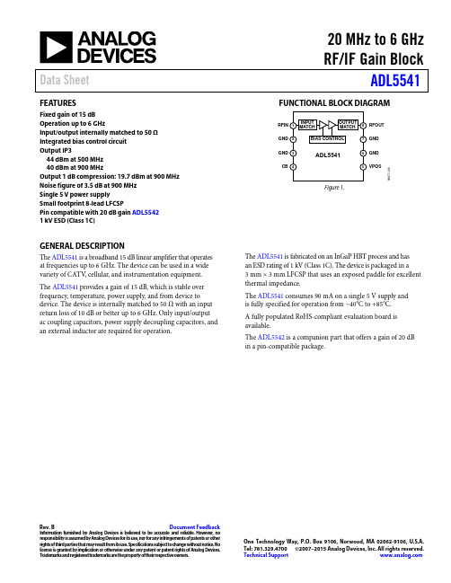
20 MHz to 6 GHzRF/IF Gain Block Data Sheet ADL5541FEATURESFixed gain of 15 dBOperation up to 6 GHzInput/output internally matched to 50 Ω Integrated bias control circuitOutput IP344 dBm at 500 MHz40 dBm at 900 MHzOutput 1 dB compression: 19.7 dBm at 900 MHz Noise figure of 3.5 dB at 900 MHzSingle 5 V power supplySmall footprint 8-lead LFCSPPin compatible with 20 dB gain ADL55421 kV ESD (Class 1C) FUNCTIONAL BLOCK DIAGRAMGNDRFOUTGNDVPOS6877-1Figure 1.GENERAL DESCRIPTIONThe ADL5541 is a broadband 15 dB linear amplifier that operates at frequencies up to 6 GHz. The device can be used in a wide variety of CATV, cellular, and instrumentation equipment. The ADL5541 provides a gain of 15 dB, which is stable over frequency, temperature, power supply, and from device to device. The device is internally matched to 50 Ω with an input return loss of 10 dB or better up to 6 GHz. Only input/output ac coupling capacitors, power supply decoupling capacitors, and an external inductor are required for operation. The ADL5541 is fabricated on an InGaP HBT process and has an ESD rating of 1 kV (Class 1C). The device is packaged in a3 mm × 3 mm LFCSP that uses an exposed paddle for excellent thermal impedance.The ADL5541 consumes 90 mA on a single 5 V supply andis fully specified for operation from −40°C to +85°C.A fully populated RoHS-compliant evaluation board is available.The ADL5542 is a companion part that offers a gain of 20 dB in a pin-compatible package.Rev. B Document Feedback Information furnished by Analog Devices is believed to be accurate and reliable. However, noresponsibility is assumed by Analog Devices for its use, nor for any infringements of patents or other rights of third parties that may result from its use. Specifications subject to change without notice. No license is granted by implication or otherwise under any patent or patent rights of Analog Devices. T rademarks and registered trademarks are the property of their respective owners. O ne Technology Way, P.O. Box 9106, Norwood, MA 02062-9106, U.S.A. Tel: 781.329.4700 ©2007–2015 Analog Devices, Inc. All rights reserved. Technical Support ADL5541 Data Sheet TABLE OF CONTENTSFeatures (1)Functional Block Diagram (1)General Description (1)Revision History (2)Specifications (3)Typical Scattering Parameters (5)Absolute Maximum Ratings (6)ESD Caution (6)Pin Configuration and Function Descriptions ............................. 7Typical Performance Characteristics . (8)Operating to 20 MHz (10)Basic Connections (11)Soldering Information and Recommended PCB Land Pattern (11)Evaluation Board (12)Outline Dimensions (13)Ordering Guide (13)REVISION HISTORY2/15—Rev. A to Rev. BChanged Frequency Range from 50 MHz to 6000 MHz to20 MHz to 6000 MHz (Throughout) (1)Changes to Table 1 (3)Added Figure 14 to Figure 19; Renumbered Sequentially (10)Changes to Basic Connections Section and Table 5; AddedFigure 21 and Figure 22 (11)Updated Outline Dimensions (13)Changes to Ordering Guide (13)11/13—Rev. 0 to Rev. AChanges to Figure 2 (7)Added Figure 13, Renumbered Sequentially (9)Added Exposed Pad Notation to Outline Dimensions (12)7/07—Revision 0: Initial VersionRev. B | Page 2 of 13Data Sheet ADL5541 SPECIFICATIONSVPOS = 5 V and T A = 25°C, unless otherwise noted.Table 1.Parameter Test Conditions/Comments Min Typ Max Unit OVERALL FUNCTIONFrequency Range 20 6000 MHz Gain (S21) 900 MHz 15.2 dB Input Return Loss (S11) Frequency 500 MHz to 5 GHz −12 dB Output Return Loss (S22) Frequency 500 MHz to 5 GHz −10 dB Reverse Isolation (S12) −19 dB FREQUENCY = 20 MHzGain 17.6 dB Output 1 dB Compression Point 18.3 dBm Output Third-Order Intercept Δf = 1 MHz, output power (P OUT) = 0 dBm per tone 38 dBm Noise Figure 3.3 dB FREQUENCY = 100 MHzGain 15.7 dB Output 1 dB Compression Point 19 dBm Output Third-Order Intercept Δf = 1 MHz, output power (P OUT) = 0 dBm per tone 37 dBm Noise Figure 3.9 dB FREQUENCY = 500 MHzGain 14.7 15.1 15.5 dB vs. Frequency ±50 MHz ±0.15 dB vs. Temperature −40°C ≤ T A ≤ +85°C ±0.1 dB vs. Supply 4.75 V to 5.25 V ±0.01 dB Output 1 dB Compression Point 19.9 dBm Output Third-Order Intercept Δf = 1 MHz, output power (P OUT) = 3 dBm per tone 44 dBm Noise Figure 3.5 3.7 dB FREQUENCY = 900 MHzGain 14.9 15.2 15.4 dB vs. Frequency ±50 MHz ±0.03 dB vs. Temperature −40°C ≤ T A ≤ +85°C ±0.15 dB vs. Supply 4.75 V to 5.25 V ±0.01 dB Output 1 dB Compression Point 19.7 dBm Output Third-Order Intercept Δf = 1 MHz, output power (P OUT) = 0 dBm per tone 40.8 dBm Noise Figure 3.5 3.7 dB FREQUENCY = 2000 MHzGain 13.9 14.7 15.4 dB vs. Frequency ±50 MHz ±0.03 dB vs. Temperature −40°C ≤ T A ≤ +85°C ±0.17 dB vs. Supply 4.75 V to 5.25 V ±0.01 dB Output 1 dB Compression Point 16.3 dBm Output Third-Order Intercept Δf = 1 MHz, output power (P OUT) = 0 dBm per tone 39.2 dBm Noise Figure 3.8 4.0 dB FREQUENCY = 2400 MHzGain 13.9 14.5 15.1 dB vs. Frequency ±50 MHz ±0.03 dB vs. Temperature −40°C ≤ T A ≤ +85°C ±0.19 dB vs. Supply 4.75 V to 5.25 V ±0.02 dB Output 1 dB Compression Point 14.9 dBm Output Third-Order Intercept Δf = 1 MHz, output power (P OUT) = 0 dBm per tone 38.6 dBm Noise Figure 4.0 4.2 dBRev. B | Page 3 of 13ADL5541 Data Sheet Parameter Test Conditions/Comments Min Typ Max Unit FREQUENCY = 3500 MHzGain 13.6 14.3 14.9 dB vs. Frequency ±50 MHz ±0.03 dB vs. Temperature −40°C ≤ T A ≤ +85°C ±0.19 dB vs. Supply 4.75 V to 5.25 V ±0.02 dB Output 1 dB Compression Point 12.1 dBm Output Third-Order Intercept Δf = 1 MHz, output power (P OUT) = 0 dBm per tone 30.7 dBm Noise Figure 4.2 4.5 dB FREQUENCY = 5800 MHzGain 9.1 11.2 13.5 dB vs. Frequency ±50 MHz ±0.15 dB vs. Temperature −40°C ≤ T A ≤ +85°C ±0.9 dB vs. Supply 4.75 V to 5.25 V ±0.02 dB Output 1 dB Compression Point 5.8 dBm Output Third-Order Intercept Δf = 1 MHz, output power (P OUT) = 0 dBm per tone 21.9 dBm Noise Figure 6.0 7.0 dB POWER INTERFACE Pin VPOSSupply Voltage (VPOS) 4.5 5 5.5 V Supply Current 90 100 mA vs. Temperature −40°C ≤ T A ≤ +85°C ±12 mA Power Dissipation VPOS = 5 V 0.5 WRev. B | Page 4 of 13Data Sheet ADL5541TYPICAL SCATTERING PARAMETERSVPOS = 5 V and T A = 25°C, the effects of the test fixture have been de-embedded up to the pins of the device.Table 2.Freq. (MHz)S11 S21 S12 S22 Magnitude (dB) Angle (°) Magnitude (dB) Angle (°)Magnitude (dB) Angle (°)Magnitude (dB) Angle (°)50 −18.11 −134.53 16.29 +166.36 −19.15 +3.84 −17.89 −134.08 100 −20.84 −161.29 15.93 +168.53 −18.82 +2.26 −22.24 −155.22 500 −27.69 +115.36 15.58 +154.53 −18.70 −13.59 −24.96 +176.64 900 −27.48 +101.79 15.52 +136.22 −18.70 −26.33 −22.38 +173.92 1000 −26.87 +91.91 15.56 +131.64 −18.64 −29.43 −23.15 +174.28 1500 −29.18 −107.74 15.50 +108.03 −18.64 −44.69 −19.35 +167.80 2000 −17.88 −153.68 15.51 +84.72 −18.43 −60.42 −14.13 +176.19 2500 −9.87 +169.30 15.57 +59.74 −18.32 −75.48 −9.89 +161.55 3000 −7.92 +142.75 15.49 +35.05 −17.93 −92.29 −8.69 +138.18 3500 −7.74 +117.57 15.21 +9.15 −18.14 −110.62 −11.02 +100.39 4000 −10.85 +116.84 14.82 −16.13 −18.11 −125.08 −15.70 +6.37 4500 −13.25 +136.93 15.23 −41.75 −17.54 −142.99 −7.83 −80.59 5000 −13.97 +143.02 14.56 −68.15 −17.64 −161.24 −6.87 −112.39 5500 −13.68 −121.08 13.89 −96.10 −17.47 +178.77 −11.66 −102.32 6000 −4.52 −138.62 12.07 −123.56 −18.61 +157.35 −7.66 −54.40Rev. B | Page 5 of 13ADL5541 Data Sheet ABSOLUTE MAXIMUM RATINGSESD CAUTIONTable 3.Parameter RatingSupply Voltage, VPOS 6.5 VInput Power (re: 50 Ω)10 dBmInternal Power Dissipation (Paddle Soldered) 650 mWθJC (Junction to Paddle)28.5°C/WMaximum Junction Temperature 150°COperating Temperature Range −40°C to +85°CStorage Temperature Range −65°C to +150°CStresses at or above those listed under Absolute MaximumRatings may cause permanent damage to the product. This is astress rating only; functional operation of the product at theseor any other conditions above those indicated in the operationalsection of this specification is not implied. Operation beyondthe maximum operating conditions for extended periods mayaffect product reliability.Rev. B | Page 6 of 13Data SheetADL5541PIN CONFIGURATION AND FUNCTION DESCRIPTIONS06877-002GND CB RFIN NOTES1. EXPOSED PADDLE. INTERNALLY CONNECTED TO GND. SOLDER TO A LOW IMPEDANCE GROUND PLANE.GND GND VPOSRFOUT GNDFigure 2. Pin ConfigurationTable 4. Pin Function DescriptionsPin No. Mnemonic Description1RFIN RF Input. Requires a dc blocking capacitor.2, 3, 6, 7 GND Ground. Connect these pins to a low impedance ground plane.4 CB Low Frequency Bypass. A 1 µF capacitor should be connected between this pin and ground.5 VPOS Power Supply for Bias Controller. Connect directly to external power supply.8RFOUT RF Output and Supply Voltage. DC bias is provided to this pin through an inductor that is tied to the external power supply. RF path requires a dc blocking capacitor.Exposed PaddleExposed Paddle. Internally connected to GND. Solder to a low impedance ground plane.Rev. B | Page 7 of 13ADL5541Data SheetRev. B | Page 8 of 13TYPICAL PERFORMANCE CHARACTERISTICSVPOS = 5 V and T A = 25°C, unless otherwise noted. C1 = 33 pF, C2 = 33 pF, L1 = 47 nH.45FREQUENCY (GHz)G A I N , P 1d B , O I P 3, N F (d B , d B m )403530252015105.75.34.94.54.13.73.32.92.52.11.71.30.90.506877-003Figure 3. Gain, P1dB, OIP3, and Noise Figure vs. Frequency1610FREQUENCY (GHz)G A I N (d B )5.75.34.94.54.13.73.32.92.52.11.71.30.90.5151413121106877-004Figure 4. Gain vs. Frequency and Temperature–4506FREQUENCY (GHz)S 11, S 22, S 12 (d B )–5–10–15–20–25–30–35–401234506877-005Figure 5. Input Return Loss (S11), Output Return Loss (S22), andReverse Isolation (S12) vs. Frequency450FREQUENCY (GHz)O I P 3 A ND P 1d B (d B m )4035302520151055.75.34.94.54.13.73.32.92.52.11.71.30.90.5Figure 6. OIP3 and P1dB vs. Frequency and Temperature5010–515P OUT (dBm)O I P 3 (d B m )45403530252015–3–1135791113Figure 7. OIP3 vs. Output Power (P OUT ) and Frequency820 6.0FREQUENCY (GHz)N O I S E F I G U R E (d B )765430.5 1.0 1.5 2.0 2.5 3.0 3.5 4.0 4.5 5.0 5.5Figure 8. Noise Figure vs. Frequency and TemperatureData SheetADL55413037.0OIP3 (dBm)P E R C E N T A G E (%)25201510538.540.041.543.006877-009Figure 9. OIP3 Distribution at 900 MHz2519.4P1dB (dBm)P E R C E N T A G E (%)201510519.519.619.719.819.920.020.106877-010Figure 10. P1dB Distribution at 900 MHz2515.08GAIN (dB)P E R C E N T A G E (%)201510515.1115.1415.1715.2015.2315.2606877-011Figure 11. Gain Distribution at 900 MHz3003.303.36 3.42 3.48 3.54 3.60 3.66 3.72 3.78NOISE FIGURE (dB)P E R C E N T A G E (%)252015105Figure 12. Noise Figure Distribution at 900 MHz100707580859095–6–4–2024681012141618202206877-100S U P P L Y C U R R EN T (m A )P OUT (dBm)Figure 13. Supply Current vs. P OUT and TemperatureRev. B | Page 9 of 13ADL5541Data SheetOPERATING TO 20 MHzVPOS = 5 V and T A = 25°C, unless otherwise noted. C1 = 0.1 µF, C2 = 0.1 µF, L1 = 1 µH.0510********354020406080100120140G A I N , P 1d B , O I P 3, N F (d B , d B m )FREQUENCY (MHz)06877-114Figure 14. Gain, P1dB, OIP3, and Noise Figure vs. Frequency15.015.516.016.517.017.518.020406080100120140G AI N (d B )FREQUENCY (MHz)06877-115Figure 15. Gain vs. Frequency and Temperature–30–25–20–15–10–52030405060708090100110120130140S 11,S 22, S 12 (d B )FREQUENCY (MHz)06877-116Figure 16. Input Return Loss (S11), Output Return Loss (S22), andReverse Isolation (S12) vs. Frequency51015202530354045O I P 3A N D P 1d B (d B m )FREQUENCY (MHz)06877-117Figure 17. OIP3 and P1dB vs. Frequency and Temperature2022242628303234363840–5–3–11357911131506877-118O I P 3 (d B m )P OUT (dBm)Figure 18. OIP3 vs. Output Power (P OUT ) and Frequency2.02.53.03.54.04.55.020406080100120140N O I S E F I G U R E (d B )FREQUENCY (MHz)+25°C–40°C+85°C06877-119Figure 19. Noise Figure vs. Frequency and TemperatureRev. B | Page 10 of 13Data SheetADL5541BASIC CONNECTIONSThe basic connections for operating the ADL5541 are shown in Figure 20. Recommended components are listed in Table 5. The input and output should be ac-coupled with appropriately sized capacitors (device characterization was performed with 33 pF capacitors). A 5 V dc bias is supplied to the amplifier via GND (Pin 6) and through a biasing inductor connected to RFOUT (Pin 8). The bias voltage should be decoupled using a 1 µFRFIN RFOUT06877-013Figure 20. Basic ConnectionsFor operation below 500 MHz, a larger biasing choke and ac coupling capacitors are necessary (see Table 5). Figure 21 shows input return loss, output return loss, and gain for frequencies between 200 MHz and 500 MHz. The noise figure performance for operation from 200 MHz to 500 MHz is shown in Figure 22.–30–25–20–15–10–512.012.513.013.514.014.515.015.516.016.517.0200250300350400450500R E T U R N L O S S (d B )G A I N (d B )FREQUENCY (MHz)06877-121Figure 21. Input Return Loss (S11), Output Return Loss (S22), andGain (S21) vs. Frequency2.02.53.03.54.04.5200250300350400450500N O I S E F I G U R E (d B )FREQUENCY (MHz)06877-122Figure 22. Noise Figure vs. Frequency from 200 MHz to 500 MHzSOLDERING INFORMATION AND RECOMMENDED PCB LAND PATTERNFigure 23 shows the recommended land pattern for the ADL5541. To minimize thermal impedance, the exposed paddle on the package underside should be soldered down to a ground plane along with Pin 2, Pin 3, Pin 6, and Pin 7. If multiple ground layers exist, they should be stitched together using vias (aminimum of five vias is recommended). For more information on land pattern design and layout, refer to Application Note AN-772, A Design and Manufacturing Guide for the Lead Frame 06877-016Figure 23. Recommended Land PatternTable 5. Recommended Components for Basic ConnectionsFrequencyC1 C2 C3 L1C4 C5 C6 C7 20 MHz to 200 MHz 0.1 µF 0.1 µF 1 µF 1 µH (Coilcraft 0805LS-102XJL_ or equivalent) 68 pF 1.2 nF 1 µF 68 pF 200 MHz to 500 MHz 0.1 µF 0.1 µF 1 µF 470 nH (Coilcraft 0603LS-471-NX or equivalent) 68 pF 1.2 nF 1 µF 68 pF 500 MHz to 6000 MHz33 pF33 pF1 µF47 nH (Coilcraft 0603CS-47-NX or equivalent)68 pF1.2 nF1 µF68 pFRev. B | Page 11 of 13ADL5541Data SheetRev. B | Page 12 of 13EVALUATION BOARDFigure 26 shows the schematic for the ADL5541 evaluation board. The board is powered by a single 5 V supply.The components used on the board are listed in Table 6. Power can be applied to the board through clip-on leads (VCC and GND) or through a 2-pin header (W1).06877-017Figure 24. Evaluation Board Layout (Bottom)06877-018Figure 25. Evaluation Board Layout (Top)RFIN06877-019Figure 26. Evaluation Board SchematicTable 6. Evaluation Board ConfigurationComponent Fun c tion Default ValueDUT1 Gain block ADL5541 C1, C2 AC coupling capacitors 33 pF, 0402 C3 Low frequency bypass capacitor 1 μF, 0805C4, C5, C6, C7, C8, C9 Power supply decoupling capacitors C4 and C7 = 68 pF, 0603 C5 = 1.2 nF, 0603 C6 = 1 μF, 0805 C8 and C9 = openL1 DC bias inductor 47 nH, 0603 (Coilcraft 0603CS-47-NX or equivalent) VCC and GND Clip-on terminals for power supply W1 2-pin header for connection of ground and supply via cableData SheetADL5541Rev. B | Page 13 of 13OUTLINE DIMENSIONSPIN 10.80FOR PROPER CONNECTION OF THE EXPOSED PAD,REFER TO THE PIN CONFIGURATION AND FUNCTION DESCRIPTIONSSECTION OF THIS DATA SHEET.0.08COMPLIANT TO JEDEC STANDARDS MO-229-WEED12-07-2010-AFigure 27. 8-Lead Lead Frame Chip Scale Package [LFCSP_WD]3 mm × 3 mm Body, Very Very Thin, Dual Lead(CP-8-13)Dimensions shown in millimetersORDERING GUIDEModel 1 Temperature Range Package DescriptionPackage OptionBranding ADL5541ACPZ-R7 −40°C to +85°C 8-Lead LFCSP_WD, 7” Tape and Reel CP-8-13 Q13 ADL5541-EVALZEvaluation Board1Z = RoHS Compliant Part.©2007–2015 Analog Devices, Inc. All rights reserved. Trademarks and registered trademarks are the property of their respec tive owners. D06877-0-2/15(B)。
西门子电机参数
选型技术数据表 Technical data table ............................................................. 22
■ Available in 2, 4, 6 pole variants with efficiency grade 2. according to GB18613-2006 and efficiency class IE2 according to IEC 60034-30.
■ 额定功率:0.55 kW ~ 315 kW(50 Hz);
■ Insulation system is designed for temperature class 155 (F). At rated output with line-fed operation, the motors can be used in temperature class 130 (B).
Padm = Prated • kHT
对于不同高度和(或)不同环境温度的功率换算系数 kHT Factor kHT for different side altitudes and / or coolant temperature
海拔高度 Site altitude above see level
对应海拔高度的环境温度 Site altitude above see level Coolant temperature
55 ºC 0.87 0.84 0.82 0.78 0.75 0.71 0.67
- 1、下载文档前请自行甄别文档内容的完整性,平台不提供额外的编辑、内容补充、找答案等附加服务。
- 2、"仅部分预览"的文档,不可在线预览部分如存在完整性等问题,可反馈申请退款(可完整预览的文档不适用该条件!)。
- 3、如文档侵犯您的权益,请联系客服反馈,我们会尽快为您处理(人工客服工作时间:9:00-18:30)。
Downloaded from by on April 14, 2008
Circulation Research
An Otticiui Journal of the American Heart Association
DECEMBER VOL. 39
The online version of this article, along with updated information and services, is located on the World Wide Web at:
ቤተ መጻሕፍቲ ባይዱ
Subscriptions: Information about subscribing to Circulation Research is online at /subscriptions/ Permissions: Permissions & Rights Desk, Lippincott Williams & Wilkins, a division of Wolters Kluwer Health, 351 West Camden Street, Baltimore, MD 21202-2436. Phone: 410-528-4050. Fax: 410-528-8550. E-mail: journalpermissions@ Reprints: Information about reprints can be found online at /reprints
1976 NO. 6
Automatic Activity in Depolarized Guinea Pig Ventricular Myocardium
Characteristics and Mechanisms
SUNAO IMANISHI, M . D . , AND BORYS SURAWICZ, M . D .
AUTOMATICITY of ventricular myocardial fibers has been observed after supervision with K+-free and Ca2+free solution,1 exposure to Ba2+ salts,1' 3 excessive mechanical stretch,4 and several other interventions (for references, see Antoni5 and Cranefield,6 p. 213). Common to all these interventions is the depolarization to levels of membrane potential at which the rapid inward sodium current is partly or completely inactivated. Automatic activity of ventricular myocardium also has been induced by depolarizing direct current pulses of several seconds' duration applied across a single sucrose gap in sodiumfree7 and regular Tyrode's solution .e- • Recently Katzung8'9 showed that Ca and Na ions influence automaticity of papillary muscles from guinea pigs and cats and dog trabeculae after depolarizations to membrane potentials less negative than —60 mV. Imanishi10 used the partition chamber method of Kamiyama and Matsuda" to study the effect of depolarizing currents on quiescent dog Purkinje fibers. In this preparation depolarization induced CaI+-sensitive oscillations
Circulation Research is published by the American Heart Association. 7272 Greenville Avenue, Dallas, TX 72514 Copyright © 1976 American Heart Association. All rights reserved. Print ISSN: 0009-7330. Online ISSN: 1524-4571
Automatic activity in depolarized guinea pig ventricular myocardium. Characteristics and mechanisms S Imanishi and B Surawicz Circ. Res. 1976;39;751-759
SUMMARY Membrane potential was changed uniformly in segments, 0.7-1.0 mm long, of guinea pig papillary muscles exdsed from the right ventricle by using extracellular polarizing current pulses applied across two electrically insulated compartments. Rhythmic automatic depolarizations (RAD) occurred in 90% of preparations superfused with Tyrode's solution at maximum dlastolic membrane potentials ranging from - 3 5 . 2 ± 7.5 (threshold) to +4.0 ± 9.2 mV. The average maximum dV/dt of RAD ranged from 17.1 to 18.0 V/sec within a membrane potential range of - 4 0 to +20 mV. Raising extracellular Ca'+ concentration [Ca1+]n from 1.8 to 6.8 ITIM, or application of isoproterenol (10-* g/ml) enhanced the rate of RAD, but lowering |Ca J+ ],, to 0.4 iuM or exposure to MnCl, (6 mix) abolished RAD. RAD
From the Cardiovascular Division, Department of Medicine, Univenity of Kentucky Medical Center, Lexington, Kentucky. Supported by NIHL Training Grant 203-60-7H350-A3BB6 and a grant from the Kentucky Heart Association. Dr. Imanishi is a Research Fellow of the Kentucky Heart Association. Address for reprints: Borys Surawicz, M.D., Department of Medicine, University of Kentucky Medical Center, Lexington, Kentucky 40506. Original manuscript received May 1975; accepted for publication July 15, 1976.
were enhanced by lowering extracellular K+ concentration | K + ] 0 from 5.4 to 1.5 DIM. RAD were suppressed in 40% of fibers by raising [K+]n to 15.4 raM, and hi all fibers by raising [K+]o to 40.4 HIM. This suppression was dne to increased |K + ],, and not to Kinduced depolarization because it persisted when membrane potential was held by means of a conditioning hyperpolarizing pulse at the level of control resting potential. The slope resistance increased gradually after maximum re polarization. These observations suggest that the development of RAD in depolarized myocardium is associated with a time-dependent decrease in outward current (probably K current) and with increase in the background inward current, presumably flowing through the stow channel carrying Ca or Na ions, or both.