TC4421A中文数据手册(Microchip)「EasyDatasheet」
TC4427COA713;TC4427COA;TC4428COA;TC4426COA;TC4428EOA;中文规格书,Datasheet资料
DS21422D-page 2
/
© 2006 Microchip Technology Inc.
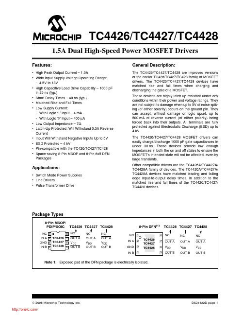
TC4426/TC4427/TC4428
1.0 ELECTRICAL CHARACTERISTICS
Absolute Maximum Ratings †
VDD = 18V
Rise Time Fall Time Delay Time Delay Time Power Supply
tR
—
19 30 ns Figure 4-1
tF
—
19 30 ns Figure 4-1
tD1
—
20 30 ns Figure 4-1
tD2
—
40 50 ns Figure 4-1
Electrical Specifications: Unless otherwise noted, TA = +25ºC with 4.5V ≤ VDD ≤ 18V.
Parameters
Sym
Min
Typ Max Units
Conditions
Input
Logic ‘1’, High Input Voltage
Supply Voltage ..................................................... +22V
Input Voltage, IN A or IN B ..................................... (VDD + 0.3V) to (GND – 5V)
Package Power Dissipation (TA ≤ 70°C) DFN .............................................................. Note 3 MSOP .......................................................... 340 mW PDIP ............................................................ 730 mW SOIC............................................................ 470 mW
TC4423 datasheet

- With Logic ‘1’ Input – 3.5 mA (Max) - With Logic ‘0’ Input – 350 µA (Max) • Low Output Impedance: 3.5Ω (typ) • Latch-Up Protected: Will Withstand 1.5A Reverse Current • Logic Input Will Withstand Negative Swing Up To 5V • ESD Protected: 4 kV • Pin compatible with the TC1426/TC1427/TC1428, TC4426/TC4427/TC4428 and TC4426A/ TC4427A/TC4428A devices. • Space-saving 8-Pin 6x5 DFN Package
(Each Input)
GND
Non-inverting
4.7V TC4423 Dual Inverting TC4424 Dual Non-inverting TC4425 One Inverting, One Non-inverting
Note 1: Unused inputs should be grounded.
16-Pin SOIC (Wide) TC4423 TC4424 TC4425
NC 1 IN A 2 NC 3 GND 4 GND 5 NC 6 IN B 7 NC 8
TC4423 TC4424 TC4425
TC4420VG资料

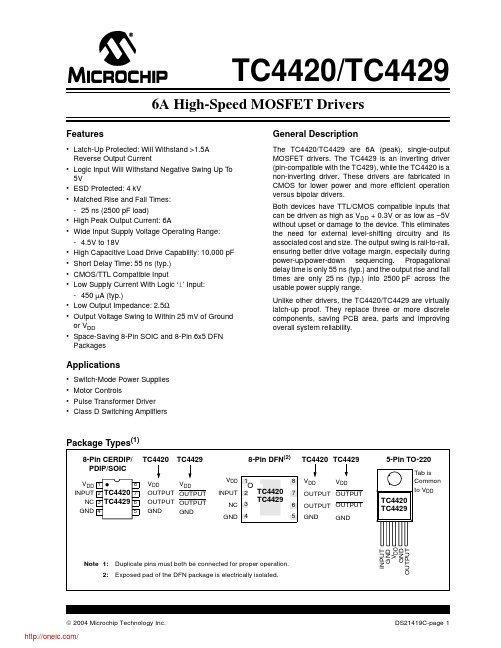
2004 Microchip Technology Inc.DS21419C-page 1TC4420/TC4429Features•Latch-Up Protected: Will Withstand >1.5A Reverse Output Current•Logic Input Will Withstand Negative Swing Up To 5V•ESD Protected: 4kV•Matched Rise and Fall Times:-25ns (2500pF load)•High Peak Output Current: 6A•Wide Input Supply Voltage Operating Range:- 4.5V to 18V•High Capacitive Load Drive Capability: 10,000pF •Short Delay Time: 55ns (typ.)•CMOS/TTL Compatible Input•Low Supply Current With Logic ‘1’ Input:-450µA (typ.)•Low Output Impedance: 2.5Ω•Output Voltage Swing to Within 25mV of Ground or V DD•Space-Saving 8-Pin SOIC and 8-Pin 6x5 DFN PackagesApplications•Switch-Mode Power Supplies •Motor Controls•Pulse Transformer Driver •Class D Switching AmplifiersGeneral DescriptionThe TC4420/TC4429 are 6A (peak), single-output MOSFET drivers. The TC4429 is an inverting driver (pin-compatible with the TC429), while the TC4420 is a non-inverting driver. These drivers are fabricated in CMOS for lower power and more efficient operation versus bipolar drivers.Both devices have TTL/CMOS compatible inputs that can be driven as high as V DD + 0.3V or as low as –5V without upset or damage to the device. This eliminates the need for external level-shifting circuitry and its associated cost and size. The output swing is rail-to-rail,ensuring better drive voltage margin, especially during power-up/power-down sequencing. Propagational delay time is only 55ns (typ.) and the output rise and fall times are only 25ns (typ.) into 2500pF across the usable power supply range.Unlike other drivers, the TC4420/TC4429 are virtually latch-up proof. They replace three or more discrete components, saving PCB area, parts and improving overall system reliability.Package Types (1)5-Pin TO-220V D D G N D I N P U T G N D O U T P U TTC4420TC4429Tab is Common to V DD8-Pin CERDIP/1234V DD5678OUTPUT GNDV DD INPUTNC GNDOUTPUT TC4420TC4429TC4420TC4429V DDOUTPUT GNDOUTPUT PDIP/SOICNote 1:Duplicate pins must both be connected for proper operation.2:Exposed pad of the DFN package is electrically isolated.8-Pin DFN (2)V DD INPUT NC GND 23456781TC4420TC4429V DDOUTPUT GNDOUTPUT TC4420TC4429V DDOUTPUT GNDOUTPUT 6A High-Speed MOSFET DriversTC4420/TC4429DS21419C-page 2 2004 Microchip Technology Inc.Functional Block DiagramEffective Input TC4420OutputInputGNDV DD300mV4.7VC = 38pFTC4429500µA Non-InvertingInvertingTC4420/TC44291.0ELECTRICALCHARACTERISTICSAbsolute Maximum Ratings†Supply Voltage.....................................................+20V Input Voltage..................................– 5V to V DD + 0.3V Input Current (V IN > V DD)...................................50mA Power Dissipation (T A≤ 70°C)5-Pin TO-220....................................................1.6W CERDIP.......................................................800mW DFN...............................................................Note2 PDIP............................................................730mW SOIC............................................................470mW Package Power Dissipation (T A≤ 25°C)5-Pin TO-220 (With Heatsink)........................12.5W Thermal Impedances (To Case)5-Pin TO-220 RθJ-C......................................10°C/W † Stresses above those listed under “Absolute Maximum Ratings” may cause permanent damage to the device. These are stress ratings only and functional operation of the device at these or any other conditions above those indicated in the operation sections of the specifications is not implied. Exposure to Absolute Maximum Rating conditions for extended periods may affect device reliability.DC CHARACTERISTICSElectrical Specifications: Unless otherwise noted, T A = +25°C with 4.5V ≤ V DD≤ 18V.Parameters Sym Min Typ Max Units ConditionsInputLogic ‘1’, High InputVoltageV IH 2.4 1.8—VLogic ‘0’, Low Input Voltage V IL— 1.30.8VInput Voltage Range V IN–5—V DD+0.3VInput Current I IN–10—+10µA0V ≤ V IN ≤ V DDOutputHigh Output Voltage V OH V DD – 0.025——V DC TESTLow Output Voltage V OL——0.025V DC TESTOutput Resistance, High R OH— 2.1 2.8ΩI OUT = 10mA, V DD = 18V Output Resistance, Low R OL— 1.5 2.5ΩI OUT = 10mA, V DD = 18V Peak Output Current I PK— 6.0—A V DD = 18VLatch-Up ProtectionWithstand Reverse CurrentI REV—> 1.5—A Duty cycle ≤ 2%, t ≤ 300µsec Switching Time(Note1)Rise Time t R—2535ns Figure4-1, C L = 2,500pF Fall Time t F—2535ns Figure4-1, C L = 2,500pF Delay Time t D1—5575ns Figure4-1Delay Time t D2—5575ns Figure4-1Power SupplyPower Supply Current I S——0.45551.5150mAµAV IN = 3VV IN = 0VOperating Input Voltage V DD 4.5—18VNote1:Switching times ensured by design.2:Package power dissipation is dependent on the copper pad area on the PCB.2004 Microchip Technology Inc.DS21419C-page 3TC4420/TC4429DS21419C-page 4 2004 Microchip Technology Inc.DC CHARACTERISTICS (OVER OPERATING TEMPERATURE RANGE)TEMPERATURE CHARACTERISTICSElectrical Specifications: Unless otherwise noted, over operating temperature range with 4.5V ≤ V DD ≤ 18V.ParametersSymMinTypMaxUnitsConditionsInputLogic ‘1’, High Input VoltageV IH 2.4——V Logic ‘0’, Low Input Voltage V IL ——0.8V Input Voltage Range V IN –5—V DD + 0.3V Input Current I IN–10—+10µA0V ≤ V IN ≤ V DDOutputHigh Output Voltage V OH V DD – 0.025——V DC TEST Low Output Voltage V OL ——0.025V DC TESTOutput Resistance, High R OH —35ΩI OUT = 10mA, V DD = 18V Output Resistance, Low R OL—2.35ΩI OUT = 10mA, V DD = 18VSwitching Time (Note 1)Rise Time t R —3260ns Figure 4-1, C L = 2,500pF Fall Time t F —3460ns Figure 4-1, C L = 2,500pF Delay Time t D1—50100ns Figure 4-1Delay Time t D2—65100nsFigure 4-1Power Supply Power Supply Current I S ——0.45603400mA µA V IN = 3V V IN = 0VOperating Input Voltage V DD4.5—18VNote 1:Switching times ensured by design.Electrical Specifications: Unless otherwise noted, all parameters apply with 4.5V ≤ V DD ≤ 18V.ParametersSymMinTypMaxUnitsConditionsTemperature RangesSpecified Temperature Range (C)T A 0—+70°C Specified Temperature Range (I)T A –25—+85°C Specified Temperature Range (E)T A –40—+85°C Specified Temperature Range (V)T A –40—+125°C Maximum Junction Temperature T J ——+150°C Storage Temperature Range T A–65—+150°CPackage Thermal Resistances Thermal Resistance, 5L-TO-220θJA —71—°C/W Thermal Resistance, 8L-CERDIP θJA —150—°C/W Thermal Resistance, 8L-6x5 DFN θJA —33.2—°C/W Typical four-layer board with vias to ground plane.Thermal Resistance, 8L-PDIP θJA —125—°C/W Thermal Resistance, 8L-SOICθJA—155—°C/WTC4420/TC4429 2.0TYPICAL PERFORMANCE CURVESNote: Unless otherwise indicated, T A = +25°C with 4.5V ≤ V DD≤ 18V.FIGURE 2-1:Rise Time vs. Supply Voltage.FIGURE 2-2:Rise Time vs. Capacitive Load.FIGURE 2-3:Propagation Delay Time vs. Temperature.FIGURE 2-4:Fall Time vs. Supply Voltage.FIGURE 2-5:Fall Time vs. Capacitive Load.FIGURE 2-6:Supply Current vs. Capacitive Load.Note:The graphs and tables provided following this note are a statistical summary based on a limited number of samples and are provided for informational purposes only. The performance characteristics listed herein are not tested or guaranteed. In some graphs or tables, the data presented may be outside the specified operating range (e.g., outside specified power supply range) and therefore outside the warranted range.2004 Microchip Technology Inc.DS21419C-page 5TC4420/TC4429DS21419C-page 6 2004 Microchip Technology Inc.Note: Unless otherwise indicated, T A = +25°C with 4.5V ≤ V DD ≤ 18V.FIGURE 2-7:Rise and Fall Times vs.Temperature.FIGURE 2-8:Propagation Delay Time vs.Supply Voltage.FIGURE 2-9:Supply Current vs.Frequency.FIGURE 2-10:High-State Output Resistance vs Supply Voltage.FIGURE 2-11:Effect of Input Amplitude on Propagation Delay.FIGURE 2-12:Low-State Output Resistance vs. Supply Voltage.TC4420/TC4429 Note: Unless otherwise indicated, T A = +25°C with 4.5V ≤ V DD≤ 18V.FIGURE 2-13:Crossover Energy.2004 Microchip Technology Inc.DS21419C-page 7TC4420/TC4429DS21419C-page 8 2004 Microchip Technology Inc.3.0PIN DESCRIPTIONSThe descriptions of the pins are listed in Table 3-1.TABLE 3-1:PIN FUNCTION TABLE3.1Supply Input (V DD )The V DD input is the bias supply for the MOSFET driver and is rated for 4.5V to 18V with respect to the ground pins. The V DD input should be bypassed to ground with a local ceramic capacitor. The value of the capacitor should be chosen based on the capacitive load that is being driven. A minimum value of 1.0µF is suggested.3.2Control InputThe MOSFET driver input is a high-impedance,TTL/CMOS compatible input. The input circuitry of the TC4420/TC4429 MOSFET driver also has a “speed-up” capacitor. This helps to decrease the propagation delay times of the driver. Because of this, input signals with slow rising or falling edges should not be used, as this can result in double-pulsing of the MOSFET driver output.3.3CMOS Push-Pull OutputThe MOSFET driver output is a low-impedance,CMOS, push-pull style output capable of driving a capacitive load with 6.0A peak currents. The MOSFET driver output is capable of withstanding 1.5A peak reverse currents of either polarity.3.4GroundThe ground pins are the return path for the bias current and the high peak currents that discharge the load capacitor. The ground pins should be tied into a ground plane or have very short traces to the bias supply source return.3.5Exposed Metal PadThe exposed metal pad of the 6x5 DFN package is not internally connected to any potential. Therefore, this pad can be connected to a ground plane or other copper plane on a printed circuit board (PCB) to aid in heat removal from the package.Pin No.8-Pin CERDIP/ PDIP/SOICPin No.8-Pin DFNPin No.5-Pin TO-220SymbolDescription11—V DD Supply input, 4.5V to 18V221INPUT Control input, TTL/CMOS compatible input 33—NC No Connection 442GND Ground 554GND Ground665OUTPUT CMOS push-pull output 77—OUTPUT CMOS push-pull output 883V DD Supply input, 4.5V to 18V —PAD —NC Exposed MetalPad ——TABV DDMetal Tab is at the V DD Potential2004 Microchip Technology Inc.DS21419C-page 9TC4420/TC44294.0APPLICATIONS INFORMATIONFIGURE 4-1:Switching Time Test Circuits.Inverting DriverNon-Inverting DriverInputt D1t Ft Rt D2Input: 100kHz,square wave,t RISE = t FALL ≤ 10nsOutputInputOutputt D1t Ft Rt D2+5V 10%90%10%90%10%90%+18V 0V90%10%10%10%90%+5V +18V0V0V 0V 90%2675418C L = 2,500pF0.1µF4.7µFInputV DD = 18VOutput0.1µF Note: Pinout shown is for the PDIP , SOIC, DFN and CERDIP packages.TC4429TC4420TC4420/TC4429DS21419C-page 10 2004 Microchip Technology Inc.5.0PACKAGING INFORMATION5.1Package Marking InformationLegend: XX (X)Customer specific information*YY Year code (last 2 digits of calendar year)WW Week code (week of January 1 is week ‘01’)NNN Alphanumeric traceability codeNote :In the event the full Microchip part number cannot be marked on one line, it will be carried over to the next line thus limiting the number of available characters for customer specific information.*Standard OTP marking consists of Microchip part number, year code, week code, and traceability code.5-Lead TO-220Example:8-Lead CERDIP (300 mil)Example:8-Lead DFNExample :2004 Microchip Technology Inc.DS21419C-page 11TC4420/TC4429Package Marking Information (Continued)8-Lead PDIP (300 mil)Example:8-Lead SOIC (150 mil)Example:TC4420/TC4429DS21419C-page 12 2004 Microchip Technology Inc.TC4420/TC4429 8-Lead Ceramic Dual In-line – 300 mil (JA) (CERDIP)2004 Microchip Technology Inc.DS21419C-page 13TC4420/TC4429DS21419C-page 14 2004 Microchip Technology Inc.2004 Microchip Technology Inc.DS21419C-page 15TC4420/TC44298-Lead Plastic Dual In-line (PA) – 300 mil (PDIP)B1BA1ALA2pαEeBβcE1nD12UnitsINCHES*MILLIMETERSDimension LimitsMINNOMMAXMIN NOMMAXNumber of Pins n 88Pitchp.100 2.54Top to Seating PlaneA .140.155.170 3.56 3.94 4.32Molded Package Thickness A2.115.130.145 2.92 3.30 3.68Base to Seating PlaneA1.0150.38Shoulder to Shoulder Width E .300.313.3257.627.948.26Molded Package Width E1.240.250.260 6.10 6.35 6.60Overall LengthD .360.373.3859.149.469.78Tip to Seating Plane L .125.130.135 3.18 3.30 3.43Lead Thickness c .008.012.0150.200.290.38Upper Lead Width B1.045.058.070 1.14 1.46 1.78Lower Lead Width B .014.018.0220.360.460.56Overall Row Spacing §eB .310.370.4307.879.4010.92Mold Draft Angle Top α5101551015Mold Draft Angle Bottom β5101551015* Controlling Parameter Notes:Dimensions D and E1 do not include mold flash or protrusions. Mold flash or protrusions shall not exceed JEDEC Equivalent: MS-001Drawing No. C04-018.010” (0.254mm) per side.§ Significant CharacteristicTC4420/TC4429DS21419C-page 16 2004 Microchip Technology Inc.8-Lead Plastic Small Outline (OA) –Narrow, 150 mil (SOIC)Foot Angleφ048048151201512βMold Draft Angle Bottom 1512015120αMold Draft Angle Top 0.510.420.33.020.017.013B Lead Width0.250.230.20.010.009.008c Lead Thickness 0.760.620.48.030.025.019L Foot Length 0.510.380.25.020.015.010h Chamfer Distance 5.004.904.80.197.193.189D Overall Length 3.993.913.71.157.154.146E1Molded Package Width 6.206.025.79.244.237.228E Overall Width0.250.180.10.010.007.004A1Standoff § 1.551.421.32.061.056.052A2Molded Package Thickness 1.751.551.35.069.061.053A Overall Height1.27.050pPitch88n Number of Pins MAXNOMMINMAX NOMMINDimension LimitsMILLIMETERSINCHES*Units21D npBE E1hLβc45°φA2αAA1* Controlling Parameter Notes:Dimensions D and E1 do not include mold flash or protrusions. Mold flash or protrusions shall not exceed .010” (0.254mm) per side.JEDEC Equivalent: MS-012Drawing No. C04-057§ Significant Characteristic2004 Microchip Technology Inc.DS21419C-page 17TC4420/TC4429PRODUCT IDENTIFICATION SYSTEMTo order or obtain information, e.g., on pricing or delivery, refer to the factory or the listed sales office .Sales and SupportDevice:TC4420: 6A High-Speed MOSFET Driver, Non-Inverting TC4429: 6A High-Speed MOSFET Driver, Inverting Temperature Range:C = 0°C to +70°C (PDIP , SOIC, and TO-220 Only)I =-25°C to +85°C (CERDIP Only)E =-40°C to +85°C V =-40°C to +125°CPackage:AT =TO-220, 5-lead (C-Temp Only)JA=Ceramic Dual In-line (300 mil Body), 8-lead (I-Temp Only)MF =Dual, Flat, No-Lead (6X5 mm Body), 8-lead MF713=Dual, Flat, No-Lead (6X5 mm Body), 8-lead(Tape and Reel)PA =Plastic DIP (300 mil Body), 8-lead OA =Plastic SOIC, (150 mil Body), 8-lead OA713=Plastic SOIC, (150 mil Body), 8-lead(Tape and Reel)PB FreeG=Lead-Free device *=Blank* Available on selected packages. Contact your local sales representative for availabilityPART NO.X XX PackageTemperature RangeDeviceExamples:a)TC4420CAT:6A High-Speed MOSFET Driver, Non-inverting,TO-220 package,0°C to +70°C.b)TC4420EOA:6A High-Speed MOSFET Driver, Non-inverting,SOIC package,-40°C to +85°C.c)TC4420VMF:6A High-Speed MOSFET Driver, Non-inverting,DFN package, -40°C to +125°C.a)TC4429CAT:6A High-Speed MOSFETDriver, Inverting,TO-220 package,0°C to +70°Cb)TC4429EPA:6A High-Speed MOSFET Driver, Inverting,PDIP package,-40°C to +85°Cc)TC4429VMF:6A High-Speed MOSFET Driver, Inverting,DFN package,-40°C to +125°CXXX Tape and ReelX PB FreeData SheetsProducts supported by a preliminary Data Sheet may have an errata sheet describing minor operational differences andrecommended workarounds. To determine if an errata sheet exists for a particular device, please contact one of the following:1.Your local Microchip sales office2.The Microchip Corporate Literature Center U.S. FAX: (480) 792-72773.The Microchip Worldwide Site ()Please specify which device, revision of silicon and Data Sheet (include Literature #) you are using.Customer Notification SystemRegister on our web site (/cn) to receive the most current information on our products.TC4420/TC4429NOTES:DS21419C-page 18 2004 Microchip Technology Inc.2004 Microchip Technology Inc.DS21419C-page 19Information contained in this publication regarding device applications and the like is intended through suggestion only and may be superseded by updates. It is your responsibility to ensure that your application meets with your specifications.No representation or warranty is given and no liability is assumed by Microchip Technology Incorporated with respect to the accuracy or use of such information, or infringement of patents or other intellectual property rights arising from such use or otherwise. Use of Microchip’s products as critical components in life support systems is not authorized except with express written approval by Microchip. No licenses are conveyed, implicitly or otherwise, under any intellectual property rights.TrademarksThe Microchip name and logo, the Microchip logo, Accuron, dsPIC, K EE L OQ , micro ID , MPLAB, PIC, PICmicro, PICSTART, PRO MATE, PowerSmart, rfPIC, and SmartShunt are registered trademarks of MicrochipTechnology Incorporated in the U.S.A. and other countries.AmpLab, FilterLab, MXDEV, MXLAB, PICMASTER, SEEVAL, SmartSensor and The Embedded Control Solutions Company are registered trademarks of Microchip Technology Incorporated in the U.S.A.Analog-for-the-Digital Age, Application Maestro, dsPICDEM, , dsPICworks, ECAN, ECONOMONITOR, FanSense, FlexROM, fuzzyLAB, In-Circuit SerialProgramming, ICSP , ICEPIC, Migratable Memory, MPASM, MPLIB, MPLINK, MPSIM, PICkit, PICDEM, , PICLAB, PICtail, PowerCal, PowerInfo, PowerMate,PowerTool, rfLAB, rfPICDEM, Select Mode, Smart Serial, SmartTel and Total Endurance are trademarks of Microchip Technology Incorporated in the U.S.A. and other countries.SQTP is a service mark of Microchip Technology Incorporated in the U.S.A.All other trademarks mentioned herein are property of their respective companies.© 2004, Microchip Technology Incorporated, Printed in the U.S.A., All Rights Reserved.Printed on recycled paper.Note the following details of the code protection feature on Microchip devices:•Microchip products meet the specification contained in their particular Microchip Data Sheet.•Microchip believes that its family of products is one of the most secure families of its kind on the market today, when used in the intended manner and under normal conditions.•There are dishonest and possibly illegal methods used to breach the code protection feature. All of these methods, to ourknowledge, require using the Microchip products in a manner outside the operating specifications contained in Microchip’s Data Sheets. Most likely, the person doing so is engaged in theft of intellectual property.•Microchip is willing to work with the customer who is concerned about the integrity of their code.•Neither Microchip nor any other semiconductor manufacturer can guarantee the security of their code. Code protection does not mean that we are guaranteeing the product as “unbreakable.”Code protection is constantly evolving. We at Microchip are committed to continuously improving the code protection features of our products. Attempts to break Microchip’s code protection feature may be a violation of the Digital Millennium Copyright Act. If such acts allow unauthorized access to your software or other copyrighted work, you may have a right to sue for relief under that Act.Microchip received ISO/TS-16949:2002 quality system certification for its worldwide headquarters, design and wafer fabrication facilities in Chandler and Tempe, Arizona and Mountain View, California in October 2003. The Company’s quality system processes andprocedures are for its PICmicro ® 8-bit MCUs, K EE L OQ ® code hopping devices, Serial EEPROMs, microperipherals, nonvolatile memory and analog products. In addition, Microchip’s quality system for the design and manufacture of development systems is ISO 9001:2000 certified.AMERICAS Corporate Office2355 West Chandler Blvd. Chandler, AZ 85224-6199 Tel: 480-792-7200 Fax: 480-792-7277 Technical Support:480-792-7627Web Address: AtlantaAlpharetta, GATel: 770-640-0034 Fax: 770-640-0307 BostonWestford, MATel: 978-692-3848Fax: 978-692-3821 ChicagoItasca, ILTel: 630-285-0071Fax: 630-285-0075 DallasAddison, TXTel: 972-818-7423 Fax: 972-818-2924 DetroitFarmington Hills, MI Tel: 248-538-2250Fax: 248-538-2260 KokomoKokomo, INTel: 765-864-8360Fax: 765-864-8387Los AngelesMission Viejo, CATel: 949-462-9523 Fax: 949-462-9608San JoseMountain View, CATel: 650-215-1444Fax: 650-961-0286 TorontoMississauga, Ontario, CanadaTel: 905-673-0699 Fax: 905-673-6509ASIA/PACIFICAustralia - SydneyTel: 61-2-9868-6733Fax: 61-2-9868-6755China - BeijingTel: 86-10-8528-2100Fax: 86-10-8528-2104China - ChengduTel: 86-28-8676-6200Fax: 86-28-8676-6599China - FuzhouTel: 86-591-750-3506Fax: 86-591-750-3521China - Hong Kong SARTel: 852-2401-1200Fax: 852-2401-3431China - ShanghaiTel: 86-21-6275-5700Fax: 86-21-6275-5060China - ShenzhenTel: 86-755-8290-1380Fax: 86-755-8295-1393China - ShundeTel: 86-757-2839-5507Fax: 86-757-2839-5571China - QingdaoTel: 86-532-502-7355Fax: 86-532-502-7205ASIA/PACIFICIndia - BangaloreTel: 91-80-2229-0061Fax: 91-80-2229-0062India - New DelhiTel: 91-11-5160-8632Fax: 91-11-5160-8632Japan - KanagawaTel: 81-45-471- 6166Fax: 81-45-471-6122Korea - SeoulTel: 82-2-554-7200Fax: 82-2-558-5932 or82-2-558-5934SingaporeTel: 65-6334-8870Fax: 65-6334-8850Taiwan - KaohsiungTel: 886-7-536-4816Fax: 886-7-536-4817Taiwan - TaipeiTel: 886-2-2500-6610Fax: 886-2-2508-0102Taiwan - HsinchuTel: 886-3-572-9526Fax: 886-3-572-6459EUROPEAustria - WeisTel: 43-7242-2244-399Fax: 43-7242-2244-393Denmark - BallerupTel: 45-4420-9895Fax: 45-4420-9910France - MassyTel: 33-1-69-53-63-20Fax: 33-1-69-30-90-79Germany - IsmaningTel: 49-89-627-144-0Fax: 49-89-627-144-44Italy - MilanTel: 39-0331-742611Fax: 39-0331-466781Netherlands - DrunenTel: 31-416-690399Fax: 31-416-690340England - BerkshireTel: 44-118-921-5869Fax: 44-118-921-5820 W ORLDWIDE S ALES AND S ERVICE08/24/04DS21419C-page 20 2004 Microchip Technology Inc.。
EM4450A5WT7E中文资料(EM Microelectronic)中文数据手册「EasyDatasheet - 矽搜」
coil = 1V pp , T op = 25℃,除非另有说明
参数
符号
条件
Min Typ Max Unit
电源电压
最小EEPROM写
电压
VDD VDDee
2.3
3.2
V
2
V
电源检查EEPROM写 电源电流/读
I PWcheck Ird
VDD = 2.8V
阅读模式
32
µA
3
µA
就给电流/写
调制器接通电压降
32 160 1600 32 32 1056 2624
射频周期表示由收发器单元发射载波频率周期.例如,如果125千赫时: 读位周期(Opt64)将是:1/125'000 * 64 = 512微秒,和时间来阅读1字:1/125'000 * 3200 = 25.6毫秒. 读位周期(Opt32)将是:1/125'000 * 32 = 256微秒,和时间来阅读1字:1/125'000 * 1600 = 12.8毫秒.
±30毫安
-0.3 to 3.5 V VDD+0.3V VSS-0.3V
-55至+ 125°C
VESD
2000V
强调上述这些上市最大额定值可能会造成永久性损坏设备.曝光超出规定工作条件可能影响器件可靠性或造成 故障.
处理程序 该器件内置防静电高电压或电场;但是,防静电必须采取预防措施作为任何其它CMOS组件.除非另有规定,只能当所有端 电压防护持在电压范围内发生正确操作.未使用输入必须始终连接到一个定义逻辑电平.
V(COIL1 - VSS) & V (COIL2 - VSS) Icoil =5毫安
瑞星供应
TC4429COA;TC4420COA;TC4429CPA;TC4420CPA;TC4420EPA;中文规格书,Datasheet资料
VDD Output
DS21419C-page 2
/
2004 Microchip Technology Inc.
1.0 ELECTRICAL CHARACTERISTICS
Absolute Maximum Ratings†
Supply Voltage ..................................................... +20V Input Voltage .................................. – 5V to VDD + 0.3V Input Current (VIN > VDD)................................... 50 mA Power Dissipation (TA ≤ 70°C)
- 4.5V to 18V • High Capacitive Load Drive Capability: 10,000 pF • Short Delay Time: 55 ns (typ.) • CMOS/TTL Compatible Input • Low Supply Current With Logic ‘1’ Input:
TC4420/TC4429
† Stresses above those listed under “Absolute Maximum Ratings” may cause permanent damage to the device. These are stress ratings only and functional operation of the device at these or any other conditions above those indicated in the operation sections of the specifications is not implied. Exposure to Absolute Maximum Rating conditions for extended periods may affect device reliability.
datasheetTC4427A

FEATURES
s s s s s s High Peak Output Current ............................... 1.5A Wide Operating Range .......................... 4.5V to 18V High Capacitive Load Drive Capability ................. 1000 pF in 25 nsec Typ Short Delay Time ................................. 30 nsec Typ Matched Rise, Fall and Delay Times Low Supply Current — With Logic “1” Input ............................ 1 mA Typ — With Logic “0” Input ......................... 100 µA Typ Low Output Impedance ................................ 7Ω Typ Latch-Up Protected: Will Withstand 0.5A Reverse Current Input Will Withstand Negative Inputs Up to 5V ESD Protected .................................................... 4 kV Pinout Same as TC426/TC427/TC428
ADI中文版数据手册说明书

Rev. 0 Document FeedbackInformation furnished by Analog Devices is believed to be accurate and reliable. However , no responsibility is assumed by Analog Devices for its use, nor for any infringements of patents or other rights of third parties that may result from its use. Speci cations subject to change without notice. No license is granted by implication or otherwise under any patent or patent rights of Analog Devices. T rademarks and registered trademarks are the property of their respective owners.One Technology Way, P.O. Box 9106, Norwood, MA 02062-9106, U.S.A.Tel: 781.329.4700 ©2013 Analog Devices, Inc. All rights reserved. Technical Support ADI 中文版数据手册是英文版数据手册的译文,敬请谅解翻译中可能存在的语言组织或翻译错误,ADI 不对翻译中存在的差异或由此产生的错误负责。
如需确认任何词语的准确性,请参考ADI 提供的最新英文版数据手册。
典型应用电路CHANNEL 2BUCK REGULATOR (1.2A/2.5A/4A)CHANNEL 3BUCK REGULATOR(1.2A)OSCILLATOR INT VREG 100mAQ1Q2L1L2VREGSYNC/MODERT FB1BST1SW1DL1PGND DL2SW2BST2FB2L3BST3SW3FB3PGND3L4BST4SW4FB4PGND4VREGPVIN1COMP1EN1PVIN2COMP2EN2PVIN3PWRGD SS34COMP3EN3PVIN4COMP4EN4C2C1C4C3C5C6C7C8C9C10C11C12C134.5V TO 15VVOUT1VOUT2VOUT3VOUT4R ILIM1R ILIM2VREGEXPOSED PADSS12C0VDDCHANNEL 5200mA LDO REGULATORFB5PVIN5EN5VOUT5C14C15VOUT51.7V TO 5.5VADP5052CHANNEL 1BUCK REGULATOR (1.2A/2.5A/4A)CHANNEL 4BUCK REGULATOR(1.2A)10900-001图1.带四通道降压调节器和200 mA LDO 调节器的5通道集成式电源解决方案产品特性宽输入电压范围:4.5 V 至15 V输出精度:±1.5%(整个温度范围内)可调开关频率范围:250 kHz 至1.4 MHz 可调/固定输出选项,可通过工厂熔丝调节电源调节通道1和通道2:带低端FET 驱动器的可编程1.2 A/2.5 A/4 A 同步降压调节器通道3和通道4:1.2 A 同步降压调节器通道5:200 mA 低压差(LDO)调节器针对小负载要求,5.1 V LDO 电源始终处于激活状态8 A 单通道输出(通道1和通道2并联工作)精密使能,0.8 V 精确阈值有源输出放电开关FPWM 或自动PWM/PSM 模式选择频率同步输入或输出针对OVP/OCP 故障提供可选的闩锁保护所选通道的电源良好指示UVLO 、OCP 和TSD 保护48引脚7 mm × 7 mm LFCSP 封装结温范围:−40°C 至+125°C应用小型蜂窝基站FPGA 和处理器应用安防和监控医疗应用概述ADP5052在一个48引脚LFCSP 封装中集成了四个高性能降压调节器和一个200 mA 低压差(LDO)调节器,可满足严苛的性能和电路板空间要求。
TC4424COE713资料

2004 Microchip Technology Inc.DS21421D-page 1TC4423/TC4424/TC4425Features•High Peak Output Current: 3A•Wide Input Supply Voltage Operating Range:- 4.5V to 18V•High Capacitive Load Drive Capability:-1800pF in 25ns•Short Delay Times: <40ns (typ)•Matched Rise/Fall Times •Low Supply Current:-With Logic ‘1’ Input – 3.5mA (Max)-With Logic ‘0’ Input – 350µA (Max)•Low Output Impedance: 3.5Ω (typ)•Latch-Up Protected: Will Withstand 1.5A Reverse Current•Logic Input Will Withstand Negative Swing Up To 5V•ESD Protected: 4kV•Pin compatible with the TC1426/TC1427/TC1428, TC4426/TC4427/TC4428 and TC4426A/TC4427A/TC4428A devices.•Space-saving 8-Pin 6x5 DFN PackageApplications•Switch Mode Power Supplies •Pulse Transformer Drive •Line DriversGeneral DescriptionThe TC4423/TC4424/TC4425 devices are a family of 3A, dual-output buffers/MOSFET drivers. Pin compati-ble with the TC1426/27/28, TC4426/27/28 and TC4426A/27A/28A dual 1.5A driver families, the TC4423/24/25 family has an increased latch-up current rating of 1.5A, making them even more robust for operation in harsh electrical environments.As MOSFET drivers, the TC4423/TC4424/TC4425 can easily charge 1800pF gate capacitance in under 35nsec, providing low enough impedances in both the on and off states to ensure the MOSFET's intended state will not be affected, even by large transients.The TC4423/TC4424/TC4425 inputs may be driven directly from either TTL or CMOS (2.4V to 18V). In addition, the 300mV of built-in hysteresis provides noise immunity and allows the device to be driven from slowly rising or falling waveforms.Package Types (1)8-Pin DFN (2)NCIN A GNDIN B 234567818-Pin PDIP 1234NC 5678OUT A OUT B NC IN A GND IN BV DD TC4423TC4424Note 1:Duplicate pins must both be connected for proper operation.2:Exposed pad of the DFN package is electrically isolated.TC4423TC4424NC OUT A OUT B V DD TC4423TC4424TC4425NC OUT A OUT BV DD 1234567816131211109NC IN A NC GND GND NC IN B NCNC OUT A V DD V DD OUT B OUT B NC OUT A 1514TC4423TC4424TC442516-Pin SOIC (Wide)NC OUT A V DD V DD OUT B OUT B NC OUT A OUT A V DD V DD OUT B OUT B NCOUT A TC4423TC4424TC4425NC TC4425TC4425NC OUT A OUT BV DD TC4423TC4424NC OUT A OUT BV DD TC4425NC OUT A OUT BV DD 3A Dual High-Speed Power MOSFET DriversTC4423/TC4424/TC4425DS21421D-page 2 2004 Microchip Technology Inc.Functional Block Diagram (1)Effective Input C = 20pF (Each Input)TC4423 Dual Inverting TC4424 Dual Non-invertingTC4425 One Inverting, One Non-invertingOutputInputGNDV DD300mV4.7VInvertingNon-invertingNote 1:Unused inputs should be grounded.750µATC4423/TC4424/TC4425 1.0ELECTRICALCHARACTERISTICSAbsolute Maximum Ratings †Supply Voltage................................................................+22VInput Voltage, IN A or IN B................................................(V DD + 0.3V) to (GND – 5V)Package Power Dissipation (T A≤ 70°C) DFN.........................................................................Note2 PDIP.......................................................................730mW SOIC.......................................................................470mW† Notice: Stresses above those listed under "MaximumRatings" may cause permanent damage to the device. This isa stress rating only and functional operation of the device atthose or any other conditions above those indicated in theoperational sections of this specification is not intended.Exposure to maximum rating conditions for extended periodsmay affect device reliability.DC CHARACTERISTICSElectrical Specifications: Unless otherwise indicated, T A = +25°C, with 4.5V ≤ V DD ≤ 18V.Parameters Sym Min Typ Max Units ConditionsInputLogic ‘1’, High Input Voltage V IH 2.4——VLogic ‘0’, Low Input Voltage V IL——0.8VInput Current I IN–1—1µA0V ≤ V IN ≤ V DDOutputHigh Output Voltage V OH V DD – 0.025——VLow Output Voltage V OL——0.025VOutput Resistance, High R OH— 2.85ΩI OUT = 10mA, V DD = 18VOutput Resistance, Low R OL— 3.55ΩI OUT = 10mA, V DD = 18VPeak Output Current I PK—3—ALatch-Up Protection With-stand Reverse CurrentI REV—>1.5—A Duty cycle ≤ 2%, t ≤ 300µsec. Switching Time (Note1)Rise Time t R—2335ns Figure4-1, Figure4-2,C L = 1800pFFall Time t F—2535ns Figure4-1, Figure4-2,C L = 1800pFDelay Time t D1—3375ns Figure4-1, Figure4-2,C L = 1800pFDelay Time t D2—3875ns Figure4-1, Figure4-2,C L = 1800pFPower SupplyPower Supply Current I S——1.50.152.50.25mA V IN = 3V (Both inputs)V IN = 0V (Both inputs)Note1:Switching times ensured by design.2:Package power dissipation is dependent on the copper pad area on the PCB.2004 Microchip Technology Inc.DS21421D-page 3TC4423/TC4424/TC4425DS21421D-page 4 2004 Microchip Technology Inc.DC CHARACTERISTICS (OVER OPERATING TEMPERATURE RANGE)TEMPERATURE CHARACTERISTICSElectrical Specifications: Unless otherwise indicated, operating temperature range with 4.5V ≤ V DD ≤ 18V.ParametersSymMinTypMaxUnitsConditionsInputLogic ‘1’, High Input Voltage V IH 2.4——V Logic ‘0’, Low Input Voltage V IL ——0.8V Input Current I IN–10—+10µA0V ≤ V IN ≤ V DDOutputHigh Output Voltage V OH V DD – 0.025——V Low Output Voltage V OL ——0.025V Output Resistance, High R OH — 3.78ΩI OUT = 10mA, V DD = 18V Output Resistance, Low R OL — 4.38ΩI OUT = 10mA, V DD = 18VPeak Output Current I PK — 3.0—A Latch-Up ProtectionWithstand Reverse Current I REV—>1.5—ADuty cycle ≤ 2%, t ≤ 300µsec Switching Time (Note 1)Rise Time t R —2860ns Figure 4-1, Figure 4-2, C L = 1800pFFall Time t F —3260ns Figure 4-1, Figure 4-2, C L = 1800pFDelay Time t D1—32100ns Figure 4-1, Figure 4-2, C L = 1800pFDelay Time t D2—38100nsFigure 4-1, Figure 4-2, C L = 1800pFPower Supply Power Supply CurrentI S——2.00.23.50.3mAV IN = 3V (Both inputs)V IN = 0V (Both inputs)Note 1:Switching times ensured by design.Electrical Specifications: Unless otherwise noted, all parameters apply with 4.5V ≤ V DD ≤ 18V.ParametersSymMinTypMaxUnitsConditionsTemperature RangesSpecified Temperature Range (C)T A 0—+70°C Specified Temperature Range (E)T A –40—+85°C Specified Temperature Range (V)T A –40—+125°C Maximum Junction Temperature T J ——+150°C Storage Temperature Range T A–65—+150°CPackage Thermal Resistances Thermal Resistance, 8L-6x5 DFN θJA —33.2—°C/W Typical four-layer board with vias to ground planeThermal Resistance, 8L-PDIP θJA —125—°C/W Thermal Resistance, 16L-SOICθJA—155—°C/WTC4423/TC4424/TC4425 2.0TYPICAL PERFORMANCE CURVESFIGURE 2-1:Rise Time vs. Supply Voltage.FIGURE 2-2:Rise Time vs. Capacitive Load.FIGURE 2-3:Rise and Fall Times vs. Temperature.FIGURE 2-4:Fall Time vs. Supply Voltage.FIGURE 2-5:Fall Time vs. Capacitive Load.FIGURE 2-6:Propagation Delay vs. Input Amplitude.Note:The graphs and tables provided following this note are a statistical summary based on a limited number of samples and are provided for informational purposes only. The performance characteristics listed herein are not tested or guaranteed. In some graphs or tables, the data presented may be outside the specified operating range (e.g., outside specified power supply range) and therefore outside the warranted range.2004 Microchip Technology Inc.DS21421D-page 5TC4423/TC4424/TC4425DS21421D-page 6 2004 Microchip Technology Inc.Typical Performance Curves (Continued)FIGURE 2-7:Propagation Delay Time vs.Supply Voltage.FIGURE 2-8:Quiescent Current vs.Supply Voltage.FIGURE 2-9:Output Resistance (Output High) vs. Supply Voltage.FIGURE 2-10:Propagation Delay Time vs.Temperature.FIGURE 2-11:Quiescent Current vs.Temperature.FIGURE 2-12:Output Resistance (Output Low) vs. Supply Voltage.TC4423/TC4424/TC4425Typical Performance Curves (Continued)Note: Load on single output onlyFIGURE 2-13:Supply Current vs. Capacitive Load.FIGURE 2-14:Supply Current vs. Capacitive Load.FIGURE 2-15:Supply Current vs. Capacitive Load.FIGURE 2-16:Supply Current vs. Frequency.FIGURE 2-17:Supply Current vs. Frequency.FIGURE 2-18:Supply Current vs. Frequency.2004 Microchip Technology Inc.DS21421D-page 7TC4423/TC4424/TC4425Typical Performance Curves (Continued)FIGURE 2-19:TC4423 Crossover Energy.DS21421D-page 8 2004 Microchip Technology Inc.TC4423/TC4424/TC44253.0PIN DESCRIPTIONSThe descriptions of the pins are listed in Table3-1.TABLE 3-1:PIN FUNCTION TABLE (1)3.1Inputs A and BInputs A and B are TTL/CMOS compatible inputs that control outputs A and B, respectively. These inputs have 300mV of hysteresis between the high and low input levels, allowing them to be driven from slow rising and falling signals, and to provide noise immunity. 3.2Outputs A and BOutputs A and B are CMOS push-pull outputs that are capable of sourcing and sinking 3A peaks of current (V DD = 18V). The low output impedance ensures the gate of the external MOSFET will stay in the intended state even during large transients. These outputs also have a reverse current latch-up rating of 1.5A.3.3Supply Input (V DD)V DD is the bias supply input for the MOSFET driver and has a voltage range of 4.5V to 18V. This input must be decoupled to ground with a local ceramic capacitor. This bypass capacitor provides a localized low-impedance path for the peak currents that are to be provided to the load.3.4Ground (GND)Ground is the device return pin. The ground pin(s) should have a low-impedance connection to the bias supply source return. High peak currents will flow out the ground pin(s) when the capacitive load is being discharged.3.5Exposed Metal PadThe exposed metal pad of the 6x5 DFN package is not internally connected to any potential. Therefore, this pad can be connected to a ground plane or other cop-per plane on a printed circuit board to aid in heat removal from the package.8-Pin PDIP 8-PinDFN16-PinSOIC(Wide)Symbol Description111NC No connection222IN A Input A——3NC No connection334GND Ground——5GND Ground——6NC No connection447IN B Input B——8NC No connection——9NC No connection5510OUT B Output B——11OUT B Output B6612V DD Supply input——13V DD Supply input7714OUT A Output A——15OUT A Output A8816NC No connection—PAD—NC Exposed Metal PadNote1:Duplicate pins must be connected for proper operation.2004 Microchip Technology Inc.DS21421D-page 9TC4423/TC4424/TC4425DS21421D-page 10 2004 Microchip Technology Inc.4.0APPLICATIONS INFORMATIONFIGURE 4-1:Inverting Driver SwitchingTime.FIGURE 4-2:Non-inverting DriverSwitching Time.0.1µF +5V 10%90%10%90%10%90%18V 1µF WIMA MKS-20V0V TC4423(1/2 TC4425)12C L = 1800pFInputInput Output t D1t Ft D2Input: 100kHz, square wave,Outputt RV DD = 18Vt RISE = t FALL ≤ 10nsCeramic 90%Inputt D1t Ft D2Outputt R10%10%10%+5V 18V 0V0V 90%90%Input: 100kHz, square wave,t RISE = t FALL ≤ 10ns0.1µF 1µF WIMA MKS-2TC4424(1/2 TC4425)12 C L = 1800pFInputOutput V DD = 18VCeramic2004 Microchip Technology Inc.DS21421D-page 11TC4423/TC4424/TC44255.0PACKAGING INFORMATION5.1Package Marking Information8-Lead PDIP (300 mil)Example:Legend: XX (X)Customer specific information*YY Year code (last 2 digits of calendar year)WW Week code (week of January 1 is week ‘01’)NNN Alphanumeric traceability codeNote :In the event the full Microchip part number cannot be marked on one line, it will be carried over to the next line thus limiting the number of available characters for customer specific information.*Standard marking consists of Microchip part number, year code, week code, traceability code (facility code, mask rev#, and assembly code). For marking beyond this, certain price adders apply. Pleasecheck with your Microchip Sales Office.16-Lead SOIC (300 mil)Example:8-Lead DFNExample :TC4423/TC4424/TC4425DS21421D-page 12 2004 Microchip Technology Inc.2004 Microchip Technology Inc.DS21421D-page 13TC4423/TC4424/TC44258-Lead Plastic Dual In-line (P) – 300 mil (PDIP)B1BA1ALA2pαEeBβcE1nD12UnitsINCHES*MILLIMETERSDimension LimitsMINNOMMAXMIN NOMMAXNumber of Pins n 88Pitchp.100 2.54Top to Seating PlaneA .140.155.170 3.56 3.94 4.32Molded Package Thickness A2.115.130.145 2.92 3.30 3.68Base to Seating PlaneA1.0150.38Shoulder to Shoulder Width E .300.313.3257.627.948.26Molded Package Width E1.240.250.260 6.10 6.35 6.60Overall LengthD .360.373.3859.149.469.78Tip to Seating Plane L .125.130.135 3.18 3.30 3.43Lead Thickness c .008.012.0150.200.290.38Upper Lead Width B1.045.058.070 1.14 1.46 1.78Lower Lead Width B .014.018.0220.360.460.56Overall Row Spacing §eB .310.370.4307.879.4010.92Mold Draft Angle Top α5101551015Mold Draft Angle Bottom β5101551015* Controlling Parameter Notes:Dimensions D and E1 do not include mold flash or protrusions. Mold flash or protrusions shall not exceed JEDEC Equivalent: MS-001Drawing No. C04-018.010” (0.254mm) per side.§ Significant CharacteristicTC4423/TC4424/TC4425DS21421D-page 14 2004 Microchip Technology Inc.16-Lead Plastic Small Outline (SO) – Wide, 300 mil (SOIC)Foot Angleφ0480481512015120βMold Draft Angle Bottom 1512015120αMold Draft Angle Top 0.510.420.36.020.017.014B Lead Width0.330.280.23.013.011.009c Lead Thickness 1.270.840.41.050.033.016L Foot Length 0.740.500.25.029.020.010h Chamfer Distance 10.4910.3010.10.413.406.398D Overall Length 7.597.497.39.299.295.291E1Molded Package Width 10.6710.3410.01.420.407.394E Overall Width0.300.200.10.012.008.004A1Standoff § 2.392.312.24.094.091.088A2Molded Package Thickness 2.642.502.36.104.099.093A Overall Height1.27.050pPitch1616n Number of PinsMAXNOMMIN MAX NOMMIN Dimension LimitsMILLIMETERSINCHES*UnitsLβcφh45°12DpnBE1EαA2A1A* Controlling Parameter Notes:Dimensions D and E1 do not include mold flash or protrusions. Mold flash or protrusions shall not exceed .010” (0.254mm) per side.JEDEC Equivalent: MS-013Drawing No. C04-102§ Significant Characteristic2004 Microchip Technology Inc.DS21421D-page 15TC4423/TC4424/TC4425PRODUCT IDENTIFICATION SYSTEMTo order or obtain information, e.g., on pricing or delivery, refer to the factory or the listed sales office .Sales and SupportDevice:TC4423: 3A Dual MOSFET Driver, InvertingTC4424: 3A Dual MOSFET Driver, Non-Inverting TC4425: 3A Dual MOSFET Driver, Complementary Temperature Range:C =0°C to +70°C (PDIP & SOIC Only)E =-40°C to +85°C V=-40°C to +125°CPackage:MF =Dual, Flat, No-Lead (6x5 mm Body), 8-lead MF713=Dual, Flat, No-Lead (6x5 mm Body), 8-lead(Tape and Reel)OE =SOIC (Wide), 16-pinOE713=SOIC (Wide), 16-pin (Tape and Reel)PA =Plastic DIP , (300 mil body), 8-lead PB Free:G=Lead-Free device *=Blank* Available on selected packages. Contact your local sales representative for availability.Examples:a)TC4423COE:3A Dual Inverting MOSFET Driver,0°C to +70°C,16LD SOIC package.b)TC4423CPA: 3A Dual InvertingMOSFET Driver,0°C to +70°C,8LD PDIP package .c)TC4423VMF:3A Dual Inverting MOSFET Driver,-40°C to +125°C,8LD DFN package .a)TC4424COE713:3A Dual Non-Inverting,MOSFET Driver,0°C to +70°C,16LD SOIC package,Tape and Reel.b)TC4424EPA:3A Dual Non-Inverting,MOSFET Driver,-40°C to +85°C,8LD PDIP package.a)TC4425EOE: 3A Dual Complementary,MOSFET Driver,-40°C to +85°C,16LD SOIC package .b)TC4425CPA:3A Dual Complementary,MOSFET Driver,0°C to +70°C,PDIP package .PART NO.X XX PackageTemperature RangeDeviceXXX Tape & ReelX PB FreeData SheetsProducts supported by a preliminary Data Sheet may have an errata sheet describing minor operational differences andrecommended workarounds. To determine if an errata sheet exists for a particular device, please contact one of the following:1.Your local Microchip sales office2.The Microchip Corporate Literature Center U.S. FAX: (480) 792-72773.The Microchip Worldwide Site ()Please specify which device, revision of silicon and Data Sheet (include Literature #) you are using.Customer Notification SystemRegister on our web site (/cn) to receive the most current information on our products.TC4423/TC4424/TC4425NOTES:DS21421D-page 16 2004 Microchip Technology Inc.2004 Microchip Technology Inc.DS21421D-page 17Information contained in this publication regarding device applications and the like is intended through suggestion only and may be superseded by updates. It is your responsibility to ensure that your application meets with your specifications.No representation or warranty is given and no liability is assumed by Microchip Technology Incorporated with respect to the accuracy or use of such information, or infringement of patents or other intellectual property rights arising from such use or otherwise. Use of Microchip’s products as critical components in life support systems is not authorized except with express written approval by Microchip. No licenses are conveyed, implicitly or otherwise, under any intellectual property rights.TrademarksThe Microchip name and logo, the Microchip logo, Accuron, dsPIC, K EE L OQ , micro ID , MPLAB, PIC, PICmicro, PICSTART, PRO MATE, PowerSmart, rfPIC, and SmartShunt are registered trademarks of MicrochipTechnology Incorporated in the U.S.A. and other countries.AmpLab, FilterLab, MXDEV, MXLAB, PICMASTER, SEEVAL, SmartSensor and The Embedded Control Solutions Company are registered trademarks of Microchip Technology Incorporated in the U.S.A.Analog-for-the-Digital Age, Application Maestro, dsPICDEM, , dsPICworks, ECAN, ECONOMONITOR, FanSense, FlexROM, fuzzyLAB, In-Circuit SerialProgramming, ICSP , ICEPIC, Migratable Memory, MPASM, MPLIB, MPLINK, MPSIM, PICkit, PICDEM, , PICLAB, PICtail, PowerCal, PowerInfo, PowerMate,PowerTool, rfLAB, rfPICDEM, Select Mode, Smart Serial, SmartTel and Total Endurance are trademarks of Microchip Technology Incorporated in the U.S.A. and other countries.SQTP is a service mark of Microchip Technology Incorporated in the U.S.A.All other trademarks mentioned herein are property of their respective companies.© 2004, Microchip Technology Incorporated, Printed in the U.S.A., All Rights Reserved.Printed on recycled paper.Note the following details of the code protection feature on Microchip devices:•Microchip products meet the specification contained in their particular Microchip Data Sheet.•Microchip believes that its family of products is one of the most secure families of its kind on the market today, when used in the intended manner and under normal conditions.•There are dishonest and possibly illegal methods used to breach the code protection feature. All of these methods, to ourknowledge, require using the Microchip products in a manner outside the operating specifications contained in Microchip’s Data Sheets. Most likely, the person doing so is engaged in theft of intellectual property.•Microchip is willing to work with the customer who is concerned about the integrity of their code.•Neither Microchip nor any other semiconductor manufacturer can guarantee the security of their code. Code protection does not mean that we are guaranteeing the product as “unbreakable.”Code protection is constantly evolving. We at Microchip are committed to continuously improving the code protection features of our products. Attempts to break Microchip’s code protection feature may be a violation of the Digital Millennium Copyright Act. If such acts allow unauthorized access to your software or other copyrighted work, you may have a right to sue for relief under that Act.Microchip received ISO/TS-16949:2002 quality system certification for its worldwide headquarters, design and wafer fabrication facilities in Chandler and Tempe, Arizona and Mountain View, California in October 2003. The Company’s quality system processes andprocedures are for its PICmicro ® 8-bit MCUs, K EE L OQ ® code hopping devices, Serial EEPROMs, microperipherals, nonvolatile memory and analog products. In addition, Microchip’s quality system for the design and manufacture of development systems is ISO 9001:2000 certified.AMERICAS Corporate Office2355 West Chandler Blvd. Chandler, AZ 85224-6199 Tel: 480-792-7200 Fax: 480-792-7277 Technical Support:480-792-7627Web Address: AtlantaAlpharetta, GATel: 770-640-0034 Fax: 770-640-0307 BostonWestford, MATel: 978-692-3848Fax: 978-692-3821 ChicagoItasca, ILTel: 630-285-0071Fax: 630-285-0075 DallasAddison, TXTel: 972-818-7423 Fax: 972-818-2924 DetroitFarmington Hills, MI Tel: 248-538-2250Fax: 248-538-2260 KokomoKokomo, INTel: 765-864-8360Fax: 765-864-8387Los AngelesMission Viejo, CATel: 949-462-9523 Fax: 949-462-9608San JoseMountain View, CATel: 650-215-1444Fax: 650-961-0286 TorontoMississauga, Ontario, CanadaTel: 905-673-0699 Fax: 905-673-6509ASIA/PACIFICAustralia - SydneyTel: 61-2-9868-6733Fax: 61-2-9868-6755China - BeijingTel: 86-10-8528-2100Fax: 86-10-8528-2104China - ChengduTel: 86-28-8676-6200Fax: 86-28-8676-6599China - FuzhouTel: 86-591-750-3506Fax: 86-591-750-3521China - Hong Kong SARTel: 852-2401-1200Fax: 852-2401-3431China - ShanghaiTel: 86-21-6275-5700Fax: 86-21-6275-5060China - ShenzhenTel: 86-755-8290-1380Fax: 86-755-8295-1393China - ShundeTel: 86-757-2839-5507Fax: 86-757-2839-5571China - QingdaoTel: 86-532-502-7355Fax: 86-532-502-7205ASIA/PACIFICIndia - BangaloreTel: 91-80-2229-0061Fax: 91-80-2229-0062India - New DelhiTel: 91-11-5160-8632Fax: 91-11-5160-8632Japan - KanagawaTel: 81-45-471- 6166Fax: 81-45-471-6122Korea - SeoulTel: 82-2-554-7200Fax: 82-2-558-5932 or82-2-558-5934SingaporeTel: 65-6334-8870Fax: 65-6334-8850Taiwan - KaohsiungTel: 886-7-536-4816Fax: 886-7-536-4817Taiwan - TaipeiTel: 886-2-2500-6610Fax: 886-2-2508-0102Taiwan - HsinchuTel: 886-3-572-9526Fax: 886-3-572-6459EUROPEAustria - WeisTel: 43-7242-2244-399Fax: 43-7242-2244-393Denmark - BallerupTel: 45-4420-9895Fax: 45-4420-9910France - MassyTel: 33-1-69-53-63-20Fax: 33-1-69-30-90-79Germany - IsmaningTel: 49-89-627-144-0Fax: 49-89-627-144-44Italy - MilanTel: 39-0331-742611Fax: 39-0331-466781Netherlands - DrunenTel: 31-416-690399Fax: 31-416-690340England - BerkshireTel: 44-118-921-5869Fax: 44-118-921-5820 W ORLDWIDE S ALES AND S ERVICE08/24/04DS21421D-page 18 2004 Microchip Technology Inc.。
- 1、下载文档前请自行甄别文档内容的完整性,平台不提供额外的编辑、内容补充、找答案等附加服务。
- 2、"仅部分预览"的文档,不可在线预览部分如存在完整性等问题,可反馈申请退款(可完整预览的文档不适用该条件!)。
- 3、如文档侵犯您的权益,请联系客服反馈,我们会尽快为您处理(人工客服工作时间:9:00-18:30)。
θJA
—
125
—
θJA
—
155
ቤተ መጻሕፍቲ ባይዱ
—
单位
条件
°C °C °C
°C/W °C/W
°C/W °C/W
无散热片
典型 4 层板,带有到地平面 的过孔
DS21946A_CN 第 4 页
2006 Microchip Technology Inc.
中文手册全文下载
TC4421A/TC4422A
VDD 1 INPUT 2
NC 3 GND 4
8 VDD
VDD
TC4421A 7 OUTPUT OUTPUT TC4422A 6 OUTPUT OUTPUT
5 GND
GND
5 引脚 TO-220
焊片与 VDD 同电势
TC4421A TC4422A
注 1: 两个功能相同的引脚必须同时连接才能正常工作。 2: DFN 封装的裸露焊盘是电气绝缘的。
INPUT GND VDD GND
OUTPUT
2006 Microchip Technology Inc.
DS21946A_CN 第 1 页
中文手册全文下载
TC4421A/TC4422A
功能框图
输入
130 µA 300 mV
TC4421A 反相
降低交叉导通 和前驱电路
4.7V
180
160
140
22,000 pF
120
100
80
60
10,000 pF
40
20
1,000 pF 100 pF
0
4
6
8 10 12 14 16 18
Supply Voltage (V)
图 2-1: 上升时间—电源电压曲线
Fall Time (ns)
300 250 200 150 100
50 0 100
中文手册全文下载
TC4421A/TC4422A
9A 高速 MOSFET 驱动器
特性
• 高峰值输出电流:10A (典型值) • 输出级低穿通电流 / 交叉导通电流 • 宽输入供电电压范围:
- 4.5V 至 18V • 高连续输出电流:2A (最大值) • 匹配的快速上升和下降时间:
- 负载为 4700 pF 时为 15 ns - 负载为 47,000 pF 时为 135 ns • 匹配的短传输时延:42 ns (典型值) • 低供电电流: - 逻辑 1 输入——130 µA (典型值) - 逻辑 0 输入——33 µA (典型值) • 输出阻抗低:1.2Ω (典型值) • 闭锁保护:可承受 1.5A 的反向输出电流 • 输入端可承受最高为 -5V 的输入电压 • 与 TC4420/TC4429 和 TC4421/TC4422 MOSFET 驱动器引脚兼容 • 节省空间并增强散热的 8 引脚 DFN 封装
IS
输入工作电压
VDD
注 1: 设计可确保开关时间。
2.4
—
—
—
— 0.8
–10
— +10
VDD – 0.025 —
—
—
—
—
—
—
— 0.025
2.0 1.6
—
38 45
—
33 40
—
50.4 60
—
53 60
—
200 500
—
50 150
4.5
—
18
V V µA 0V ≤ VIN ≤ VDD
V 直流测试 V 直流测试 Ω IOUT = 10 mA, VDD = 18V Ω IOUT = 10 mA, VDD = 18V
Time (ns)
55
VDD = 15V
50
45
40
tRISE
35
30
tFALL
25
20 -40 -25 -10 5 20 35 50 65 80 95 110 125
Temperature (°C)
图 2-5: 上升和下降时间—温度曲线
Fall Time (ns)
180
160
140
120
22,000 pF
TC4421A/TC4422A 的输入端可以由 TTL 或 CMOS(3V 至 18V)直接驱动。此外,输入端有 300 mV 的迟滞电 压,可以防止噪声干扰,并允许使用缓慢上升或下降的 波形来驱动器件。
TC4421A/TC4422A 系列的 9A MOSFET 驱动器采用表 面贴装和过孔封装形式,并且具有宽的工作温度范围, 适合于大多数需要很高的门 / 线路容性驱动的应用。
Propagation Delay (nS)
80
75
CLOAD = 10,000 pF
70
65
60
55
50
tD2
45
40
tD1
35
30
4
6
8 10 12 14 16 18
Supply Voltage (V)
图 2-7: 传输时延—电源电压曲线
IQUIESCENT (µA)
140 120 100
80 60 40 20
ns 图 4-1, CL = 10,000 pF ns 图 4-1, CL = 10,000 pF ns 图 4-1, CL = 10,000 pF ns 图 4-1, CL = 10,000 pF
µA VIN = 3V µA VIN = 0V V
温度特性
电气规范:除非另有说明,否则 TA = +25°C 且 4.5V ≤ VDD ≤ 18V。
应用
• 用于超大负载线路的线路驱动器 • 脉冲发生器 • 驱动大功率的 MOSFET 和 IGBT • 本地电源开关 • 电机和螺线管驱动器 • LF 起动器
概述
TC4421A/TC4422A 是早先 TC4421/TC4422 系列单输 出 MOSFET 驱动器的性能提升版本。这些器件是强电 流缓冲器 / 驱动器,能够驱动大功率 MOSFET 或绝缘 栅双极型晶体管 (Insulated Gate Bipolar Transistor, IGBT)。TC4421A/TC4422A 除具有匹配的输出上升和 下降时间外,还具有匹配的上升沿和下降沿传输时延。 TC4421A/TC4422A 器件还具有极低的交叉导通电流, 可以降低器件的总功耗。
闭锁保护 承受反向电流
IREV
—
开关时间 (注 1)
上升时间 下降时间 传输时延 传输时延 电源
tR
—
tF
—
tD1
—
tD2
—
电源电流
IS
—
—
输入工作电压
VDD
4.5
注 1: 设计可确保开关时间。
2: 测试数据仅为特征值,未经生产测试。
1.8 1.3 — —
— — 1.25 0.8 10.0 —
>1.5
TC4422A 同相
VDD
输出 输出
GND
有效输入 C = 25 pF
DS21946A_CN 第 2 页
2006 Microchip Technology Inc.
中文手册全文下载
TC4421A/TC4422A
1.0 电气特性
绝对最大值 †
供电电压............................................................... +20V 输入电压...........................(VDD + 0.3V) 至 (GND – 5V) 输入电流 (VIN > VDD) ....................................... 50 mA
Supply Voltage (V)
图 2-6: 交越能量—电源电压曲线
2006 Microchip Technology Inc.
DS21946A_CN 第 5 页
中文手册全文下载
TC4421A/TC4422A
注:除非另有说明,否则 TA = +25°C 且 4.5V ≤ VDD ≤ 18V。
4
INPUT = High
INPUT = Low
6
8
10 12 14 16 18
Supply Voltage (V)
图 2-10: 静态供电电流—电源电压曲线
Propagation Delay (ns)
75 70 65 60 55 50 45 40
2
VDD = 12V
tD2 tD1
3 4 5 6 7 8 9 10 Input Amplitude (V)
这些器件基本上不受任何干扰因素的影响,除非直接过 压或功耗过大。只要在其功率和电压范围内,任何情况 下都不会闭锁。当接地端的地弹反射(ground bounce) 小于等于 5V 的情况下,这些器件不会受损或产生误操 作。它们还可以承受被强制返回到输出端的任何极性的 大于 1A 的感应电流,而不会造成器件损害或逻辑混乱。 另外,所有引脚都被充分地保护,能承受最高为 4 kV 的 静态放电。
封装形式 (1)
8 引脚 TC4421A TC4422A PDIP/SOIC
VDD 1
8
INPUT 2 TC4421A 7 NC 3 TC4422A 6
GND 4
5
VDD OUTPUT OUTPUT GND
VDD OUTPUT OUTPUT GND
8 引脚 DFN(2) TC4421A TC4422A
5V 10V
15V
1000
10000
Capacitive Load (pF)