MS3106F36-7S;中文规格书,Datasheet资料
JISZ3106中文版
JIS Z 3106:2001不锈钢焊缝的射线检测方法1.范围该日本工业标准规定了采用x射线或γ射线(以下称为“射线”)进行直接焊缝照射检验的方法,材料包括不锈钢,耐热钢,耐腐蚀耐热超级合金钢,镍及镍合金.2.参考标准附件表1中所列标准为适用的最新版本标准(含修改).3.定义该标准的目的和定义在JIS Z2300和JIS Z3001中已给出, 以下定义适用:a)母材厚度对于厚度不同的对接焊缝,厚度小的为母材厚度. 对于管类的环焊缝,厚度小的为母材厚度。
对于T型焊缝, 附录3 图1和图2中所示T1为母材厚度.b)被测部位要检测的焊缝,包括其热影响区4. 拍片像质的分级拍片质量分为5级:A, B, P1, P2, F.A级通过使用通常的拍片技术能达到B级通过更高敏感度来察觉缺陷的拍片技术能达到P1,P2级是管道环缝通过管壁双透拍皮而获得的正常的成像像质, P1适用于在焊缝一侧,P2适用于在焊缝两侧.F级是T型焊缝的正常怕片像质。
影响所有这些成像像质的还有焊缝的形状,如表1所示5.拍片工程师执行拍片的人员要通过JISZ 3861或等同级别或更高级别规定的测试6.RT设备和辅助装备6.1 RT设备为JISZ4606规定的使用电子加速器产生X射线的仪器或JISZ4560规定的γ源仪器及具有相同性能或更高性能的仪器.6.2 感光材料工业X射线胶片(以下成为“胶片”)应为:低感光/超细粒型, 低感光/极细粒型, 中感光/细粒型,高感光/细粒型. 若使用增光屏应为:铅箔型, 荧光型或金属荧光型.6.3 透度计要使用JIS Z2306规定中的F型或S型.拍管类环缝时应使用带状F型或S型。
但是普通形状的S型或F型也可以使用。
信息参考:普通形状S型透度计表2带状S型透度计的钢丝直径6.4对比指示器型式,结构,尺寸,材料如下:a)型号,结构,尺寸,材料如图1尺寸公差厚度的±5%, 边长的±0.5mmb)材料为JIS G3101中规定的钢材和JIS G4304或JIS G 4305中规定的SUS304.图1 对比指示器的型式,尺寸,结构6.5 评片发光器该设备要符合JIS Z4561的规定或具有同等性能或更高性能的设备6.6黑度计要使用正确校正过的显像黑度计7 RT方法7.1 放射源和感光材料的组合这样组合以便能识别出最小直径的透度计.7.2 标记拍片时要做好标记记录以便查看7.3 场地拍片的场地要足够宽以便使用阻光膜或照射筒7.4方法根据焊缝的形状,拍片方法应如表2中所示符合对应的附录表2规定方法的附录8. 拍片要求以下表3给出了不同焊缝形状对应的附录,拍片要均衡展开否则影响评片质量表3规定了拍片的要求对应附录9 射线观察9.1 观察发光器为了观察射线,依据表4应用6.5节规定的规定的观察发光器。
DS3106LN+;中文规格书,Datasheet资料

DS3106 Line Card Timing ICGeneral Description The DS3106 is a low-cost timing IC for telecom line cards. The device accepts two reference clocks from dual redundant system timing cards, continually monitors both inputs, and performs manual reference switching if the primary reference fails. The highly programmable DS3106 supports numerous input and output frequencies including frequencies required for SONET/SDH, Synchronous Ethernet (1G, 10G, and 100Mbps), wireless base stations, and CMTS systems. PLL bandwidths from 18Hz to 400Hz are supported, and a wide variety of PLL characteristics and device features can be configured to meet the needs of many different applications.The DS3106 register set is backward compatible with Semtech’s ACS8526 line card timing IC. The DS3106 pinout is similar but not identical to the ACS8526.Applications SONET/SDH, Synchronous Ethernet, PDH, and Other Line Cards in WAN Equipment IncludingMSPPs, Ethernet Switches, Routers, DSLAMs,and Wireless Base StationsSimplified Functional DiagramFeatures ♦Advanced DPLL Technology♦Programmable PLL Bandwidth: 18Hz to 400Hz♦Manual Reference Switching♦Holdover on Loss of All Input References♦Frequency Conversion Among SONET/SDH, PDH, Ethernet, Wireless, and CMTS Rates♦Two Input Clocks♦CMOS/TTL Signal Format (≤ 125MHz)♦Numerous Input Clock Frequencies Supported Ethernet xMII: 2.5, 25, 125, 156.25MHzSONET/SDH: 6.48, N x 19.44, N x 51.84MHzPDH: N x DS1, N x E1, N x DS2, DS3, E3Frame Sync: 2kHz, 4kHz, 8kHzCustom Clock Rates: Any Multiple of 2kHz Upto 125MHz♦Two Output Clocks♦One CMOS/TTL Output (≤ 125MHz)♦One LVDS/LVPECL Output (≤ 312.50MHz)♦Two Optional Frame-Sync Outputs: 2kHz, 8kHz♦Numerous Output Clock Frequencies Supported Ethernet xMII: 2.5, 25, 125, 156.25, 312.5MHzSONET/SDH: 6.48, N x 19.44, N x 51.84MHzPDH: N x DS1, N x E1, N x DS2, DS3, E3Other: 10, 10.24, 13, 30.72MHzFrame Sync: 2kHz, 8kHzCustom Clock Rates: Any Multiple of 2kHz Up to77.76MHz, Any Multiple of 8kHz Up to311.04MHz, Any Multiple of 10kHz Up to388.79MHz♦General♦Suitable Line Card IC for Stratum 3/3E/4, SMC, SEC♦Internal Compensation for Master Clock Oscillator ♦SPI™ Processor Interface♦ 1.8V Operation with 3.3V I/O (5V Tolerant)♦Industrial Operating Temperature RangeOrdering Information PART TEMP RANGE PIN-PACKAGEDS3106LN -40°C to +85°C 64 LQFPDS3106LN+ -40°C to +85°C 64 LQFP+Denotes a lead(Pb)-free/RoHS-compliant package.Data Sheet April 20121.STANDARDS COMPLIANCE (6)2.APPLICATION EXAMPLE (7)3.BLOCK DIAGRAM (7)4.DETAILED DESCRIPTION (8)5.DETAILED FEATURES (9)5.1I NPUT C LOCK F EATURES (9)5.2DPLL F EATURES (9)5.3O UTPUT APLL F EATURES (9)5.4O UTPUT C LOCK F EATURES (9)5.5G ENERAL F EATURES (9)6.PIN DESCRIPTIONS (10)7.FUNCTIONAL DESCRIPTION (14)7.1O VERVIEW (14)7.2D EVICE I DENTIFICATION AND P ROTECTION (14)7.3L OCAL O SCILLATOR AND M ASTER C LOCK C ONFIGURATION (14)7.4I NPUT C LOCK C ONFIGURATION (15)7.4.1Signal Format Configuration (15)7.4.2Frequency Configuration (15)7.5I NPUT C LOCK M ONITORING (16)7.5.1Frequency Monitoring (16)7.5.2Activity Monitoring (16)7.5.3Selected Reference Activity Monitoring (17)7.6I NPUT C LOCK P RIORITY AND S WITCHING (18)7.7DPLL A RCHITECTURE AND C ONFIGURATION (19)7.7.1T0 DPLL State Machine (20)7.7.2Bandwidth (23)7.7.3Damping Factor (23)7.7.4Phase Detectors (23)7.7.5Loss-of-Lock Detection (24)7.7.6Frequency and Phase Measurement (25)7.7.7Input Jitter Tolerance (25)7.7.8Jitter Transfer (25)7.7.9Output Jitter and Wander (25)7.8O UTPUT C LOCK C ONFIGURATION (25)7.8.1Signal Format Configuration (26)7.8.2Frequency Configuration (26)7.9M ICROPROCESSOR I NTERFACE (34)7.10R ESET L OGIC (37)7.11P OWER-S UPPLY C ONSIDERATIONS (37)7.12I NITIALIZATION (37)8.REGISTER DESCRIPTIONS (38)8.1S TATUS B ITS (38)8.2C ONFIGURATION F IELDS (38)8.3M ULTIREGISTER F IELDS (38)8.4R EGISTER D EFINITIONS (39)9.JTAG TEST ACCESS PORT AND BOUNDARY SCAN (74)9.1JTAG D ESCRIPTION (74)9.2JTAG TAP C ONTROLLER S TATE M ACHINE D ESCRIPTION (75)9.3JTAG I NSTRUCTION R EGISTER AND I NSTRUCTIONS (77)9.4JTAG T EST R EGISTERS (78)10.ELECTRICAL CHARACTERISTICS (79)10.1DC C HARACTERISTICS (79)10.2I NPUT C LOCK T IMING (82)10.3O UTPUT C LOCK T IMING (82)10.4SPI I NTERFACE T IMING (83)10.5JTAG I NTERFACE T IMING (85)10.6R ESET P IN T IMING (86)11.PIN ASSIGNMENTS (87)12.PACKAGE INFORMATION (89)13.THERMAL INFORMATION (89)14.ACRONYMS AND ABBREVIATIONS (90)15.DATA SHEET REVISION HISTORY (91)Figure 2-1. Typical Application Example (7)Figure 3-1. Block Diagram (7)Figure 7-1. DPLL Block Diagram (19)Figure 7-2. T0 DPLL State Transition Diagram (21)Figure 7-3. FSYNC 8kHz Options (33)Figure 7-4. SPI Clock Phase Options (36)Figure 7-5. SPI Bus Transactions (36)Figure 9-1. JTAG Block Diagram (74)Figure 9-2. JTAG TAP Controller State Machine (76)Figure 10-1. Recommended Termination for LVDS Output Pins (81)Figure 10-2. Recommended Termination for LVPECL-Compatible Output Pins (81)Figure 10-3. SPI Interface Timing Diagram (84)Figure 10-4. JTAG Timing Diagram (85)Figure 10-5. Reset Pin Timing Diagram (86)Figure 11-1. Pin Assignment Diagram (88)Table 1-1. Applicable Telecom Standards (6)Table 6-1. Input Clock Pin Descriptions (10)Table 6-2. Output Clock Pin Descriptions (10)Table 6-3. Global Pin Descriptions (11)Table 6-4. SPI Bus Mode Pin Descriptions (12)Table 6-5. JTAG Interface Pin Descriptions (12)Table 6-6. Power-Supply Pin Descriptions (13)Table 7-1. Input Clock Capabilities (15)Table 7-2. Input Clock Default Frequency Configuration (15)Table 7-3. Locking Frequency Modes (15)Table 7-4. Damping Factors and Peak Jitter/Wander Gain (23)Table 7-5. Output Clock Capabilities (25)Table 7-6. Digital1 Frequencies (27)Table 7-7. Digital2 Frequencies (27)Table 7-8. APLL Frequency to Output Frequencies (T0 APLL and T4 APLL) (28)Table 7-9. T0 APLL Frequency Configuration (28)Table 7-10. T0 APLL2 Frequency Configuration (28)Table 7-11. T4 APLL Frequency Configuration (29)Table 7-12. OC3 and OC6 Output Frequency Selection (29)Table 7-13. Standard Frequencies for Programmable Outputs (30)Table 7-14. T0FREQ Default Settings (32)Table 7-15. T4FREQ Default Settings (32)Table 7-16. OC6 Default Frequency Configuration (32)Table 7-17. OC3 Default Frequency Configuration (33)Table 8-1. Register Map (39)Table 9-1. JTAG Instruction Codes (77)Table 9-2. JTAG ID Code (78)Table 10-1. Recommended DC Operating Conditions (79)Table 10-2. DC Characteristics (79)Table 10-3. CMOS/TTL Pins (80)Table 10-4. LVDS Output Pins (80)Table 10-5. LVPECL Level-Compatible Output Pins (81)Table 10-6. Input Clock Timing (82)Table 10-7. Input Clock to Output Clock Delay (82)Table 10-8. Output Clock Phase Alignment, Frame-Sync Alignment Mode (82)Table 10-9. SPI Interface Timing (83)Table 10-10. JTAG Interface Timing (85)Table 10-11. Reset Pin Timing (86)Table 11-1. Pin Assignments Sorted by Signal Name (87)Table 13-1. LQFP Package Thermal Properties, Natural Convection (89)Table 13-2. LQFP Theta-JA (θJA) vs. Airflow (89)Table 1-1. Applicable Telecom Standards2. Application ExampleFigure 2-1. Typical Application Example3. Block DiagramFigure 3-1. Block DiagramLocal OscillatorDS31064.Detailed DescriptionFigure 3-1 illustrates the blocks described in this section and how they relate to one another. Section 5 provides a detailed feature list.The DS3106 is a complete line card timing IC. At the core of this device is a digital phase-locked loop (DPLL). DPLL technology makes use of digital-signal processing (DSP) and digital-frequency synthesis (DFS) techniques to implement PLLs that are precise, flexible, and have consistent performance over voltage, temperature, and manufacturing process variations. The DS3106’s T01DPLL is digitally configurable for input and output frequencies, loop bandwidth, damping factor, pull-in/hold-in range, and a variety of other factors. The T0 DPLL can directly lock to many common telecom frequencies and also can lock at 8kHz to any multiple of 8kHz up to 156.25MHz. The DPLL can also tolerate and filter significant amounts of jitter and wander.In typical line card applications, the T0 DPLL takes reference clock signals from two redundant system timing cards, monitors both, selects one, and uses that reference to produce a variety of clocks that are needed to time the outgoing traffic interfaces of the line card (SONET/SDH, Synchronous Ethernet, etc.). To perform this role in a variety of systems with diverse performance requirements, the T0 DPLL has a sophisticated feature set and is highly configurable. T0 can automatically transition among free-run, locked, and holdover states without software intervention. In free-run, T0 generates a stable, low-noise clock with the same frequency accuracy as the external oscillator connected to the REFCLK pin. With software calibration the DS3106 can even improve the accuracy to within ±0.02ppm. When the selected input reference clock has been validated, T0 transitions to the locked state in which its output clock accuracy is equal to the accuracy of the input reference. While in the locked state, T0 acquires an average frequency value to use as the holdover frequency. When its selected reference fails, T0 can very quickly detect the failure and enter the holdover state to avoid affecting its output clock. From holdover it can be manually switched to another input reference. When all input references are lost, T0 stays in the holdover state, in which it generates a stable low-noise clock with initial frequency accuracy equal to its stored holdover value and drift performance determined by the quality of the external oscillator.At the front end of the T0 DPLL is the Input Clock Selector, Divider, and Monitor (ICSDM) block. This block continuously monitors both input clocks for activity and coarse frequency accuracy. In addition, ICSDM can manually select one of the input clocks to be the selected reference for the T0 DPLL. The ICSDM block can also divide the selected clock down to a lower rate as needed by the DPLL.The Output Clock Synthesizer and Selector (OCSS) block shown in Figure 3-1and in more detail in Figure 7-1 contains three output APLLs—T0 APLL, T0 APLL2, and T4 APLL—and their associated DFS engines and output divider logic plus several additional DFS engines. The APLL DFS blocks perform frequency translation, creating clocks of other frequencies that are phase/frequency locked to the output clock of the T0 DPLL. The APLLs multiply the clock rates from the APLL DFS blocks and simultaneously attenuate jitter. Altogether the output blocks of the DS3106 can produce more than 90 different output frequencies including common SONET/SDH, PDH, and Synchronous Ethernet rates plus 2kHz and 8kHz frame-sync pulses.The entire chip is clocked from the external oscillator connected to the REFCLK pin. Thus, the free-run and holdover stability of the DS3106 is entirely a function of the stability of the external oscillator, the performance of which can be selected to match the application: typically XO or TCXO. The 12.8MHz clock from the external oscillator is multiplied by 16 by the Master Clock Generator block to create the 204.8MHz master clock used by the remainder of the device.1The labels T0 and T4 in this document are adapted from output ports of the SETS function specified in ITU-T and ETSI standards such as ETSI EN 300 462-2-1. Although strictly speaking these names are appropriate only for timing card ICs such as the DS3100 that can serve as the SETS function, the names have been carried over to the DS3106 so that all of the products in Maxim’s timing IC product line have consistent nomenclature.5.Detailed Features5.1Input Clock Features•Two programmable-frequency CMOS/TTL input clocks•Input clocks accept any multiple of 2kHz up to 125MHz•All input clocks are constantly monitored by programmable activity monitors5.2DPLL Features•High-resolution DPLL plus three low-jitter output APLLs•Sophisticated state machine automatically transitions between free-run, locked, and holdover states •Programmable bandwidth from 18Hz to 400Hz•Separately configurable acquisition bandwidth and locked bandwidth•Programmable damping factor to balance lock time with peaking: 1.2, 2.5, 5, 10, or 20•Multiple phase detectors: phase/frequency, early/late, and multicycle•Phase/frequency locking (±360° capture) or nearest edge phase locking (±180° capture)•Multicycle phase detection and locking (up to ±8191UI) improves jitter tolerance and lock time•High-resolution frequency and phase measurement•Holdover frequency averaging over 1 second interval•Fast detection of input clock failure and transition to holdover mode•Low-jitter frame sync (8kHz) and multiframe sync (2kHz) aligned with output clocks5.3Output APLL Features•Three separate clock-multiplying, jitter attenuating APLLs can simultaneously produce SONET/SDH rates, Fast/Gigabit Ethernet rates, and 10G Ethernet rates, all locked to a common reference clock •The T0 APLL has frequency options suitable for N x 19.44MHz, N x DS1, N x E1, N x 25MHz, and N x 62.5MHz•The T4 APLL has frequency options suitable for N x 19.44MHz, N x DS1, N x E1, N x DS2, DS3, E3, N x 10MHz, N x 10.24MHz, N x 13MHz, N x 25MHz, and N x 62.5MHz•The T0 APLL2 produces 312.5MHz for 10G Synchronous Ethernet applications5.4Output Clock Features•Two output clocks: one CMOS/TTL (≤ 125MHz) and one LVDS/LVPECL (≤ 312.50MHz)•Output clock rates include 2kHz, 8kHz, N x DS1, N x E1, DS2, DS3, E3, 6.48MHz, 19.44MHz, 38.88MHz,51.84MHz, 77.76MHz, 155.52MHz, 311.04MHz, 2.5MHz, 25MHz, 125MHz, 156.25MHz, 312.50MHz,10MHz, 10.24MHz, 13MHz, 30.72MHz, and various multiples and submultiples of these rates •Custom clock rates also available: any multiple of 2kHz up to 77.76MHz, any multiple of 8kHz up to 311.04MHz, and any multiple of 10kHz up to 388.79MHz•All outputs have < 1ns peak-to-peak output jitter; outputs from APLLs have < 0.5ns peak-to-peak•8kHz frame-sync and 2kHz multiframe-sync outputs have programmable polarity and pulse width, and can be disciplined by a 2kHz or 8kHz sync input5.5General Features•Operates from a single external 12.800MHz local oscillator (XO or TCXO)•SPI serial microprocessor interface•Four general-purpose I/O pins•Register set can be write protected6.Pin DescriptionsTable 6-1. Input Clock Pin DescriptionsPIN NAME(1)TYPE(2)PIN DESCRIPTIONREFCLK I Reference Clock. Connect to a 12.800MHz, high-accuracy, high-stability, low-noise local oscillator (XO or TCXO). See Section 7.3.IC3 I PD Input Clock 3. CMOS/TTL. Programmable frequency. Default frequency selected by IPF[2:0] pins when the RST pin goes high, 8kHz if IPF[2:0] pins left open.IC4 I PD Input Clock 4. CMOS/TTL. Programmable frequency. Default frequency selected by IPF[2:0] pins when the RST pin goes high, 8kHz if IPF[2:0] pins left open.Table 6-2. Output Clock Pin DescriptionsPIN NAME(1)TYPE(2)PIN DESCRIPTIONOC3 O Output Clock 3. CMOS/TTL. Programmable frequency. Default frequency selected byO3F[2:0] pins when the RST pin goes high, 19.44MHz if O3F[2:0] pins left open. See Table 7-17.OC6POS, OC6NEG O DIFFOutput Clock 6. LVDS/LVPECL. Programmable frequency. Default frequency selected byO6F[2:0] pins when the RST pin goes high, 38.88MHz if O6F[2:0] pins left open. The outputmode is selected by MCR8.OC6SF[1:0]. See Table 10-4, Table 10-5, Figure 10-1,and Figure 10-2.FSYNC O38kHz FSYNC. CMOS/TTL. 8kHz frame sync or clock (default 50% duty cycle clock, noninverted). The pulse polarity and width are selectable using FSCR1.8KINV and FSCR1.8KPUL.MFSYNC O32kHz MFSYNC. CMOS/TTL. 2kHz frame sync or clock (default 50% duty cycle clock, noninverted). The pulse polarity and width are selectable using FSCR1.2KINV and FSCR1.2KPUL.分销商库存信息: MAXIMDS3106LN+。
97-3106A-16S-8P中文资料
20-4
4/12 Straight Plug w/Pins Straight Plug w/Socket
20-7
8/16 Straight Plug w/Pins Straight Plug w/Socket
20-15
7/12 Straight Plug w/Pins Straight Plug w/Socket
元器件交易网
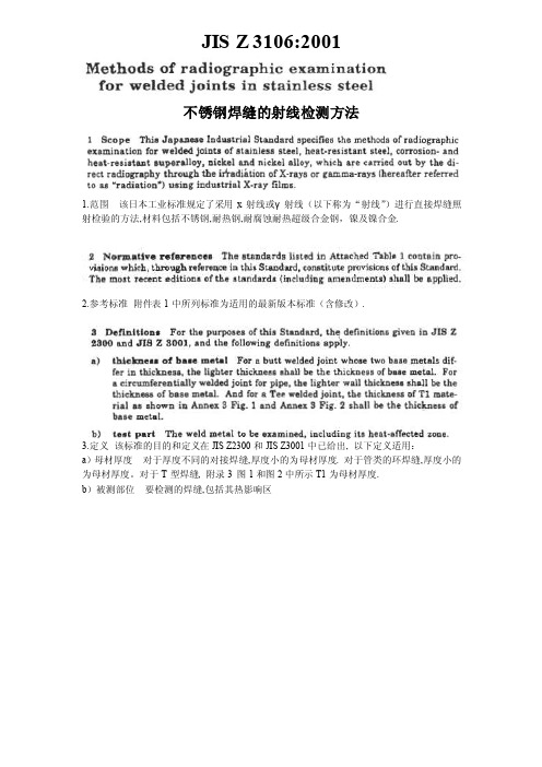
Circular 97 Series Threaded Connectors
with Solder Contacts (MIL-C-5015 Type)
Underwriters Laboratories approved recognition File E115497. Canadian Standard Association Certification File LR69183
—
3/4
7/8
—
5/8-24
—
10.40 7.28 5.41 1-7/16
—
25/32
1
—
5/8-24
—
11.13 7.79 5.79
10.43 7.30 5.43
12.30 8.61 6.40
10.38 7.27 5.40 1-15/32 —
7/8 1-1/8 —
3/4-20
—
12.88 9.02 6.70
D
FE
22-19 A
D
A
C
B
22-22
A
L
B
K
M
C
PN
J
O
D
I
E
H GF
24-7 A
A BC
D
E
MS3106B12S-8S中文资料
Dimensions are shown in mm (inch) Dimensions subject to change
2
元器件交易网
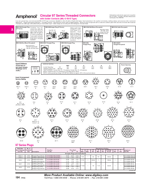
Circular
Contact Cavity Arrangements
CA/MS A&B
10SL-3
CA/MS A&B
Contact Arrangement 10SL-3 10SL-4 12S-3 14S-1 14S-2 14S-5 14S-6 14S-7
W˚ — — 70 — — — — 90
X˚ — — 145 — 120 110 — 180
Y˚ — — 215 — 240 — — 270
Z˚ — — 290 — — — — —
Dimensions are shown in mm (inch) Dimensions subject to change
1
元器件交易网
Circular
How to Order
CA/MS A&B
SERIES PREFIX MS – Complies with Military Specification MIL-C-5015 CA – Cannon prefix indicating special application or variation of MS SHELL STYLE 3100 – Wall Mounting Receptacle (A version only) 3101 – Cord Connector Plug (A version only) 3102 – Box Mounting Receptacle 3106 – Straight Plug 3108 – 90° Angle Plug (B version only)
MS3106K16S中文资料
FINISHES
Shell - Olive drab over cadmium plate Contacts - Silver plate
MECHANICAL FEATURES
Shell Size - In sixteenths of an inch Coupling - Threaded Contact Arrangements - See pages 216-217
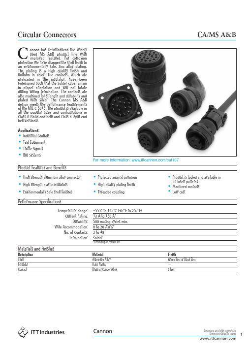
MS-K
tacts; thermocouple contacts must be orderd separately and are solder type unless otherwise requested on order. Cavities that will contain the thermocouple contacts and contact material must be specified when ordering.
• Receptacles in size 10SL are available with pin inserts only. Part Number MS3100K8S-*†
* Add contact arrangment. See pages 216-217. A Thread 1/2-28UNEF-2A 5/8-24UNEF-2A 3/4-20UNEF-2A 7/8-20UNEF-2A 1-20UNEF-2A 1-20UNEF-2A 1-1/8-18UNEF-2A 1-1/4-18UNEF-2A 1-3/8-18UNEF-2A 1-1/2-18UNEF-2A 1-3/4-18UNS-2A 2-18UNS-2A 2-1/4-16UN-2A
Sபைடு நூலகம்(TYP.)
思博特 条码打印机G-3106

G系列用户手册声明此为A级产品,在生活环境中,该产品可能会造成无线电干扰。
在这种情况下,可能需要用户对其干扰采取切实可行的措施。
商标ARM是Advanced RISC Machines Ltd.的注册商标。
Centronics是Centronics Data Computer Corporation的注册商标。
Microsoft, Windows是Microsoft Corporation的注册商标。
POSTEK是深圳市博思得科技发展有限公司的注册商标。
PS/2是International Business Machines Corporation的注册商标。
版权版权所有2004-2011深圳市博思得科技发展有限公司保留一切版权。
G系列标签打印机用户手册。
二○一一年二月第十版。
免除责任声明本手册在其出版时,确切地阐述了POSTEK G系列G-2108、G-3106、G-2108D、G-3106D四个型号标签打印机的规格和使用说明。
但是其后生产的打印机的规格以及配置可能会在没有任何通告的情况下改变。
该产品的制造商和经销商对于由本手册和打印机之间存在的差异甚至错误所造成的直接或间接的损失不承担任何责任。
尽管本手册对可能发生的问题进行了尽可能详尽的描述,但是不保证实际使用该打印机的过程中仍有未预见的情况发生。
对于使用该打印机中发生的诸如打印机不工作、打印的内容缺损或不清晰等问题,该产品的制造商和经销商只负责排除该打印机的故障(依照保修卡上的保修条款),而对于其它任何直接或间接的损失包括商业利益损失、业务中断损失、商业信息丢失或其它财务损失等不承担责任。
iG系列用户手册重要安全事项在没有该产品制造商授权人员指导下,严禁私自拆装这台打印机及其电源适配器,否则可能会发生触电、打印机的传动机构伤人或损坏机器零部件的事故。
严禁使用损坏的或破旧的电源线,否则可能会造成触电或引发火灾。
严禁过度弯曲、用力拉扯电源线。
6639S-1-103;6639S-1-102;6639S-1-104;6639S-1-202;6639S-1-203;中文规格书,Datasheet资料
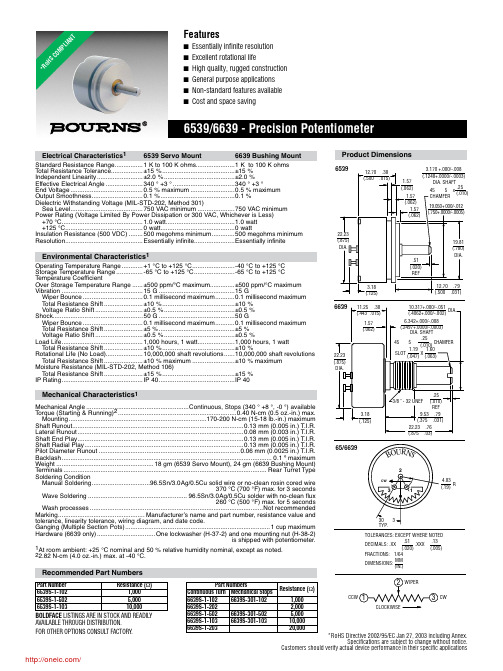
22.23 (.875) DIA.
3.18 (.125)
6639
11.25 .38 (.443 .015)
1.57 (.062)
Байду номын сангаас
22.23 (.875) DIA.
.51 (.020) REF
19.81 (.780) DIA.
12.70 .79 (.500 .031)
10.317+.000/-.051 (.4062+.000/-.002)
DIA.
6.342+.000/-.008
(.2497+.0000/-.0003) DIA. SHAFT .25
45 5 (.010) CHAMFER 1.19 1.60
SLOT (.047) X (.063)
Mechanical Characteristics1
Mechanical Angle ..........................................................Continuous, Stops (340 ° +8 °, -0 °) available Torque (Starting & Running)2 ...................................................................0.40 N-cm (0.5 oz.-in.) max.
Sea Level......................................... 750 VAC minimum .....................750 VAC minimum Power Rating (Voltage Limited By Power Dissipation or 300 VAC, Whichever is Less)
MS3102E-16S-1P中文资料

Straight Plug w/Socket
97-3106A-10SL-3S-ND 97-3106A-10SL-4S-ND
97-3106A-12S-3P-ND 97-3106A-12S-3S-ND
97-3106A-14S-1P-ND 97-3106A-14S-1S-ND 97-3106A-14S-2P-ND 97-3106A-14S-2S-ND
20-16
9/2#12, Straight Plug w/Pins 9/7#16 Straight Plug w/Socket
20-27
14/16 Straight Plug w/Pins Straight Plug w/Socket
20-29
17/16 Straight Plug w/Pins Straight Plug w/Socket
Y
Amphenol
Ref. Part No.
97-3106A-10SL-3S
—
97-3106A-10SL-4S
—
97-3106A-12S-3P
97-3106A-12S-3S
97-3106A-14S-1P
97-3106A-14S-1S
—
97-3106A-14S-2P
97-3106A-14S-2S
(Continued)
DC
250
700
1250
1750
Voltages at Sea Level AC(rms)
200
500
900
1250
TEST CURRENT: Contact Size 16 = 13 amperes, Contact Size 12 = 23 amperes