FQP5N50C中文资料
FQP13N50C中文资料
--
--
IGSSF IGSSR
Gate-Body Leakage Current, Forward VGS = 30 V, VDS = 0 V Gate-Body Leakage Current, Reverse VGS = -30 V, VDS = 0 V
--
--
--
--
--
--
1 10 100 -100
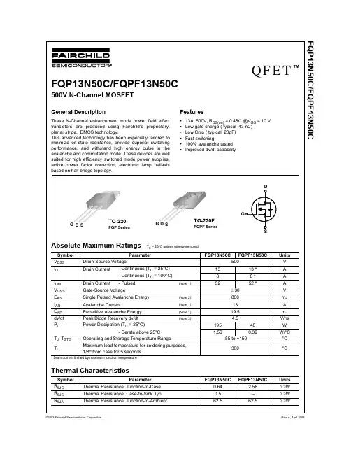
FQP13N50C FQPF13N50C
500
13
13 *
8
8*
52
52 *
± 30
860
13
19.5
4.5
195
48
1.56
0.39
-55 to +150
300
Units V A A A V mJ A mJ
V/ns W
W/°C °C
°C
Thermal Characteristics
Symbol RθJC RθJS RθJA
2.0 --
4.0
V
VGS = 10 V, ID = 6.5 A
-- 0.39 0.48
Ω
VDS = 40 V, ID = 6.5 A
(Note 4) --
15
--
S
Dynamic Characteristics
Ciss
Input Capacitance
Coss
Output Capacitance
Crss
Drain Current - Continuous (TC = 25°C)
- Continuous (TC = 100°C)
IDM
Drain Current - Pulsed
MAX5075C中文资料
General DescriptionThe MAX5075 is a +4.5V to +15V push-pull, current-fed topology driver subsystem with an integrated oscillator for use in telecom module power supplies. The device drives two MOSFETs connected to a center-tapped transformer primary providing secondary-side, isolated,negative or positive voltages. This device features a pro-grammable, accurate, integrated oscillator with a syn-chronizing clock output that synchronizes an external PWM regulator. A single external resistor programs the internal oscillator frequency from 50kHz to 1.5MHz.The MAX5075 incorporates a dual MOSFET driver with ±3A peak drive currents and 50% duty cycle. The MOSFET driver generates complementary signals to drive external ground-referenced n-channel MOSFETs.The MAX5075 is available with a clock output frequency to MOSFET driver frequency ratio of 1x, 2x, and 4x. The MAX5075 is available in a thermally enhanced 8-pin µMAX ®package and is specified over the -40°C to +125°C operating temperature range.ApplicationsCurrent-Fed, High-Efficiency Power-Supply Modules Power-Supply Building Subsystems Push-Pull Driver SubsystemsFeatures♦Current-Fed, Push-Pull Driver Subsystem ♦Programmable, Accurate Internal Oscillator ♦Single +4.5V to +15V Supply Voltage Range ♦Dual ±3A Gate-Drive Outputs♦1mA Operating Current at 250kHz with No Capacitive Load ♦Synchronizing Clock Frequency Generation Options ♦Thermally Enhanced 8-Pin µMAX Package ♦-40°C to +125°C Operating Temperature RangeMAX5075Push-Pull FET Driver with Integrated Oscillatorand Clock Output________________________________________________________________Maxim Integrated Products 1Ordering Information19-3662; Rev 0; 5/05For pricing, delivery, and ordering information,please contact Maxim/Dallas Direct!at 1-888-629-4642, or visit Maxim’s website at .Pin Configuration appears at end of data sheet.*EP = Exposed paddle.Note:All devices specified for -40°C to +125°C operating temperature range.µMAX is a registered trademark of Maxim Integrated Products, Inc.M A X 5075and Clock Output 2_______________________________________________________________________________________ABSOLUTE MAXIMUM RATINGSELECTRICAL CHARACTERISTICS(V CC = +12V, R RT = 124k Ω, NDRV1 = NDRV2 = open, T A = T J = -40°C to +125°C, unless otherwise noted. Typical values are measuredStresses beyond those listed under “Absolute Maximum Ratings” may cause permanent damage to the device. These are stress ratings only, and functional operation of the device at these or any other conditions beyond those indicated in the operational sections of the specifications is not implied. Exposure to absolute maximum rating conditions for extended periods may affect device reliability.V CC to DGND, PGND.............................................-0.3V to +18V CLK, RT to DGND.....................................................-0.3V to +6V NDRV1, NDRV2 to PGND...........................-0.3V to (V CC + 0.3V)DGND to PGND.....................................................-0.3V to +0.3V CLK Current......................................................................±20mA NDRV1, NDRV2 Peak Current (200ns)..................................±5A NDRV1, NDRV2 Reverse Current (Latchup Current)......±500mAContinuous Power Dissipation (T A = +70°C)8-Pin µMAX (derate 10.3mW/°C above +70°C)...........825mW Operating Temperature Range .........................-40°C to +125°C Maximum Junction Temperature.....................................+150°C Storage Temperature Range.............................-60°C to +150°C Lead Temperature (soldering, 10s).................................+300°CNote 2:Use the following formula to calculate the MAX5075 oscillator frequency: f OSC = 1012/(32 x R RT ).Note 3:The accuracy of the oscillator’s frequency is lower at frequencies greater than 1MHz.MAX5075and Clock Output_______________________________________________________________________________________3Typical Operating Characteristics(V CC = +12V, R RT = 124k Ω, NDRV_ = open, CLK = open.)SUPPLY CURRENT vs. SUPPLY VOLTAGESUPPLY VOLTAGE (V)S U P P L Y C U R R E N T (m A )14131211109876512345670415SUPPLY CURRENTvs. C CLKC CLK (pF)S U P P L Y C U R R E N T (m A)806040201.051.101.151.201.251.301.351.401.451.501.000100TEMPERATURE (°C)100752550-25-50125SUPPLY CURRENT vs. TEMPERATURES U P P L Y C U R RE N T (m A )1.021.041.061.081.101.121.141.161.181.201.00CLK RISE TIME vs. SUPPLY VOLTAGESUPPLY VOLTAGE (V)C L K R I S E T I M E (n s )14131112678910551015202530354045500415CLK RISE TIME vs. TEMPERATURETEMPERATURE (°C)C L K R I S E T I M E(n s )1007550250-2537.037.538.038.539.039.536.5-501252468101214CLK FALL TIME vs. SUPPLY VOLTAGESUPPLY VOLTAGE (V)C L K F A L L T I M E (n s )141311126789105415CLK FALL TIME vs. TEMPERATURETEMPERATURE (°C)C L K F A L L T I M E (n s )100755025-25246810120-50125O S C I L L A T O R F R E Q U E N C Y (k H z )244246248250252254256242OSCILLATOR FREQUENCY vs. SUPPLY VOLTAGESUPPLY VOLTAGE (V)141311126789105415M A X 5075and Clock Output 4_______________________________________________________________________________________Typical Operating Characteristics (continued)(V CC = +12V, R RT = 124k Ω, NDRV_ = open, CLK = open.)OSCILLATOR FREQUENCY vs. R RTR RT (k Ω)O S C I L L A T O R F R E Q U E N C Y (k H z )100100100010,00010101000NDRV FREQUENCY vs. CLK FREQUENCYCLK FREQUENCY (kHz)N D R V F R E Q U E N C Y (k H z )12501000250500750100200300400500600700800001500MAX5075A WAVEFORM2µs/divNDRV15V/divNDRV25V/divCLK 5V/divR RT = 124k ΩMAX5075B WAVEFORMMAX5075 toc122µs/divNDRV15V/divNDRV25V/div CLK 5V/divR RT = 124k ΩMAX5075C WAVEFORMMAX5075 toc134µs/divNDRV15V/divNDRV25V/divCLK 5V/divR RT = 124k ΩMAX5075and Clock Output_______________________________________________________________________________________5Figure 1. MAX5075 Functional DiagramM A X 5075Detailed DescriptionThe MAX5075 is a +4.5V to +15V push-pull, current-fed topology driver subsystem with an integrated oscillator for use in 48V module power supplies.The MAX5075 features a programmable, accurate inte-grated oscillator with a synchronizing clock output that can be used to synchronize an external PWM stage. A single external resistor programs the internal oscillator frequency from 50kHz to 1.5MHz.The MAX5075 incorporates a dual MOSFET driver with ±3A peak drive currents and a 50% duty cycle. The MOSFET driver generates complementary signals to drive external ground-referenced n-channel MOSFETs.The MAX5075 is available with a clock output frequency to MOSFET driver frequency ratios of 1x , 2x, and 4x.Internal OscillatorAn external resistor at RT programs the MAX5075internal oscillator frequency from 50kHz to 1.5MHz. The MAX5075A/B NDRV1 and NDRV2 switching frequen-cies are one-half the programmed oscillator frequency with a nominal 50% duty cycle. The MAX5075C NDRV1and NDRV2 switching frequencies are one-fourth the oscillator frequency.Use the following formula to calculate the internal oscil-lator frequency:where f OSC is the oscillator frequency and R RT is a resistor connected from RT to DGND in ohms.Place a 1nF capacitor from RT to DGND for stability and to filter out noise.Synchronizing Clock OutputThe MAX5075 provides a buffered clock output that can be used to synchronize the oscillator input of a PWM con-troller. CLK is powered from an internal 5V regulator and sources/sinks up to 10mA. The MAX5075 has internal CLK output frequency to NDRV1 and NDRV2 switching frequency ratios set to 1x, 2x, or 4x (Table 1).The MAX5075A has a CLK frequency to NDRV_ frequen-cy ratio set to 1x. The MAX5075B has a CLK frequency to NDRV_ frequency ratio set to 2x and the MAX5075C has a CLK frequency to NDRV_ frequency ratio set to 4x.There is a typical 30ns delay from CLK to NDRV_ output.Applications InformationSupply BypassingPay careful attention to bypassing and grounding the MAX5075. Peak supply and output currents may exceed 3A when driving large MOSFETs. Ground shifts due to insufficient device grounding may also disturb other cir-cuits sharing the same ground-return path. Any series inductance in the V CC , NDRV1, NDRV2, and/or GND paths can cause noise due to the very high di/dt when switching the MAX5075 with any capacitive load. Place one or more 0.1µF ceramic capacitors in parallel as close to the device as possible to bypass V CC to PGND. Use a ground plane to minimize ground-return resistance and inductance. Place the external MOSFETs as close as possible to the MAX5075 to further minimize board induc-tance and AC path impedance.and Clock Output 6_______________________________________________________________________________________Table 1. MAX5075 CLK Output FrequencyPower Dissipation The power dissipation of the MAX5075 is a function of the sum of the quiescent current and the output current (either capacitive or resistive load). Maintain the sum of the currents so the maximum power dissipation limit is not exceeded. The power dissipation (P DISS) due to the quiescent switching supply current (I CCSW) can be cal-culated as:P DISS= V CC x I CCSWFor capacitive loads, use the following equation to esti-mate the power dissipation:P LOAD= 2 x C LOAD x V CC2 x f NDRV_where C LOAD is the capacitive load at NDRV1 and NDRV2, V CC is the supply voltage, and f NDRV_is the MAX5075 NDRV_ switching frequency.Calculate the total power dissipation (P T) as follows:P T = P DISS + P LOADLayout Recommendations The MAX5075 sources and sinks large currents that can create very fast rise and fall edges at the gate of the switching MOSFETs. The high di/dt can cause unaccept-able ringing if the trace lengths and impedances are not well controlled. Use the following PC board layout guide-lines when designing with the MAX5075:•Place one or more 0.1µF decoupling ceramic capacitors from V CC to PGND as close to the device as possible. Connect V CC and all ground pins to large copper areas. Place one bulk capaci-tor of 10µF on the PC board with a low-impedance path to the V CC input and PGND of the MAX5075.•Two AC current loops form between the device and the gate of the driven MOSFETs. The MOSFETslook like a large capacitance from gate to sourcewhen the gate pulls low. The current loop is fromthe MOSFET gate to NDRV1 and NDRV2 of theMAX5075, to PGND, and to the source of theMOSFET. When the gate of the MOSFET pulls high,the current is from the V CC terminal of the decou-pling capacitor, to V CC of the MAX5075, to NDRV1and NDRV2, and to the MOSFET gate and source.Both charging current and discharging current loopsare important. Minimize the physical distance andthe impedance in these AC current paths.•Keep the device as close to the MOSFET as possible.Chip Information TRANSISTOR COUNT: 1335PROCESS: BiCMOSMAX5075 and Clock Output_______________________________________________________________________________________7M A X 5075and Clock Output Maxim cannot assume responsibility for use of any circuitry other than circuitry entirely embodied in a Maxim product. No circuit patent licenses are implied. Maxim reserves the right to change the circuitry and specifications without notice at any time.8_____________________Maxim Integrated Products, 120 San Gabriel Drive, Sunnyvale, CA 94086 408-737-7600©2005 Maxim Integrated ProductsPrinted USAis a registered trademark of Maxim Integrated Products, Inc.Package Information(The package drawing(s) in this data sheet may not reflect the most current specifications. For the latest package outline information go to /packages .)。
FQPF13N50中文资料

Notes:1. Repetitive Rating : Pulse width limited by maximum junction temperature2. L = 9.3mH, I AS = 12.5A, V DD = 50V, R G = 25 Ω, Starting T J = 25°C3. I SD ≤ 13.4A, di/dt ≤ 200A/µs, V DD ≤ BV DSS, Starting T J = 25°C4. Pulse Test : Pulse width ≤300µs, Duty cycle ≤2%5. Essentially independent of operating temperatureOn CharacteristicsV GS(th)Gate Threshold Voltage V DS = V GS , I D = 250 µA3.0-- 5.0V R DS(on)Static Drain-Source On-ResistanceV GS = 10 V, I D = 6.25 A--0.330.43Ωg FSForward TransconductanceV DS = 50 V, I D = 6.25 A--10--SDynamic CharacteristicsC iss Input Capacitance V DS = 25 V, V GS = 0 V,f = 1.0 MHz--18002300pF C oss Output Capacitance--245320pF C rssReverse Transfer Capacitance--2535pFSwitching Characteristicst d(on)Turn-On Delay Time V DD = 250 V, I D = 13.4 A,R G = 25 Ω--4090ns t r Turn-On Rise Time --140290ns t d(off)Turn-Off Delay Time --100210ns t f Turn-Off Fall Time --85180ns Q g Total Gate Charge V DS = 400 V, I D = 13.4 A,V GS = 10 V--4560nC Q gs Gate-Source Charge --11--nC Q gdGate-Drain Charge--22--nCDrain-Source Diode Characteristics and Maximum RatingsI S Maximum Continuous Drain-Source Diode Forward Current ----12.5A I SM Maximum Pulsed Drain-Source Diode Forward Current----50A V SD Drain-Source Diode Forward Voltage V GS = 0 V, I S = 12.5 A ---- 1.4V t rr Reverse Recovery Time V GS = 0 V, I S = 13.4 A,dI F / dt = 100 A/µs--290--ns Q rrReverse Recovery Charge--2.6--µC(Note 4) (Note 4, 5)(Note 4, 5)(Note 4)DISCLAIMERFAIRCHILD SEMICONDUCTOR RESERVES THE RIGHT TO MAKE CHANGES WITHOUT FURTHER NOTICE TO ANY PRODUCTS HEREIN TO IMPROVE RELIABILITY , FUNCTION OR DESIGN. FAIRCHILD DOES NOT ASSUME ANY LIABILITY ARISING OUT OF THE APPLICATION OR USE OF ANY PRODUCT OR CIRCUIT DESCRIBED HEREIN; NEITHER DOES IT CONVEY ANY LICENSE UNDER ITS PATENT RIGHTS, NOR THE RIGHTS OF OTHERS.TRADEMARKSThe following are registered and unregistered trademarks Fairchild Semiconductor owns or is authorized to use and is not intended to be an exhaustive list of all such trademarks.LIFE SUPPORT POLICYFAIRCHILD S PRODUCTS ARE NOT AUTHORIZED FOR USE AS CRITICAL COMPONENTS IN LIFE SUPPORTDEVICES OR SYSTEMS WITHOUT THE EXPRESS WRITTEN APPROVAL OF FAIRCHILD SEMICONDUCTOR CORPORATION.As used herein:1. Life support devices or systems are devices orsystems which, (a) are intended for surgical implant intothe body, or (b) support or sustain life, or (c) whosefailure to perform when properly used in accordancewith instructions for use provided in the labeling, can be reasonably expected to result in significant injury to the user.2. A critical component is any component of a life support device or system whose failure to perform can be reasonably expected to cause the failure of the life support device or system, or to affect its safety or effectiveness.PRODUCT STATUS DEFINITIONS Definition of Terms Datasheet Identification Product Status DefinitionAdvance InformationPreliminaryNo Identification Needed Obsolete This datasheet contains the design specifications for product development. Specifications may change in any manner without notice.This datasheet contains preliminary data, andsupplementary data will be published at a later date.Fairchild Semiconductor reserves the right to make changes at any time without notice in order to improve design.This datasheet contains final specifications. Fairchild Semiconductor reserves the right to make changes at any time without notice in order to improve design.This datasheet contains specifications on a product that has been discontinued by Fairchild semiconductor.The datasheet is printed for reference information only.Formative or In Design First ProductionFull ProductionNot In ProductionImpliedDisconnect ISOPLANARLittleFETMicroFETMicroPakMICROWIREMSXMSXProOCXOCXProOPTOLOGIC âOPTOPLANARFACT FACT Quiet Series FAST âFASTr FRFET GlobalOptoisolator GTO HiSeCI 2CRev. I2ACEx ActiveArray Bottomless CoolFET CROSSVOLT DOME EcoSPARK E 2CMOS TM EnSigna TMPACMANPOP Power247 PowerTrench âQFET QS QT Optoelectronics Quiet Series RapidConfigure RapidConnect SILENT SWITCHER âSMART START SPMStealthSuperSOT -3SuperSOT -6SuperSOT -8SyncFET TinyLogic âTruTranslation UHC UltraFET âVCXAcross the board. Around the world. The Power FranchiseProgrammable Active Droop。
550C中文资料
550C中文资料在科技发展日新月异的现代社会中,人们越来越离不开各种电子设备。
而对于电子设备的选购和使用,掌握相关的中文资料是非常重要的。
本文将为大家介绍一款名为550C的电子设备,并提供相关的中文资料,以帮助读者更好地了解和使用它。
一、550C的基本介绍550C是一款功能强大的电子设备,集合了手机、平板电脑和笔记本电脑的诸多优点于一身。
它拥有高性能的处理器、大容量的存储空间和精美的显示屏,是一款非常实用的移动办公工具。
同时,550C还具备多种连接方式,包括蓝牙、Wi-Fi和USB等,方便用户与其他设备进行数据传输和共享。
此外,550C还内置了多种实用应用程序,如浏览器、日历、邮件等,满足用户的多种需求。
二、550C的主要特点1. 高性能处理器:550C搭载了最新一代的处理器,运行速度快,能够处理各类任务和应用程序。
2. 大容量存储空间:550C拥有大容量的存储空间,用户可以存储大量的文件、照片和视频等。
3. 精美显示屏:550C采用了高分辨率的显示屏,画质清晰细腻,色彩鲜明逼真,让用户享受更佳的视觉体验。
4. 多种连接方式:550C支持蓝牙、Wi-Fi和USB等多种连接方式,用户可以便捷地与其他设备进行数据传输和共享。
5. 多功能应用程序:550C内置了浏览器、日历、邮件等多种实用应用程序,方便用户进行各类操作和管理。
三、使用550C的注意事项1. 保护屏幕:550C的显示屏非常精美,用户在使用过程中应尽量避免划伤或碰撞屏幕,以延长其使用寿命。
2. 定期清理内存:550C的存储空间虽然大,但也需要定期清理,以免影响设备的运行速度和性能。
3. 注意个人信息安全:在使用550C进行网络浏览和支付等操作时,务必注意个人信息的安全,避免泄露。
4. 防止过度充电:当550C电池电量已满时,应尽量避免继续给其充电,以免损害电池寿命。
四、550C的维护和保养1. 定期升级系统:550C的系统会不定期推出新的升级版本,用户应定期进行系统升级,以享受更完善的功能和更好的使用体验。
RFP50N05资料
RFG50N05, RFP50N05 50 50 50 120 ±20 132 0.88
Refer to UIS SOA Curve -55 to 175
300 260
UNITS V V A A V W
W/ oC
oC
oC oC
CAUTION: Stresses above those listed in “Absolute Maximum Ratings” may cause permanent damage to the device. This is a stress only rating and operation of the device at these or any other conditions above those indicated in the operational sections of this specification is not implied.
IDSS
IGSS rDS(ON)
t(ON) td(ON)
tr
VDS = Rated BVDSS, VGS = 0V VDS = 0.8 x Rated BVDSS, VGS = 0V, TJ = 150oC
VGS = ±20V
ID = 50A, VGS = 10V (Figure 7)
VDD = 25V, ID ≈ 25A, RL = 1.0Ω, RGS = 6.67Ω, VGS = 10V (Figure 11)
or 407-727-9207 | Copyright © Intersil Corporation 1999
元器件交易网
RFG50N05, RFP50N05
Absolute Maximum Ratings TC = 25oC, Unless Otherwise Specified
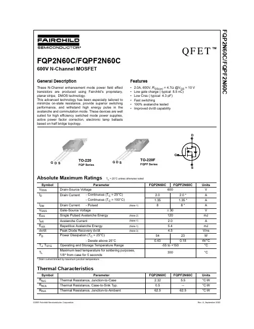
FQPF2N60C资料
100
150℃ 25℃
※ Notes :
1. 2.
2V5GS0μ=s0VPulse
Test
10-1
0.2
0.4
0.6
0.8
1.0
1.2
1.4
VSD, Source-Drain voltage [V]
Figure 4. Body Diode Forward Voltage Variation with Source Current and Temperature
VGS = 0 V, IS = 2 A,
-- 230
--
ns
Qrr
Reverse Recovery Charge
dIF / dt = 100 A/µs
(Note 4) --
1.0
--
µC
Notes:
1. Repetitive Rating : Pulse width limited by maximum junction temperature
Parameter Thermal Resistance, Junction-to-Case Thermal Resistance, Case-to-Sink Typ. Thermal Resistance, Junction-to-Ambient
FQP2N60C 2.32 0.5 62.5
FQPF2N60C 5.5 -62.5
元器件交易网
FQP2N60C/FQPF2N60C
FQP2N60C/FQPF2N60C
600V N-Channel MOSFET
QFET TM
General Description
These N-Channel enhancement mode power field effect transistors are produced using Fairchild’s proprietary, planar stripe, DMOS technology. This advanced technology has been especially tailored to minimize on-state resistance, provide superior switching performance, and withstand high energy pulse in the avalanche and commutation mode. These devices are well suited for high efficiency switched mode power supplies, active power factor correction, electronic lamp ballasts based on half bridge topology.
C2590中文资料
Designed to meet today's requirements for 2.5V applications. The C25xx Series utilizes only fundamental and 3rd overtone crystal designs. No multiplier is used thereby reducing output jitter. Available on 16mm tape and reel in quantities of 1K.
260°C 217°C 200°C 150°C
Ramp-Up 3°C/Sec Max. Critical Temperature Zone Ramp-Down 6°C/Sec.
Crystek Part Number Guide
Example: C2592-44.736MHZ Example: CE2592-44.736MHZ Temperature
TD-02062 Rev.E
pin 3 OSC.
GND
PWR Supply
O/P Load incl Probe Cl
VM
Bypass Cap. pin 1
pin 2
High Impedance GND or "LOW"
Oscillation OPEN or "HIGH"
Specifications subject to change without notice.
-10/ 70°C -40/ 85°C
Frequency Stability +/- 100ppm +/- 50ppm +/- 25ppm +/- 20ppm
ICP-N50中文资料
Overcurrent Protection Elements Rev.A 1/5Circuit protection elementsz Circuit protection elementsRohm’s circuit protectors have a very reliable current cut-off capability that protects ICs and their circuits from accidental short circuit loads. Whether operated in AC or DC circuits, these circuit protectors have a very low internal resistance in normal operation, but safely and rapidly break the circuit when the current cutoff level is exceeded.z Features1) Cutoff is sharp and repeatable.2) Low internal resistance and minimal voltage drop. 3) Incombustible. 4) Compact.5) Rated for continuous use.6) Good temperature characteristics. 7) Withstands surges well.8) UL certified (UL certification number E107856).z ApplicationCurrent surge protectionz Operation notesDo not use this product on the primary side of commercial power supplies. Arcs that result after cutoff may damage the molding.Surface mounting Typez ICP-S seriesICP-S0.5ICP-S0.7ICP-S1.0ICP-S1.20.50.71.01.20.1500.0840.06150−55 to +125−55 to +1250.048Fig.1Fig.2Fig.3Fig.4Product name Rated current (A)Internal resistance Typ.(Ω)Cutoff characteristics Rated voltage (V)Operating temperature (°C)Storage temperature (°C)Overcurrent Protection Elements Rev.A 2/5z Cutoff characteristicsFig.1 ICP-S0.5C U T O F F T I M E : (S )CUTOFF CURRENT : (A)Fig.2 ICP-S0.7C U T O F F T I M E : (S )CUTOFF CURRENT : (A)Fig.3 ICP-S1.0C U T O F F T I M E : (S )CUTOFF CURRENT : (A)Fig.4 ICP-S1.2C U T O F F T I M E : (S )CUTOFF CURRENT : (A)The cutoff characteristics shown are typical. For further details of how to use these protectors, please request the technical documentation from your Rohm representative.z External dimensions (Unit : mm)Overcurrent Protection Elements Rev.A 3/5z Packaging specificationsPackage typeTaping Symbol TN ICP-S2000Type ICP-S0.5ICP-S0.7ICP-S1.0ICP-S1.2Basic ordering unit (pieces)z Taping specifications (Unit : mm)Overcurrent Protection Elements Rev.A 4/5Leaded typeICP-N seriesICP-N10ICP-N15ICP-N20ICP-N25ICP-N38ICP-N500.40.60.81.01.52.00.2200.1350.10050−55 to +125−55 to +1250.0700.0420.035Fig.1Fig.2Fig.3Fig.4Fig.5Fig.6ICP-N702.50.023Fig.7Product nameRated current (A)Internal resistance Typ.(Ω)Cutoff characteristics Rated voltage (V)Operating temperature (°C)Storage temperature(°C)z Cutoff characteristicsFig.1 ICP-N10C U T O F F T I M E : (S )CUTOFF CURRENT : (A)Fig.2 ICP-N15C U T O F F T I M E : (S )CUTOFF CURRENT : (A)Fig.3 ICP-N20C U T O F F T I M E : (S )CUTOFF CURRENT : (A)Fig.4 ICP-N25C U T O F F T I M E : (S )CUTOFF CURRENT : (A)Fig.5 ICP-N38C U T O F F T I M E : (S )CUTOFF CURRENT : (A)Fig.6 ICP-N50C U T O F F T I M E : (S )CUTOFF CURRENT : (A)Overcurrent Protection Elements Rev.A 5/5Fig.7 ICP-N70C U T O F F T I M E : (S )CUTOFF CURRENT : (A)The cutoff characteristics given represent typical values. T echnical documentation regarding ways of using circuit protectors is available from your Rohm representative.z External dimensions (Unit : mm)z Packaging specificationsPackaging type Taping Symbol T104ICP-N3000TypeICP-N10/N15/N20/N25/N38/N50/N70Basic orderingunit (pieces)z Taping specifications (Unit : mm)AppendixAbout Export Control Order in JapanProducts described herein are the objects of controlled goods in Annex 1 (Item 16) of Export T rade ControlOrder in Japan.In case of export from Japan, please confirm if it applies to "objective" criteria or an "informed" (by MITI clause)on the basis of "catch all controls for Non-Proliferation of Weapons of Mass Destruction.Appendix1-Rev1.1。
C1250资料
Vectron International· v.2005-08-05-05 · page 1 of 4 SEMVectron International Frequency Range1 to 800 MHz (ACMOS and TTL outputs available up to 125 MHz. LVPECL and LVDS output frequencies above 220 MHz are achieved through the use of a PLL multiplier.)Standard Frequencies 19.44, 32.768, 44.736, 51.84, 77.76, 155.52, 622.08 MHzFrequency Stabilities 1ParameterMin TypMax Units Condition Ordering Code5Operating temperature range -100 +100 ppm 0 +70°C C104 (referenced to +25°C)-50 +50 ppm 0 +70°C C505 -25 +25 ppm 0 +70°C C255 -15 +15 ppm 0 +70°C C155 -100 +100 ppm -40 +85°C F104 -50 +50 ppm -40 +85°C F505 -25 +25 ppm -40 +85°C F255 -100 +100 ppm -55 +125°C M104 -65 +65 ppm -55 +125°C M655 Initial accuracy (do not use with -15 +15 ppm @ 25°C T155 overall tolerance code below)-25 +25 ppm @ 25°C T255 -50 +50 ppm @ 25°C T505 -100 +100 ppm @ 25°C T104ParameterMin TypMax Units Condition Ordering Code5Overall tolerance (includes operating -100 +100 ppm 0 +70°C TC104 temperature and initial accuracy)7-50 +50 ppm 0 +70°C TC505-25 +25 ppm 0 +70°C TC255 -100 +100 ppm -40 +85°C TF104 -50 +50 ppm -40 +85°C TF505 -100 +100 ppm -55 +125°C TM104 -80+80 ppm -55 +125°C TM805Additional stability parameters: vs. Supply voltage change vs. Load change vs. Aging / 1st yearvs. Aging / year (following years)-2 -1 -3 -1+2 +1 +3 +1ppm ppm ppm ppmV S ± 5% Load ± 5%Supply Voltage (Vs)ParameterMin Typ Max Units ConditionOrdering Code5Supply voltage4.755.05.25 VDC SV050Current consumption 15 mA ACMOS or TTL 1.0 to 23.9 MHZ (+5 VDC)20 mA ACMOS or TTL 24 to 49.9 MHz 40 mA ACMOS or TTL 50 to 125.00 MHzSupply voltage 3.135 3.3 3.465 VDC SV033 Supply voltage2.375 2.52.625 VDC SV025Current consumption 6 mA ACMOS 1.0 to 14.90 MHZ (+3.3 VDC or +2.5 VDC)8 mA ACMOS 15.0 to 39.9 MHz 12 mA ACMOS 40.0 to 59.9 MHz 16 mA ACMOS 60.0 to 84.9 MHz 40 mA ACMOS 85.0 to 125.0 MHz75 mA LVPECL or LVDS No load <200 MHz 100mALVPECL or LVDS No load >200 MHzTypical ApplicationsFeaturesMilitary Systems5X7 Surface Mount Package Avionics and Instrumentation Reflow Process CompatibleTest Equipment ACMOS, TTL, LVPECL and LVDSMedical EquipmentMIL-PRF-55310 Class B Screening (optional) Military Operating Temperature Range (optional)Vectron International· v.2005-08-05-05 · page 2 of 4 SEMVectron International RF OutputParameterMinTyp MaxUnits ConditionOrdering Code5Signal ACMOSRFALoad1550 pF Signal Level (Vol) 0.5 VDC Vs= 5.0V and 15pF load 0.3 VDC Vs=3.3V and 15pF load 0.25VDC Vs=2.5V and 15pF load Signal Level (Voh)4.5 VDC Vs=5.0V and 15pF load 3.0 VDC Vs=3.3V and 15pF load 2.25VDC Vs=2.5V and 15pF loadRise and fall times for ACMOS (measured 10% to 90%) 10 6 3 ns ns ns 1.0 to 23.9 MHz 24.0 to 79.9 MHz 80.0 to 125.0MHz Duty cycle 45 4055 60% %@ 50% Vs< 15 MHz @ 50% Vs > 15 MHzSignal TTLRFT Load10 Signal Level (Vol) 0.5VDC Vs= 5.0V and 15pF load Signal Level (Voh)4.5VDC Vs= 5.0V and 15pF loadRise and fall times for TTL (measured 0.8V to 2.0V) 5 3 ns ns 1.0 to 23.9 MHz 24 to 125 MHz Duty Cycle45 4055 60% % @ 1.4V < 15 MHz @ 1.4V > 15 MHzSignal LVPECLRFPLoad50 Into Vcc-2V or Thevenin Equivalent Signal Level (Vol) Vs -1.62VDC -40 +85°C operating temp Signal Level (Voh)Vs- 1.025VDC -40 +85°C operating tempRise and fall times (measured @ 20% to 80%)1000 600 ps ps <100 MHz > 100 MHz Duty cycle LVPECL 4555 % @ 50% VddJitter (rms) 10 0.5 ps ps BW = 10Hz to 20 MHz BW = 12 kHz to 20 MHz Period Jitter (pk-pk) 40ps10,000 Samples - Rising edgeSignal LVDSRFLLoad60100 140Between outputsSignal Level (Vol)1.2 VDC Signal Level (Voh)1.4 VDC Differential Voltage (Vod)240 330 460 mVpeakCommon Mode (Offset) Voltage (Vos) 1.1251.2 1.375 V Start-up Time10 mS Rise and fall times 6001000 ps measured @ 20% to 80% of VodDuty cycle 4555 % @ 50% of Vod Jitter (rms) 5 1 ps ps BW = 10Hz to 20 MHz BW = 12 kHz to 20 MHz Period Jitter (pk-pk)40ps 10,000 Samples - Rising edgeAdditional ParametersScreening Vectron Verification9V Screening Class B, MIL-PRF-55310, Rev.D BOutput Enable6Logic "0" input = Outputs disabled (Tri-state)Logic "1" or floating input = Outputs enabled ) Standard (All outputs)Logic "0" or floating input = Outputs enabledLogic "1" input = Outputs disabled (Tri-state )Custom (Contact factory for availability)Weight< 2 gramsProcessing & PackingHandling & processing noteVectron International· v.2005-08-05-05 · page 3 of 4 SEMVectron International Standard EnvironmentalsParameterTest ConditionVibration MIL-STD-202, Method 204, Condition G (30 G, 10Hz-2000Hz) ShockMIL-STD-202, Method 213, Condition I (100 G, 6ms, Sawtooth) AccelerationMIL-STD-883, Method 2001, Condition A (5000 G, Y1 Plane)Temperature Cycling MIL-STD-883, Method 1010, Condition B Thermal Shock MIL-STD-883, Method 107, Condition BSolderabilityMIL-STD-202, Method 208Leak Test (Fine and Gross)MIL-STD-883, Method 1014, Condition A1 and C1Absolute Maximum RatingsParameterMinTypMax Units Condition Supply voltage (Vs) 7.0 V Vs=5.0VDC 7.0 V Vs=3.3VDCOperable temperature range -55 +125 °C Storage temperature range-62+125°CEnclosuresType A ACMOS or TTLType B LVPECL or LVDSPackage Codes:CodesHeight CodesHeight A1 = 4 leads0.074 ± 0.007 B1 = 6 leads0.074 ± 0.007 E1 = Enable/Disable pin 1 (1.88 ± 0.178) E1 = Enable/Disable pin 1 (1.88 ± 0.178)X = N/C pin 1 E2 = Enable/Disable pin 2 X = N/C pin 1 and pin 2 T = Tinned J leads 8T = Tinned J leads 8X = No TinningX = No TinningPin ConnectionsPin Connections1 Enable/Disable or N/C 3 RF Output 1 Enable/Disable or N/C4 RF Output2 Ground (case) 4 Supply Voltage2 N/C5 Complementary Output 3 Ground (Case)6 Supply VoltageVectron International· v.2005-08-05-05 · page 4 of 4 SEMVectron InternationalHow to Order this Product: 10Step 1Use this worksheet to forward the following information to your factory representative (example follows):ModelStabilityCodeInitial AccuracyCode(if required)Supply Voltage Code RF Output Code Screening Code Package Code Enable/DisableCodeTinning CodeC1250 C505 T505SV033RFAVA1E1TStep 2The factory representative will then respond with a Vectron Part Number in the following configuration: Model Package CodeDash Dash NumberC1250[Customer Specified Package Code]-[Factory Generated 4 digit number]Typical P/N C1250A1-0001Notes:1Contact factory for improved stabilities or additional product options. Not all options and codes are available at all frequencies, RF outputs and supply voltages.2Unless otherwise stated all values are valid after warm-up time and refer to typical conditions for supply voltage, frequency control voltage, load, temperature (25°C).3Phase noise degrades with increasing output frequency. 4Subject to technical modification. 5Contact factory for availability. 6Contact factory for other options.7Overall stabilities do not require an initial accuracy code.8Leads tinned IAW Vectron International standard procedure (GR-37409). 9Vectron Verification IAW Vectron International standard process (HK-69314). 10Please be sure to specify nominal frequency.。
fqp5n60c的应用原理
fqp5n60c的应用原理1. 简介fqp5n60c是一款具有广泛应用的N-沟道MOSFET(金属氧化物场效应晶体管),广泛用于电源管理、电机控制和电子开关等领域。
本文将介绍fqp5n60c的基本原理及其应用。
2. fqp5n60c的基本原理fqp5n60c采用N-沟道结构,是一种增强型MOSFET。
它由沟道、栅极、漏极和源极四个主要部分组成。
•沟道:沟道是一个N型掺杂层,用于导电。
电流在这个沟道中流动。
•栅极:栅极是通过输入控制信号来改变沟道电阻的部分。
栅极电压的变化会影响沟道的导电能力。
•漏极和源极:漏极和源极是电流的进出口,电流通过漏极从源极流出。
fqp5n60c的工作原理是通过调节栅极电压来控制沟道的导电能力。
当栅极电压高于一定阈值时,沟道会打开,导通电流。
当栅极电压低于阈值时,沟道关闭,截断电流。
通过控制栅极电压可以实现对电流的控制和开关。
3. fqp5n60c的应用fqp5n60c由于其优异的特性,在各种电子领域中得到了广泛应用。
以下是fqp5n60c的几种常见应用:3.1 电源管理fqp5n60c可以用作电源开关,通过控制其导电能力来实现对电源的开关和调节。
它在电源管理中具有低导通电阻、高输入电容和低开关损耗等特点,适用于交流/直流转换器、开关电源和逆变器等电源管理系统。
3.2 电机控制由于fqp5n60c具有较低的导通电阻和较高的开关速度,可以在电机控制中广泛应用。
它可以用作驱动MOSFET,用于电机启动和调速控制。
fqp5n60c的低导通电阻可以减少能量损耗,提高电机的效率。
3.3 电子开关fqp5n60c作为一个高效可靠的电子开关,可以在电子电路中用于开关操作。
它可以用于开关电源、LED驱动器、电路保护和信号放大器等应用。
其快速开关速度和低开关损耗使其非常适合高频应用。
3.4 其他应用除了上述应用,fqp5n60c还可以在其他电子系统中扮演关键角色。
例如,在电流限制器、电压稳定器和逆变器中,它的优异特性使其成为理想的选择。
- 1、下载文档前请自行甄别文档内容的完整性,平台不提供额外的编辑、内容补充、找答案等附加服务。
- 2、"仅部分预览"的文档,不可在线预览部分如存在完整性等问题,可反馈申请退款(可完整预览的文档不适用该条件!)。
- 3、如文档侵犯您的权益,请联系客服反馈,我们会尽快为您处理(人工客服工作时间:9:00-18:30)。
FQP5N50C/FQPF5N50CNotes:1. Repetitive Rating : Pulse width limited by maximum junction temperature2. L = 21.5 mH, I AS = 5A, V DD = 50V, R G = 25 Ω, Starting T J = 25°C3. I SD ≤ 5A, di/dt ≤ 200A/µs, V DD ≤ BV DSS, Starting T J = 25°C4. Pulse Test : Pulse width ≤ 300µs, Duty cycle ≤ 2%5. Essentially independent of operating temperatureOn CharacteristicsV GS(th)Gate Threshold Voltage V DS = V GS , I D = 250 µA 2.0-- 4.0V R DS(on)Static Drain-Source On-ResistanceV GS = 10 V, I D = 2.5A-- 1.14 1.4Ωg FSForward TransconductanceV DS = 40 V, I D = 2.5A (Note 4)-- 5.2--SDynamic CharacteristicsC iss Input Capacitance V DS = 25 V, V GS = 0 V, f = 1.0 MHz--480625pF C oss Output Capacitance--80105pF C rssReverse Transfer Capacitance--1520pFSwitching Characteristicst d(on)Turn-On Delay Time V DD = 250 V, I D = 5A,R G = 25 Ω(Note 4, 5)--1235ns t r Turn-On Rise Time --46100ns t d(off)Turn-Off Delay Time --50110ns t f Turn-Off Fall Time --48105ns Q g Total Gate Charge V DS = 400 V, I D = 5A,V GS = 10 V(Note 4, 5)--1824nC Q gs Gate-Source Charge -- 2.2--nC Q gdGate-Drain Charge--9.7--nCDrain-Source Diode Characteristics and Maximum RatingsI S Maximum Continuous Drain-Source Diode Forward Current ----5A I SM Maximum Pulsed Drain-Source Diode Forward Current----20A V SD Drain-Source Diode Forward Voltage V GS = 0 V, I S = 5 A ---- 1.4V t rr Reverse Recovery Time V GS = 0 V, I S = 5 A,dI F / dt = 100 A/µs (Note 4)--263--ns Q rrReverse Recovery Charge-- 1.9--µCFQP5N50C/FQPF5N50CDISCLAIMERFAIRCHILD SEMICONDUCTOR RESERVES THE RIGHT TO MAKE CHANGES WITHOUT FURTHER NOTICE TO ANY PRODUCTS HEREIN TO IMPROVE RELIABILITY, FUNCTION OR DESIGN. FAIRCHILD DOES NOT ASSUME ANY LIABILITY ARISING OUT OF THE APPLICATION OR USE OF ANY PRODUCT OR CIRCUIT DESCRIBED HEREIN;NEITHER DOES IT CONVEY ANY LICENSE UNDER ITS PATENT RIGHTS, NOR THE RIGHTS OF OTHERS.LIFE SUPPORT POLICYFAIRCHILD’S PRODUCTS ARE NOT AUTHORIZED FOR USE AS CRITICAL COMPONENTS IN LIFE SUPPORT DEVICES OR SYSTEMS WITHOUT THE EXPRESS WRITTEN APPROVAL OF FAIRCHILD SEMICONDUCTOR CORPORATION.As used herein:1. Life support devices or systems are devices or systems which, (a) are intended for surgical implant into the body,or (b) support or sustain life, or (c) whose failure to perform when properly used in accordance with instructions for use provided in the labeling, can be reasonably expected to result in significant injury to the user.2. A critical component is any component of a life support device or system whose failure to perform can be reasonably expected to cause the failure of the life support device or system, or to affect its safety or effectiveness.PRODUCT STATUS DEFINITIONS Definition of TermsDatasheet Identification Product Status DefinitionAdvance InformationFormative or In Design This datasheet contains the design specifications for product development. Specifications may change in any manner without notice.PreliminaryFirst ProductionThis datasheet contains preliminary data, andsupplementary data will be published at a later date.Fairchild Semiconductor reserves the right to make changes at any time without notice in order to improve design.No Identification Needed Full ProductionThis datasheet contains final specifications. Fairchild Semiconductor reserves the right to make changes at any time without notice in order to improve design.Obsolete Not In ProductionThis datasheet contains specifications on a product that has been discontinued by Fairchild semiconductor.The datasheet is printed for reference information only.TRADEMARKSThe following are registered and unregistered trademarks Fairchild Semiconductor owns or is authorized to use and is not intended to be an exhaustive list of all such trademarks.FACT™FACT Quiet series™FAST ®FASTr™FRFET™GlobalOptoisolator™GTO™HiSeC™I 2C™ImpliedDisconnect™ISOPLANAR™LittleFET™MicroFET™MicroPak™MICROWIRE™MSX™MSXPro™OCX™OCXPro™OPTOLOGIC ®OPTOPLANAR™PACMAN™POP™Power247™PowerTrench ®QFET™QS™QT Optoelectronics™Quiet Series™RapidConfigure™RapidConnect™SILENT SWITCHER ®SMART START™SPM™Stealth™SuperSOT™-3SuperSOT™-6SuperSOT™-8SyncFET™TinyLogic ®TruTranslation™UHC™UltraFET ®VCX™ACEx™ActiveArray™Bottomless™CoolFET™CROSSVOLT ™DOME™EcoSPARK™E 2CMOS™EnSigna™Across the board. Around the world.™The Power Franchise™Programmable Active Droop™。