CY7C1350G-133AXC中文资料
CY7C1352F-133AC中文资料

4.5
ns
205
mA
40
mA
Pin Configuration
100-Pin TQFP
NC
NC
81 A
82 A
85 ADV/LD
86 OE
87 CEN
WE
89 CLK
VSS
VDD
CE3
BWA
BWB
95 NC
96 NC
CE2
CE1
99 A
A
83
84
88
90
91
92
93
94
97
98
100
NC
1
NC
2
NC
• Internally self-timed output buffer control to eliminate the need to use OE
• Byte Write capability • 256K x 18 common I/O architecture • Single 3.3V power supply • 2.5V / 3.3V I/O Operation • Fast clock-to-output times
NC
77
VDDQ
76
VSS
75
NC
74
DQPA
73
DQA
72
DQA
71
VSS
70
VDDQ
69
DQA
68
DQA
67
VSS
BYTE A
66
NC
65
VDD
64
ZZ
63
DQA
62
DQA
61
CY7C1338G-133AXC资料

PRELIMINARY4-Mbit (128K x 32) Flow-Through Sync SRAMCY7C1338GFeatures•128K X 32 common I/O•3.3V –5% and +10% core power supply (V DD)•2.5V or 3.3V I/O supply (V DDQ)•Fast clock-to-output times—6.5 ns (133-MHz version)—7.5 ns (117-MHz version)—8.0 ns (100-MHz version)•Provide high-performance 2-1-1-1 access rate •User-selectable burst counter supporting Intel®Pentium® interleaved or linear burst sequences •Separate processor and controller address strobes •Synchronous self-timed write•Asynchronous output enable•Lead-Free 100-pin TQFP and 119-ball BGA packages •“ZZ” Sleep Mode option Functional Description[1]The CY7C1338G is a 131,072 x 32 synchronous cache RAM designed to interface with high-speed microprocessors with minimum glue logic. Maximum access delay from clock rise is 6.5 ns (133-MHz version). A 2-bit on-chip counter captures the first address in a burst and increments the address automati-cally for the rest of the burst access. All synchronous inputs are gated by registers controlled by a positive-edge-triggered Clock Input (CLK). The synchronous inputs include all addresses, all data inputs, address-pipelining Chip Enable (CE1), depth-expansion Chip Enables (CE2 and CE3), Burst Control inputs (ADSC, ADSP, and ADV), Write Enables(BW[A:D], and BWE), and Global Write (GW). Asynchronous i nputs include the Output Enable (OE) and the ZZ pin.The CY7C1338G allows either interleaved or linear burst sequences, selected by the MODE input pin. A HIGH selects an interleaved burst sequence, while a LOW selects a linear burst sequence. Burst accesses can be initiated with the Processor Address Strobe (ADSP) or the cache Controller Address Strobe (ADSC) inputs. Address advancement is controlled by the Address Advancement (ADV) input. Addresses and chip enables are registered at rising edge of clock when either Address Strobe Processor (ADSP) or Address Strobe Controller (ADSC) are active. Subsequent burst addresses can be internally generated as controlled by the Advance pin (ADV).The CY7C1338G operates from a +3.3V core power supply while all outputs may operate with either a +2.5 or +3.3V supply. All inputs and outputs are JEDEC-standard JESD8-5-compatible.Note:1.For best–practices recommendations, please refer to the Cypress application note System Design Guidelines on .Selection Guide133 MHz 117 MHz 100 MHz Unit Maximum Access Time6.57.58.0ns Maximum Operating Current 225220205mA Maximum Standby Current404040mAShaded areas contain advance information. Please contact your local Cypress sales representative for availability of these parts.Pin Configurations100-Pin TQFPAAAAA 1A 0N C N CV S SV D DN C A AAAA ANC DQ B V DDQ V SSQ DQ B DQ B DQ B DQ B V SSQ V DDQ DQ B DQ B V SS NC V DD DQ A DQ A V DDQ V SSQ DQ A DQ A DQ A DQ A V SSQ V DDQ DQ A DQ A NCNC DQ C DQ C V DDQ V SSQ DQ C DQ CDQ C DQ C V SSQ V DDQ DQ C DQ C NC V DD NC V SS DQ D DQ D V DDQ V SSQ DQ D DQ D DQ D DQ D V SSQ V DDQ DQ D DQ D NCAAC E 1C E 2B W DB W CB W BB W AC E 3V D DV S SC L KG WB W EO E A D S P A A123456789101112131415161718192021222324252627282930313233343536373839404142434445464748495080797877767574737271706968676665646362616059585756555453525110099989796959493929190898887868584838281BYTE ABYTE CAA D V A D S C ZZ M O D E N C BYTE BDQ B BYTE DCY7C1338GPin DefinitionsName I/O DescriptionA0, A1, A Input-Synchronous Address Inputs used to select one of the 128K address location s. Sampled at the rising edge of the CLK if ADSP or ADSC is active LOW, and CE1,CE2, and CE3 are sampled active. A[1:0] feed the 2-bit counter.BW A,BW B BW C,BW DInput-SynchronousByte Write Select Inputs, active LOW. Qualified with BWE to conduct byte writes to the SRAM.Sampled on the rising edge of CLK.GW Input-Synchronous Global Write Enable Input, active LOW. When asserted LOW on the rising edge of CLK, a global write is conducted (ALL bytes are written, regardless of the values on BW[A:D] and BWE).BWE Input-Synchronous Byte Write Enable Input, active LOW. Sampled on the rising edge of CLK. This signal must be asserted LOW to conduct a byte write.CLK Input-Clock Clock Input. Used to capture all synchronous inputs to the device. Also used to increment the burst counter when ADV is asserted LOW, during a burst operation.CE1Input-Synchronous Chip Enable 1 Input, active LOW. Sampled on the rising edge of CLK. Used in conjunction with CE2 and CE3 to select/deselect the device. ADSP is ignored if CE1 is HIGH.CE1 is sampled only when a new external address is loaded.CE2Input-Synchronous Chip Enable 2 Input, active HIGH. Sampled on the rising edge of CLK. Used in conjunction with CE1 and CE3 to select/deselect the device. CE2 is sampled only when a new external address is loaded.CE3Input-Synchronous Chip Enable 3 Input, active LOW. Sampled on the rising edge of CLK. Used in conjunction with CE1 and CE2 to select/deselect the device. CE3 is sampled only when a new external address is loaded.OE Input-Asynchronous Output Enable, asynchronous input, active LOW. Controls the direction of the I/O pins. When LOW, the I/O pins behave as outputs. When deasserted HIGH, I/O pins are tri-stated, and act as input data pins. OE is masked during the first clock of a read cycle when emerging from a deselected state.ADV Input-Synchronous Advance Input signal, sampled on the rising edge of CLK. When asserted, it automatically increments the address in a burst cycle.Pin Configurations (continued)2345671A B C D E F G H J K L M N P R T U V DDQNCNCNCDQ CDQ DDQ CDQ DA A A AADSP V DDQ CE2ADQ CV DDQDQ CV DDQV DDQV DDQDQ DDQ DNCNCV DDQV DDCLKV DDV SSV SSV SSV SSV SSV SSV SSV SSNCNCNCNCNCNCNCNCNCNCNCV DDQV DDQV DDQA A AANCAAAAAAA0A1DQ A DQ CDQ ADQ ADQ ADQ BDQ BDQ BDQ BDQ BDQ BDQ BDQ ADQ ADQ ADQ ADQ BV DDDQ CDQ CDQ CV DDDQ DDQ DDQ DDQ DADSCNCCE1OEADVGWV SSV SSV SSV SSV SSV SSV SSV SS NCMODENCNCBW BBW CNC V DD NCBW ANCBWEBW DZZ119-Ball BGAFunctional OverviewAll synchronous inputs pass through input registers controlled by the rising edge of the clock. Maximum access delay from the clock rise (t C0) is 6.5 ns (133-MHz device).The CY7C1338G supports secondary cache in systems utilizing either a linear or interleaved burst sequence. The interleaved burst order supports Pentium ® and i486™processors. The linear burst sequence is suited for processors that utilize a linear burst sequence. The burst order is user-selectable, and is determined by sampling the MODE input. Accesses can be initiated with either the Processor Address Strobe (ADSP) or the Controller Address Strobe (ADSC). Address advancement through the burst sequence is controlled by the ADV input. A two-bit on-chip wraparound burst counter captures the first address in a burst sequence and automatically increments the address for the rest of the burst access.Byte write operations are qualified with the Byte Write Enable (BWE) and Byte Write Select (BW [A:D]) inputs. A Global Write Enable (GW) overrides all byte write inputs and writes data to all four bytes. All writes are simplified with on-chip synchronous self-timed write circuitry.Three synchronous Chip Selects (CE 1, CE 2, CE 3) and an asynchronous Output Enable (OE) provide for easy bank selection and output tri-state control. ADSP is ignored if CE 1is HIGH.Single Read AccessesA single read access is initiated when the following conditions are satisfied at clock rise: (1) CE 1, CE 2, and CE 3 are all asserted active, and (2) ADSP or ADSC is asserted LOW (if the access is initiated by ADSC, the write inputs must be deasserted during this first cycle). The address presented to the address inputs is latched into the address register and the burst counter/control logic and presented to the memory core.If the OE input is asserted LOW, the requested data will be available at the data outputs a maximum to t CDV after clock rise. ADSP is ignored if CE 1 is HIGH.Single Write Accesses Initiated by ADSPThis access is initiated when the following conditions are satisfied at clock rise: (1) CE 1, CE 2, CE 3 are all asserted active, and (2) ADSP is asserted LOW. The addresses presented are loaded into the address register and the burst inputs (GW, BWE, and BW[A:D ])are ignored during this first clock cycle. If the write inputs are asserted active (see Write Cycle Descriptions table for appropriate states that indicate a write) on the next clock rise, the appropriate data will be latched and written into the device. Byte writes are allowed.During byte writes, BW A controls DQ A and BWB controls DQ B .BWC controls DQ C , and BW D controls DQ D . All I/Os are tri-stated during a byte write.Since this is a common I/O device, the asynchronous OE input signal must be deasserted and the I/Os must be tri-stated prior to the presentation of data to DQs. As a safety precaution, the data lines are tri-stated once a write cycle is detected, regardless of the state of OE.ADSPInput-Synchronous Address Strobe from Processor, sampled on the rising edge of CLK, active LOW . Whenasserted LOW, addresses presented to the device are captured in the address registers. A [1:0] arealso loaded into the burst counter. When ADSP and ADSC are both asserted, only ADSP is recog-nized. ASDP is ignored when CE 1 is deasserted HIGHADSC Input-Synchronous Address Strobe from Controller, sampled on the rising edge of CLK, active LOW . When assertedLOW, addresses presented to the device are captured in the address registers. A [1:0] are also loadedinto the burst counter. When ADSP and ADSC are both asserted, only ADSP is recognized.ZZInput-Asynchronous ZZ “sleep” Input, active HIGH . When asserted HIGH places the device in a non-time-critical “sleep”condition with data integrity preserved. For normal operation, this pin has to be LOW or left floating.ZZ pin has an internal pull-down.DQsI/O-Synchronous Bidirectional Data I/O lines . As inputs, they feed into an on-chip data register that is triggered bythe rising edge of CLK. As outputs, they deliver the data contained in the memory location specifiedby the addresses presented during the previous clock rise of the read cycle. The direction of the pins is controlled by OE . When OE is asserted LOW, the pins behave as outputs. When HIGH, DQs are placed in a tri-state condition.V DD Power Supply Power supply inputs to the core of the device .V SS GroundGround for the core of the device .V DDQ I/O Power SupplyPower supply for the I/O circuitry . V SSQ I/O Ground Ground for the I/O circuitry . MODEInput-StaticSelects Burst Order . When tied to GND selects linear burst sequence. When tied to V DD or left floating selects interleaved burst sequence. This is a strap pin and should remain static during device operation. Mode Pin has an internal pull-up.NCNo Connects . Not Internally connected to the die.Pin Definitions (continued)Name I/ODescriptionSingle Write Accesses Initiated by ADSCThis write access is initiated when the following conditions are satisfied at clock rise: (1) CE1, CE2, and CE3 are all asserted active, (2) ADSC is asserted LOW, (3) ADSP is deasserted HIGH, and (4) the write input signals (GW, BWE, and BW[A:D]) indicate a write access. ADSC is ignored if ADSP is active LOW.The addresses presented are loaded into the address register and the burst counter/control logic and delivered to the memory core. The information presented to DQ[A:D] will be written into the specified address location. Byte writes are allowed. During byte writes, BW A controls DQ A, BW B controls DQ B, BW C controls DQ C, and BW D controls DQ D. All I/Os are tri-stated when a write is detected, even a byte write. Since this is a common I/O device, the asynchronous OE input signal must be deasserted and the I/Os must be tri-stated prior to the presentation of data to DQs. As a safety precaution, the data lines are tri-stated once a write cycle is detected, regardless of the state of OE.Burst SequencesThe CY7C1338G provides an on-chip two-bit wraparound burst counter inside the SRAM. The burst counter is fed by A[1:0], and can follow either a linear or interleaved burst order. The burst order is determined by the state of the MODE input.A LOW on MODE will select a linear burst sequence. A HIGH on MODE will select an interleaved burst order. Leaving MODE unconnected will cause the device to default to a inter-leaved burst sequence.Sleep ModeThe ZZ input pin is an asynchronous input. Asserting ZZ places the SRAM in a power conservation “sleep” mode. Two clock cycles are required to enter into or exit from this “sleep”mode. While in this mode, data integrity is guaranteed. Accesses pending when entering the “sleep” mode are not considered valid nor is the completion of the operation guaranteed. The device must be deselected prior to entering the “sleep” mode. CEs, ADSP, and ADSC must remain inactive for the duration of t ZZREC after the ZZ input returns LOW.Interleaved Burst Address Table(MODE = Floating or V DD)FirstAddressA1, A0SecondAddressA1, A0ThirdAddressA1, A0FourthAddressA1, A0 00011011010011101011000111100100 Linear Burst Address Table (MODE = GND) FirstAddressA1,A0SecondAddressA1,A0ThirdAddressA1,A0FourthAddressA1,A0 00011011011011001011000111000110ZZ Mode Electrical CharacteristicsParameter Description Test Conditions Min.Max.Unit I DDZZ Snooze mode standby current ZZ > V DD– 0.2V40mA t ZZS Device operation to ZZ ZZ > V DD – 0.2V2t CYC ns t ZZREC ZZ recovery time ZZ < 0.2V2t CYC ns t ZZI ZZ active to snooze current This parameter is sampled2t CYC ns t RZZI ZZ Inactive to exit snooze current This parameter is sampled0nsTruth Table[2, 3, 4, 5, 6]Cycle Description AddressUsed CE1CE2CE3ZZ ADSP ADSC ADV WRITE OE CLK DQDeselected Cycle, Power-down None H X X L X L X X X L-H tri-state Deselected Cycle, Power-down None L L X L L X X X X L-H tri-state Deselected Cycle, Power-down None L X H L L X X X X L-H tri-state Deselected Cycle, Power-down None L L X L H L X X X L-H tri-state Deselected Cycle, Power-down None X X X L H L X X X L-H tri-state Snooze Mode, Power-down None X X X H X X X X X X tri-state Read Cycle, Begin Burst External L H L L L X X X L L-H QRead Cycle, Begin Burst External L H L L L X X X H L-H tri-state Write Cycle, Begin Burst External L H L L H L X L X L-H DRead Cycle, Begin Burst External L H L L H L X H L L-H QRead Cycle, Begin Burst External L H L L H L X H H L-H tri-state Read Cycle, Continue Burst Next X X X L H H L H L L-H QRead Cycle, Continue Burst Next X X X L H H L H H L-H tri-state Read Cycle, Continue Burst Next H X X L X H L H L L-H QRead Cycle, Continue Burst Next H X X L X H L H H L-H tri-state Write Cycle, Continue Burst Next X X X L H H L L X L-H DWrite Cycle, Continue Burst Next H X X L X H L L X L-H DRead Cycle, Suspend Burst Current X X X L H H H H L L-H QRead Cycle, Suspend Burst Current X X X L H H H H H L-H tri-state Read Cycle, Suspend Burst Current H X X L X H H H L L-H QRead Cycle, Suspend Burst Current H X X L X H H H H L-H tri-state Write Cycle, Suspend Burst Current X X X L H H H L X L-H DWrite Cycle, Suspend Burst Current H X X L X H H L X L-H D Notes:2.X = “Don't Care.” H = Logic HIGH, L = Logic LOW.3.WRITE = L when any one or more Byte Write enable signals (BW A, BW B, BW C, BW D) and BWE = L or GW= L. WRITE = H when all Byte write enable signalsA B C D4.The DQ pins are controlled by the current cycle and the OE signal. OE is asynchronous and is not sampled with the clock.5.The SRAM always initiates a read cycle when ADSP is asserted, regardless of the state of GW, BWE, or BW X. Writes may occur only on subsequent clocksafter the or with the assertion of ADSC. As a result, OE must be driven HIGH prior to the start of the write cycle to allow the outputs to tri-state. OE is a don't care for the remainder of the write cycle.6.OE is asynchronous and is not sampled with the clock rise. It is masked internally during write cycles. During a read cycle all data bits are tri-state when OE isinactive or when the device is deselected, and all data bits behave as output when OE is active (LOW).Partial Truth Table for Read/Write[2, 7]Function GW BWE BW D BW C BW B BW A Read H H X X X X Read H L H H H H Write Byte A H L H H H L Write Byte B H L H H L H Write Bytes B, A H L H H L L Write Byte C H L H L H H Write Bytes C, A H L H L H L Write Bytes C, B H L H L L H Write Bytes C, B, A H L H L L L Write Byte D H L L H H H Write Bytes D, A H L L H H L Write Bytes D, B H L L H L H Write Bytes D, B, A H L L H L L Write Bytes D, B H L L L H H Write Bytes D, B, A H L L L H L Write Bytes D,C,A H L L L L H Write All Bytes H L L L L L Write All Bytes L X X X X X Note:7.Table only lists a partial listing of the byte write combinations. Any combination of BW X is valid. Appropriate write will be done based on which byte write is active.Maximum Ratings(Above which the useful life may be impaired. For user guide-lines, not tested.)Storage Temperature .................................–65°C to +150°C Ambient Temperature withPower Applied.............................................–55°C to +125°C Supply Voltage on V DD Relative to GND........–0.5V to +4.6V DC Voltage Applied to Outputsin tri-state............................................–0.5V to V DDQ + 0.5V DC Input Voltage....................................–0.5V to V DD + 0.5V Current into Outputs (LOW).........................................20 mA Static Discharge Voltage........................................... >2001V (per MIL-STD-883, Method 3015)Latch-up Current..................................................... >200 mA Operating RangeRangeAmbientTemperature]V DD V DDQ Commercial0°C to +70°C 3.3V −5%/+10% 2.5V –5%to V DD Industrial–40°C to +85°CElectrical Characteristics Over the Operating Range[8, 9]Parameter Description Test ConditionsCY7C1338GUnit Min.Max.V DD Power Supply Voltage 3.135 3.6V V DDQ I/O Supply Voltage 2.375V DD V V OH Output HIGH Voltage V DDQ = 3.3V, V DD = Min., I OH = –4.0 mA 2.4VV DDQ = 2.5V, V DD = Min., I OH = –1.0 mA 2.0V V OL Output LOW Voltage V DDQ = 3.3V, V DD = Min., I OL = 8.0 mA0.4VV DDQ = 2.5V, V DD = Min., I OL = 1.0 mA0.4V V IH Input HIGH Voltage V DDQ = 3.3V 2.0V DD + 0.3V VV DDQ = 2.5V 1.7V DD + 0.3V V V IL Input LOW Voltage[8]V DDQ = 3.3V–0.30.8VV DDQ = 2.5V–0.30.7V I X Input Load Current (except ZZ andMODE)GND ≤ V I≤ V DDQ−55µA Input Current of MODE Input = V SS–30µAInput = V DD5µA Input Current of ZZ Input = V SS–5µAInput = V DD30µA I OZ Output Leakage Current GND ≤ V I≤ V DD, Output Disabled–55µA I OS Output Short Circuit Current V DD = Max., V OUT = GND–300µAI DD V DD Operating Supply Current V DD = Max., I OUT = 0 mA,f = f MAX= 1/t CYC 7.5-ns cycle, 133 MHz225mA8.0-ns cycle, 117 MHz220mA 10-ns cycle, 100 MHz205mAI SB1Automatic CE Power-DownCurrent—TTL Inputs Max. V DD, Device Deselected,V IN≥ V IH or V IN≤ V IL, f = f MAX,inputs switching7.5-ns cycle, 133 MHz90mA8.0-ns cycle, 117 MHz85mA10-ns cycle, 100 MHz80mAI SB2Automatic CE Power-DownCurrent—CMOS Inputs Max. V DD, Device Deselected,V IN≥ V DD – 0.3V or V IN≤ 0.3V,f = 0, inputs staticAll speeds40mAI SB3Automatic CE Power-DownCurrent—CMOS Inputs Max. V DD, Device Deselected,V IN≥V DDQ – 0.3V or V IN≤ 0.3V,f = f MAX, inputs switching7.5-ns cycle, 133 MHz75mA8.0-ns cycle, 117 MHz70mA10-ns cycle, 100 MHz65mAI SB4Automatic CE Power-DownCurrent—TTL Inputs Max. V DD, Device Deselected,V IN≥ V DD – 0.3V or V IN≤ 0.3V,f=0, inputs staticAll speeds45mAShaded areas contain advance information.Notes:8.Overshoot: V IH(AC) < V DD +1.5V (Pulse width less than t CYC/2), undershoot: V IL(AC) > -2V (Pulse width less than t CYC/2).9.TPower-up: Assumes a linear ramp from 0v to V DD(min.) within 200ms. During this time V IH < V DD and V DDQ < V DD.Thermal Resistance [10]Parameter DescriptionTest ConditionsTQFP PackageBGA PackageUnit ΘJAThermal Resistance (Junction to Ambient)Test conditions follow standard test methods and procedures formeasuring thermal impedance, per EIA / JESD51.TBD TBD °C/W ΘJC Thermal Resistance(Junction to Case)TBDTBD°C/WCapacitance [10]Parameter DescriptionTest Conditions TQFP PackageBGA Package UnitC IN Input Capacitance T A = 25°C, f = 1 MHz,V DD = 3.3V. V DDQ = 3.3V55pF C CLK Clock Input Capacitance 55pF C I/OInput/Output Capacitance57pFAC Test Loads and WaveformsSwitching Characteristics Over the Operating Range [11, 12, 13, 14, 15, 16]Parameter Description133 MHz117 MHz 100 MHz Unit Min.Max.Min.Max.Min.Max.t POWER V DD (Typical) to the first Access [11]111msClock t CYC Clock Cycle Time 7.58.510ns t CH Clock HIGH 2.5 3.0 4.0ns t CLClock LOW2.53.04.0nsOutput Times t CDV Data Output Valid After CLK Rise 6.57.58.0ns t DOHData Output Hold After CLK Rise2.02.02.0nsShaded areas contain advance information.Notes:10.Tested initially and after any design or process change that may affect these parameters.11.This part has a voltage regulator internally; t POWER is the time that the power needs to be supplied above V DD (minimum) initially before a read or write operationcan be initiated.12.t CHZ , t CLZ ,t OELZ , and t OEHZ are specified with AC test conditions shown in part (b) of AC Test Loads. Transition is measured ± 200 mV from steady-state voltage.13.At any given voltage and temperature, t OEHZ is less than t OELZ and t CHZ is less than t CLZ to eliminate bus contention between SRAMs when sharing the samedata bus. These specifications do not imply a bus contention condition, but reflect parameters guaranteed over worst case user conditions. Device is designed to achieve High-Z prior to Low-Z under the same system conditions.14.This parameter is sampled and not 100% tested.15.Timing reference level is 1.5V when V DDQ = 3.3V and is 1.25V when V DDQ = 2.5V.16.Test conditions shown in (a) of AC Test Loads unless otherwise noted.OUTPUTR = 317ΩR = 351Ω5pFINCLUDING JIG AND SCOPE (a)(b)OUTPUTR L = 50ΩZ 0= 50ΩV T = 1.5V3.3VALL INPUT PULSESV DDQ GND90%10%90%10%≤1ns≤1ns(c)OUTPUTR = 1667ΩR =1538Ω5pFINCLUDING JIG AND SCOPE(a)(b)OUTPUTR L = 50ΩZ 0= 50ΩV T = 1.25V2.5VALL INPUT PULSES V DDQGND90%10%90%10%≤1ns≤1ns(c)3.3V I/O Test Load2.5V I/O Test Loadt CLZ Clock to Low-Z [12, 13, 14]0ns t CHZ Clock to High-Z [12, 13, 14] 3.5 3.5 3.5ns t OEV OE LOW to Output Valid3.53.5 3.5ns t OELZ OE LOW to Output Low-Z [12, 13, 14]0ns t OEHZOE HIGH to Output High-Z [12, 13, 14]3.53.53.5ns Setup Times t AS Address Set-up Before CLK Rise 1.5 2.0 2.0ns t ADS ADSP , ADSC Set-up Before CLK Rise 1.5 2.0 2.0ns t ADVS ADV Set-up Before CLK Rise1.52.0 2.0ns t WES GW, BWE, BW X Set-up Before CLK Rise 1.5 2.0 2.0ns t DS Data Input Set-up Before CLK Rise 1.5 1.5 1.5ns t CESChip Enable Set-up1.52.02.0ns Hold Times t AH Address Hold After CLK Rise 0.50.50.5ns t ADH ADSP , ADSC Hold After CLK Rise 0.50.50.5ns t WEH GW ,BWE , BW X Hold After CLK Rise 0.50.50.5ns t ADVH ADV Hold After CLK Rise 0.50.50.5ns t DH Data Input Hold After CLK Rise 0.50.50.5ns t CEHChip Enable Hold After CLK Rise0.50.50.5nsSwitching Characteristics Over the Operating Range (continued)[11, 12, 13, 14, 15, 16]Parameter Description133 MHz117 MHz 100 MHz Unit Min.Max.Min.Max.Min.Max.Timing Diagrams[17]Timing Diagrams (continued)[17, 18]Timing Diagrams (continued)[17, 19, 20]ZZ Mode Timing [21, 22]Ordering InformationSpeed (MHz)Ordering Code Package Name Package TypeOperating Range 133CY7C1338G-133AXC A101Lead-Free 100-Lead Thin Quad Flat Pack (14 x 20 x 1.4mm)CommercialCY7C1338G-133BGC BG119119-Ball PBGA (14 x 22 x 2.4mm)CY7C1338G-133BGXC BG119Lead-Free 119-Ball PBGA (14 x 22 x 2.4mm)CY7C1338G-133AXI A101Lead-Free 100-Lead Thin Quad Flat Pack (14 x 20 x 1.4mm)Industrial CY7C1338G-133BGI BG119119-Ball PBGA (14 x 22 x 2.4mm)CY7C1338G-133BGXIBG119Lead-Free 119-Ball PBGA (14 x 22 x 2.4mm)117CY7C1338G-117AXC A101Lead-Free 100-Lead Thin Quad Flat Pack (14 x 20 x 1.4mm)Commercial CY7C1338G-117BGC BG119119-Ball PBGA (14 x 22 x 2.4mm)CY7C1338G-117BGXCBG119Lead-Free 119-Ball PBGA (14 x 22 x 2.4mm)CY7C1338G-117AXI A101Lead-Free 100-Lead Thin Quad Flat Pack (14 x 20 x 1.4mm)Industrial CY7C1338G-117BGI BG119119-Ball PBGA (14 x 22 x 2.4mm)CY7C1338G-117BGXIBG119Lead-Free 119-Ball PBGA (14 x 22 x 2.4mm)100CY7C1338G-100AXC A101Lead-Free 100-Lead Thin Quad Flat Pack (14 x 20 x 1.4mm)Commercial CY7C1338G-100BGC BG119119-Ball PBGA (14 x 22 x 2.4mm)CY7C1338G-100BGXC BG119Lead-Free 119-Ball PBGA (14 x 22 x 2.4mm)CY7C1338G-100AXI A101Lead-Free 100-Lead Thin Quad Flat Pack (14 x 20 x 1.4mm)Industrial CY7C1338G-100BGI BG119119-Ball PBGA (14 x 22 x 2.4mm)CY7C1338G-100BGXIBG119Lead-Free 119-Ball PBGA (14 x 22 x 2.4mm)Shaded areas contain advance information. Please contact your local Cypress sales representative for availability of these parts. Lead-Free BGX package will be available in 2005.Notes:21.Device must be deselected when entering ZZ mode. See Cycle Descriptions table for all possible signal conditions to deselect the device.22.DQs are in high-Z when exiting ZZ sleep mode.Timing Diagrams (continued)Package DiagramsDocument #: 38-05521 Rev. *A Page 16 of 17Intel and Pentium are registered trademarks of Intel Corporation. All product and company names mentioned in this document may be the trademarks of their respective holders.Package Diagrams(continued)Document History PageDocument Title: CY7C1338G 4-Mbit (128K x 32) Flow-Through Sync SRAM Document Number: 38-05521REV.ECN NO.Issue Date Orig. ofChange Description of Change**224369See ECN RKF New data sheet*A278513See ECN VBL Deleted 66 MHzChanged TQFP to PB-Free TQFP in Ordering Info sectionAdded PB-Free BG package。
CY7C63723-PC中文资料
元器件交易网CY7C63743CY7C63722/23CY7C63743enCoRe™ USBCombination Low-Speed USB & PS/2Peripheral ControllerTABLE OF CONTENTS1.0 FEATURES (5)2.0 FUNCTIONAL OVERVIEW (6)2.1 enCoRe USB - The New USB Standard (6)3.0 LOGIC BLOCK DIAGRAM (7)4.0 PIN CONFIGURATIONS (7)5.0 PIN ASSIGNMENTS (7)6.0 PROGRAMMING MODEL (8)6.1 Program Counter (PC) (8)6.2 8-bit Accumulator (A) (8)6.3 8-bit Index Register (X) (8)6.4 8-bit Program Stack Pointer (PSP) (8)6.5 8-bit Data Stack Pointer (DSP) (9)6.6 Address Modes (9)6.6.1 Data (9)6.6.2 Direct (9)6.6.3 Indexed (9)7.0 INSTRUCTION SET SUMMARY (10)8.0 MEMORY ORGANIZATION (11)8.1 Program Memory Organization (11)8.2 Data Memory Organization (12)8.3 I/O Register Summary (13)9.0 CLOCKING (14)9.1 Internal/External Oscillator Operation (15)9.2 External Oscillator (16)10.0 RESET (16)10.1 Low-voltage Reset (LVR) (16)10.2 Brown Out Reset (BOR) (16)10.3 Watchdog Reset (WDR) (17)11.0 SUSPEND MODE (17)11.1 Clocking Mode on Wake-up from Suspend (18)11.2 Wake-up Timer (18)12.0 GENERAL PURPOSE I/O PORTS (18)12.1 Auxiliary Input Port (21)13.0 USB SERIAL INTERFACE ENGINE (SIE) (22)13.1 USB Enumeration (22)13.2 USB Port Status and Control (22)14.0 USB DEVICE (24)14.1 USB Address Register (24)14.2 USB Control Endpoint (24)14.3 USB Non-control Endpoints (25)14.4 USB Endpoint Counter Registers (26)15.0 USB REGULATOR OUTPUT (27)16.0 PS/2 OPERATION (27)17.0 SERIAL PERIPHERAL INTERFACE (SPI) (28)17.1 Operation as an SPI Master (29)17.2 Master SCK Selection (29)17.3 Operation as an SPI Slave (29)17.4 SPI Status and Control (30)17.5 SPI Interrupt (31)17.6 SPI Modes for GPIO Pins (31)18.0 12-BIT FREE-RUNNING TIMER (31)19.0 TIMER CAPTURE REGISTERS (32)20.0 PROCESSOR STATUS AND CONTROL REGISTER (35)21.0 INTERRUPTS (36)21.1 Interrupt Vectors (37)21.2 Interrupt Latency (37)21.3 Interrupt Sources (37)22.0 USB MODE TABLES (42)23.0 REGISTER SUMMARY (47)24.0 ABSOLUTE MAXIMUM RATINGS (48)25.0 DC CHARACTERISTICS (48)26.0 SWITCHING CHARACTERISTICS (50)27.0 ORDERING INFORMATION (55)28.0 PACKAGE DIAGRAMS (55)LIST OF FIGURESFigure 8-1. Program Memory Space with Interrupt Vector Table (11)Figure 8-2. Data Memory Organization (12)Figure 9-1. Clock Oscillator On-chip Circuit (14)Figure 9-2. Clock Configuration Register (Address 0xF8) (14)Figure 10-1. Watchdog Reset (WDR, Address 0x26) (17)Figure 12-1. Block Diagram of GPIO Port (one pin shown) (19)Figure 12-2. Port 0 Data (Address 0x00) (19)Figure 12-3. Port 1 Data (Address 0x01) (19)Figure 12-4. GPIO Port 0 Mode0 Register (Address 0x0A) (20)Figure 12-5. GPIO Port 0 Mode1 Register (Address 0x0B) (20)Figure 12-6. GPIO Port 1 Mode0 Register (Address 0x0C) (20)Figure 12-7. GPIO Port 1 Mode1 Register (Address 0x0D) (20)Figure 12-8. Port 2 Data Register (Address 0x02) (21)Figure 13-1. USB Status and Control Register (Address 0x1F) (23)Figure 14-1. USB Device Address Register (Address 0x10) (24)Figure 14-2. Endpoint 0 Mode Register (Address 0x12) (25)Figure 14-3. USB Endpoint EP1, EP2 Mode Registers (Addresses 0x14 and 0x16) (26)Figure 14-4. Endpoint 0,1,2 Counter Registers (Addresses 0x11, 0x13 and 0x15) (26)Figure 17-1. SPI Block Diagram (28)Figure 16-1. Diagram of USB-PS/2 System Connections (28)Figure 17-2. SPI Data Register (Address 0x60) (29)Figure 17-3. SPI Control Register (Address 0x61) (30)Figure 17-4. SPI Data Timing (31)Figure 18-1. Timer LSB Register (Address 0x24) (31)Figure 18-2. Timer MSB Register (Address 0x25) (32)Figure 18-3. Timer Block Diagram (32)Figure 19-1. Capture Timers Block Diagram (33)Figure 19-2. Capture Timer A-Rising, Data Register (Address 0x40) (33)Figure 19-3. Capture Timer A-Falling, Data Register (Address 0x41) (34)Figure 19-4. Capture Timer B-Rising, Data Register (Address 0x42) (34)Figure 19-5. Capture Timer B-Falling, Data Register (Address 0x43) (34)Figure 19-6. Capture Timer Status Register (Address 0x45) (34)Figure 19-7. Capture Timer Configuration Register (Address 0x44) (34)Figure 20-1. Processor Status and Control Register (Address 0xFF) (35)Figure 21-1. Global Interrupt Enable Register (Address 0x20) (38)Figure 21-2. Endpoint Interrupt Enable Register (Address 0x21) (39)Figure 21-3. Interrupt Controller Logic Block Diagram (40)Figure 21-4. Port 0 Interrupt Enable Register (Address 0x04) (40)Figure 21-5. Port 1 Interrupt Enable Register (Address 0x05) (40)Figure 21-6. Port 0 Interrupt Polarity Register (Address 0x06) (41)Figure 21-7. Port 1 Interrupt Polarity Register (Address 0x07) (41)Figure 21-8. GPIO Interrupt Diagram (41)Figure 26-1. Clock Timing (51)Figure 26-2. USB Data Signal Timing (51)Figure 26-3. Receiver Jitter Tolerance (52)Figure 26-4. Differential to EOP Transition Skew and EOP Width (52)Figure 26-5. Differential Data Jitter (52)Figure 26-7. SPI Slave Timing, CPHA = 0 (53)Figure 26-6. SPI Master Timing, CPHA = 0 (53)Figure 26-8. SPI Master Timing, CPHA = 1 (54)Figure 26-9. SPI Slave Timing, CPHA = 1 (54)LIST OF TABLESTable 8-1. I/O Register Summary (13)Table 11-1. Wake-up Timer Adjust Settings (18)Table 12-1. Ports 0 and 1 Output Control Truth Table (21)Table 13-1. Control Modes to Force D+/D– Outputs (24)Table 17-1. SPI Pin Assignments (31)Table 19-1. Capture Timer Prescalar Settings (Step size and range for FCLK = 6 MHz) (35)Table 21-1. Interrupt Vector Assignments (37)Table 22-1. USB Register Mode Encoding for Control and Non-Control Endpoints (42)Table 22-2. Decode table for Table 22-3: “Details of Modes for Differing Traffic Conditions” (44)Table 22-3. Details of Modes for Differing Traffic Conditions (45)Table 28-1. CY7C63722-XC Probe Pad Coordinates in microns ((0,0) to bond pad centers) (57)1.0 Features•enCoRe™ USB - enhanced Component Reduction—Internal oscillator eliminates the need for an external crystal or resonator—Interface can auto-configure to operate as PS/2 or USB without the need for external components to switch between modes (no GPIO pins needed to manage dual mode capability)—Internal 3.3V regulator for USB pull-up resistor—Configurable GPIO for real-world interface without external components•Flexible, cost-effective solution for applications that combine PS/2 and low-speed USB, such as mice, gamepads, joysticks, and many others.•USB Specification Compliance—Conforms to USB Specification, Version 2.0—Conforms to USB HID Specification, Version 1.1—Supports 1 Low-Speed USB device address and 3 data endpoints—Integrated USB transceiver—3.3V regulated output for USB pull-up resistor•8-bit RISC microcontroller—Harvard architecture—6-MHz external ceramic resonator or internal clock mode—12-MHz internal CPU clock—Internal memory—256 bytes of RAM—8 Kbytes of EPROM—Interface can auto-configure to operate as PS/2 or USB—No external components for switching between PS/2 and USB modes—No GPIO pins needed to manage dual mode capability•I/O ports—Up to 16 versatile General Purpose I/O (GPIO) pins, individually configurable—High current drive on any GPIO pin: 50 mA/pin current sink—Each GPIO pin supports high-impedance inputs, internal pull-ups, open drain outputs or traditional CMOS outputs —Maskable interrupts on all I/O pins•SPI serial communication block—Master or slave operation—2 Mbit/s transfers•Four 8-bit Input Capture registers—Two registers each for two input pins—Capture timer setting with 5 prescaler settings—Separate registers for rising and falling edge capture—Simplifies interface to RF inputs for wireless applications•Internal low-power wake-up timer during suspend mode—Periodic wake-up with no external components•Optional 6-MHz internal oscillator mode—Allows fast start-up from suspend mode•Watchdog Reset (WDR)•Low-voltage Reset at 3.75V•Internal brown-out reset for suspend mode•Improved output drivers to reduce EMI•Operating voltage from 4.0V to 5.5VDC•Operating temperature from 0 to 70 degrees Celsius•CY7C63723 available in 18-pin SOIC, 18-pin PDIP•CY7C63743 available in 24-pin SOIC, 24-pin PDIP•CY7C63722 available in DIE form•Industry standard programmer support2.0 Functional Overview2.1enCoRe USB - The New USB StandardCypress has re-invented its leadership position in the low-speed USB market with a new family of innovative microcontrollers. Introducing...enCoRe USB—“enhanced Component Reduction.” Cypress has leveraged its design expertise in USB solutions to create a new family of low-speed USB microcontrollers that enables peripheral developers to design new products with a minimum number of components. At the heart of the enCoRe USB technology is the breakthrough design of a crystal-less oscillator. By integrating the oscillator into our chip, an external crystal or resonator is no longer needed. We have also integrated other external components commonly found in low-speed USB applications such as pull-up resistors, wake-up circuitry, and a 3.3V regulator. All of this adds up to a lower system cost.The CY7C637xx is an 8-bit RISC One Time Programmable (OTP) microcontroller. The instruction set has been optimized specif-ically for USB and PS/2 operations, although the microcontrollers can be used for a variety of other embedded applications. The CY7C637xx features up to 16 general purpose I/O (GPIO) pins to support USB, PS/2 and other applications. The I/O pins are grouped into two ports (Port 0 to 1) where each pin can be individually configured as inputs with internal pull-ups, open drain outputs, or traditional CMOS outputs with programmable drive strength of up to 50 mA output drive. Additionally, each I/O pin can be used to generate a GPIO interrupt to the microcontroller. Note the GPIO interrupts all share the same “GPIO” interrupt vector. The CY7C637xx microcontrollers feature an internal oscillator. With the presence of USB traffic, the internal oscillator can be set to precisely tune to USB timing requirements (6 MHz ±1.5%). Optionally, an external 6-MHz ceramic resonator can be used to provide a higher precision reference for USB operation. This clock generator reduces the clock-related noise emissions (EMI). The clock generator provides the 6- and 12-MHz clocks that remain internal to the microcontroller.The CY7C637xx has 8 Kbytes of EPROM and 256 bytes of data RAM for stack space, user variables, and USB FIFOs.These parts include low-voltage reset logic, a watchdog timer, a vectored interrupt controller, a 12-bit free-running timer, and capture timers. The low-voltage reset (LVR) logic detects when power is applied to the device, resets the logic to a known state, and begins executing instructions at EPROM address 0x0000. LVR will also reset the part when V CC drops below the operating voltage range. The watchdog timer can be used to ensure the firmware never gets stalled for more than approximately 8 ms. The microcontroller supports 10 maskable interrupts in the vectored interrupt controller. Interrupt sources include the USB Bus-Reset, the 128-µs and 1.024-ms outputs from the free-running timer, three USB endpoints, two capture timers, an internal wake-up timer and the GPIO ports. The timers bits cause periodic interrupts when enabled. The USB endpoints interrupt after USB transactions complete on the bus. The capture timers interrupt whenever a new timer value is saved due to a selected GPIO edge event. The GPIO ports have a level of masking to select which GPIO inputs can cause a GPIO interrupt. For additional flexibility, the input transition polarity that causes an interrupt is programmable for each GPIO pin. The interrupt polarity can be either rising or falling edge.The free-running 12-bit timer clocked at 1 MHz provides two interrupt sources as noted above (128 µs and 1.024 ms). The timer can be used to measure the duration of an event under firmware control by reading the timer at the start and end of an event, and subtracting the two values. The four capture timers save a programmable 8 bit range of the free-running timer when a GPIO edge occurs on the two capture pins (P0.0, P0.1).The CY7C637xx includes an integrated USB serial interface engine (SIE) that supports the integrated peripherals. The hardware supports one USB device address with three endpoints. The SIE allows the USB host to communicate with the function integrated into the microcontroller. A 3.3V regulated output pin provides a pull-up source for the external USB resistor on the D– pin.The USB D+ and D– USB pins can alternately be used as PS/2 SCLK and SDATA signals, so that products can be designed to respond to either USB or PS/2 modes of operation. PS/2 operation is supported with internal pull-up resistors on SCLK and SDATA, the ability to disable the regulator output pin, and an interrupt to signal the start of PS/2 activity. No external components are necessary for dual USB and PS/2 systems, and no GPIO pins need to be dedicated to switching between modes. Slow edge rates operate in both modes to reduce EMI.3.0 Logic Block Diagram4.0 Pin Configurations5.0 Pin AssignmentsNameI/O CY7C63723CY7C63743CY7C63722Description18-Pin 24-Pin 25-Pad D–/SDATA,D+/SCLK I/O 121315161617USB differential data lines (D– and D+), or PS/2 clock and data signals (SDATA and SCLK)P0[7:0]I/O1, 2, 3, 4,15, 16, 17, 181, 2, 3, 4,21, 22, 23, 241, 2, 3, 4,22, 23, 24, 25GPIO Port 0 capable of sinking up to 50 mA/pin, or sinking controlled low or high programmable current.Can also source 2 mA current, provide a resistive pull-up, or serve as a high-impedance input. P0.0 and P0.1 provide inputs to Capture Timers A and B, respec-tively.P1[7:0]I/O5, 145, 6, 7, 8,17, 18, 19, 205, 6, 7, 8,18, 19, 20, 21IO Port 1 capable of sinking up to 50 mA/pin, or sinking controlled low or high programmable current. Can alsosource 2 mA current, provide a resistive pull-up, or serve as a high-impedance input.Wake-Up 12-bit Timer USB &D+,D–P1.0–P1.7Interrupt ControllerPort 0P0.0–P0.7GPIO8-bit RISC Xtal RAM 256 Byte EPROM 8K ByteCoreBrown-out Reset XcvrWatch Timer Dog 3.3V Port 1GPIO Capture TimersUSB Engine PS/2Internal Oscillator Oscillator Low ResetVoltage RegulatorTimerSPIXTALOUTXTALIN/P2.1VREG/P2.01234569111516171819202221P0.0P0.1P0.2P0.3P1.0P1.2VSS VREG/P2.0P0.6P1.5P1.1P1.3D+/SCLK P1.7D–/SDATA VCC14P0.710VPPXTALIN/P2.1XTALOUT121378P1.4P1.62423P0.4P0.524-pin SOIC/PDIPCY7C6374312346781011121315161817P0.0P0.1P0.2P0.3VSS VREG/P2.0P0.4P0.6P0.7D+/SCLK D–/SDATA VCC18-pin SOIC/PDIPP0.59VPPXTALIN/P2.1XTALOUTCY7C63723514P1.0P1.1Top View4 5 6 7 8 93 P 0.21 P 0.0 2 P 0.125 P 0.4 24 P 0.523 P 0.622 21 20 19 1811121314151617P0.3P1.0P1.2P1.4P1.6 VSS VSS V P P X T A L I N /P 2.1V R E G X T A L O U T V C C D -/S D A T A D+/SCLK P0.7P1.1P1.3P1.5P1.7CY7C63722-XCDIE106.0 Programming ModelRefer to the CYASM Assembler User’s Guide for more details on firmware operation with the CY7C637xx microcontrollers.6.1Program Counter (PC)The 14-bit program counter (PC) allows access for up to 8 Kbytes of EPROM using the CY7C637xx architecture. The program counter is cleared during reset, such that the first instruction executed after a reset is at address 0x0000. This instruction is typically a jump instruction to a reset handler that initializes the application.The lower 8 bits of the program counter are incremented as instructions are loaded and executed. The upper 6 bits of the program counter are incremented by executing an XPAGE instruction. As a result, the last instruction executed within a 256-byte “page”of sequential code should be an XPAGE instruction. The assembler directive “XPAGEON” will cause the assembler to insert XPAGE instructions automatically. As instructions can be either one or two bytes long, the assembler may occasionally need to insert a NOP followed by an XPAGE for correct execution.The program counter of the next instruction to be executed, carry flag, and zero flag are saved as two bytes on the program stack during an interrupt acknowledge or a CALL instruction. The program counter, carry flag, and zero flag are restored from the program stack only during a RETI instruction.Please note the program counter cannot be accessed directly by the firmware. The program stack can be examined by reading SRAM from location 0x00 and up.6.28-bit Accumulator (A)The accumulator is the general-purpose, do everything register in the architecture where results are usually calculated.6.38-bit Index Register (X)The index register “X” is available to the firmware as an auxiliary accumulator. The X register also allows the processor to perform indexed operations by loading an index value into X.6.48-bit Program Stack Pointer (PSP)During a reset, the program stack pointer (PSP) is set to zero. This means the program “stack” starts at RAM address 0x00 and “grows” upward from there. Note that the program stack pointer is directly addressable under firmware control, using the MOV PSP ,A instruction. The PSP supports interrupt service under hardware control and CALL, RET, and RETI instructions under firmware control.During an interrupt acknowledge, interrupts are disabled and the program counter, carry flag, and zero flag are written as two bytes of data memory. The first byte is stored in the memory addressed by the program stack pointer, then the PSP is incremented.The second byte is stored in memory addressed by the program stack pointer and the PSP is incremented again. The net effect is to store the program counter and flags on the program “stack” and increment the program stack pointer by two.The return from interrupt (RETI) instruction decrements the program stack pointer, then restores the second byte from memory addressed by the PSP . The program stack pointer is decremented again and the first byte is restored from memory addressed by the PSP . After the program counter and flags have been restored from stack, the interrupts are enabled. The effect is to restore the program counter and flags from the program stack, decrement the program stack pointer by two, and re-enable interrupts.The call subroutine (CALL) instruction stores the program counter and flags on the program stack and increments the PSP by two.XTALIN/P2.1IN 912136-MHz ceramic resonator or external clock input, or P2.1 inputXTALOUT OUT1013146-MHz ceramic resonator return pin or internal oscillator outputV PP 71011Programming voltage supply, ground for normal operation V CC111415Voltage supplyVREG/P2.0 81112Voltage supply for 1.3-k Ω USB pull-up resistor (3.3V nominal). Also serves as P2.0 input.V SS699, 10Ground5.0 Pin Assignments (continued)NameI/O CY7C63723CY7C63743CY7C63722Description18-Pin 24-Pin 25-PadThe return from subroutine (RET) instruction restores the program counter, but not the flags, from program stack and decrements the PSP by two.Note that there are restrictions in using the JMP, CALL, and INDEX instructions across the 4-KB boundary of the program memory. Refer to the CYASM Assembler User’s Guide for a detailed description.6.58-bit Data Stack Pointer (DSP)The data stack pointer (DSP) supports PUSH and POP instructions that use the data stack for temporary storage. A PUSH instruction will pre-decrement the DSP, then write data to the memory location addressed by the DSP. A POP instruction will read data from the memory location addressed by the DSP, then post-increment the DSP.During a reset, the Data Stack Pointer will be set to zero. A PUSH instruction when DSP equals zero will write data at the top of the data RAM (address 0xFF). This would write data to the memory area reserved for a FIFO for USB endpoint 0. In non-USB applications, this works fine and is not a problem.For USB applications, the firmware should set the DSP to an appropriate location to avoid a memory conflict with RAM dedicated to USB FIFOs. The memory requirements for the USB endpoints are shown in Section 8.2. For example, assembly instructions to set the DSP to 20h (giving 32 bytes for program and data stack combined) are shown below:MOV A,20h; Move 20 hex into Accumulator (must be D8h or less to avoid USB FIFOs)SWAP A,DSP; swap accumulator value into DSP register6.6Address ModesThe CY7C637xx microcontrollers support three addressing modes for instructions that require data operands: data, direct, and indexed.6.6.1DataThe “Data” address mode refers to a data operand that is actually a constant encoded in the instruction. As an example, consider the instruction that loads A with the constant 0x30:•MOV A, 30hThis instruction will require two bytes of code where the first byte identifies the “MOV A” instruction with a data operand as the second byte. The second byte of the instruction will be the constant “0xE8h”. A constant may be referred to by name if a prior “EQU” statement assigns the constant value to the name. For example, the following code is equivalent to the example shown above:•DSPINIT: EQU 30h•MOV A,DSPINIT6.6.2Direct“Direct” address mode is used when the data operand is a variable stored in SRAM. In that case, the one byte address of the variable is encoded in the instruction. As an example, consider an instruction that loads A with the contents of memory address location 0x10h:•MOV A, [10h]In normal usage, variable names are assigned to variable addresses using “EQU” statements to improve the readability of the assembler source code. As an example, the following code is equivalent to the example shown above:•buttons: EQU 10h•MOV A,[buttons]6.6.3Indexed“Indexed” address mode allows the firmware to manipulate arrays of data stored in SRAM. The address of the data operand is the sum of a constant encoded in the instruction and the contents of the “X” register. In normal usage, the constant will be the “base” address of an array of data and the X register will contain an index that indicates which element of the array is actually addressed:•array: EQU 10h•MOV X,3•MOV A,[x+array]This would have the effect of loading A with the fourth element of the SRAM “array” that begins at address 0x10h. The fourth element would be at address 0x13h.7.0 Instruction Set SummaryRefer to the CYASM Assembler User’s Guide for detailed information on these instructions. Note that conditional jump instructions (i.e., JC, JNC, JZ, JNZ) take 5 cycles if jump is taken, 4 cycles if no jump.MNEMONIC Operand Opcode Cycles MNEMONIC Operand Opcode Cycles HALT 007NOP 204ADD A,expr data014INC A acc214ADD A,[expr] direct026INC X x224ADD A,[X+expr] index037INC [expr] direct237ADC A,expr data044INC [X+expr] index248ADC A,[expr] direct056DEC A acc254ADC A,[X+expr] index067DEC X x264SUB A,expr data074DEC [expr] direct277SUB A,[expr] direct086DEC [X+expr] index288SUB A,[X+expr] index097IORD expr address295SBB A,expr data0A4IOWR expr address2A5SBB A,[expr] direct0B6POP A2B4SBB A,[X+expr] index0C7POP X2C4OR A,expr data0D4PUSH A2D5OR A,[expr] direct0E6PUSH X2E5OR A,[X+expr] index0F7SWAP A,X2F5AND A,expr data104SWAP A,DSP305AND A,[expr] direct116MOV [expr],A direct315AND A,[X+expr] index127MOV [X+expr],A index326XOR A,expr data134OR [expr],A direct337XOR A,[expr] direct146OR [X+expr],A index348XOR A,[X+expr] index157AND [expr],A direct357CMP A,expr data165AND [X+expr],A index368CMP A,[expr] direct177XOR [expr],A direct377CMP A,[X+expr] index188XOR [X+expr],A index388MOV A,expr data194IOWX [X+expr] index396MOV A,[expr] direct1A5CPL 3A4MOV A,[X+expr] index1B6ASL 3B4MOV X,expr data1C4ASR 3C4MOV X,[expr] direct1D5RLC 3D4reserved 1E RRC 3E4XPAGE 1F4RET 3F8MOV A,X404DI 704MOV X,A414EI 724MOV PSP,A604RETI 738CALL addr50 - 5F10JMP addr80-8F5JC addr C0-CF 5 (or 4) CALL addr90-9F10JNC addr D0-DF 5 (or 4)JZ addr A0-AF 5 (or 4)JACC addr E0-EF7JNZ addr B0-BF 5 (or 4)INDEX addr F0-FF148.0 Memory Organization8.1Program Memory Organization[1]After reset Address14 -bit PC0x0000Program execution begins here after a reset.0x0002USB Bus Reset interrupt vector0x0004128-µs timer interrupt vector0x0006 1.024-ms timer interrupt vector0x0008USB endpoint 0 interrupt vector0x000A USB endpoint 1 interrupt vector0x000C USB endpoint 2 interrupt vector0x000E SPI interrupt vector0x0010Capture timer A interrupt Vector0x0012Capture timer B interrupt vector0x0014GPIO interrupt vector0x0016Wake-up interrupt vector0x0018Program Memory begins here0x1FDF8 KB PROM ends here (8K - 32 bytes). See Note below Figure 8-1. Program Memory Space with Interrupt Vector TableNote:1.The upper 32 bytes of the 8K PROM are reserved. Therefore, the user’s program must not overwrite this space.8.2Data Memory OrganizationThe CY7C637xx microcontrollers provide 256 bytes of data RAM. In normal usage, the SRAM is partitioned into four areas: program stack, data stack, user variables and USB endpoint FIFOs as shown below:After reset Address8-bit DSP8-bit PSP0x00Program Stack Growth(User’s firmware movesDSP)8-bit DSP User Selected Data Stack GrowthUser Variables0xE8USB FIFO for Address A endpoint 20xF0USB FIFO for Address A endpoint 10xF8USB FIFO for Address A endpoint 0Top of RAM Memory0xFFFigure 8-2. Data Memory Organization8.3I/O Register SummaryI/O registers are accessed via the I/O Read (IORD) and I/O Write (IOWR, IOWX) instructions. IORD reads the selected port into the accumulator. IOWR writes data from the accumulator to the selected port. Indexed I/O Write (IOWX) adds the contents of X to the address in the instruction to form the port address and writes data from the accumulator to the specified port. Note that specifying address 0 with IOWX (e.g., IOWX 0h) means the I/O port is selected solely by the contents of X.Note:All bits of all registers are cleared to all zeros on reset, except the Processor Status and Control Register (Figure20-1). All registers not listed are reserved, and should never be written by firmware. All bits marked as reserved should always be written as 0 and be treated as undefined by reads.Table 8-1. I/O Register SummaryRegister Name I/O Address Read/Write Function Fig. Port 0 Data0x00R/W GPIO Port 012-2 Port 1 Data0x01R/W GPIO Port 112-3 Port 2 Data0x02R Auxiliary input register for D+, D–, VREG, XTALIN 12-8 Port 0 Interrupt Enable0x04W Interrupt enable for pins in Port 021-4 Port 1 Interrupt Enable0x05W Interrupt enable for pins in Port 121-5 Port 0 Interrupt Polarity 0x06W Interrupt polarity for pins in Port 021-6 Port 1 Interrupt Polarity 0x07W Interrupt polarity for pins in Port 121-7 Port 0 Mode0 0x0A W Controls output configuration for Port 012-4 Port 0 Mode10x0B W12-5 Port 1 Mode00x0C W Controls output configuration for Port 112-6 Port 1 Mode10x0D W12-7 USB Device Address0x10R/W USB Device Address register14-1 EP0 Counter Register0x11R/W USB Endpoint 0 counter register14-4 EP0 Mode Register0x12R/W USB Endpoint 0 configuration register14-2 EP1 Counter Register0x13R/W USB Endpoint 1 counter register14-4 EP1 Mode Register0x14R/W USB Endpoint 1 configuration register14-3 EP2 Counter Register0x15R/W USB Endpoint 2 counter register14-4 EP2 Mode Register0x16R/W USB Endpoint 2 configuration register14-3 USB Status & Control0x1F R/W USB status and control register13-1 Global Interrupt Enable0x20R/W Global interrupt enable register21-1 Endpoint Interrupt Enable0x21R/W USB endpoint interrupt enables21-2 Timer (LSB)0x24R Lower 8 bits of free-running timer (1 MHz)18-1 Timer (MSB)0x25R Upper 4 bits of free-running timer18-2 WDR Clear0x26W Watchdog Reset clear-Capture Timer A Rising0x40R Rising edge Capture Timer A data register19-2 Capture Timer A Falling0x41R Falling edge Capture Timer A data register19-3 Capture Timer B Rising0x42R Rising edge Capture Timer B data register19-4 Capture Timer B Falling0x43R Falling edge Capture Timer B data register19-5 Capture TImer Configuration0x44R/W Capture Timer configuration register19-7 Capture Timer Status0x45R Capture Timer status register19-6 SPI Data0x60R/W SPI read and write data register17-2 SPI Control0x61R/W SPI status and control register17-3 Clock Configuration0xF8R/W Internal / External Clock configuration register9-2 Processor Status & Control0xFF R/W Processor status and control20-1。
AC1350中文资料
ADI Home > Market Solutions > IOS Subsystems > 3B SeriesCurrent Conversion ResistorThe Model AC1342 100 ohms, 0.1%, 1/4 watt, 20 ppm/°C resistor is supplied with each 3B32 current input module to convert input current to a voltage; an additional AC1342 can be optionally ordered as a spare.AC1342Order Now ModelAC1342back to topInterface Board for Analog I/OThe Model AC1324 optional universal interface board includes a 26-pin I/O connector and 26 I/O screw terminals. The 26-pin connector accepts the AC1315 or CAB-01 cables from a 3B Series Model 3B01, 3B02 or 3B03 backplane and provides 26 screw terminals for interconnecting to any analog I/O subsystem, such as a programmable controller. It can be mounted either at the back of the AC1330 rack-mount kit (standoffs are included and should be used) or in a snap track.AC1324Order Now ModelAC1324back to topPower Supply JumpersThe optional Model AC1344 spare set of 10 jumpers can be used on the 3B01, 3B02 and 3B03 backplanes to configure the W1, W2, W3 and W4 power supply and grounding options. W1 and W3 force Pin 25 to power supply common; W2 provides external voltage sensing to enable the 3B Series Subsystem, with Analog Devices' RTI boards, to increase noise rejection by measuring in pseudo-differential mode.W4 ties the ±15 V DC power supply common to the +24 V DC power supply common, required when a +24 V DC power supply is used.AC1344Order Now ModelAC1344back to topKits for User-Designed ModulesThe optional Model AC1350 kit contains an individual blank case, connectors and PC vector board to enable the construction of a user-designed 3B-type module. The Model AC1351 kit includes only a case and connectors.AC1350Order Now Model AC1350AC1351Order Now Model AC1351back to topMounting Kits - Rack-MountThe optional Model AC1330 is a two-piece metal optional mounting to enable Models 3B01, 3B02 or 3B03 backplanes to be fitted into a 19-inch rack, requiring a 19-inch x 4.7-inch area. The bottom plate has threaded inserts for mounting any of the three backplanes using four screws that are shipped with each backplane. The AC1330 top piece provides a rigid module hold-down and is secured to the bottom piece with two quarter-turn fasteners.AC1330Order Now ModelAC1330back to topMounting Kits - Surface-MountThe Models AC1331, AC1332 and AC1333 optional surface-mount kits enable any of the backplanes, Models 3B01, 3B02 or 3B03, respectively, to be easily mounted in a panel or NEMA enclosure.AC1331 Order Now ModelAC1331AC1332Order Now Model AC1332AC1333Order Now ModelAC1333back to topPower Supplies and Power CordsThe 3B Series Subsystem requires either an optional AC/DC power supply or an optional DC/DC converter mounted on the backplane. External ±15 V DC and +24 V DC power supplies can also be used.The Models AC1300 and AC1301 plug-in, modular, encapsulated AC/DC, regulated, ±15 V DC power supplies can be directly mounted on the 3B Series backplanes, with the supplied retainer clip and hardware. This mounting features the ability for each power supply to be asily removed from the backplane.The Model AC1302 plug-in modular DC/DC converter, accepts a+24 V DC input and provides a regulated ±15 V DC output to enable an external +24 V current loop source to supply all power to the backplane, such as in a factory data collection environment. The external +24 V DC supply must be capable of handling the desired number of current loop outputs as well as powering the AC1302.AC1300Order Now Model AC1300AC1301Order Now Model AC1301AC1302Order Now Model AC1302。
CC1350 LaunchPad 无线微控制器开发板快速原型说明书

CC1350 LaunchPad™// wireless microcontroller development kit for rapid prototyping. LAUNCHXL-CC1350LAUNCHYOUR DESIGNSTART @/launchxl-cc1350CC1350 LaunchPad// wireless microcontroller development kit for rapid prototyping.LAUNCHXL-CC1350Launch Your Design @ /launchxl-cc1350The platform bar, MSP430, SimpleLink and LaunchPad are trademarks of Texas Instruments. © 2018 Texas Instruments Incorporated. SWRU478bIMPORTANT NOTICE FOR TI DESIGN INFORMATION AND RESOURCESTexas Instruments Incorporated(‘TI”)technical,application or other design advice,services or information,including,but not limited to, reference designs and materials relating to evaluation modules,(collectively,“TI Resources”)are intended to assist designers who are developing applications that incorporate TI products;by downloading,accessing or using any particular TI Resource in any way,you (individually or,if you are acting on behalf of a company,your company)agree to use it solely for this purpose and subject to the terms of this Notice.TI’s provision of TI Resources does not expand or otherwise alter TI’s applicable published warranties or warranty disclaimers for TI products,and no additional obligations or liabilities arise from TI providing such TI Resources.TI reserves the right to make corrections, enhancements,improvements and other changes to its TI Resources.You understand and agree that you remain responsible for using your independent analysis,evaluation and judgment in designing your applications and that you have full and exclusive responsibility to assure the safety of your applications and compliance of your applications (and of all TI products used in or for your applications)with all applicable regulations,laws and other applicable requirements.You represent that,with respect to your applications,you have all the necessary expertise to create and implement safeguards that(1) anticipate dangerous consequences of failures,(2)monitor failures and their consequences,and(3)lessen the likelihood of failures that might cause harm and take appropriate actions.You agree that prior to using or distributing any applications that include TI products,you will thoroughly test such applications and the functionality of such TI products as used in such applications.TI has not conducted any testing other than that specifically described in the published documentation for a particular TI Resource.You are authorized to use,copy and modify any individual TI Resource only in connection with the development of applications that include the TI product(s)identified in such TI Resource.NO OTHER LICENSE,EXPRESS OR IMPLIED,BY ESTOPPEL OR OTHERWISE TO ANY OTHER TI INTELLECTUAL PROPERTY RIGHT,AND NO LICENSE TO ANY TECHNOLOGY OR INTELLECTUAL PROPERTY RIGHT OF TI OR ANY THIRD PARTY IS GRANTED HEREIN,including but not limited to any patent right,copyright,mask work right,or other intellectual property right relating to any combination,machine,or process in which TI products or services are rmation regarding or referencing third-party products or services does not constitute a license to use such products or services,or a warranty or endorsement e of TI Resources may require a license from a third party under the patents or other intellectual property of the third party,or a license from TI under the patents or other intellectual property of TI.TI RESOURCES ARE PROVIDED“AS IS”AND WITH ALL FAULTS.TI DISCLAIMS ALL OTHER WARRANTIES OR REPRESENTATIONS,EXPRESS OR IMPLIED,REGARDING TI RESOURCES OR USE THEREOF,INCLUDING BUT NOT LIMITED TO ACCURACY OR COMPLETENESS,TITLE,ANY EPIDEMIC FAILURE WARRANTY AND ANY IMPLIED WARRANTIES OF MERCHANTABILITY,FITNESS FOR A PARTICULAR PURPOSE,AND NON-INFRINGEMENT OF ANY THIRD PARTY INTELLECTUAL PROPERTY RIGHTS.TI SHALL NOT BE LIABLE FOR AND SHALL NOT DEFEND OR INDEMNIFY YOU AGAINST ANY CLAIM,INCLUDING BUT NOT LIMITED TO ANY INFRINGEMENT CLAIM THAT RELATES TO OR IS BASED ON ANY COMBINATION OF PRODUCTS EVEN IF DESCRIBED IN TI RESOURCES OR OTHERWISE.IN NO EVENT SHALL TI BE LIABLE FOR ANY ACTUAL,DIRECT,SPECIAL, COLLATERAL,INDIRECT,PUNITIVE,INCIDENTAL,CONSEQUENTIAL OR EXEMPLARY DAMAGES IN CONNECTION WITH OR ARISING OUT OF TI RESOURCES OR USE THEREOF,AND REGARDLESS OF WHETHER TI HAS BEEN ADVISED OF THE POSSIBILITY OF SUCH DAMAGES.You agree to fully indemnify TI and its representatives against any damages,costs,losses,and/or liabilities arising out of your non-compliance with the terms and provisions of this Notice.This Notice applies to TI Resources.Additional terms apply to the use and purchase of certain types of materials,TI products and services. These include;without limitation,TI’s standard terms for semiconductor products /sc/docs/stdterms.htm),evaluation modules,and samples(/sc/docs/sampterms.htm).Mailing Address:Texas Instruments,Post Office Box655303,Dallas,Texas75265Copyright©2018,Texas Instruments Incorporated。
CY7C131中文资料

1K x 8 Dual-Port Static RAMCY7C130/CY7C131CY7C140/CY7C141Features•True Dual-Ported memory cells which allow simulta-neous reads of the same memory location •1K x 8 organization•0.65-micron CMOS for optimum speed/power •High-speed access: 15 ns•Low operating power: I CC = 110 mA (max.)•Fully asynchronous operation •Automatic power-down•Master CY7C130/CY7C131 easily expands data bus width to 16 or more bits using slave CY7C140/CY7C141•BUSY output flag on CY7C130/CY7C131; BUSY input on CY7C140/CY7C141•INT flag for port-to-port communication•Available in 48-pin DIP (CY7C130/140), 52-pin PLCC, 52-Pin TQFP .•Pb-Free packages availableFunctional DescriptionThe CY7C130/CY7C131/CY7C140 and CY7C141 are high-speed CMOS 1K by 8 dual-port static RAMs. Two ports are provided permitting independent access to any location in memory. The CY7C130/ CY7C131 can be utilized as either a standalone 8-bit dual-port static RAM or as a master dual-port RAM in conjunction with the CY7C140/CY7C141 slave dual-port device in systems requiring 16-bit or greater word widths. It is the solution to applications requiring shared or buffered data, such as cache memory for DSP , bit-slice, or multiprocessor designs.Each port has independent control pins; chip enable (CE), write enable (R/W), and output enable (OE). Two flags are provided on each port, BUSY and INT. BUSY signals that the port is trying to access the same location currently being accessed by the other port. INT is an interrupt flag indicating that data has been placed in a unique location (3FF for the left port and 3FE for the right port). An automatic power-down feature is controlled independently on each port by the chip enable (CE) pins.The CY7C130 and CY7C140 are available in 48-pin DIP . The CY7C131 and CY7C141 are available in 52-pin PLCC, 52-pin Pb-free PLCC, 52-pin PQFP and 52-pin Pb-free PQFP .Note:1.CY7C130/CY7C131 (Master): BUSY is open drain output and requires pull-up resistor2.Open drain outputs: pull-up resistor required.Logic Block DiagramPin Configurations131415161718192021222326272832313029333635342425GND123456789101138394044434241454847461237R/W L CE L BUSY L INT L OE L A 0L A 1L A 2L A 3L A 4L A 5L A 6L A 7L A 8L A 9L I/O 0L I/O 1L I/O 2L I/O 3L I/O 4L I/O 5L I/O 6L I/O 7L CE R R/W R BUSY R INT R OE R A 0R A 1R A 2R A 3R A 4R A 5R A 6R A 7R A 8R A 9R I/O 7R I/O 6R I/O 5R I/O 4R I/O 3R I/O 2R I/O 1R I/O 0RV CCDIP Top View7C1307C140R/W L BUSY LCE L OE LA 9L A 0LA 0RA 9R R/W R CE R OE RCE R OE R CE L OE L R/W LR/W RI/O 7L I/O 0L I/O 7R I/O 0R BUSY RINT LINT RARBITRATIONLOGIC(7C130/7C131ONLY)ANDINTERRUPT LOGICCONTROL I/O CONTROLI/O MEMORY ARRAYADDRESS DECODERADDRESS DECODER[1][2][2]Pin Configuration (continued )1V C CTop ViewPLCC OE R A 0R 8910111213141516171819204645444342414039383736353421222324252627282930313233765432525150494847A 1R A 2R A 3R A 4R A 5R A 6R A 7R A 8R A 9R NC I/O 7RA 1LA 2L A 3L A 4L A 5L A 6L A 7L A 8L A 9L I/O 0L I/O 1L I/O 2L I/O 3LI /O I /O I /O I /O I /O I /O I /O I /O I /O I /O I /O 4L 5L6L 7L0R 1R2R 3R 4R5R 6RN C G N DO E B U S Y I N T A N C R /W C E R /W B U S Y I N T N C0LL L LL L C E R R R R7C1317C14146123456789101112133938373635343332313029282714151617181920212223242526525150494847454443424140Top ViewPQFPV C CO E B U S Y I N T A N C R /W C E R /W B U S Y I N T N C0LL L LL L C E R R R ROE R A 0R A 1R A 2R A 3R A 4R A 5R A 6R A 7R A 8R A 9R NC I/O 7RA 1L A 2L A 3L A 4L A 5L A 6L A 7L A 8L A 9L I/O 0L I/O 1L I/O 2L I/O 3LI /O I /O I /O I /O I /O I /O I /O I /O I /O I /O I /O 4L 5L6L 7L0R 1R2R 3R 4R5R 6RN C G N D 7C1317C141Pin DefinitionsLeft PortRight PortDescriptionCE L CE R Chip Enable R/W L R/W R Read/Write Enable OE LOE ROutput Enable A 0L –A 11/12L A 0R –A 11/12R AddressI/O 0L –I/O 15/17L I/O 0R –I/O 15/17R Data Bus Input/Output INT L INT R Interrupt Flag BUSY L BUSY RBusy Flag V CC Power GNDGroundSelection Guide7C131-15[3]7C141-157C131-25[3]7C141-257C130-307C131-307C140-307C141-307C130-357C131-357C140-357C141-357C130-457C131-457C140-457C141-457C130-557C131-557C140-557C141-55Unit Maximum Access Time 152530354555ns Maximum Operating CurrentCom’l/Ind 190170170120120110mAMilitary 170170120Maximum Standby CurrentCom’l/Ind 756565454535mAMilitary656545Shaded areas contain preliminary information.Note:3.15 and 25-ns version available only in PLCC/PQFP packages.Maximum Ratings[4](Above which the useful life may be impaired. For user guide-lines, not tested.)Storage Temperature .................................–65°C to +150°C Ambient Temperature withPower Applied.............................................–55°C to +125°C Supply Voltage to Ground Potential(Pin 48 to Pin 24)...........................................–0.5V to +7.0V DC Voltage Applied to Outputsin High Z State...............................................–0.5V to +7.0V DC Input Voltage............................................–3.5V to +7.0V Output Current into Outputs (LOW).............................20 mA Static Discharge Voltage........................................... >2001V (per MIL-STD-883, Method 3015)Latch-Up Current.................................................... >200 mA Operating RangeRangeAmbientTemperature V CC Commercial0°C to +70°C 5V ± 10% Industrial–40°C to +85°C 5V ± 10% Military[5]–55°C to +125°C 5V ± 10%Electrical Characteristics Over the Operating Range[6]Parameter Description Test Conditions 7C131-15[3]7C141-157C130-30[3]7C131-25,307C140-307C141-25,307C130-35,457C131-35,457C140-35,457C141-35,457C130-557C131-557C140-557C141-55Unit Min.Max.Min.Max.Min.Max.Min.Max.V OH Output HIGHVoltageV CC = Min., I OH = –4.0 mA 2.4 2.4 2.4 2.4VV OL Output LOWVoltage I OL = 4.0 mA0.40.40.40.4V I OL = 16.0 mA[7]0.50.50.50.5V IH Input HIGH Voltage 2.2 2.2 2.2 2.2V V IL Input LOW Voltage0.80.80.80.8V I IX Input LeakageCurrentGND < V I < V CC–5+5–5+5–5+5–5+5µAI OZ Output LeakageCurrent GND < V O < V CC,Output Disabled–5+5–5+5–5+5–5+5µAI OS Output ShortCircuit Current[8, 9]V CC = Max.,V OUT = GND–350–350–350–350mAI CC V CC OperatingSupply Current CE = V IL,Outputs Open,f = f MAX[10]Com’l190170120110mAMil170120I SB1Standby CurrentBoth Ports,TTL Inputs CE L and CE R >V IH, f = f MAX[10]Com’l75654535mAMil6545I SB2Standby CurrentOne Port,TTL Inputs CE L or CE R > V IH,Active Port OutputsOpen,f = f MAX[10]Com’l1351159075mAMil11590I SB3Standby CurrentBoth Ports,CMOS Inputs Both Ports CE L andCE R >V CC – 0.2V,V IN > V CC – 0.2Vor V IN < 0.2V, f = 0Com’l15151515mAMil1515Shaded areas contain preliminary information.Note:4.The Voltage on any input or I/O pin cannot exceed the power pin during power-up.5.T A is the “instant on” case temperature6.See the last page of this specification for Group A subgroup testing information.7.BUSY and INT pins only.8.Duration of the short circuit should not exceed 30 seconds.9.This parameter is guaranteed but not tested.10.At f = f MAX, address and data inputs are cycling at the maximum frequency of read cycle of 1/t RC and using AC Test Waveforms input levels of GND to 3V.I SB4Standby Current One Port, CMOS InputsOne Port CE L or CE R > V CC – 0.2V,V IN > V CC – 0.2V or V IN < 0.2V, Active Port Outputs Open, f = f MAX [10]Com’l 1251058570mAMil10585Capacitance [9]Parameter DescriptionTest ConditionsMax.Unit C IN Input Capacitance T A = 25°C, f = 1 MHz, V CC = 5.0V15pF C OUTOutput Capacitance10pFElectrical Characteristics Over the Operating Range [6] (continued)Parameter Description Test Conditions 7C131-15[3]7C141-157C130-30[3]7C131-25,307C140-307C141-25,307C130-35,457C131-35,457C140-35,457C141-35,457C130-557C131-557C140-557C141-55Unit Min.Max.Min.Max.Min.Max.Min.Max.AC Test Loads and Waveforms3.0V 5V OUTPUTR1 893ΩR2347Ω30pF INCLUDING JIGAND SCOPEGND90%90%10%≤ 5ns≤5ns5V OUTPUTR1 893ΩR2347Ω5pFINCLUDING JIGAND SCOPE(a)(b)OUTPUT1.40VEquivalent to:THÉVENIN EQUIVALENT5V 281Ω30pFBUSY OR INT(CY7C130/CY7C131ONLY)10%ALL INPUT PULSES 250ΩSwitching Characteristics Over the Operating Range[6, 11]Parameter Description7C131-15[3]7C141-157C130-25[3]7C131-257C140-257C141-257C130-307C131-307C140-307C141-30Unit Min.Max.Min.Max.Min.Max.READ CYCLEt RC Read Cycle Time152530ns t AA Address to Data Valid[12]152530ns t OHA Data Hold from Address Change000ns t ACE CE LOW to Data Valid[12]152530ns t DOE OE LOW to Data Valid[12]101520ns t LZOE OE LOW to Low Z[9, 13, 14]333ns t HZOE OE HIGH to High Z[9, 13, 14]101515ns t LZCE CE LOW to Low Z[9, 13, 14]355ns t HZCE CE HIGH to High Z[9, 13, 14]101515ns t PU CE LOW to Power-Up[9]000ns t PD CE HIGH to Power-Down[9]152525ns WRITE CYCLE[15]t WC Write Cycle Time152530ns t SCE CE LOW to Write End122025ns t AW Address Set-Up to Write End122025ns t HA Address Hold from Write End222ns t SA Address Set-Up to Write Start000ns t PWE R/W Pulse Width121525ns t SD Data Set-Up to Write End101515ns t HD Data Hold from Write End000ns t HZWE R/W LOW to High Z[14]101515ns t LZWE R/W HIGH to Low Z[14]000ns Shaded areas contain preliminary information.Note:11.Test conditions assume signal transition times of 5 ns or less, timing reference levels of 1.5V, input pulse levels of 0 to 3.0V and output loading of the specifiedI OL/I OH, and 30-pF load capacitance.12.AC Test Conditions use V OH = 1.6V and V OL = 1.4V.13.At any given temperature and voltage condition for any given device, t HZCE is less than t LZCE and t HZOE is less than t LZOE.14.t LZCE, t LZWE, t HZOE, t LZOE, t HZCE and t HZWE are tested with C L = 5pF as in part (b) of AC Test Loads. Transition is measured ±500 mV from steady state voltage.15.The internal write time of the memory is defined by the overlap of CS LOW and R/W LOW. Both signals must be low to initiate a write and either signal canterminate a write by going high. The data input set-up and hold timing should be referenced to the rising edge of the signal that terminates the write.BUSY/INTERRUPT TIMING t BLA BUSY LOW from Address Match 152020ns t BHA BUSY HIGH from Address Mismatch [16]152020ns t BLC BUSY LOW from CE LOW 152020ns t BHC BUSY HIGH from CE HIGH [16]152020ns t PS Port Set Up for Priority 555ns t WB [17]R/W LOW after BUSY LOW 000ns t WH R/W HIGH after BUSY HIGH 132030ns t BDD BUSY HIGH to Valid Data152530ns t DDD Write Data Valid to Read Data Valid Note 18Note 18Note 18ns t WDD Write Pulse to Data Delay Note 18Note 18Note 18ns INTERRUPT TIMINGt WINS R/W to INTERRUPT Set Time 152525ns t EINS CE to INTERRUPT Set Time 152525ns t INS Address to INTERRUPT Set Time 152525ns t OINR OE to INTERRUPT Reset Time [16]152525ns t EINR CE to INTERRUPT Reset Time [16]152525ns t INRAddress to INTERRUPT Reset Time [16]152525nsShaded areas contain preliminary information.Note:16.These parameters are measured from the input signal changing, until the output pin goes to a high-impedance state.17.CY7C140/CY7C141 only.18.A write operation on Port A, where Port A has priority, leaves the data on Port B’s outputs undisturbed until one access time after one of the following:BUSY on Port B goes HIGH. Port B’s address is toggled. CE for Port B is toggled.R/W for Port B is toggled during valid read.Switching Characteristics Over the Operating Range [6, 11] (continued)ParameterDescription7C131-15[3]7C141-157C130-25[3]7C131-257C140-257C141-257C130-307C131-307C140-307C141-30UnitMin.Max.Min.Max.Min.Max.Switching Characteristics Over the Operating Range [6,11]Parameter Description7C130-357C131-357C140-357C141-357C130-457C131-457C140-457C141-457C130-557C131-557C140-557C141-55UnitMin.Max.Min.Max.Min.Max.READ CYCLE t RC Read Cycle Time 354555ns t AA Address to Data Valid [12]354555ns t OHA Data Hold from Address Change 0ns t ACE CE LOW to Data Valid [12]354555ns t DOE OE LOW to Data Valid [12]202525ns t LZOE OE LOW to Low Z [9, 13, 14]333ns t HZOE OE HIGH to High Z [9, 13, 14]202025ns t LZCECE LOW to Low Z [9, 13, 14]555nst HZCE CE HIGH to High Z [9, 13, 14]202025ns t PU CE LOW to Power-Up [9]0ns t PD CE HIGH to Power-Down [9]353535ns WRITE CYCLE [15]t WC Write Cycle Time 354555ns t SCE CE LOW to Write End 303540ns t AW Address Set-Up to Write End 303540ns t HA Address Hold from Write End 222ns t SA Address Set-Up to Write Start 000ns t PWE R/W Pulse Width253030ns t SD Data Set-Up to Write End 152020ns t HD Data Hold from Write End 0ns t HZWE R/W LOW to High Z [14]202025ns t LZWE R/W HIGH to Low Z [14]ns BUSY/INTERRUPT TIMINGt BLA BUSY LOW from Address Match 202530ns t BHA BUSY HIGH from Address Mismatch [16]202530ns t BLC BUSY LOW from CE LOW 202530ns t BHC BUSY HIGH from CE HIGH [16]202530ns t PS Port Set Up for Priority 555ns t WB [17]R/W LOW after BUSY LOW 000ns t WH R/W HIGH after BUSY HIGH 303535ns t BDD BUSY HIGH to Valid Data354545ns t DDD Write Data Valid to Read Data Valid Note 18Note 18Note 18ns t WDDWrite Pulse to Data DelayNote 18Note 18Note 18nsINTERRUPT TIMING t WINS R/W to INTERRUPT Set Time 253545ns t EINS CE to INTERRUPT Set Time 253545ns t INS Address to INTERRUPT Set Time 253545ns t OINR OE to INTERRUPT Reset Time [16]253545ns t EINR CE to INTERRUPT Reset Time [16]253545ns t INRAddress to INTERRUPT Reset Time [16]253545nsSwitching Characteristics Over the Operating Range [6,11] (continued)Parameter Description7C130-357C131-357C140-357C141-357C130-457C131-457C140-457C141-457C130-557C131-557C140-557C141-55Unit Min.Max.Min.Max.Min.Max.Switching WaveformsRead Cycle No. 1[19, 20]Read Cycle No. 2[19, 21]Read Cycle No. 3[20]Notes:19.R/W is HIGH for read cycle.20.Device is continuously selected, CE = V IL and OE = V IL .21.Address valid prior to or coincident with CE transition LOW.t RCt AAt OHADATA VALIDPREVIOUS DATA VALIDDATA OUTADDRESSEither Port Address Accesst ACEt LZOEt DOEt HZOEt HZCEDATA VALIDDATA OUTCE OEt LZCEt PUI CC I SBt PDEither Port CE/OE Accesst BHAt BDDVALIDt DDDt WDDADDRESS MATCHADDRESS MATCHR/W R ADDRESS RD INRADDRESS LBUSY LDOUT Lt PSt BLARead with BUSY , Master: CY7C130 and CY7C131t RCt PWEVALIDt HDWrite Cycle No. 1 (OE Three-States Data I/Os—Either Port [15, 22]Write Cycle No. 2 (R/W Three-States Data I/Os—Either Port)[16, 23]Notes:22.PWE or t HZWE + t SD to allow the data I/O pins to enter high impedanceand for data to be placed on the bus for the required t SD .23.If the CE LOW transition occurs simultaneously with or after the R/W LOW transition, the outputs remain in the high-impedance state.Switching Waveforms (continued)t AWt WCDATA VALIDHIGH IMPEDANCEt SCEt SAt PWEt HDt SDt HACER/WADDRESSt HZOEOED OUTDATA INEither Portt AWt WCt SCEt SAt PWEt HDt SDt HZWEt HAHIGH IMPEDANCEDATA VALIDt LZWEADDRESSCER/WDATA OUTDATA INBusy Timing Diagram No. 1 (CE Arbitration)Busy Timing Diagram No. 2 (Address Arbitration)Switching Waveforms (continued)ADDRESS MATCHt PSCE L Valid First:t BLCt BHCADDRESS MATCHt PSt BLCt BHCADDRESS L,RBUSY RCE LCE RBUSY LCE RCE LADDRESS L,RCE R Valid First:Left Address Valid First:ADDRESS MATCHt PSADDRESS LBUSY RADDRESS MISMATCHt RC or t WC t BLA t BHAADDRESS RADDRESS MATCHADDRESS MISMATCHt PSADDRESS LBUSY Lt RC or t WC t BLA t BHAADDRESS RRight Address Valid First:Switching Waveforms (continued)Busy Timing Diagram No. 3Write with BUSY (Slave:CY7C140/CY7C141)CEt PWER/Wt WB t WH BUSYInterrupt Timing Diagrams Switching Waveforms (continued)WRITE 3FFt INSt WCt EINSRight Side Clears INT Rt HAt SAt WINSREAD 3FF t RCt EINRt HAt INTt OINRWRITE 3FEt INSt WCt EINSt HAt SAt WINSRight Side Sets INT LLeft Side Sets INT RLeft Side Clears INT LREAD 3FE t EINRt HAt INRt OINRt RC ADDR RCE LR/W L INT LOE LADDR RR/W R CE RINT LADDR RCE RR/W R INT ROE RADDR LR/W LCE LINT RTypical DC and AC Characteristics1.41.00.44.04.55.05.56.0–55251251.21.01201008060402001.02.03.04.0O U T P U T S O U R C E C U R R E N T (m A )SUPPLY VOLTAGE (V)NORMALIZED SUPPLY CURRENTvs. SUPPLY VOLTAGENORMALIZED SUPPLY CURRENT vs. AMBIENT TEMPERATURE AMBIENT TEMPERATURE (°C)OUTPUT VOLTAGE (V)OUTPUT SOURCE CURRENT vs. OUTPUT VOLTAGE 0.00.80.80.60.6N O R M A L I Z E D I C C , I S BV CC = 5.0V V IN = 5.0V V CC = 5.0V T A = 25°C0I CC1.61.41.21.00.8–55125N O R M A L I Z E D t A ANORMALIZED ACCESS TIME vs. AMBIENT TEMPERATURE AMBIENT TEMPERATURE (°C)1.41.31.21.00.94.04.55.05.56.0N O R M A L I Z E D t A ASUPPLY VOLTAGE (V)NORMALIZED ACCESS TIME vs. SUPPLY VOLTAGE 120140*********0.01.02.03.04.0O U T P U T S I N K C U R R E N T (m A )080OUTPUT VOLTAGE (V)OUTPUT SINK CURRENT vs. OUTPUT VOLTAGE0.60.8 1.251.00.751040N O R M A L I Z E D I C C0.50NORMALIZED I CC vs. CYCLE TIME CYCLE FREQUENCY (MHz)3.02.52.01.50.501.02.03.05.0N O R M A L I Z E D t P C25.030.020.010.05.00200400600800D E L T A t A A (n s )015.00.0SUPPLY VOLTAGE (V)TYPICAL POWER-ON CURRENT vs. SUPPLY VOLTAGE CAPACITANCE (pF)TYPICAL ACCESS TIME CHANGE vs. OUTPUT LOADING4.010001.020300.20.61.2I SB30.20.4251.1V V IN = 0.5VN O R M A L I Z E D I C C , I S BI CCI SB3T A = 25°CV CC = 5.0VV CC = 5.0V T A = 25°CT A = 25°CCC = 4.5V V CC = 4.5V T A = 25°COrdering InformationSpeed(ns)Ordering Code PackageName Package TypeOperatingRange30CY7C130-30PC P2548-Lead (600-Mil) Molded DIP Commercial CY7C130-30PI P2548-Lead (600-Mil) Molded DIP Industrial 35CY7C130-35PC P2548-Lead (600-Mil) Molded DIP Commercial CY7C130-35PI P2548-Lead (600-Mil) Molded DIP Industrial CY7C130-35DMB D2648-Lead (600-Mil) Sidebraze DIP Military45CY7C130-45PC P2548-Lead (600-Mil) Molded DIP Commercial CY7C130-45PI P2548-Lead (600-Mil) Molded DIP Industrial CY7C130-45DMB D2648-Lead (600-Mil) Sidebraze DIP Military55CY7C130-55PC P2548-Lead (600-Mil) Molded DIP Commercial CY7C130-55PI P2548-Lead (600-Mil) Molded DIP Industrial CY7C130-55DMB D2648-Lead (600-Mil) Sidebraze DIP Military15CY7C131-15JC J6952-Lead Plastic Leaded Chip Carrier Commercial CY7C131-15JXC J6952-Lead Pb-Free Plastic Leaded Chip CarrierCY7C131-15NC N5252-Pin Plastic Quad FlatpackCY7C131-15JI J6952-Lead Plastic Leaded Chip Carrier Industrial CY7C131-15JXI J6952-Lead Pb-Free Plastic Leaded Chip Carrier25CY7C131-25JC J6952-Lead Plastic Leaded Chip Carrier Commercial CY7C131-25JXC J6952-Lead Pb-Free Plastic Leaded Chip CarrierCY7C131-25NC N5252-Pin Plastic Quad FlatpackCY7C131-25NXC N5252-Pin Pb-Free Plastic Quad FlatpackCY7C131-25JI J6952-Lead Plastic Leaded Chip Carrier Industrial CY7C131-25NI N5252-Pin Plastic Quad Flatpack30CY7C131-30JC J6952-Lead Plastic Leaded Chip Carrier Commercial CY7C131-30NC N5252-Pin Plastic Quad FlatpackCY7C131-30JI J6952-Lead Plastic Leaded Chip Carrier Industrial 35CY7C131-35JC J6952-Lead Plastic Leaded Chip Carrier Commercial CY7C131-35NC N5252-Pin Plastic Quad FlatpackCY7C131-35JI J6952-Lead Plastic Leaded Chip Carrier Industrial CY7C131-35NI N5252-Pin Plastic Quad Flatpack45CY7C131-45JC J6952-Lead Plastic Leaded Chip Carrier Commercial CY7C131-45NC N5252-Pin Plastic Quad FlatpackCY7C131-45JI J6952-Lead Plastic Leaded Chip Carrier Industrial CY7C131-45NI N5252-Pin Plastic Quad Flatpack55CY7C131-55JC J6952-Lead Plastic Leaded Chip Carrier Commercial CY7C131-55JXC J6952-Lead Pb-Free Plastic Leaded Chip CarrierCY7C131-55NC N5252-Pin Plastic Quad FlatpackCY7C131-55NXC N5252-Pin Pb-Free Plastic Quad FlatpackCY7C131-55JI J6952-Lead Plastic Leaded Chip Carrier Industrial CY7C131-55JXI J6952-Lead Pb-Free Plastic Leaded Chip CarrierCY7C131-55NI N5252-Pin Plastic Quad Flatpack30CY7C140-30PC P2548-Lead (600-Mil) Molded DIP Commercial CY7C140-30PI P2548-Lead (600-Mil) Molded DIP Industrial 35CY7C140-35PC P2548-Lead (600-Mil) Molded DIP Commercial CY7C140-35PI P2548-Lead (600-Mil) Molded DIP Industrial CY7C140-35DMBD2648-Lead (600-Mil) Sidebraze DIP Military 45CY7C140-45PC P2548-Lead (600-Mil) Molded DIP Commercial CY7C140-45PI P2548-Lead (600-Mil) Molded DIP Industrial CY7C140-45DMBD2648-Lead (600-Mil) Sidebraze DIP Military 55CY7C140-55PC P2548-Lead (600-Mil) Molded DIP Commercial CY7C140-55PI P2548-Lead (600-Mil) Molded DIP Industrial CY7C140-55DMBD2648-Lead (600-Mil) Sidebraze DIP Military 15CY7C141-15JC J6952-Lead Plastic Leaded Chip Carrier CommercialCY7C141-15NC N5252-Pin Plastic Quad Flatpack 25CY7C141-25JC J6952-Lead Plastic Leaded Chip Carrier Commercial CY7C141-25JXC J6952-Lead Pb-Free Plastic Leaded Chip Carrier CY7C141-25NC N5252-Pin Plastic Quad Flatpack CY7C141-25JI J6952-Lead Plastic Leaded Chip Carrier Industrial CY7C141-25NIN5252-Pin Plastic Quad Flatpack 30CY7C141-30JC J6952-Lead Plastic Leaded Chip Carrier Commercial CY7C141-30NC N5252-Pin Plastic Quad Flatpack CY7C141-30JIJ6952-Lead Plastic Leaded Chip Carrier Industrial 35CY7C141-35JC J6952-Lead Plastic Leaded Chip Carrier Commercial CY7C141-35NC N5252-Pin Plastic Quad Flatpack CY7C141-35JI J6952-Lead Plastic Leaded Chip Carrier Industrial CY7C141-35NIN5252-Pin Plastic Quad Flatpack 45CY7C141-45JC J6952-Lead Plastic Leaded Chip Carrier Commercial CY7C141-45NC N5252-Pin Plastic Quad Flatpack CY7C141-45JI J6952-Lead Plastic Leaded Chip Carrier Industrial CY7C141-45NIN5252-Pin Plastic Quad Flatpack 55CY7C141-55JC J6952-Lead Plastic Leaded Chip Carrier Commercial CY7C141-55NC N5252-Pin Plastic Quad Flatpack CY7C141-55JI J6952-Lead Plastic Leaded Chip Carrier Industrial CY7C141-55NIN5252-Pin Plastic Quad FlatpackOrdering Information (continued)Speed (ns)Ordering Code Package Name Package TypeOperating RangeMILITARY SPECIFICATIONS Group A Subgroup Testing Note:24.CY7C140/CY7C141 only.DC CharacteristicsParameterSubgroups V OH 1, 2, 3V OL 1, 2, 3V IH 1, 2, 3V IL Max.1, 2, 3I IX 1, 2, 3I OZ 1, 2, 3I CC 1, 2, 3I SB11, 2, 3I SB21, 2, 3I SB31, 2, 3I SB41, 2, 3Switching CharacteristicsParameterSubgroups READ CYCLEt RC 7, 8, 9, 10, 11t AA 7, 8, 9, 10, 11t ACE 7, 8, 9, 10, 11t DOE7, 8, 9, 10, 11WRITE CYCLEt WC 7, 8, 9, 10, 11t SCE 7, 8, 9, 10, 11t AW 7, 8, 9, 10, 11t HA 7, 8, 9, 10, 11t SA 7, 8, 9, 10, 11t PWE 7, 8, 9, 10, 11t SD 7, 8, 9, 10, 11t HD7, 8, 9, 10, 11BUSY/INTERRUPT TIMINGt BLA 7, 8, 9, 10, 11t BHA 7, 8, 9, 10, 11t BLC 7, 8, 9, 10, 11t BHC 7, 8, 9, 10, 11t PS 7, 8, 9, 10, 11t WINS 7, 8, 9, 10, 11t EINS 7, 8, 9, 10, 11t INS 7, 8, 9, 10, 11t OINR 7, 8, 9, 10, 11t EINR 7, 8, 9, 10, 11t INR7, 8, 9, 10, 11BUSY TIMINGt WB [24]7, 8, 9, 10, 11t WH 7, 8, 9, 10, 11t BDD7, 8, 9, 10, 11Package Diagrams48-Lead (600-Mil) Sidebraze DIP D26MIL-STD-1835 D-14 Config. C51-80044 **Document #: 38-06002 Rev. *DPage 18 of 19All products and company names mentioned in this document may be the trademarks of their respective holders.Package Diagrams (continued)51-85020-*A48-Lead (600-Mil) Molded DIP P2551-85042-**52-Lead Pb-Free Plastic Quad Flatpack N5252-Lead Plastic Quad Flatpack N52Document History PageDocument Title: CY7C130/CY7C131/CY7C140/CY7C141 1K x 8 Dual-Port Static RAM Document Number: 38-06002REV.ECN NO.IssueDateOrig. ofChange Description of Change**11016909/29/01SZV Change from Spec number: 38-00027 to 38-06002*A12225512/26/02RBI Power up requirements added to Maximum Ratings Information*B236751See ECN YDT Removed cross information from features section*C325936See ECN RUY Added pin definitions table, 52-pin PQFP package diagram and Pb-freeinformation*D393153See ECN YIM Added CY7C131-15JI to ordering informationAdded Pb-Free parts to ordering information:CY7C131-15JXI。
CY7C68013A-128AXC中文资料
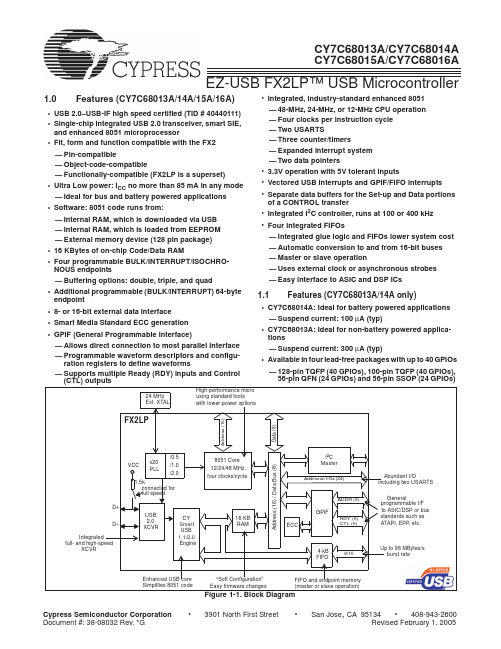
• CY7C68016A: Ideal for battery powered applications — Suspend current: 100 µA (typ) • CY7C68015A: Ideal for non-battery powered applications — Suspend current: 300 µA (typ) • Available in lead-free 56-pin QFN package (26 GPIOs) — 2 more GPIOs than CY7C68013A/14A enabling additional features in same footprint Cypress Semiconductor Corporation’s (Cypress’s) EZ-USB FX2LP (CY7C68013A/14A) is a low-power version of the EZ-USB FX2 (CY7C68013), which is a highly integrated, low-power USB 2.0 microcontroller. By integrating the USB 2.0 transceiver, serial interface engine (SIE), enhanced 8051 microcontroller, and a programmable peripheral interface in a single chip, Cypress has created a very cost-effective solution that provides superior time-to-market advantages with low power to enable bus powered applications. The ingenious architecture of FX2LP results in data transfer rates of over 53 Mbytes per second, the maximum-allowable USB 2.0 bandwidth, while still using a low-cost 8051 microcontroller in a package as small as a 56 QFN. Because it incorporates the USB 2.0 transceiver, the FX2LP is more economical, providing a smaller footprint solution than USB 2.0 SIE or external transceiver implementations. With EZ-USB FX2LP, the Cypress Smart SIE handles most of the USB 1.1 and 2.0 protocol in hardware, freeing the embedded microcontroller for application-specific functions and decreasing development time to ensure USB compatibility. The General Programmable Interface (GPIF) and Master/Slave Endpoint FIFO (8- or 16-bit data bus) provides
CY7C67300-100AI资料

CY7C67300 EZ-Host™ Programmable EmbeddedUSB Host/Peripheral ControllerTABLE OF CONTENTS1.0 INTRODUCTION (10)1.1 EZ-Host Features (10)2.0 TYPICAL APPLICATIONS (11)3.0 FUNCTIONAL OVERVIEW (11)3.1 Processor Core (11)3.1.1 Processor (11)3.1.2 Clocking (11)3.1.3 Memory (11)3.1.4 Interrupts (11)3.1.5 General Timers and Watchdog Timer (11)3.1.6 Power Management (11)4.0 INTERFACE DESCRIPTIONS (11)4.1 USB Interface (13)4.1.1 USB Features (13)4.1.2 USB Pins. (14)4.2 OTG Interface (14)4.2.1 OTG Features (14)4.2.2 OTG Pins. (14)4.3 External Memory Interface (14)4.3.1 External Memory Interface Features (14)4.3.2 External Memory Access Strobes (14)4.3.3 Page Registers (15)4.3.4 Merge Mode (15)4.3.5 Program Memory Hole Description (15)4.3.6 DMA to External Memory Prohibited (15)4.3.7 External Memory Interface Pins (16)4.3.8 External Memory Interface Block Diagrams (17)4.4 General Purpose I/O Interface (GPIO) (18)4.4.1 GPIO Description (18)4.4.2 Unused Pin Descriptions (18)4.5 UART Interface (18)4.5.1 UART Features (18)4.5.2 UART Pins. (18)4.6 I2C EEPROM Interface (18)4.6.1 I2C EEPROM Features (18)4.6.2 I2C EEPROM Pins. (18)4.7 Serial Peripheral Interface (18)4.7.1 SPI Features (19)4.7.2 SPI Pins (19)4.8 High-speed Serial Interface (19)4.8.1 HSS Features (19)4.8.2 HSS Pins (20)4.9 Programmable Pulse/PWM Interface (20)4.9.1 Programmable Pulse/PWM Features (20)4.9.2 Programmable Pulse/PWM Pins. (20)4.10 Host Port Interface (20)4.10.1 HPI Features (20)4.10.2 HPI Pins. (21)TABLE OF CONTENTS (continued)4.11 IDE Interface (21)4.11.1 IDE Features (22)4.11.2 IDE Pins (22)4.12 Charge Pump Interface (22)4.12.1 Charge Pump Features (23)4.12.2 Charge Pump Pins. (23)4.13 Booster Interface (23)4.13.1 Booster Pins. (24)4.14 Crystal Interface (25)4.14.1 Crystal Pins (25)4.15 Boot Configuration Interface (25)4.16 Operational Modes (26)4.16.1 Coprocessor Mode (26)4.16.2 Standalone Mode (26)5.0 POWER-SAVINGS AND RESET DESCRIPTION (27)5.1 Power-Savings Mode Description (27)5.2 Sleep (27)5.3 External (Remote) wakeup Source (27)5.4 Power-On-Reset Description (27)5.5 Reset Pin (27)5.6 USB Reset (27)6.0 MEMORY MAP (28)6.1 Mapping (28)6.1.1 Internal Memory (28)6.1.2 External Memory (28)7.0 REGISTERS (30)7.1 Processor Control Registers (30)7.1.1 CPU Flags Register [0xC000] [R] (30)7.1.2 Bank Register [0xC002] [R/W] (31)7.1.3 Hardware Revision Register [0xC004] [R] (31)7.1.4 CPU Speed Register [0xC008] [R/W] (32)7.1.5 Power Control Register [0xC00A] [R/W] (33)7.1.6 Interrupt Enable Register [0xC00E] [R/W] (35)7.1.7 Breakpoint Register [0xC014] [R/W] (36)7.1.8 USB Diagnostic Register [0xC03C] [R/W] (37)7.1.9 Memory Diagnostic Register [0xC03E] [W] (38)7.2 External Memory Registers (39)7.2.1 Extended Page n Map Register [R/W] (39)7.2.2 Upper Address Enable Register [0xC038] [R/W] (39)7.2.3 External Memory Control Register [0xC03A] [R/W] (40)7.3 Timer Registers (41)7.3.1 Watchdog Timer Register [0xC00C] [R/W] (41)7.3.2 Timer n Register [R/W] (42)7.4 General USB Registers (42)7.4.1 USB n Control Register [R/W] (42)7.5 USB Host Only Registers (45)7.5.1 Host n Control Register [R/W] (45)7.5.2 Host n Address Register [R/W] (46)TABLE OF CONTENTS (continued)7.5.3 Host n Count Register [R/W] (46)7.5.4 Host n Endpoint Status Register [R] (47)7.5.5 Host n PID Register [W] (48)7.5.6 Host n Count Result Register [R] (49)7.5.7 Host n Device Address Register [W] (50)7.5.8 Host n Interrupt Enable Register [R/W] (50)7.5.9 Host n Status Register [R/W] (52)7.5.10 Host n SOF/EOP Count Register [R/W] (53)7.5.11 Host n SOF/EOP Counter Register [R] (53)7.5.12 Host n Frame Register [R] (54)7.6 USB Device Only Registers (54)7.6.1 Device n Endpoint n Control Register [R/W] (55)7.6.2 Device n Endpoint n Address Register [R/W] (56)7.6.3 Device n Endpoint n Count Register [R/W] (57)7.6.4 Device n Endpoint n Status Register [R/W] (57)7.6.5 Device n Endpoint n Count Result Register [R/W] (59)7.6.6 Device n Port Select Register [R/W] (60)7.6.7 Device n Interrupt Enable Register [R/W] (60)7.6.8 Device n Address Register [W] (63)7.6.9 Device n Status Register [R/W] (63)7.6.10 Device n Frame Number Register [R] (65)7.6.11 Device n SOF/EOP Count Register [W] (66)7.7 OTG Control Registers (66)7.7.1 OTG Control Register [0xC098] [R/W] (66)7.8 GPIO Registers (68)7.8.1 GPIO Control Register [0xC006] [R/W] (68)7.8.2 GPIO n Output Data Register [R/W] (70)7.8.3 GPIO n Input Data Register [R] (70)7.8.4 GPIO n Direction Register [R/W] (71)7.9 IDE Registers (71)7.9.1 IDE Mode Register [0xC048] [R/W] (71)7.9.2 IDE Start Address Register [0xC04A] [R/W] (72)7.9.3 IDE Stop Address Register [0xC04C] [R/W] (72)7.9.4 IDE Control Register [0xC04E] [R/W] (73)7.9.5 IDE PIO Port Registers [0xC050 - 0xC06F] [R/W] (74)7.10 HSS Registers (74)7.10.1 HSS Control Register [0xC070] [R/W] (75)7.10.2 HSS Baud Rate Register [0xC072] [R/W] (77)7.10.3 HSS Transmit Gap Register [0xC074] [R/W] (77)7.10.4 HSS Data Register [0xC076] [R/W] (78)7.10.5 HSS Receive Address Register [0xC078] [R/W] (78)7.10.6 HSS Receive Counter Register [0xC07A] [R/W] (79)7.10.7 HSS Transmit Address Register [0xC07C] [R/W] (79)7.10.8 HSS Transmit Counter Register [0xC07E] [R/W] (79)7.11 HPI Registers (80)7.11.1 HPI Breakpoint Register [0x0140] [R] (80)7.11.2 Interrupt Routing Register [0x0142] [R] (81)7.11.3 SIEXmsg Register [W] (82)7.11.4 HPI Mailbox Register [0xC0C6] [R/W] (83)7.11.5 HPI Status Port [] [HPI: R] (83)TABLE OF CONTENTS (continued)7.12 SPI Registers (85)7.12.1 SPI Configuration Register [0xC0C8] [R/W] (86)7.12.2 SPI Control Register [0xC0CA] [R/W] (87)7.12.3 SPI Interrupt Enable Register [0xC0CC] [R/W] (89)7.12.4 SPI Status Register [0xC0CE] [R] (89)7.12.5 SPI Interrupt Clear Register [0xC0D0] [W] (90)7.12.6 SPI CRC Control Register [0xC0D2] [R/W] (91)7.12.7 SPI CRC Value Register [0xC0D4] [R/W] (92)7.12.8 SPI Data Register [0xC0D6] [R/W] (92)7.12.9 SPI Transmit Address Register [0xC0D8] [R/W] (93)7.12.10 SPI Transmit Count Register [0xC0DA] [R/W] (93)7.12.11 SPI Receive Address Register [0xC0DC [R/W] (93)7.12.12 SPI Receive Count Register [0xC0DE] [R/W] (94)7.13 UART Registers (94)7.13.1 UART Control Register [0xC0E0] [R/W] (94)7.13.2 UART Status Register [0xC0E2] [R] (95)7.13.3 UART Data Register [0xC0E4] [R/W] (96)7.14 PWM Registers (96)7.14.1 PWM Control Register [0xC0E6] [R/W] (97)7.14.2 PWM Maximum Count Register [0xC0E8] [R/W] (98)7.14.3 PWM n Start Register [R/W] (99)7.14.4 PWM n Stop Register [R/W] (99)7.14.5 PWM Cycle Count Register [0xC0FA] [R/W] (100)8.0 PIN DIAGRAM (101)9.0 PIN DESCRIPTIONS (101)10.0 ABSOLUTE MAXIMUM RATINGS (105)11.0 OPERATING CONDITIONS (105)12.0 CRYSTAL REQUIREMENTS (XTALIN, XTALOUT) (105)13.0 DC CHARACTERISTICS (105)13.1 USB Transceiver (106)14.0 AC TIMING CHARACTERISTICS (107)14.1 Reset Timing (107)14.2 Clock Timing (107)14.3 SRAM Read Cycle (108)14.4 SRAM Write Cycle (109)14.5 I2C EEPROM Timing (110)14.6 HPI (Host Port Interface) Write Cycle Timing (111)14.7 HPI (Host Port Interface) Read Cycle Timing (112)14.8 IDE Timing (113)14.9 HSS BYTE Mode Transmit (113)14.10 HSS Block Mode Transmit (113)14.11 HSS BYTE and BLOCK Mode Receive (113)14.12 Hardware CTS/RTS Handshake (114)15.0 REGISTERS SUMMARY (114)16.0 ORDERING INFORMATION (118)17.0 PACKAGE DIAGRAMS (118)LIST OF FIGURESFigure 1-1. Block Diagram (10)Figure 4-1. Page n Registers External Address Pins Logic (15)Figure 4-2. Interfacing to 64k × 8 Memory Array (17)Figure 4-3. Interfacing up to 256k × 16 for External Code/Data (17)Figure 4-4. Interfacing up to 512k × 8 for External Code/Data (17)Figure 4-5. Charge Pump (23)Figure 4-6. Power Supply Connection With Booster (24)Figure 4-7. Power Supply Connection Without Booster (24)Figure 4-8. Crystal Interface (25)Figure 4-9. Minimum Standalone Hardware Configuration – Peripheral Only (26)Figure 6-1. Memory Map (29)Figure 7-1. Processor Control Registers (30)Figure 7-2. CPU Flags Register (30)Figure 7-3. Bank Register (31)Figure 7-4. Revision Register (31)Figure 7-5. CPU Speed Register (32)Figure 7-6. Power Control Register (33)Figure 7-7. Interrupt Enable Register (35)Figure 7-8. Breakpoint Register (36)Figure 7-9. USB Diagnostic Register (37)Figure 7-10. Memory Diagnostic Register (38)Figure 7-11. External Memory Control Registers (39)Figure 7-12. Extended Page n Map Register (39)Figure 7-13. External Memory Control Register (39)Figure 7-14. External Memory Control Register (40)Figure 7-15. Timer Registers (41)Figure 7-16. Watchdog Timer Register (41)Figure 7-17. Timer n Register (42)Figure 7-18. General USB Registers (42)Figure 7-19. USB n Control Register (43)Figure 7-20. USB Host Only Register (45)Figure 7-21. Host n Control Register (45)Figure 7-22. Host n Address Register (46)Figure 7-23. Host n Count Register (46)Figure 7-24. Host n Endpoint Status Register (47)Figure 7-25. Host n PID Register (49)Figure 7-26. Host n Count Result Register (49)Figure 7-27. Host n Device Address Register (50)Figure 7-28. Host n Interrupt Enable Register (50)Figure 7-29. Host n Status Register (52)Figure 7-30. Host n SOF/EOP Count Register (53)Figure 7-31. Host n SOF/EOP Counter Register (54)Figure 7-32. Host n Frame Register (54)Figure 7-33. USB Device Only Registers (55)Figure 7-34. Device n Endpoint n Control Register (55)Figure 7-35. Device n Endpoint n Address Register (57)Figure 7-36. Device n Endpoint n Count Register (57)Figure 7-37. Device n Endpoint n Status Register (58)Figure 7-38. Device n Endpoint n Count Result Register (60)LIST OF FIGURES (continued)Figure 7-39. Device n Port Select Register (60)Figure 7-40. Device n Interrupt Enable Register (61)Figure 7-41. Device n Address Register (63)Figure 7-42. Device n Status Register (63)Figure 7-43. Device n Frame Number Register (65)Figure 7-44. Device n SOF/EOP Count Register (66)Figure 7-45. OTG Registers (66)Figure 7-46. OTG Control Register (66)Figure 7-47. GPIO Registers (68)Figure 7-48. GPIO Control Register (68)Figure 7-49. GPIO n Output Data Register (70)Figure 7-50. GPIO n Input Data Register (70)Figure 7-51. GPIO n Direction Register (71)Figure 7-52. IDE Registers (71)Figure 7-53. IDE Mode Register (71)Figure 7-54. IDE Start Address Register (72)Figure 7-55. IDE Stop Address Register (72)Figure 7-56. IDE Control Register (73)Figure 7-57. HSS Registers (74)Figure 7-58. HSS Control Register (75)Figure 7-59. HSS Baud Rate Register (77)Figure 7-60. HSS Transmit Gap Register (77)Figure 7-61. HSS Data Register (78)Figure 7-62. HSS Receive Address Register (78)Figure 7-63. HSS Receive Counter Register (79)Figure 7-64. HSS Transmit Address Register (79)Figure 7-65. HSS Transmit Counter Register (79)Figure 7-66. HPI Registers (80)Figure 7-67. HPI Breakpoint Register (80)Figure 7-68. Interrupt Routing Register (81)Figure 7-69. SIEXmsg Register (82)Figure 7-70. HPI Mailbox Register (83)Figure 7-71. HPI Status Port (83)Figure 7-72. SPI Registers (85)Figure 7-73. SPI Configuration Register (86)Figure 7-74. SPI Control Register (87)Figure 7-75. SPI Interrupt Enable Register (89)Figure 7-76. SPI Status Register (89)Figure 7-77. SPI Interrupt Clear Register (90)Figure 7-78. SPI CRC Control Register (91)Figure 7-79. SPI CRC Value Register (92)Figure 7-80. SPI Data Register (92)Figure 7-81. SPI Transmit Address Register (93)Figure 7-82. SPI Transmit Count Register (93)Figure 7-83. SPI Receive Address Register (93)Figure 7-84. SPI Receive Count Register (94)Figure 7-85. UART Registers (94)Figure 7-86. UART Control Register (94)Figure 7-87. UART Status Register (95)LIST OF FIGURES (continued)Figure 7-88. UART Data Register (96)Figure 7-89. PWM Registers (96)Figure 7-90. PWM Control Register (97)Figure 7-91. PWM Maximum Count Register (98)Figure 7-92. PWM n Start Register (99)Figure 7-93. PWM n Stop Register (99)Figure 7-94. PWM Cycle Count Register (100)Figure 8-1. EZ-Host Pin Diagram (101)LIST OF TABLESTable 4-1. Interface Options for GPIO Pins (12)Table 4-2. Interface Options for External Memory Bus Pins (12)Table 4-3. USB Port Configuration Options (13)Table 4-4. USB Interface Pins (14)Table 4-5. OTG Interface Pins (14)Table 4-6. External Memory Interface Pins (16)Table 4-7. UART Interface Pins (18)Table 4-8. I2C EEPROM Interface Pins (18)Table 4-9. SPI Interface Pins (19)Table 4-10. HSS Interface Pins (20)Table 4-11. PWM Interface Pins (20)Table 4-12. HPI Interface Pins (21)Table 4-13. HPI Addressing (21)Table 4-14. IDE Throughput (22)Table 4-15. IDE Interface Pins (22)Table 4-16. Charge Pump Interface Pins (23)Table 4-17. Charge Pump Interface Pins (24)Table 4-18. Crystal Pins (25)Table 4-19. Boot Configuration Interface (25)Table 5-1. Wakeup Sources (27)Table 7-1. Bank Register Example (31)Table 7-2. CPU Speed Definition (32)Table 7-3. Force Select Definition (38)Table 7-4. Memory Arbitration Select (38)Table 7-5. Period Select Definition (41)Table 7-6. USB Data Line Pull-up and Pull-down Resistors (44)Table 7-7. Port A/B Force D± State (44)Table 7-8. Port Select Definition (47)Table 7-9. PID Select Definition (49)Table 7-10. Mode Select Definition (69)Table 7-11. Mode Select Definition (72)Table 7-12. IDE PIO Port Registers (74)Table 7-13. Scale Select Field Definition for SCK Frequency (86)Table 7-14. CRC Mode Definition (91)Table 7-15. UART Baud Select Definition (95)Table 7-16. Prescaler Select Definition (97)Table 9-1. Pin Descriptions (101)Table 12-1. Crystal Requirements (105)Table 13-1. DC Characteristics (105)Table 13-2. DC Characteristics: Charge Pump (106)Table 15-1. Register Summary (114)Table 16-1. Ordering Information (118)1.0 INTRODUCTIONEZ-Host™ (CY7C67300) is Cypress Semiconductor’s first full-speed, low-cost multiport host/peripheral controller. EZ-Host is designed to easily interface to most high-performance CPUs to add USB host functionality. EZ-Host has its own 16-bit RISC processor to act as a coprocessor or operate in standalone mode. EZ-Host also has a programmable I/O interface block allowing a wide range of interface options.Figure 1-1. Block Diagram1.1EZ-Host Features•Single-chip programmable USB dual-role (Host/Peripheral) controller with two configurable Serial Interface Engines (SIEs) and four USB ports•Support for USB On-The-Go (OTG) protocol•On-chip 48-MHz 16-bit processor with dynamically switchable clock speed•Configurable I/O block supporting a variety of I/O options or up to 32 bits of General Purpose I/O (GPIO)•4K x 16 internal masked ROM containing built-in BIOS that supports a communication ready state with access to I2C EEPROM Interface, external ROM, UART, or USB•8K x 16 internal RAM for code and data buffering•Extended memory interface port for external SRAM and ROM•16-bit parallel Host Port Interface (HPI) with a DMA/Mailbox data path for an external processor to directly access all of the on-chip memory and control on-chip SIEs•Fast serial port supports from 9600 baud to 2.0 Mbaud•SPI support in both master and slave•On-chip 16-bit DMA/Mailbox data path interface•Supports 12-MHz external crystal or clock•3.3V operation•Package option — 100-pin TQFP2.0 Typical ApplicationsEZ-Host is a very powerful and flexible dual role USB controller that supports a wide variety of applications. It is primarily intended to enable host capability in applications such as:•Set-top boxes•Printers•KVM switches•Kiosks•Automotive applications•Wireless access points.3.0 Functional Overview3.1Processor Core3.1.1ProcessorEZ-Host has a general-purpose 16-bit embedded RISC processor that runs at 48 MHz.3.1.2ClockingEZ-Host requires a 12-MHz source for clocking. Either an external crystal or TTL level oscillator may be used. EZ-Host has an internal PLL that produces a 48-MHz internal clock from the 12-MHz source.3.1.3MemoryEZ-Host has a built-in 4K × 16 masked ROM and an 8K × 16 internal RAM. The masked ROM contains the EZ-Host BIOS. The internal RAM can be used for program code or data.3.1.4InterruptsEZ-Host provides 128 interrupt vectors. The first 48 vectors are hardware interrupts and the following 80 vectors are software interrupts.3.1.5General Timers and Watchdog TimerEZ-Host has two built-in programmable timers and a Watchdog timer. All three timers can generate an interrupt to the EZ-Host.3.1.6Power ManagementEZ-Host has one main power saving mode, Sleep. Sleep mode pauses all operations and provides the lowest power state.4.0 Interface DescriptionsEZ-Host has a wide variety of interface options for connectivity. With several interface options available, EZ-Host can act as a seamless data transport between many different types of devices.See Table4-1 and Table4-2 to understand how the interfaces share pins and which can coexist. It should be noted that some interfaces have more then one possible port location selectable through the GPIO Control Register [0xC006]. Below are some general guidelines:•HPI and IDE interfaces are mutually exclusive.•If 16-bit external memory is required, then HSS and SPI default locations must be used.•I2C EEPROM and OTG do not conflict with any interfaces.Notes:1.Default interface location.2.Alternate interface location.Table 4-1. Interface Options for GPIO Pins GPIO Pins HPIIDEPWMHSSSPIUARTI2C OTGGPIO31SCL/SDA GPIO30SCL/SDAGPIO29OTGIDGPIO28TX [1]GPIO27RX [1]GPIO26PWM3CTS [1]GPIO25GPIO24INT IOREADY GPIO23nRD IOR GPIO22nWR IOW GPIO21nCS GPIO20A1CS1GPIO19A0CS0GPIO18A2PWM2RTS [1]GPIO17A1PWM1RXD [1]GPIO16A0PWM0TXD [1]GPIO15D15D15GPIO14D14D14GPIO13D13D13GPIO12D12D12GPIO11D11D11MOSI [1]GPIO10D10D10SCK [1]GPIO9D9D9nSSI [1]GPIO8D8D8MISO [1]GPIO7D7D7TX [2]GPIO6D6D6RX [2]GPIO5D5D5GPIO4D4D4GPIO3D3D3GPIO2D2D2GPIO1D1D1GPIO0D0D0Table 4-2. Interface Options for External Memory Bus Pins MEM Pins HPIIDEPWMHSS SPIUARTI2COTGD15CTS [2]D14RTS [2]D13RXD [2]D12TXD [2]D11MOSI [2]D10SCK [2]D9nSSI [2]D8MISO [2]D[7:0]A[18:0]CONTROL4.1USB InterfaceEZ-Host has two built-in Host/Peripheral SIEs and four USB transceivers that meet the USB 2.0 specification requirements for full and low speed (high speed is not supported). In Host mode, EZ-Host supports four downstream ports, each support control, interrupt, bulk, and isochronous transfers. In Peripheral mode, EZ-Host supports one peripheral port with eight endpoints for each of the two SIEs. Endpoint 0 is dedicated as the control endpoint and only supports control transfers. Endpoints 1 though 7 support Interrupt, Bulk (up to 64 Bytes/packet), or Isochronous transfers (up to 1023 Bytes/packet size). EZ-Host also supports a combi-nation of Host and Peripheral ports simultaneously as shown in Table4-3.Table 4-3. USB Port Configuration OptionsPort Configurations Port 1A Port 1B Port 2A Port 2BOTG OTG–––OTG + 2 Hosts OTG–Host HostOTG + 1 Host OTG–Host–OTG + 1 Host OTG––HostOTG + 1 Peripheral OTG–Peripheral–OTG + 1 Peripheral OTG––Peripheral4 Hosts Host Host Host Host3 Hosts Any Combination of Ports2 Hosts Any Combination of Ports1 Host Any Port2 Hosts + 1 Peripheral Host Host Peripheral–2 Hosts + 1 Peripheral Host Host–Peripheral2 Hosts + 1 Peripheral Peripheral–Host Host2 Hosts + 1 Peripheral–Peripheral Host Host1 Host + 1 Peripheral Host–Peripheral–1 Host + 1 Peripheral Host––Peripheral1 Host + 1 Peripheral–Host–Peripheral1 Host + 1 Peripheral–Host Peripheral–1 Host + 1 Peripheral Peripheral–Host–1 Host + 1 Peripheral Peripheral––Host1 Host + 1 Peripheral–Peripheral–Host1 Host + 1 Peripheral–Peripheral Host–2 Peripherals Peripheral–Peripheral–2 Peripherals Peripheral––Peripheral2 Peripherals–Peripheral–Peripheral2 Peripherals–Peripheral Peripheral–1 Peripheral Any Port4.1.1USB Features•USB 2.0-compliant for full and low speed•Up to four downstream USB host ports•Up to two upstream USB peripheral ports•Configurable endpoint buffers (pointer and length), must reside in internal RAM•Up to eight available peripheral endpoints (one control endpoint)•Supports Control, Interrupt, Bulk, and Isochronous transfers•Internal DMA channels for each endpoint•Internal pull-up and pull-down resistors•Internal Series termination resistors on USB data lines4.1.2USB Pins.Table 4-4. USB Interface PinsPin Name Pin NumberDM1A22DP1A23DM1B18DP1B19DM2A9DP2A10DM2B4DP2B54.2OTG InterfaceEZ-Host has one USB port that is compatible with the USB On-The-Go supplement to the USB 2.0 specification. The USB OTG port has a various hardware features to support Session Request Protocol (SRP) and Host Negotiation Protocol (HNP). OTG is only supported on USB PORT 1A.4.2.1OTG Features•Internal Charge Pump to supply and control VBUS•VBUS Valid Status (above 4.4V)•VBUS Status for 2.4V< VBUS <0.8V•ID Pin Status•Switchable 2KΩ internal discharge resistor on VBUS•Switchable 500Ω internal Pull-up resistor on VBUS•Individually switchable internal Pull-up and Pull-down resistors on the USB Data Lines4.2.2OTG Pins.Table 4-5. OTG Interface PinsPin Name Pin NumberDM1A22DP1A23OTGVBUS11OTGID41CSwitchA13CSwitchB124.3External Memory InterfaceEZ-Host provides a robust interface to a wide variety of external memory arrays. All available external memory array locations can contain either code or data. The CY16 RISC processor directly addresses a flat memory space from 0x0000 to 0xFFFF. 4.3.1External Memory Interface Features•Supports 8-bit or 16-bit SRAM or ROM•SRAM or ROM can be used for code or data space•Direct addressing of SRAM or ROM•Two external memory mapped page registers4.3.2External Memory Access StrobesAccess to external memory is sampled asynchronously on the rising edge of strobes with a minimum of one wait state cycle. Up to seven wait state cycles may be inserted for external memory access. Each additional wait state cycle stretches the external memory access time by 21 nsec. An external memory device with 12-nsec access time is necessary to support 48-MHz code execution.4.3.3Page RegistersEZ-Host allows extended data or program code to be stored in external SRAM, or ROM. The total size of extended memory can be up to 512K bytes. The CY16 processor can access extended memory via two address regions of 0x8000-0x9FFF and 0xA000-0xBFFF. The page register 0xC018 can be used to control the address region 0x8000-0x9FFF and the page register 0xC01A controls the address region of 0xA000-0xBFFF.Figure4-1 illustrates that when the nXMEMSEL pin is asserted the upper CPU address pins are driven by the contents of the Page x Registers.Figure 4-1. Page n Registers External Address Pins Logic4.3.4Merge ModeMerge modes enabled through the External Memory Control Register [0xC03] allow combining of external memory regions in accordance with the following:•nXMEMSEL is active from 0x8000 to 0xBFFF•nXRAMSEL is active from 0x4000 to 0x7FFF when RAM Merge is disabled; nXRAMSEL is active from 0x4000 to 0xBFFF when RAM Merge is enabled•nXROMSEL is active from 0xC100 to 0xDFFF when ROM Merge is disabled; nXROMSEL is active from 0x8000 to 0xDFFF (excluding the 0xC000 to 0xC0FF area) when ROM Merge is enabled4.3.5Program Memory Hole DescriptionCode residing in the 0xC000-0xC0FF address space is not accessible by the cpu.4.3.6DMA to External Memory ProhibitedEZ-Host supports an internal DMA engine to rapidly move data between different functional blocks within the chip. This DMA engine is used for SIE1, SIE2, HPI, SPI, HSS, and IDE but it can only transfer data between the specified block and internal RAM or ROM. Setting up the DMA engine to transfer to or from an external memory space might result in internal RAM data corruption because the hardware (i.e HSS/HPI/SIE1/SIE2/IDE) does not explicitly check the address range. For example, setting up a DMA transfer to external address 0x8000 might result in a DMA transfer into address 0x0000.External Memory Related Resource Considerations:•By default A[18:15] are not available for general addressing and are driven high on power up. The Upper Address Enable Register must be written appropriately to enable A[18:15] for general addressing purposes.•47k ohm external pull-up on A15-pin for 12-MHz crystal operation.•During the 3-msec BIOS boot procedure the CPU external memory bus is active.•ROM boot load value 0xC3B6 located at 0xC100.•HPI, HSS, SPI, SIE1, SIE2, and IDE can't DMA to external memory arrays.•Page 1 banking is always enabled and is in effect from 0x8000 to 0x9FFF.•Page 2 banking is always enabled and is in effect from 0xA000 to 0xBFFF.•CPU memory bus strobes may wiggle when chip selects are inactive.4.3.7External Memory Interface PinsTable 4-6. External Memory Interface PinsPin Name Pin Number nWR64nRD62 nXMEMSEL (optional nCS)34nXROMSEL (ROM nCS)35nXRAMSEL (RAM nCS)36A1896A1795A1697A1538A1433A1332A1231A1130A1027A925A824A720A617A58A47A33A22A11nBEL/A099nBEH98D1567D1468D1369D1270D1171D1072D973D874D776D677D578D479D380D281D182D0834.3.8External Memory Interface Block DiagramsFigure4-2 illustrates how to connect a 64k × 8 memory array (SRAM/ROM) to the EZ-Host external memory interface.Figure 4-2. Interfacing to 64k × 8 Memory ArrayFigure4-3 illustrates the interface for connecting a 16-bit ROM or 16-bit RAM to the EZ-Host external memory interface. In 16-bit mode, up to 256K words of external ROM or RAM are supported. Note that the Address lines do not map directly.Figure 4-3. Interfacing up to 256k × 16 for External Code/DataFigure4-4 illustrates the interface for connecting an 8-bit ROM or 8-bit RAM to the EZ-Host external memory interface. In 8-bit mode, up to 512K bytes of external ROM or RAM are supported.Figure 4-4. Interfacing up to 512k × 8 for External Code/Data4.4General Purpose I/O Interface (GPIO)EZ-Host has up to 32 GPIO signals available. Several other optional interfaces use GPIO pins as well and may reduce the overall number of available GPIOs.4.4.1GPIO DescriptionAll Inputs are sampled asynchronously with state changes occurring at a rate of up to two 48-MHZ clock cycles. GPIO pins are latched directly into registers, a single flip-flop.4.4.2Unused Pin DescriptionsUnused USB pins should be three-stated with the D+ line pulled high through the internal pull-up resistor and the D- line pulled low through the internal pull-down resistor.Unused GPIO pins should be configured as outputs and driven low.4.5UART InterfaceEZ-Host has a built-in UART interface. The UART interface supports data rates from 900 to 115.2K baud. It can be used as a development port or for other interface requirements. The UART interface is exposed through GPIO pins.4.5.1UART Features•Supports baud rates of 900 to 115.2K•8-N-14.5.2UART Pins.Table 4-7. UART Interface PinsPin Name Pin NumberTX42RX434.6I2C EEPROM InterfaceEZ-Host provides a master only I2C interface for external serial EEPROMs. The serial EEPROM can be used to store application specific code and data. This I2C interface is only to be used for loading code out of EEPROM, it is not a general I2C interface. The I2C EEPROM interface is a BIOS implementation and is exposed through GPIO pins. Please refer to the BIOS documentation for additional details on this interface.4.6.1I2C EEPROM Features•Supports EEPROMs up to 64KB (512K bit)•Auto-detection of EEPROM size4.6.2I2C EEPROM Pins.Table 4-8. I2C EEPROM Interface PinsPin Name Pin NumberSMALL EEPROMSCK39SDA40LARGE EEPROMSCK40SDA394.7Serial Peripheral InterfaceEZ-Host provides a SPI interface for added connectivity. EZ-Host may be configured as either an SPI master or SPI slave. The SPI interface can be exposed through GPIO pins or the External Memory port.。
- 1、下载文档前请自行甄别文档内容的完整性,平台不提供额外的编辑、内容补充、找答案等附加服务。
- 2、"仅部分预览"的文档,不可在线预览部分如存在完整性等问题,可反馈申请退款(可完整预览的文档不适用该条件!)。
- 3、如文档侵犯您的权益,请联系客服反馈,我们会尽快为您处理(人工客服工作时间:9:00-18:30)。
PRELIMINARY 4-Mbit (128K x 36) Pipelined SRAMwith NoBL™ ArchitectureCY7C1350GFeatures•Pin compatible and functionally equivalent to ZBT™ devices•Internally self-timed output buffer control to eliminate the need to use OE •Byte Write capability•128K x 36 common I/O architecture •Single 3.3V power supply •2.5V/3.3V I/O Operation •Fast clock-to-output times —2.6 ns (for 250-MHz device)—2.6 ns (for 225-MHz device)—2.8 ns (for 200-MHz device)—3.5 ns (for 166-MHz device)—4.0 ns (for 133-MHz device)—4.5 ns (for 100-MHz device)•Clock Enable (CEN) pin to suspend operation •Synchronous self-timed writes •Asynchronous output enable (OE)•Lead-Free 100 TQFP and 119 BGA packages•Burst Capability—linear or interleaved burst orderFunctional Description [1]The CY7C1350G is a 3.3V, 128K x 36 synchronous-pipelined Burst SRAM designed specifically to support unlimited true back-to-back Read/Write operations without the insertion of wait states. The CY7C1350G is equipped with the advanced No Bus Latency™ (NoBL™) logic required to enable consec-utive Read/Write operations with data being transferred on every clock cycle. This feature dramatically improves the throughput of the SRAM, especially in systems that require frequent Write/Read transitions.All synchronous inputs pass through input registers controlled by the rising edge of the clock. All data outputs pass through output registers controlled by the rising edge of the clock. The clock input is qualified by the Clock Enable (CEN) signal,which, when deasserted, suspends operation and extends the previous clock cycle. Maximum access delay from the clock rise is 2.6 ns (250-MHz device)Write operations are controlled by the four Byte Write Select (BW [A:D]) and a Write Enable (WE) input. All writes are conducted with on-chip synchronous self-timed write circuitry.Three synchronous Chip Enables (CE 1, CE 2, CE 3) and an asynchronous Output Enable (OE) provide for easy bank selection and output tri-state control. In order to avoid bus contention, the output drivers are synchronously tri-stated during the data portion of a write sequence.1.For best-practices recommendations, please refer to the Cypress application note System Design Guidelines on .Selection Guide250 MHz225 MHz 200 MHz 166 MHz 133 MHz 100 MHz Unit Maximum Access Time 2.6 2.6 2.8 3.5 4.0 4.5ns Maximum Operating Current 325290265240225205mA Maximum CMOS Standby Current404040404040mAShaded area contains advance information. Please contact your local Cypress sales representative for availability of these parts.Pin ConfigurationAAAAA 1A 0N C / 288MN C / 144MV S SV D DN C / 36MAAAAAA DQPB DQ B DQ B V DDQ V SS DQ B DQ B DQ B DQ B V SS V DDQ DQ B DQ B V SS NC V DD DQ A DQ A V DDQ V SS DQ A DQ A DQ A DQ A V SS V DDQ DQ A DQ A DQP ADQP C DQ C DQ C V DDQ V SSDQ C DQ C DQ C DQ C V SS V DDQ DQ C DQ C NC V DD NC V SS DQ D DQ D V DDQ V SS DQ DDQ D DQ D DQ D V SS V DDQ DQ D DQ D DQP DAAC E 1C E 2B W DB W CB W BB W AC E 3V D DV S SC L KW EC E NO EA A123456789101112131415161718192021222324252627282930313233343536373839404142434445464748495080797877767574737271706968676665646362616059585756555453525110099989796959493929190898887868584838281AA D V /L DZZ M O D EN C / 72MN C / 18M N C / 9MCY7C1350G100-Pin TQFPBYTE BBYTE A BYTE CBYTE DPin Configuration (continued)2345671ABCDEFGHJKLMNP R T UDQ A V DDQNCNCDQ CDQ DDQ CDQ DA A A ANC / 18M V DDQ CE2AV DDQV DDQV DDQV DDQNCNCADQ CDQ CDQ DDQ DNCV DDANC / 72MDQP DAAADV/LD A CE3NCV DD A A NCV SS V SSNC DQP BDQ BDQ BDQ ADQ BDQ BDQ ADQ ANCNC NC V DDQNCV SSV SSV SSV SSV SSV SSV SSV SSMODECE1V SSOE V SS V DDQBW C NC / 9MV SSWEV DDQV DD V SS V DDV SSCLKNC BW ACEN V SS V DDQV SSZZNCAAA1A0V SSV DDDQP C DQ BA NC / 36MDQ C DQ BDQ CDQ CDQ CDQ BDQ BDQ ADQ ADQ ADQ ADQP ADQ DDQ DDQ DDQ DBW D119-Ball Bump BGABW BNCPin DefinitionsName I/O DescriptionA0, A1, A Input-Synchronous Address Inputs used to select one of the 128K address locations. Sampled at the rising edge of the CLK. A[1:0] are fed to the two-bit burst counter.BW[A:D]Input-Synchronous Byte Write Inputs, active LOW. Qualified with WE to conduct writes to the SRAM. Sampled on the rising edge of CLK.WE Input-Synchronous Write Enable Input, active LOW. Sampled on the rising edge of CLK if CEN is active LOW. This signal must be asserted LOW to initiate a write sequence.ADV/LD Input-Synchronous Advance/Load Input. Used to advance the on-chip address counter or load a new address. When HIGH (and CEN is asserted LOW) the internal burst counter is advanced. When LOW, a new address can be loaded into the device for an access. After being deselected, ADV/LD should be driven LOW in order to load a new address.CLK Input-Clock Clock Input. Used to capture all synchronous inputs to the device. CLK is qualified with CEN.CLK is only recognized if CEN is active LOW.CE1Input-Synchronous Chip Enable 1 Input, active LOW. Sampled on the rising edge of CLK. Used in conjunction with CE2 and CE3 to select/deselect the device.CE2Input-Synchronous Chip Enable 2 Input, active HIGH. Sampled on the rising edge of CLK. Used in conjunction with CE1 and CE3 to select/deselect the device.CE3Input-Synchronous Chip Enable 3 Input, active LOW. Sampled on the rising edge of CLK. Used in conjunction with CE1 and CE2 to select/deselect the device.OE Input-Asynchronous Output Enable, asynchronous input, active LOW. Combined with the synchronous logic block inside the device to control the direction of the I/O pins. When LOW, the I/O pins are allowed to behave as outputs. When deasserted HIGH, I/O pins are tri-stated, and act as input data pins. OE is masked during the data portion of a write sequence, during the first clock when emerging from a deselected state, when the device has been deselected.CEN Input-Synchronous Clock Enable Input, active LOW. When asserted LOW the Clock signal is recognized by the SRAM. When deasserted HIGH the Clock signal is masked. Since deasserting CEN does not deselect the device, CEN can be used to extend the previous cycle when required.Functional OverviewThe CY7C1350G is a synchronous-pipelined Burst SRAM designed specifically to eliminate wait states during Write/Read transitions. All synchronous inputs pass through input registers controlled by the rising edge of the clock. The clock signal is qualified with the Clock Enable input signal (CEN). If CEN is HIGH, the clock signal is not recognized and all internal states are maintained. All synchronous operations are qualified with CEN. All data outputs pass through output registers controlled by the rising edge of the clock. Maximum access delay from the clock rise (t CO ) is 2.6 ns (250-MHz device).Accesses can be initiated by asserting all three Chip Enables (CE 1, CE 2, CE 3) active at the rising edge of the clock. If Clock Enable (CEN) is active LOW and ADV/LD is asserted LOW,the address presented to the device will be latched. The access can either be a read or write operation, depending on the status of the Write Enable (WE). BW [A:D] can be used to conduct Byte Write operations.Write operations are qualified by the Write Enable (WE). All writes are simplified with on-chip synchronous self-timed write circuitry.Three synchronous Chip Enables (CE 1, CE 2, CE 3) and an asynchronous Output Enable (OE) simplify depth expansion.All operations (Reads, Writes, and Deselects) are pipelined.ADV/LD should be driven LOW once the device has been deselected in order to load a new address for the next operation.Single Read AccessesA read access is initiated when the following conditions are satisfied at clock rise: (1) CEN is asserted LOW, (2) CE 1, CE 2,and CE 3 are ALL asserted active, (3) the Write Enable input signal WE is deasserted HIGH, and (4) ADV/LD is asserted LOW. The address presented to the address inputs is latched into the Address Register and presented to the memory core and control logic. The control logic determines that a read access is in progress and allows the requested data to propagate to the input of the output register. At the rising edge of the next clock the requested data is allowed to propagate through the output register and onto the data bus, provided OE is active LOW. After the first clock of the read access the output buffers are controlled by OE and the internal control logic. OE must be driven LOW in order for the device to drive out the requested data. During the second clock, a subsequent operation (Read/Write/Deselect) can be initiated. Deselecting the device is also pipelined. Therefore, when the SRAM is deselected at clock rise by one of the chip enable signals, its output will tri-state following the next clock rise.Burst Read AccessesThe CY7C1350G has an on-chip burst counter that allows the user the ability to supply a single address and conduct up to four Reads without reasserting the address inputs. ADV/LD must be driven LOW in order to load a new address into the SRAM, as described in the Single Read Access section above.The sequence of the burst counter is determined by the MODE input signal. A LOW input on MODE selects a linear burst mode, a HIGH selects an interleaved burst sequence. Both burst counters use A0 and A1 in the burst sequence, and will wrap around when incremented sufficiently. A HIGH input on ADV/LD will increment the internal burst counter regardless of the state of chip enables inputs or WE. WE is latched at the beginning of a burst cycle. Therefore, the type of access (Read or Write) is maintained throughout the burst sequence.Single Write AccessesWrite accesses are initiated when the following conditions are satisfied at clock rise: (1) CEN is asserted LOW, (2) CE 1, CE 2,and CE 3 are ALL asserted active, and (3) the Write signal WE is asserted LOW. The address presented to the address inputs is loaded into the Address Register. The write signals are latched into the Control Logic block.On the subsequent clock rise the data lines are automatically tri-stated regardless of the state of the OE input signal. This allows the external logic to present the data on DQs andZZInput-Asynchronous ZZ “sleep” Input . This active HIGH input places the device in a non-time critical “sleep” condition with data integrity preserved. During normal operation, this pin can be connected to Vss or left floating.DQsI/O-SynchronousBidirectional Data I/O Lines . As inputs, they feed into an on-chip data register that is triggered by the rising edge of CLK. As outputs, they deliver the data contained in the memory location specified by the address during the clock rise of the read cycle. The direction of the pins iscontrolled by OE and the internal control logic. When OE is asserted LOW, the pins can behave as outputs. When HIGH, DQ s and DQP X are placed in a tri-state condition. The outputs are automati-cally tri-stated during the data portion of a write sequence, during the first clock when emerging from a deselected state, and when the device is deselected, regardless of the state of OE.DQP [A:D]I/O-Synchronous Bidirectional Data Parity I/O Lines . Functionally, these signals are identical to DQ s . During write sequences, DQP [A:D] is controlled by BW [A:D] correspondingly.MODE Input Strap pin Mode Input. Selects the burst order of the device . When tied to GND selects linear burst sequence. When tied to VDD or left floating selects interleaved burst sequence.V DD Power Supply Power supply inputs to the core of the device . V DDQ I/O Power Supply Power supply for the I/O circuitry .V SS GroundGround for the device .NCNo Connects . Not internally connected to the die. 9M, 18M, 36M, 72M, 144M and 288M are address expansion pins in this device and will be used as address pins in their respective densities.Pin Definitions (continued)Name I/O DescriptionDQP[A:D]. In addition, the address for the subsequent access (Read/Write/Deselect) is latched into the Address Register (provided the appropriate control signals are asserted).On the next clock rise the data presented to DQs and DQP[A:D] (or a subset for Byte Write operations, see Write Cycle Description table for details) inputs is latched into the device and the write is complete.The data written during the Write operation is controlled by BW[A:D] signals. The CY7C1350G provides byte write capability that is described in the Write Cycle Description table. Asserting the Write Enable input (WE) with the selected Byte Write Select (BW[A:D]) input will selectively write to only the desired bytes. Bytes not selected during a Byte Write operation will remain unaltered. A synchronous self-timed write mechanism has been provided to simplify the write operations. Byte write capability has been included in order to greatly simplify Read/Modify/Write sequences, which can be reduced to simple byte write operations.Because the CY7C1350G is a common I/O device, data should not be driven into the device while the outputs are active. The Output Enable (OE) can be deasserted HIGH before presenting data to the DQs and DQP[A:D] inputs. Doing so will tri-state the output drivers. As a safety precaution, DQs and DQP[A:D] are automatically tri-stated during the data portion of a write cycle, regardless of the state of OE.Burst Write AccessesThe CY7C1350G has an on-chip burst counter that allows the user the ability to supply a single address and conduct up to four Write operations without reasserting the address inputs. ADV/LD must be driven LOW in order to load the initial address, as described in the Single Write Access section above. When ADV/LD is driven HIGH on the subsequent clock rise, the chip enables (CE1, CE2, and CE3) and WE inputs are ignored and the burst counter is incremented. The correct BW[A:D] inputs must be driven in each cycle of the burst write in order to write the correct bytes of data.Sleep ModeThe ZZ input pin is an asynchronous input. Asserting ZZ places the SRAM in a power conservation “sleep” mode. Two clock cycles are required to enter into or exit from this “sleep”mode. While in this mode, data integrity is guaranteed. Accesses pending when entering the “sleep” mode are not considered valid nor is the completion of the operation guaranteed. The device must be deselected prior to entering the “sleep” mode. CE1, CE2, and CE3, must remain inactive for the duration of t ZZREC after the ZZ input returns LOW. Interleaved Burst Address Table(MODE = Floating or V DD)First AddressA1, A0SecondAddressA1, A0ThirdAddressA1, A0FourthAddressA1, A0 00011011010011101011000111100100 Linear Burst Address Table (MODE = GND)First AddressA1, A0SecondAddressA1, A0ThirdAddressA1, A0FourthAddressA1, A0 00011011011011001011000111000110Truth Table[2, 3, 4, 5, 6, 7, 8]Operation Address Used CE ZZ ADV/LD WE BW x OE CEN CLK DQ Deselect Cycle None H L L X X X L L-H tri-state Continue Deselect Cycle None X L H X X X L L-H tri-state Read Cycle (Begin Burst)External L L L H X L L L-H Data Out (Q) Read Cycle (Continue Burst)Next X L H X X L L L-H Data Out (Q) NOP/Dummy Read (Begin Burst)External L L L H X H L L-H tri-state Dummy Read (Continue Burst)Next X L H X X H L L-H tri-state Write Cycle (Begin Burst)External L L L L L X L L-H Data In (D) Write Cycle (Continue Burst)Next X L H X L X L L-H Data In (D) NOP/WRITE ABORT (Begin Burst)None L L L L H X L L-H tri-state WRITE ABORT (Continue Burst)Next X L H X H X L L-H tri-state IGNORE CLOCK EDGE (Stall)Current X L X X X X H L-H—SNOOZE MODE None X H X X X X X X tri-state Notes:2.x x = Validsignifies that the desired byte write selects are asserted, see Write Cycle Description table for details.3.Write is defined by BW X, and WE. See Write Cycle Descriptions table.4.When a write cycle is detected, all DQs are tri-stated, even during byte writes.5.The DQ and DQP pins are controlled by the current cycle and the OE signal. OE is asynchronous and is not sampled with the clock.6.CEN = H, inserts wait states.7.Device will power-up deselected and the DQs in a tri-state condition, regardless of OE.8.OE is asynchronous and is not sampled with the clock rise. It is masked internally during write cycles. During a read cycle DQs and DQP[A:D] = tri-state when[A:D]Partial Truth Table for Read/Write[2, 3, 9]Function WE BWD BW C BW B BW A Read H X X X X Write − No bytes written L H H H H Write Byte A − (DQ A and DQP A)L H H H L Write Byte B − (DQ B and DQP B)L H H L H Write Bytes A, B L H H L L Write Byte C − (DQ C and DQP C)L H L H H Write Bytes C,A L H L H L Write Bytes C, B L H L L H Write Bytes C, B, A L H L L L Write Byte D − (DQ D and DQP D)L L H H H Write Bytes D, A L L H H L Write Bytes D, B L L H L H Write Bytes D, B, A L L H L L Write Bytes D, C L L L H H Write Bytes D, C, A L L L H L Write Bytes D, C, B L L L L H Write All Bytes L L L L L ZZ Mode Electrical CharacteristicsParameter Description Test Conditions Min.Max.Unit I DDZZ Snooze mode standby current ZZ > V DD − 0.2V40mA t ZZS Device operation to ZZ ZZ > V DD− 0.2V2t CYC ns t ZZREC ZZ recovery time ZZ < 0.2V2t CYC ns t ZZI ZZ active to snooze current This parameter is sampled2t CYC ns t RZZI ZZ inactive to exit snooze current This parameter is sampled0ns Note:9.Table only lists a partial listing of the byte write combinations. Any combination of BW X is valid. Appropriate write will be done on which byte write is active.Maximum Ratings(Above which the useful life may be impaired. For user guide-lines, not tested.)Storage Temperature .....................................−65°C to +150°C Ambient Temperature withPower Applied..................................................−55°C to +125°C Supply Voltage on V DD Relative to GND.........−0.5V to +4.6V DC Voltage Applied to Outputsin tri-state..................................................−0.5V to V DDQ + 0.5V DC Input Voltage.......................................−0.5V to V DD + 0.5V Current into Outputs (LOW).........................................20 mA Static Discharge Voltage.......................................... > 2001V (per MIL-STD-883, Method 3015)Latch-up Current.................................................... > 200 mA Operating RangeRangeAmbientTemperature (T A)V DD V DDQ Com’l0°C to +70°C 3.3V – 5% +10% 2.5V – 5%to V DD Ind’l−40°C to +85°CElectrical Characteristics Over the Operating Range[10, 11]Parameter Description Test Conditions Min.Max.Unit V DD Power Supply Voltage 3.135 3.6V V DDQ I/O Supply Voltage 2.375V DD V V OH Output HIGH Voltage V DDQ = 3.3V, V DD = Min., I OH = –4.0 mA 2.4VV DDQ = 2.5V, V DD = Min., I OH = –1.0 mA 2.0V V OL Output LOW Voltage V DDQ = 3.3V, V DD = Min., I OL = 8.0 mA0.4VV DDQ = 2.5V, V DD = Min., I OL = 1.0 mA0.4V V IH Input HIGH Voltage[10]V DDQ = 3.3V 2.0V DD + 0.3V VV DDQ = 2.5V 1.7V DD + 0.3V V V IL Input LOW Voltage[10]V DDQ = 3.3V–0.30.8VV DDQ = 2.5V–0.30.7V I X Input Load Currentexcept ZZ and MODEGND ≤ V I≤ V DDQ−55µA Input Current of MODE Input = V SS−30µAInput = V DD5µA Input Current of ZZ Input = V SS−5µAInput = V DD30µA I OZ Output LeakageCurrentGND ≤ V I≤ V DDQ, Output Disabled−55µAI DD V DD Operating SupplyCurrent V DD = Max., I OUT = 0 mA,f = f MAX = 1/t CYC4-ns cycle, 250 MHz325mA4.4-ns cycle, 225 MHz290mA5-ns cycle, 200 MHz265mA6-ns cycle, 166 MHz240mA7.5-ns cycle, 133 MHz225mA10-ns cycle, 100MHz205mAI SB1Automatic CEPower-DownCurrent—TTL Inputs V DD = Max, Device Deselected,V IN≥ V IH or V IN≤ V ILf = f MAX = 1/t CYC4-ns cycle, 250 MHz120mA4.4-ns cycle, 225 MHz115mA5-ns cycle, 200 MHz110mA6-ns cycle, 166 MHz100mA7.5-ns cycle, 133 MHz90mA10-ns cycle, 100 MHz80mAI SB2Automatic CEPower-downCurrent—CMOS Inputs V DD = Max, Device Deselected,V IN≤ 0.3V or V IN > V DDQ – 0.3V, f = 0All speeds40mAShaded areas contain advance information.Notes:10.Overshoot: V IH(AC) < V DD+1.5V (Pulse width less than t CYC/2), undershoot: V IL(AC)> –2V (Pulse width less than t CYC/2).11.T Power-up: Assumes a linear ramp from 0V to V DD(min.) within 200 ms. During this time V IH< V DD and V DDQ< V DD.I SB3Automatic CE Power-Down Current—CMOS Inputs V DD = Max, Device Deselected, or V IN ≤ 0.3V or V IN > V DDQ – 0.3V f = f MAX = 1/t CYC4-ns cycle, 250 MHz 105mA 4.4-ns cycle, 225 MHz 100mA 5-ns cycle, 200 MHz 95mA 6-ns cycle, 166 MHz 85mA 7.5-ns cycle, 133 MHz 75mA 10-ns cycle, 100 MHz65mA I SB4Automatic CE Power-DownCurrent—TTL InputsV DD = Max, Device Deselected, V IN ≥ V IH or V IN ≤ V IL , f = 0All speeds45mAElectrical Characteristics Over the Operating Range (continued)[10, 11]Parameter DescriptionTest ConditionsMin.Max.Unit AC Test Loads and WaveformsThermal Resistance [12]Parameter DescriptionTest ConditionsTQFP PackageBGA PackageUnit ΘJA Thermal Resistance (Junction to Ambient)Test conditions follow standard test methods and procedures for measuring thermal impedance, per EIA/JESD51.TBD TBD °C/W ΘJCThermal Resistance (Junction to Case)TBDTBD°C/WCapacitance [12]Parameter DescriptionTest Conditions TQFP PackageBGA PackageUnit C IN InputCapacitance T A = 25°C, f = 1 MHz,V DD = 3.3V, V DDQ = 3.3V55pF C CLK Clock Input Capacitance 55pF C I/OInput/Output Capacitance57pFNote:12.Tested initially and after any design or process changes that may affect these parameters.OUTPUTR = 317ΩR = 351Ω5pFINCLUDINGJIG AND SCOPE(a)(b)OUTPUTR L = 50ΩZ 0= 50ΩV T = 1.5V3.3VALL INPUT PULSESV DDQ GND90%10%90%10%≤ 1 ns≤ 1 ns(c)OUTPUTR = 1667ΩR =1538Ω5pFINCLUDINGJIG AND SCOPE(a)(b)OUTPUTR L = 50ΩZ 0= 50ΩV T = 1.25V2.5VALL INPUT PULSESV DDQGND90%10%90%10%≤ 1 ns≤ 1 ns(c)3.3V I/O Test Load2.5V I/O Test LoadSwitching Characteristics Over the Operating Range[17, 18]250 MHz225 MHz200 MHz166 MHz133 MHz100 MHz Parameter Description Min.Max.Min.Max.Min.Max.Min.Max.Min.Max.Min.Max.Unit t POWER V DD (typical) to the first111111ms Access[13]Clockt CYC Clock Cycle Time 4.0 4.4 5.0 6.07.510ns t CH Clock HIGH 1.7 2.0 2.0 2.5 3.0 3.5ns t CL Clock LOW 1.7 2.0 2.0 2.5 3.0 3.5ns Output Times2.6 2.6 2.83.54.0 4.5ns t CO Data Output Valid After CLKRise1.0 1.0 1.0 1.5 1.5 1.5ns t DOH Data Output Hold After CLKRiset CLZ Clock to Low-Z[14, 15, 16]000000ns t CHZ Clock to High-Z[14, 15, 16] 2.6 2.6 2.8 3.5 4.0 4.5ns t OEV OE LOW to Output Valid 2.6 2.6 2.8 3.5 4.0 4.5ns000000ns t OELZ OE LOW to OutputLow-Z[14, 15, 16]2.6 2.6 2.83.54.0 4.5ns t OEHZ OE HIGH to OutputHigh-Z[14, 15, 16]Set-up Timest AS Address Set-up Before CLK1.2 1.2 1.2 1.5 1.5 1.5nsRise1.2 1.2 1.2 1.5 1.5 1.5ns t ALS ADV/LD Set-up Before CLKRise1.2 1.2 1.2 1.5 1.5 1.5ns t WES GW, BWX Set-Up Before CLKRiset CENS CEN Set-up Before CLK Rise 1.2 1.2 1.2 1.5 1.5 1.5ns1.2 1.2 1.2 1.5 1.5 1.5ns t DS Data Input Set-up Before CLKRise1.2 1.2 1.2 1.5 1.5 1.5ns t CES Chip Enable Set-Up BeforeCLK RiseHold Timest AH Address Hold After CLK Rise0.30.50.50.50.50.5ns t ALH ADV/LD Hold after CLK Rise0.30.50.50.50.50.5ns t WEH GW, BW X Hold After CLK Rise0.30.50.50.50.50.5ns t CENH CEN Hold After CLK Rise0.30.50.50.50.50.5ns t DH Data Input Hold After CLK Rise0.30.50.50.50.50.5ns0.30.50.50.50.50.5ns t CEH Chip Enable Hold After CLKRiseShaded areas contain advance information.Notes:13.This part has a voltage regulator internally; t POWER is the time that the power needs to be supplied above V DD minimum initially before a Read or Write operationcan be initiated.14.t CHZ, t CLZ,t OELZ, and t OEHZ are specified with AC test conditions shown in part (b) of AC Test Loads. Transition is measured ± 200 mV from steady-state voltage.15.At any given voltage and temperature, t OEHZ is less than t OELZ and t CHZ is less than t CLZ to eliminate bus contention between SRAMs when sharing the samedata bus. These specifications do not imply a bus contention condition, but reflect parameters guaranteed over worst case user conditions. Device is designed to achieve tri-state prior to Low-Z under the same system conditions16.This parameter is sampled and not 100% tested.17.Timing reference level is 1.5V when V DDQ = 3.3V and is 1.25V when V DDQ = 2.5V.18.Test conditions shown in (a) of AC Test Loads unless otherwise noted.Switching WaveformsRead/Write Timing[19, 20, 21]For this waveform ZZ is tied LOW.20.When CE is LOW, CE1 is LOW, CE2 is HIGH and CE3 is LOW. When CE is HIGH, CE1 is HIGH or CE2 is LOW or CE3 is HIGH.21.Order of the Burst sequence is determined by the status of the MODE (0 = Linear, 1 = Interleaved). Burst operations are optional.Switching Waveforms (continued)NOP, STALL, and DESELECT Cycles[19, 20, 22]Notes:22.23.Device must be deselected when entering ZZ mode. See cycle description table for all possible signal conditions to deselect the device.24.DQs are in high-Z when exiting ZZ sleep mode.Ordering InformationSpeed(MHz)Ordering Code PackageName Package TypeOperatingRange250CY7C1350G-250AXC A100RA Lead-Free 100-Lead (14 x 20 x 1.4 mm) Thin Quad Flat Pack Commercial CY7C1350G-250BGC BG119119-Ball BGA (14 x 22 x 2.4mm)CY7C1350G-250AXI A100RA Lead-Free 100-Lead (14 x 20 x 1.4 mm) Thin Quad Flat Pack Industrial CY7C1350G-250BGI BG119119-Ball BGA (14 x 22 x 2.4mm)225CY7C1350G-225AXC A100RA Lead-Free 100-Lead (14 x 20 x 1.4 mm) Thin Quad Flat Pack Commercial CY7C1350G-225BGC BG119119-Ball BGA (14 x 22 x 2.4mm)CY7C1350G-225AXI A100RA Lead-Free 100-Lead (14 x 20 x 1.4 mm) Thin Quad Flat Pack Industrial CY7C1350G-225BGI BG119119-Ball BGA (14 x 22 x 2.4mm)200CY7C1350G-200AXC A100RA Lead-Free 100-Lead (14 x 20 x 1.4 mm) Thin Quad Flat Pack Commercial CY7C1350G-200BGC BG119119-Ball BGA (14 x 22 x 2.4mm)CY7C1350G-200AXI A100RA Lead-Free 100-Lead (14 x 20 x 1.4 mm) Thin Quad Flat Pack Industrial CY7C1350G-200BGI BG119119-Ball BGA (14 x 22 x 2.4mm)166CY7C1350G-166AXC A100RA Lead-Free 100-Lead (14 x 20 x 1.4 mm) Thin Quad Flat Pack Commercial CY7C1350G-166BGC BG119119-Ball BGA (14 x 22 x 2.4mm)CY7C1350G-166AXI A100RA Lead-Free 100-Lead (14 x 20 x 1.4 mm) Thin Quad Flat Pack Industrial CY7C1350G-166BGI BG119119-Ball BGA (14 x 22 x 2.4mm)133CY7C1350G-133AXC A100RA Lead-Free 100-Lead (14 x 20 x 1.4 mm) Thin Quad Flat Pack Commercial CY7C1350G-133BGC BG119119-Ball BGA (14 x 22 x 2.4mm)CY7C1350G-133AXI A100RA Lead-Free 100-Lead (14 x 20 x 1.4 mm) Thin Quad Flat Pack Industrial CY7C1350G-133BGI BG119119-Ball BGA (14 x 22 x 2.4mm)100CY7C1350G-100AXC A100RA Lead-Free 100-Lead (14 x 20 x 1.4 mm) Thin Quad Flat Pack Commercial CY7C1350G-100BGC BG119119-Ball BGA (14 x 22 x 2.4mm)CY7C1350G-100AXI A100RA Lead-Free 100-Lead (14 x 20 x 1.4 mm) Thin Quad Flat Pack Industrial CY7C1350G-100BGI BG119119-Ball BGA (14 x 22 x 2.4mm)Shaded areas contain advance information. Please contact your local Cypress sales representative to order parts that are not listed in the ordering information table. Lead-Free BG package (Ordering Code: BGX) will be available in 2005.。