4N31S中文资料
山西省忻州方言俗语一画
一画一人一把号,各吹各哩调i 2 31i 2p 313-42x 53 2ts uei313k 2 li 20ti 53一人不如二人智,三人出个好主意i 2 31p 2zu31 r53 31t 53, s 31ts u 2ku 53-31x 313tsu313-42i53一人不贪二意i 31p 2t 313 r53i53一人不喝酒,二人不打赌 i 31p 2x 2t i u313, r53 31p 2t 313 tu313一人说话一人理,二人说话见高低i 31su 2xu 53i 31li313, r53 31su 2xu 53t i 53k 313-33ti313-33一人寄咾十人寻i 31t i53 l 20 2 31 i 31寄:藏。
一刀子捅下个窟i 313 t 20 t u 313-42 x 53 ku 53-31 k u 2 t 20比喻人只能吃饭,不能干活儿。
一个羊身上不能剥两张皮 i 53i 31 313-42 53p 2n 31pu 2 li 313-42t 313-33p i31一个爷爷一炷香 i 53i 31i 31 i 2 tsu53 i 313爷爷:神。
一个杀猪哩,十八个伺候哩i 53s 2tsu313li 20, 2p 2ku 53ts 53 x u31li 20一个闺女许两家 i 53kuei313-33ny313-33 y313li 313-42t i 313一个钱看哩比碾盘大 i 53t i 31k 53li 20pi313-42ni 53p u 31t 53一个萝苝.一个窟子 i 53l 31 pei53 i 53k u 2 t 20萝苝.:萝卜。
窟子:坑。
一个弹打哩一个雀儿 i 53t 53t 313-42li 20i 53t i r313一个锅儿搅稀稠 i 53ku r313 t i 313-42 i313-33 t u313-31锅儿:锅里。
一个鼻窟子儿出气 i 53 p i 2 k u 2 t r313 ts u 2 t i53鼻窟子儿:鼻孔里。
长安汽车4G13S1-THA发动机售后培训课件
哈尔滨东安汽车发动机制造有限公司
22
燃油控制系统
哈尔滨东安汽车发动机制造有限公司
拆卸与安装步骤:
1.
节气门体总成
2.
节气门体垫片
3.
油轨总成A
23
A油轨总成的安装 ① 喷油器在安装之前,应在橡胶O型环表面上涂抹清洁的机油以便安
13
B凸轮轴正时齿轮螺栓的拆卸 ① 使用如图所示的专用工具将凸轮轴正时齿轮锁定在相应的位置。 ② 拧松凸轮轴正时齿轮螺栓。
哈尔滨东安汽车发动机制造有限公司
14
A凸轮轴正时齿轮螺栓的安装 ① 用如图所示的专用工具将凸轮轴正时齿轮锁定在相应的位置。 ② 拧紧凸轮轴正时齿轮到规定的力矩。
哈尔滨东安汽车发动机制造有限公司
用工具拧紧。 5. 进行检修后,一次性用品应当报废,换上新零件。 6. 使用正确的拆卸工具进行拆卸与装配。
哈尔滨东安汽车发动机制造有限公司
6
符号
润滑剂、密封胶和粘结剂及一次性使用零件的符号 ------------------润滑油 无商标(标牌)时,则表示多用途润滑油 ------------------密封胶和粘合剂 ------------------制动液、自动变速器液体或空气压缩机油 ------------------发动机油或者齿轮油 ------------------一次性使用零件
4G13S1-THA发动机售后培训
本课件的全部信息均以当前具有的最新产品为基础,由于产品在不断改进,如具体结构有所变化,本教材有些 内容可能会与维修时状态有所不同,恕不另行告知,敬请留意最新通知。
哈尔滨东安汽车发动机制造有限公司
1
一、4G13S1-THA发动机概述
V321NA34资料

NA Varistor SeriesThe NA Series of transient surge suppressors are varistors (MOVs) insquare disc form, intended for special industrial high-energy applications requiring unique electrical contact or packaging methods provided by the customer.The electrode finish of these devices is solderable and can also be used with pressure contacts.Discs may also be stacked.The NA Series varistor is a square 34mm device, with thicknesses ranging from 1.7mm minimum for the 250V device to 7.5mm maximum for the 750V device.For information on mounting considerations refer to Application Note AN8820.This disc is also available with encapsulation and PCB leads.See Littelfuse HB34 Sales.Features• Provided in Disc Form for Unique Packaging by Customer• Solderable Electrode Finish.• Pressure Contacts and/or Disc Stacking may be Utilized• Wide Operating Voltage RangeV M(AC)RMS...................................250V to 750V • Peak Pulse Current Capability (I TM)....................40,000A • High Energy Capability (W TM)....................370J to 1050J • No Derating Up to 8o C AmbientALSO SEE HB34 SERIES2V A R I S T O RP R O D U C T SNA Varistor SeriesAbsolute Maximum Ratings For ratings of individual members of a series, see Device Ratings and Specifications chartContinuous:Steady State Applied Voltage:AC Voltage Range (V M(AC)RMS ). . . . . . . . . . . . . . . . . . . . . . . . . . . . . . . . . . . . . . . . . . . . . . . . . . . . . . . . . . . . . . . . . . . . . . . . . . 250 to 750V DC Voltage Range (V M(DC)). . . . . . . . . . . . . . . . . . . . . . . . . . . . . . . . . . . . . . . . . . . . . . . . . . . . . . . . . . . . . . . . . . . . . . . . . . . . . . 330 to 970VTransient:Peak Pulse Current (I TM )For 8/20µs Current Wave (See Figure 2). . . . . . . . . . . . . . . . . . . . . . . . . . . . . . . . . . . . . . . . . . . . . . . . . . . . . . . . . . . . . . . . . . . . . . 40,000A Single Pulse Energy RangeFor 2ms Current Square Wave (W TM ). . . . . . . . . . . . . . . . . . . . . . . . . . . . . . . . . . . . . . . . . . . . . . . . . . . . . . . . . . . . . . . . . . . . . . 370 to1050JOperating Ambient Temperature Range (T A ). . . . . . . . . . . . . . . . . . . . . . . . . . . . . . . . . . . . . . . . . . . . . . . . . . . . . . . . . . . . . . . . . . -55 to 85OCStorage Temperature Range (T STG ). . . . . . . . . . . . . . . . . . . . . . . . . . . . . . . . . . . . . . . . . . . . . . . . . . . . . . . . . . . . . . . . . . . . . . . . -55 to 125OC Temperature Coefficient (αV) of Clamping Voltage (V C ) at Specified Test Current . . . . . . . . . . . . . . . . . . . . . . . . . . . . . . . . . . . . . . <0.01%/O CCAUTION:Stresses above those listed in “Absolute Maximum Ratings”may cause permanent damage to the device.This is a stress only rating and operation of the device at these or any other conditions above those indicated in the operational sections of this specification is not implied.Device Ratings and SpecificationsNA SERIES UNITS MODEL NUMBER SIZE MAXIMUM RATINGS (85o C)SPECIFICATIONS (25o C)CONTINUOUSTRANSIENTVARISTOR VOLTAGE AT 1mA DC TESTCURRENT MAXIMUM CLAMPING VOLTAGE (V C ) AT 200A (8/20µs)TYPICAL CAPACI-TANCE V RMSV DC ENERGY (2ms)PEAK CURRENT (8/20µs)V M(AC)V M(DC)W TM I TM MIN V N(DC)MAX V C f = 1MHz (mm)(V)(V)(J)(A)(V)(V)(V)(V)(pF)V131NA34V141NA34343413014017518827029140,00018419822020022824834537510,000V151NA343415020030040,0002122402684058,0009,000V251NA343425033037040,0003543904296505,000V271NA343427536940040,0003894304737304,500V321NA343432042046040,0004625105618303,800V421NA343442056060040,0006106807481,1303,000V481NA343448064065040,0006707508251,2402,700V511NA343451067570040,0007358209101,3502,500V571NA343457573077040,00080591010001,4802,200V661NA343466085090040,000940105011601,7202,000V751NA3434750970105040,0001080120013202,0001,800NOTE:Average power dissipation of transients not to exceed 2.0W.140,000321. Peak current applies to applications rated up to 115V . Peak current is 30kA for applications greater than 115V .2. Peak current applies to applications rated up to 132V . Peak current is 30kA for applications greater than 132V .3. Peak current applies to applications rated up to 123V . Peak current is 30kA for applications greater than 123V .RMS RMS RMSRMS RMS RMSNA Varistor SeriesPower Dissipation RatingsShould transients occur in rapid succession, the average powerdissipation required is simply the energy (watt-seconds) per pulse times the number of pulses per second.The power so developed must bewithin the specifications shown on the Device Ratings and Specifications table for the specific device.The operating values must be derated as shown in Figure 1.Transient V-I Characteristics CurvesFIGURE 1.CURRENT, ENERGY AND POWER DERA TINGCURVE1009080706050403020100P E R C E N T O F R A T E D V A L U EAMBIENT TEMPERA TURE (o C)FIGURE 2.PEAK PULSE CURRENT TEST WAVEFORMO P E R C E N T O F P E A K V A L U EO 1 = Virtual Origin of WaveT = Time From 10% to 90% of Peak T 1 = Virtual Front time = 1.25 • tT 2 = Virtual Time to Half Value (Impulse Duration)Example:For an 8/20µs Current Waveform:8µs = T 1 = Virtual Front Time20µs = T 2 = Virtual Time to Half ValueFIGURE 3.CLAMPING VOL TAGE FOR V131NA34 - V751NA34V O L T A G E (V )100001000100CURRENT (A)-5-41E-30.010.11101001,00010,000100,0002V A R I S T O R P R O D U C T SNA Varistor SeriesFIGURE 4.SURGE CURRENT RA TING CURVES FORV131NA34 - V751NA3450,00020,00010,0005,0002,0001,000500200*********S U R G E C U R R E N T (A )IMPULSE DURA TION (µs)Pulse Rating CurvesNOTE:If pulse ratings are exceeded, a shift of V N(DC)(at specified current) of more than ±10% could result.This type of shift, which normally results in a decrease of V N(DC),may result in the device not meeting the original published specifications, but it does not prevent the device from continuing to function, and to provide ample protection.Mechanical Dimensions(MILLIMETERS)MODEL NUMBER NA SERIESVARISTOR THICKNESSMILLIMETERS INCHES MIN MAX MIN MAX V131NA34V141NA34 1.40 2.300.0550.090V151NA34 1.501.45 2.802.550.0590.0570.0110.100V251NA34 1.70 2.300.0660.090V271NA34 1.80 2.700.0700.106V321NA34 2.10 3.000.0820.118V421NA34 3.00 4.000.1180.157V481NA34 3.20 4.400.1250.173V511NA34 3.60 4.900.1410.192V571NA34 4.00 5.600.1180.220V661NA34 4.50 6.800.1760.267V751NA345.207.500.2040.294NOTE:Parts available encapsulated with soldered tabs, to standard design or customer specific requirements. Also see HB34 Series.NA Varistor SeriesPassivation LayerThe standard NA Series is supplied with passivation layer around the outside perimeter of the disc forming an electrical insulator as detailed in the dimensional drawing.Encapsulated RecommendationsAfter lead attachment, the disc/lead assembly may be coated or encapsulated in a package to provide electrical insulation and isolation from environmental contamination as required by the application. Coating/Filler materials for containers may include silicones, polyurethanes, and some epoxy resins.Two examples of acceptable polyurethanes are Dexter Hysol (US7013, parts A and B) and Rhenatech (resin 4714, hardener 4900), or their equivalents.Materials containing halogens, sulfides, or alkalines are not recommended.Electrode MetallizationThe NA Series is supplied with a sintered silver metallization for the electrode finish.The silver metallization is typically used for solder reflowlead attach operations (I-R, Vapour-Phase).The recommended temperature profile of a belt-fed convection oven is shown in Figure 6.Stacking and Contact Pressure RecommendationsWhen applications require the stacking of Littelfuse NA discs or when electrical connection is made by pressure contacts, the minimum pres-sure applied to the disc electrode surface should be 2.2kGs (5 pounds). The maximum recommended pressure applied to the disc electrode is 16N/CM2(23LBs/IN2).Packaging and ShippingThe NA Series is supplied in bulk for shipment.Discs are packaged in compartmentalized cartons to protect from scratching or edge-chipping during shipment.TEMPERATURE(oC)250200150100500100200300400500600700800900TIME (SEC)FIGURE 6.TYPICAL BEL T OVEN TEMPERA TURE PROFILEOrdering InformationV M(AC) VOLTAGE DECADE MULTIPLIER。
1N系列二极管
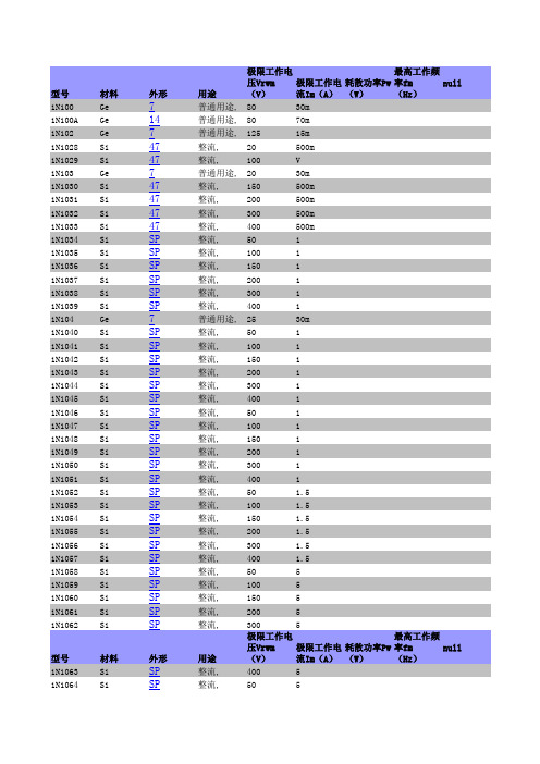
型号材料外形用途极限工作电压Vrwm(V)极限工作电流Im(A)耗散功率Pw(W)最高工作频率fm(H稳压)V稳压1N1313Si51稳压200μ150m8.75 1N1314Si51稳压200μ150m10.5 1N1315Si51稳压200μ150m12.71N1316Si51稳压200μ150m15.7 1N1317Si51稳压200μ150m18.5 1N1318Si51稳压200μ150m23.5 1N1319Si51稳压200μ150m28.5 1N1320Si51稳压200μ150m34.5 1N1321Si51稳压200μ150m41 1N1322Si51稳压200μ150m49.5 1N1323Si51稳压200μ150m58 1N1324Si51稳压200μ150m71 1N1325Si51稳压200μ150m87.5 1N1326Si51稳压200μ150m105 1N1327Si51稳压200μ150m127 1N1347Si SP整流,50061N1347A Si4整流,50061N1347B Si4整流,50061N1347C Si4整流,50061N1348Si SP整流,60061N1348A Si4整流,60061N1348B Si4整流,60061N1348C Si4整流,60061N135Ge7普通用途,755m1N1351Si4稳压500m10101N1351A Si4稳压500m1010 1N1351B Si SP稳压500m1010 1N1352Si4稳压500m10111N1352A Si4稳压500m1011 1N1352B Si SP稳压500m1011 1N1353Si4稳压500m1012 1N1353A Si4稳压500m1012 1N1353B Si稳压500m10121N1354Si4稳压500m10131N1354A Si4稳压500m1013 1N1354B Si SP稳压500m1013 1N1355Si4稳压500m10151N1355A Si4稳压500m1015 1N1355B Si SP稳压500m1015 1N1356Si4稳压500m1016 1N1356A Si4稳压500m1016 1N1356B Si SP稳压500m1016 1N1357Si4稳压500m1018 1N1357A Si4稳压500m1018 1N1357B Si SP稳压500m1018 1N1358Si4稳压150m1020 1N1358A Si4稳压150m1020 1N1358B Si SP稳压150m1020 1N1359Si4稳压150m1022 1N1359A Si4稳压150m1022 1N1359B Si SP稳压150m1022 1N1360Si4稳压150m1024 1N1360A Si4稳压150m1024 1N1360B Si SP稳压150m1024 1N1361Si4稳压150m1027 1N1361A Si4稳压150m1027 1N1361B Si SP稳压150m1027 1N1362Si4稳压150m1030 1N1362A Si4稳压150m1030 1N1362B Si SP稳压150m1030 1N1363Si4稳压150m1033 1N1363A Si4稳压150m1033 1N1363B Si SP稳压150m1033 1N1364Si4稳压150m1036 1N1364A Si4稳压150m1036 1N1364B Si SP稳压150m1036 1N1365Si4稳压150m1039 1N1365A Si4稳压150m1039 1N1365B Si SP稳压150m1039 1N1366Si4稳压150m1043 1N1366A Si4稳压150m1043 1N1366B Si SP稳压150m1043 1N1367Si4稳压150m1047 1N1367A Si4稳压150m1047 1N1367B Si SP稳压150m1047 1N1368Si4稳压150m1051 1N1368A Si4稳压150m1051 1N1368B Si稳压150m10511N1369Si4稳压150m1056 1N1369A Si4稳压150m1056 1N1369B Si SP稳压150m1056 1N1370Si4稳压50m1062 1N1370A Si4稳压50m1062 1N1370B Si SP稳压50m1062 1N1371Si4稳压50m1068 1N1371A Si4稳压50m1068 1N1371B Si SP稳压50m1068 1N1372Si4稳压50m1075 1N1372A Si4稳压50m1075 1N1372B Si SP稳压50m1075 1N1373Si4稳压50m1082 1N1373A Si4稳压50m1082 1N1373B Si SP稳压50m1082 1N1374Si4稳压50m1091 1N1374A Si4稳压50m1091 1N1374B Si SP稳压50m1091 1N1375Si4稳压50m10100 1N1375A Si4稳压50m10100 1N1376Si SP整流,502401N1377Si SP整流,1002401N1378Si SP整流,1502401N1379Si SP整流,2002401N137A Si51整流,3630m1N137B Si51整流,3675m1N1380Si SP整流,3002401N1381Si SP整流,4002401N1382Si SP整流,5002401N138A Si51整流,1850m1N138B Si51整流,189.0m1N139Ge7普通用途,4670m1N1396Si SP整流,5070 1N1397Si SP整流,10070 1N1398Si SP整流,15070 1N1399Si SP整流,200701N140Ge7普通用途,6085m1N1400Si整流,300701N1401Si SP整流,40070 1N1402Si SP整流,50070 1N1403Si SP整流,60070 1N1406Si45整流,600125m型号材料外形用途极限工作电压Vrwm(V)极限工作电流Im(A)耗散功率Pw(W)最高工作频率fm(Hz)Vz1N1911Si47整流,400 1.59页</< html>9a页</< html>12页。
4N33

6 PIN DIP PHOTODARLINGTON PHOTOCOUPLERTIL113, 4NXX, H11BX SeriesFeatures:• 4NXX series: 4N29, 4N30, 4N31, 4N32, 4N33• H11BX series: H11B1, H11B2, H11B3, H11B255• High isolation voltage between inputand output (Viso=5000 V rms )• Creepage distance >7.62 mm• Operating temperature up to +110°C• Compact small outline package• Pb free and RoHS compliant.• UL approved (No. E214129)• VDE approved (No. 132249)• SEMKO approved• NEMKO approved• DEMKO approved• FIMKO approved• CSA approvedDescriptionThe TIL113, 4NXX and H11BX series of devices each consist of an infrared emitting diode optically coupled to a photo darlington detector.They are packaged in a 6-pin DIP package and available in wide-lead spacing and SMD option. ApplicationsLow power logic circuitsTelecommunications equipmentPortable electronicsInterfacing coupling systems of different potentials and impedancesSchematicPin Configuration1. Anode2. Cathode3. No Connection4. Emitter5. Collector6. BaseAbsolute Maximum Ratings (Ta=25℃)Parameter Symbol Rating UnitInput Forward current I F60 mA Peak forward current (1us, pulse) I FP 1 AReverse voltage V R 6 VPower dissipationNo derating required up to Ta = 100°C P D120 mW3.8 mW/°COutputPower dissipationDerating factor (above Ta = 80°C) P C 150 mW 6.5 mW/°CCollector-Emitter voltage V CEO55 VCollector-Base voltage V CBO55 VEmitter-Collector voltage V ECO7 VEmitter-Base voltage V EBO7 V Total power dissipation P TOT200 mW Isolation voltage V ISO5000 Vrms Operating temperature T OPR-55~+100 °C Storage temperature T STG-55~+125 °C Soldering temperature *2T SOL260 °C Notes:*1 AC for 1 minute, R.H.= 40 ~ 60% R.H. In this test, pins 1, 2 & 3 are shorted together, and pins 4, 5 & 6 are shorted together. *2 For 10 secondsElectro-Optical Characteristics (Ta=25℃unless specified otherwise)InputParameter Symbol Min. Typ.* Max. Unit ConditionForward Voltage V F- 1.2 1.5 V I F= 10mAI F= 50mA for H11B3Reverse Current I R- - 10 µA V R= 6VInput capacitance C in- 50 - pF V = 0, f = 1MHz OutputParameter Symbol Min. Typ.* Max. Unit ConditionCollector-Emitter darkcurrentI CEO- - 100 nA V CE= 10V Collector-Emitterbreakdown voltageBV CEO55 - - V I c=1mAEmitter-Collectorbreakdown voltageBV CBO55 - - V I C=0.1mA Emitter-Collectorbreakdown voltageBV ECO7 - - V I E=0.1mATransfer Characteristics (Ta=25°C unless specified otherwise)Parameter Symbol Min Typ. Max. Unit ConditionCurrent transfer ratio4N324N33CTR500 - -%I F= 10mA ,V CE= 10V 4N294N30100 - -4N31 50 - -H11B1 500 - -I F= 1mA ,V CE= 5VH11B2 200 - -H11B3 100 - -H11B255 100 - - I F= 10mA ,V CE= 5V TIL113 300 - - I F= 10mA ,V CE= 1VTransfer Characteristics (T a=25°C unless specified otherwise)Parameter Symbol Min Typ. Max. Unit ConditionCollector-e mitter saturation voltage4N294N304N324N33V CE(sat)- - 1.0VI F = 8mA ,I c = 2mA4N31TIL113- - 1.2 I F = 8mA ,I c = 2mAH11B1H11B2H11B3- - 1.0 I F = 1mA ,I c = 1mAH11B255 - - 1.0 I F = 50mA ,I c = 50mAIsolation resistance R IO1011- - ΩV IO = 500Vdc Input-outputCapacitanceC IO- 0.8 - pF V IO = 0, f = 1MHzTurn-on timeH11B1H11B2H11B3H11B255Ton- 25 -µsV CC = 10V, I F = 10mA,R L = 100Ω4N294N304N314N324N33TIL113- - 5V CC = 10V, I C = 50mA,I F=200mATurn-off timeH11B1H11B2H11B3H11B255Toff- 18 -µsV CC = 10V,I F = 10mA,R L = 100Ω4N324N33TIL113- - 100 VCC= 10V,I C = 50mA,I F=200mA 4N294N304N31- - 40* Typical values at T a = 25°CTypical Electro-Optical Characteristics CurvesV CCI FOutputFigure 7. Switching Time Test Circuit & WaveformsOrder InformationPart Number4NXXY(Z)-Vor H11BXY(Z)-Vor TIL113Y(Z)-VNoteXX = Part No. for 4NX series (29, 30, 31, 32 or 33)X = Part No. for H11BX series (1, 2, 3 or 255)Y = Lead form option (S, S1, M or none)Z = Tape and reel option (TA, TB or none).V = VDE safety (optional)Option Description Packing quantity None Standard DIP-6 65 units per tube M Wide lead bend (0.4 inch spacing) 65 units per tube S (TA) Surface mount lead form + TA tape & reel option 1000 units per reel S (TB) Surface mount lead form + TB tape & reel option 1000 units per reel S1 (TA) Surface mount lead form (low profile) + TA tape & reel option 1000 units per reel S1 (TB) Surface mount lead form (low profile) + TB tape & reel option 1000 units per reelPackage Dimension (Dimensions in mm) Standard DIP TypeOption M TypeOption S TypeOption S1 TypeRecommended pad layout for surface mount leadformDevice MarkingNotesEL denotes Everlight4N33TIL113H11B1 denotes Part NumberY denotes 1 digit Year codeWW denotes 2 digit Week codeV denotes VDE safety (optional)EL4N33YWWVELH11B1YWWVELTIL113YWWV11DPC-0000021 Rev. 2Tape & Reel Packing SpecificationsTape dimensionsDimension No. A B Do D1 E F Dimension(mm) 10.4±0.1 7.5±0.1 1.5±0.1 1.5+0.1/-01.75±0.1 7.5±0.1 Dimension No. Po P1 P2 t W K Dimension(mm) 4.0±0.1512±0.12.0±0.10.35±0.0316.0±0.24.5±0.112Copyright © 2010, Everlight All Rights Reserved. Release Date : October 5, 2012. Issue No: DPC-0000021 Rev. 2Precautions for Use1. Soldering Condition1.1 (A) Maximum Body Case Temperature Profile for evaluation of Reflow ProfileNote: Reference: IPC/JEDEC J-STD-020DPreheatTemperature min (T smin ) 150 °C Temperature max (T smax )200°CTime (T smin to T smax ) (t s )60-120 seconds Average ramp-up rate (T smax to T p )3 °C/second maxOtherLiquidus Temperature (T L )217 °C Time above Liquidus Temperature (t L ) 60-100 sec Peak Temperature (T P )260°C Time within 5 °C of Actual Peak Temperature: T P - 5°C 30 sRamp- Down Rate from Peak Temperature 6°C /second max. Time 25°C to peak temperature 8 minutes max. Reflow times 3 times.DISCLAIMER1. Above specification may be changed without notice. EVERLIGHT will reserve authority on material change for abovespecification.2. When using this product, please observe the absolute maximum ratings and the instructions for using outlined in thesespecification sheets. EVERLIGHT assumes no responsibility for any damage resulting from use of the product which does not comply with the absolute maximum ratings and the instructions included in these specification sheets.3. These specification sheets include materials protected under copyright of EVERLIGHT corporation. Please don’treproduce or cause anyone to reproduce them without EVERLIGHT’s consent.13Rev. 。
维沙姆芯(Vishay Semiconductors)4N35、4N36、4N37三极管光导电阻说明

Document Number: 81181For technical questions, contact: *****************************Optocoupler, Phototransistor Output, with Base Connection4N35, 4N36, 4N37Vishay SemiconductorsDESCRIPTIONEach optocoupler consists of gallium arsenide infrared LED and a silicon NPN phototransistor.AGENCY APPROVALS•Underwriters laboratory file no. E52744•BSI: EN 60065:2002, EN 60950:2000•FIMKO; EN 60065, EN 60335, EN 60950 certificate no. 25156FEATURES•Isolation test voltage 5000 V RMS •Interfaces with common logic families •Input-output coupling capacitance < 0.5 pF •Industry standard dual-in-line 6 pin package •Compliant to RoHS directive 2002/95/EC and in accordance to WEEE 2002/96/ECAPPLICATIONS•AC mains detection •Reed relay driving•Switch mode power supply feedback •Telephone ring detection •Logic ground isolation•Logic coupling with high frequency noise rejection21842ORDER INFORMATIONPART REMARKS 4N35CTR > 100 %, DIP-64N36CTR > 100 %, DIP-64N37CTR > 100 %, DIP-6ABSOLUTE MAXIMUM RATINGS (1)PARAMETER TEST CONDITIONSYMBOLVALUEUNITINPUTReverse voltage V R 6V Forward current I F 50mA Surge current t ≤ 10 μsI FSM 1A Power dissipation P diss70mWOUTPUTCollector emitter breakdown voltage V CEO 70V Emitter base breakdown voltage V EBO 7V Collector current I C 50mA t ≤ 1 msI C 100mA Power dissipation P diss70mWCOUPLERIsolation test voltage V ISO5000V RMS Creepage ≥ 7mm Clearance≥ 7mm Isolation thickness between emitter and detector≥ 0.4mm For technical questions, contact: *****************************Document Number: 811814N35, 4N36, 4N37Vishay Semiconductors Optocoupler, Phototransistor Output,with Base ConnectionNotes (1)T amb = 25 °C, unless otherwise specified.Stresses in excess of the absolute maximum ratings can cause permanent damage to the device. Functional operation of the device is not implied at these or any other conditions in excess of those given in the operational sections of this document. Exposure to absolute maximum ratings for extended periods of the time can adversely affect reliability.(2)Refer to wave profile for soldering condditions for through hole devices (DIP).Notes (1)T amb = 25 °C, unless otherwise specified.Minimum and maximum values are testing requirements. Typical values are characteristics of the device and are the result of engineering evaluation. Typical values are for information only and are not part of the testing requirements.(2)Indicates JEDEC registered value.COUPLERComparative tracking index DIN IEC 112/VDE 0303, part 1175Isolation resistance V IO = 500 V, T amb = 25 °C R IO 1012ΩV IO = 500 V, T amb = 100 °CR IO 1011ΩStorage temperature T stg - 55 to + 150°C Operating temperature T amb - 55 to + 100°C Junction temperature T j 100°C Soldering temperature (2)max.10 s dip soldering: distance to seating plane≥ 1.5 mm T sld260°CELECTRICAL CHARACTERISTICS (1)PARAMETER TEST CONDITIONPARTSYMBOLMIN.TYP.MAX.UNITINPUTJunction capacitance V R = 0 V, f = 1 MHzC j 50pF Forward voltage (2)I F = 10 mAV F 1.3 1.5V I F = 10 mA, T amb = - 55 °CV F 0.91.3 1.7V Reverse current (2)V R = 6 V I R 0.110μA Capacitance V R = 0 V, f = 1 MHzC O25pFOUTPUTCollector emitter breakdown voltage (2)I C = 1 mA4N35BV CEO 30V 4N36BV CEO 30V 4N37BV CEO 30V Emitter collector breakdown voltage (2)I E = 100 μABV ECO7VOUTPUTCollector base breakdown voltage (2)I C = 100 μA, I B = 1 μA4N35BV CBO 70V 4N36BV CBO 70V 4N37BV CBO 70V Collector emitter leakage current (2)V CE = 10 V , I F = 04N35I CEO 550nA 4N36I CEO 550nA V CE = 10 V , I F = 04N37I CEO 550nA V CE = 30 V , I F = 0,T amb = 100 °C4N35I CEO 500μA 4N36I CEO 500μA 4N37I CEO 500μA Collector emitter capacitance V CE = 0C CE6pFCOUPLERResistance, input output (2)V IO = 500 V R IO 1011ΩCapacitance, input outputf = 1 MHzC IO0.6pFABSOLUTE MAXIMUM RATINGS (1)PARAMETER TEST CONDITIONSYMBOLVALUEUNIT4N35, 4N36, 4N37Optocoupler, Phototransistor Output,with Base ConnectionVishay SemiconductorsNote(1)Indicates JEDEC registered values.Note(1)Indicates JEDEC registered values.TYPICAL CHARACTERISTICST amb = 25 °C, unless otherwise speciedFig. 1 - Forward Voltage vs. Forward CurrentFig. 2 - Normalized Non-Saturated and Saturated CTR vs.LED Current Fig. 3 - Normalized Non-Saturated and Saturated CTR vs.LED CurrentFig. 4 - Normalized Non-Saturated and Saturated CTR vs.LED CurrentCURRENT TRANSFER RATIOPARAMETER TEST CONDITION PART SYMBOL MIN TYP.MAX UNITDC current transfer ratio (1)V CE = 10 V, I F = 10 mA4N35CTR DC100%4N36CTR DC100%4N37CTR DC100%V CE = 10 V, I F = 10 mA,T A = - 55 °C to + 100 °C4N35CTR DC4050%4N36CTR DC4050%4N37CTR DC4050%SWITCHING CHARACTERISTICSPARAMETER TEST CONDITION SYMBOL MIN.TYP.MAX.UNIT Switching time (1)V CC = 10 V, I C = 2 mA, R L = 100 Ωt on, t off10μsDocument Number: 81181For technical questions, contact: *****************************4N35, 4N36, 4N37Vishay Semiconductors Optocoupler, Phototransistor Output,with Base ConnectionFig. 5 - Normalized Non-Saturated and Saturated CTR vs.LED CurrentFig. 6 - Collector Emitter Current vs.Temperature and LED CurrentFig. 7 - Collector Emitter Leakage Current vs. Temperature Fig. 8 - Normalized CTR cb vs. LED Current and Temperature Fig. 9 - Normalized Photocurrent vs. I F and Temperature Fig. 10 - Normalized Non-Saturated h FE vs.Base Current and Temperature For technical questions, contact: *****************************Document Number: 811814N35, 4N36, 4N37 Optocoupler, Phototransistor Output,with Base ConnectionVishay SemiconductorsFig. 11 - Normalized h FE vs. Base Current and Temperature Fig. 12 - Propagation Delay vs. Collector Load ResistorFig. 13 - Switching Timing Fig. 14 - Switching SchematicDocument Number: 81181For technical questions, contact: *****************************4N35, 4N36, 4N37Vishay Semiconductors Optocoupler, Phototransistor Output,with Base ConnectionPACKAGE DIMENSIONS in millimetersPACKAGE MARKING For technical questions, contact: *****************************Document Number: 81181Legal Disclaimer Notice VishayDisclaimerALL PRODUCT, PRODUCT SPECIFICAT IONS AND DAT A ARE SUBJECT T O CHANGE WIT HOUT NOT ICE T O IMPROVE RELIABILITY, FUNCTION OR DESIGN OR OTHERWISE.Vishay Intertechnology, Inc., its affiliates, agents, and employees, and all persons acting on its or their behalf (collectively, “Vishay”), disclaim any and all liability for any errors, inaccuracies or incompleteness contained in any datasheet or in any other disclosure relating to any product.Vishay makes no warranty, representation or guarantee regarding the suitability of the products for any particular purpose or the continuing production of any product. To the maximum extent permitted by applicable law, Vishay disclaims (i) any and all liability arising out of the application or use of any product, (ii) any and all liability, including without limitation special, consequential or incidental damages, and (iii) any and all implied warranties, including warranties of fitness for particular purpose, non-infringement and merchantability.Statements regarding the suitability of products for certain types of applications are based on Vishay’s knowledge of typical requirements that are often placed on Vishay products in generic applications. Such statements are not binding statements about the suitability of products for a particular application. It is the customer’s responsibility to validate that a particular product with the properties described in the product specification is suitable for use in a particular application. Parameters provided in datasheets and / or specifications may vary in different applications and performance may vary over time. All operating parameters, including typical parameters, must be validated for each customer application by the customer’s technical experts. Product specifications do not expand or otherwise modify Vishay’s terms and conditions of purchase, including but not limited to the warranty expressed therein.Except as expressly indicated in writing, Vishay products are not designed for use in medical, life-saving, or life-sustaining applications or for any other application in which the failure of the Vishay product could result in personal injury or death. Customers using or selling Vishay products not expressly indicated for use in such applications do so at their own risk. Please contact authorized Vishay personnel to obtain written terms and conditions regarding products designed for such applications.No license, express or implied, by estoppel or otherwise, to any intellectual property rights is granted by this document or by any conduct of Vishay. Product names and markings noted herein may be trademarks of their respective owners. Revision: 13-Jun-161Document Number: 91000。
2SC3461中文资料(sanyo)中文数据手册「EasyDatasheet - 矽搜」
Ta=120°C
3
2
25°C
VCE=5V
10
--40°C
DC电7流增益,hFE
5
3 2
23
10 7 5
5 7 0.1 2 3 5 7 1.0 2 3 5 7 10
集电极电流,IC - 一个
ITR05612
VBE(星期六) - IC
IC / IB=5
3 2
基极 - 1发.0射极 Ta=--40°C 饱和电7 压,VBE(星期六) - V 25°C
5
3
2 23
120 °C
5 7 0.1 2 3 5 7 1.0
集电极电流,IC - 一个
2 3 5 7 10 ITR05614
No.1596–2/4
芯片中文手册,看全文,戳
2SC3461
IC -- VBE
9
VCE=5V
8
7
6 5 4
集电极电流,IC - 一个
3 2
2°0C Ta1=
三洋承担所造成产品使用AT超越,即使是瞬间值,设备故障不承担任何责任,额定数值(例如最大 额定值,工作环境范围或其他参数)任何产品规格及所有SANYO产品描述或此处包含上市.
芯片中文手册,看全文,戳
接上页.
Parameter
Gain-Bandwidth Product Output Capacitance Collector-to-Emitter Saturation Voltage Base-to-Emitter Saturation Voltage Collector-to-Base Breakdown Voltage Collector-to-Emitter Breakdown Voltage Emitter-to-Base Breakdown Voltage Collector-to-Emitter Sustain Voltage Turn-ON Time Storage Time Fall Time
4N33S中文资料

TRANSFER CHARACTERISTICS
AC Characteristic Turn-on Time(3) (4N32, 4N33) (4N29, 4N30, 4N31) Bandwidth(4,5) Turn-off Time(3) Test Conditions (IF = 200 mA, IC = 50 mA, VCC = 10 V) (Fig.7) Symbol ton toff BW 30 Min Typ Max 5.0 100 40 KHz µs Units
IF - LED INPUT CURRENT (mA)
TA - AMBIENT TEMPERATURE (˚C)
Fig. 3 Collector Current vs. Collector-Emitter Voltage
NORMALIZED TO: IF = 1 mA VCE = 5 V
Fig. 4 Dark Current vs. Ambient Temperature
0 0 1 2 3 4 5 6 7 8 9 10
0.01
0
20
40
60
80
100
ቤተ መጻሕፍቲ ባይዱ
VCE- COLLECTOR -EMITTER VOLTAGE (V)
TA - AMBIENT TEMPERATURE (˚C)
Fig. 5 Turn-On Time vs. Input Current
1000 RL = 1 k1 VCC = 10 V 100 1000
元器件交易网
GENERAL PURPOSE 6-PIN PHOTODARLINGTON OPTOCOUPLERS
DESCRIPTION
The 4N29, 4N30, 4N31, 4N32, 4N33 have a gallium arsenide infrared emitter optically coupled to a silicon planar photodarlington.
- 1、下载文档前请自行甄别文档内容的完整性,平台不提供额外的编辑、内容补充、找答案等附加服务。
- 2、"仅部分预览"的文档,不可在线预览部分如存在完整性等问题,可反馈申请退款(可完整预览的文档不适用该条件!)。
- 3、如文档侵犯您的权益,请联系客服反馈,我们会尽快为您处理(人工客服工作时间:9:00-18:30)。
4/25/00
200038B
元器件交易网
GENERAL PURPOSE 6-PIN PHOTODARLINGTON OPTOCOUPLERS
4N29
ELECTRICAL CHARACTERISTICS
4N30
4N31
4N32
4N33
(TA = 25°C Unless otherwise specified.)
IF - LED INPUT CURRENT (mA)
IF - LED INPUT CURRENT (mA)
4/25/00
200038B
元器件交易网
GENERAL PURPOSE 6-PIN PHOTODARLINGTON OPTOCOUPLERS
4N29 4N30 4N31 4N32 4N33
INPUT PULSE
OUTPUT
OUTPUT PULSE
Fig. 7 Switching Time Test Circuit and Waveforms
Notes * Indicates JEDEC registered data. 1. The current transfer ratio(IC/IF) is the ratio of the detector collector current to the LED input current with VCE @ 10 V. 2. Pulse test: pulse width = 300µs, duty cycle 62.0% . 3. For test circuit setup and waveforms, refer to figure 7.. 4. IF adjusted to IC = 2.0 mA and IC = 0.7 mA rms. 5. The frequency at which IC is 3dB down from the 1 KHz value. 6. For this test, LED pins 1 and 2 are common, and phototransistor pins 4,5 and 6 are common.
SCHEMATIC
ANODE 1
6 BASE
APPLICATIONS
• • • • • Low power logic circuits Telecommunications equipment Portable electronics Solid state relays Interfacing coupling systems of different potentials and impedances.
TRANSFER CHARACTERISTICS
DC Characteristic *Collector Output Current(1,2) (4N32, 4N33) (4N29, 4N30) (IF = 10 mA, VCE = 10 V, IB = 0) IC (CTR) (4N31) *Saturation Voltage(2) (4N29, 4N30, 4N32, 4N33) (4N31) (IF = 8.0 mA, IC = 2.0 mA) VCE(sat) Test Conditions Symbol Min 50 (500) 10 (100) 5 (50) 1.0 1.2 V mA (%) Typ Max Units
TYPICAL ELECTRO-OPTICAL CHARACTERISTIC CURVES
(25°C Free air temperature unless otherwise specified) (Cont.)
Test Circuit
Waveforms
VCC = 10 V I C = 50 mA INPUT RL I F = 200 mA INPUT PULSE WIDTH <1 ms ton 10% 90% tr toff tf
4N30
4N31
4N32
4N33
Fig. 2 Current Transfer Ratio vs. Ambient Temperature
CTR - CURRENT TRANSFER RATIO (NORMALIZED)
10
TA = 0˚C, 25˚C TA = 70˚C TA = 100˚C TA = -55˚C 1
ISOLATION CHARACTERISTICS
Characteristic Input-Output Isolation Voltage(6) (4N29, 4N30, 4N31, 4N32, 4N33) *(4N32) *(4N33) Isolation Resistance(6) Isolation Capacitance(6) Test Conditions (II-O 61 µA, Vrms, t = 1 min.) VDC VDC (VI-O = 500 VDC) (VI-O = , f = 1 MHz) RISO CISO VISO Symbol Min 5300 2500 1500 1011 0.8 Typ Max Units Vac(rms) V 1 pf
INDIVIDUAL COMPONENT CHARACTERISTICS
Parameter EMITTER *Input Forward Voltage *Reverse Leakage Current *Capacitance DETECTOR V *Collector-Emitter Breakdown Voltage *Collector-Base Breakdown Voltage *Emitter-Collector Breakdown Voltage *Collector-Emitter Dark Current DC Current Gain Test Conditions (IF = 10 mA) (VR = 3.0 V) (VF = 0 V, f = 1.0 MHz) (IC = 100 µA, IB = 0) (IC = 100 µA, IE = 0) (IE = 100 µA, IB = 0) (VCE = 10 V, Base Open) (VCE = 5.0 V, IC = 500 µA) Symbol VF IR C BVCEO BVCBO BVECO ICEO hFE 30 30 5.0 Min Typ 1.2 0.001 150 60 100 8 1 5000 100 V V nA Max 1.5 100 Unit V µA pF
CATHODE 2 5 COLLECTOR N/C 3 4 EMITTER
ABSOLUTE MAXIMUM RATINGS
Parameter TOTAL DEVICE Storage Temperature Operating Temperature Lead Solder Temperature Total Device Power Dissipation @ TA = 25°C Derate above 25°C EMITTER Continuous Forward Current Reverse Voltage
TRANSFER CHARACTERISTICS
AC Characteristic Turn-on Time(3) (4N32, 4N33) (4N29, 4N30, 4N31) Bandwidth(4,5) Turn-off Time(3) Test Conditions (IF = 200 mA, IC = 50 mA, VCC = 10 V) (Fig.7) Symbol ton toff BW 30 Min Typ Max 5.0 100 40 KHz µs Units
ICEO - COLLECTOR-EMITTER DARK CURRENT (nA)
10000 VCE = 10 V 1000
16
IC - COLLECTOR CURRENT (NORMALIZED)
14
12
IF = 10 mA
10 IF = 5 mA
100
8
10
6
1
4
IF = 2 mA
2
0.1
IF = 1 mA
0 0 1 2 3 4 5 6 7 8 9 10
0.01
0
20
40
60
80
100
VCE- COLLECTOR -EMITTER VOLTAGE (V)
TA - AMBIENT TEMPERATURE (˚C)
Fig. 5 Turn-On Time vs. Input Current
1000 RL = 1 k1 VCC = 10 V 100 1000
IF - LED INPUT CURRENT (mA)
TA - AMBIENT TEMPERATURE (˚C)
Fig. 3 Collector Current vs. Collector-Emitter Voltage
NORMALIZED TO: IF = 1 mA VCE = 5 V
Fig. 4 Dark Current vs. Ambient Temperature
4N29
4N30
4N31
4N32
4N33
FEATURES
• High sensitivity to low input drive current • Meets or exceeds all JEDEC Registered Specifications • VDE 0884 approval available as a test option -add option .300. (e.g., 4N29.300)
元器件交易网
GENERAL PURPOSE 6-PIN PHOTODARLINGTON OPTOCOUPLERS