3-D broadband ground-based polarimetric SAR data processing for the monitoring
基于超表面的超宽带隐身天线罩的仿真设计

现代电子技术Modern Electronics Technique2023年12月1日第46卷第23期Dec. 2023Vol. 46 No. 230 引 言频率选择表面(Frequency Selective Surface, FSS )是一种由周期性排列的金属片或任意几何形状的孔径元件组成的周期结构[1⁃2],因其具有独特的频率选择特性而引起研究者们的广泛关注,它广泛应用于空间滤波器[3]、偏振器[4]、隐身天线罩[5⁃6]。
在隐身领域,由于天线通常是强散射源,因此降低整个天线系统的雷达横截面(Radar Scattering Section, RCS )至关重要。
当外部电磁波照射天线系统时,将天线工作波段外的电磁信号反射到某些方向,缩减了天线的单站RCS 。
同时,FSS 天线罩对天线工作频率范围内的信号具有全传输特性,保证了工作频段内天线的正常通信。
然而,这种反射带外电磁波的方法仅适用于单站雷达,对于双站或多站雷达而言并没有较好的隐身效果。
近年来形成了一种结合FSS 和吸波器的设计思路,它被称为频率选择性吸波体(FSA )。
FSA 通常能够吸收带外的入射电磁波,并且由一个传输波段来传输通信信号。
FSA 的概念首先在文献[5]中被提到,它一般由两层结构组成,即上层的吸波结构和下层的FSS 结构。
上层的吸波结构通常由金属结构和损耗元件构成,下层的FSS 由孔径元件组成。
根据吸波波段与传输波段位置基于超表面的超宽带隐身天线罩的仿真设计熊 杰, 杨宝平(黄冈师范学院 物理与电信学院, 湖北 黄冈 438000)摘 要: 为了减小飞行器的多基站雷达散射截面,增加天线系统的隐身功能,提出一种基于超表面的超宽带隐身天线罩模型,该模型具有低频吸收、高频传输的特性。
提出的天线罩由位于上层的吸波结构和位于下层的频率选择结构组成。
上层由两个π型金属结构与工型金属结构组合而成,中间通过电阻元件连接,下层由“X ”字型周期缝隙结构组成,每个周期结构中一个电阻层结构对应4个“X ”字型FSS 结构。
PZT的半导体特性
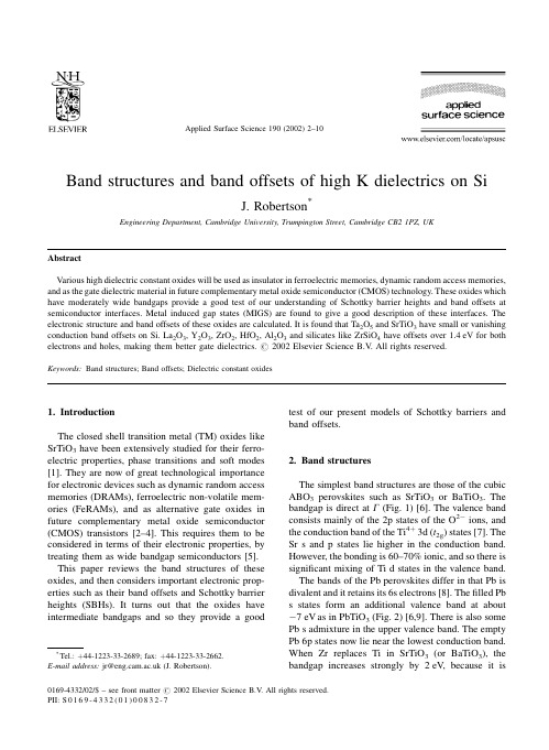
Band structures and band offsets of high K dielectrics on SiJ.Robertson *Engineering Department,Cambridge University,Trumpington Street,Cambridge CB21PZ,UKAbstractVarious high dielectric constant oxides will be used as insulator in ferroelectric memories,dynamic random access memories,and as the gate dielectric material in future complementary metal oxide semiconductor (CMOS)technology.These oxides which have moderately wide bandgaps provide a good test of our understanding of Schottky barrier heights and band offsets at semiconductor interfaces.Metal induced gap states (MIGS)are found to give a good description of these interfaces.The electronic structure and band offsets of these oxides are calculated.It is found that Ta 2O 5and SrTiO 3have small or vanishing conduction band offsets on 2O 3,Y 2O 3,ZrO 2,HfO 2,Al 2O 3and silicates like ZrSiO 4have offsets over 1.4eV for both electrons and holes,making them better gate dielectrics.#2002Elsevier Science B.V .All rights reserved.Keywords:Band structures;Band offsets;Dielectric constant oxides1.IntroductionThe closed shell transition metal (TM)oxides like SrTiO 3have been extensively studied for their ferro-electric properties,phase transitions and soft modes [1].They are now of great technological importance for electronic devices such as dynamic random access memories (DRAMs),ferroelectric non-volatile mem-ories (FeRAMs),and as alternative gate oxides in future complementary metal oxide semiconductor (CMOS)transistors [2±4].This requires them to be considered in terms of their electronic properties,by treating them as wide bandgap semiconductors [5].This paper reviews the band structures of these oxides,and then considers important electronic prop-erties such as their band offsets and Schottky barrier heights (SBHs).It turns out that the oxides have intermediate bandgaps and so they provide a goodtest of our present models of Schottky barriers and band offsets.2.Band structuresThe simplest band structures are those of the cubic ABO 3perovskites such as SrTiO 3or BaTiO 3.The bandgap is direct at G (Fig.1)[6].The valence band consists mainly of the 2p states of the O 2Àions,and the conduction band of the Ti 4 3d (t 2g )states [7].The Sr s and p states lie higher in the conduction band.However,the bonding is 60±70%ionic,and so there is signi®cant mixing of Ti d states in the valence band.The bands of the Pb perovskites differ in that Pb is divalent and it retains its 6s electrons [8].The ®lled Pb s states form an additional valence band at about À7eV as in PbTiO 3(Fig.2)[6,9].There is also some Pb s admixture in the upper valence band.The empty Pb 6p states now lie near the lowest conduction band.When Zr replaces Ti in SrTiO 3(or BaTiO 3),the bandgap increases strongly by 2eV,because itisApplied Surface Science 190(2002)2±10*Tel.: 44-1223-33-2689;fax: 44-1223-33-2662.E-mail address:jr@ (J.Robertson).0169-4332/02/$±see front matter #2002Elsevier Science B.V .All rights reserved.PII:S 0169-4332(01)00832-7controlled by the energy of the Zr d states.In contrast,in PZT,the Pb 6p states form the conduction band minimum,so the gap barely increases from 3.3to 3.7eV [10].It is recognised that the resonant covalence of Ti-d/O-p states is the origin of ferroelectricity in SrTiO 3type perovskites [11].In Pb perovskites,there is additional resonant covalence between Pb s and O p states which increases the ferroelectric polarity.SrBi 2Ta 2O 9is a layered crystal built from perovs-kite blocks separated by Bi 2O 2layers.It turns out that the Bi s and p states form the highest valence band and lowest conduction bands,respectively,while the ferro-electric response originates mainly from the TaO 3perovskite blocks [12].There is therefore an interest-ing separation of the functionality onto the Ta and Bi sub-lattices.Cubic ZrO 2has the ¯uorite structure.It has a simple band structure,as shown in Fig.3.The O p states form the valence band with a maximum at X [13].The conduction band minimum is at G ,and consists of Zr d states.The Zr d x 2Ày 2and d z 2states lie below the d xy states.The Zr s state lies midway between these at G ,but it disperses rapidly upwards.2.1.Models of Schottky barriers and semiconductor heterojunctionsThe band line-up of two semiconductors is deter-mined,like the SBH of a semiconductor on a metal,by charge transfer across the interface and the presence of any dipole layer at the interface.The charge transfer is that between the metal and the interface states of the semiconductor (Fig.4)[14].The charge transfertendsFig.1.Band structure of BaTiO 3calculated by pseudo-potential method [6].J.Robertson /Applied Surface Science 190(2002)2±103to align the Fermi level E F of the metal to the energy level of the interface states.The SBH for electrons f n between a semiconductor S and a metal M is f n S F M ÀF S F S Àw S(1)Here,F M is the work function of the metal,F S the energy of the semiconductor interface states,w S the semiconductor's electron af®nity (EA)and S the Schottky pinning parameter.S is given by [15]S11 e 2N d =ee 0(2)where e is the electronic charge,e 0the permittivity of free space,N the areal density of the interface states and d their decay length in the semiconductor.The dimensionless pinning factor S describes if the barrieris `pinned'or not.S varies between the limits S 1for unpinned Schottky barriers,and S 0for `Bardeen'barriers pinned by a high density of interface states in which the SBH is f n F S Àw S .There are numerous models of the origins of inter-face states,both intrinsic and extrinsic.In the intrinsic model originating from Bardeen and Heine,a semi-in®nite semiconductor in contact with a metal pos-sesses intrinsic states which are now called metal-induced gap states (MIGS)by Tersoff [14].F S is then the charge neutrality level (CNL)of the interface states,de®ned as the energy above which the states are empty for a neutral surface [16±18].On the other hand,the extrinsic models stress that the metal can react with the semiconductor [19].Brillson correlated the heat of reaction with S .This reaction maycreateFig.2.Band structure of PbTiO 3calculated by pseudo-potential method [6].4J.Robertson /Applied Surface Science 190(2002)2±10interface defects such as vacancies,whose gap states can pin the metal Fermi level,as noted by Spicer [20]and Dow [21].These models were supported by theobservation that pinning occurs even for monolayer coverage of metal,before the MIGS could be estab-lished.It is now believed that,overall,the intrinsic model gives a better description of Schottky barriers,because intrinsic states have a larger pinning dipole,N d ,than surface defects.The pinning parameter S has been in¯uential in our empirical understanding of Schottky barriers.Some years ago,Kurtin et al.[22]noted that S seemed to vary sharply with the ionicity of semi-conductor (Fig.5),from near 0for low ionicity semiconductors like Si and GaAs to 1for higher ionicity solids like SiO 2,SrTiO 3and KTaO 3.S is a dimensionless slope of barrier height to metal work function,S@f n @F M(3)Fig.3.Band structure of ZrO 2calculated by pseudo-potential method[6].Fig.4.Schematic diagram of SBHs.J.Robertson /Applied Surface Science 190(2002)2±105However,Louie [23]and Schluter [24]noted that Kurtin [22]had actually correlated the barrier heights to S H :S H@f n @X(4)which is the slope of barrier height to the Pauling electronegativity of the metal,and not the dimension-less S in (4).The work function and electronegativity vary roughly as [25,26]:F M 2:27X M 0:34(5)Thus,S H 2:27S ,and the Schottky limit should be S H 2:27.The data rarely reach this limit and Schluter [24]observed that S had a better correlation with the dielectric constant of the semiconductor e 0.Empiri-cally,Mo Ènch [14,27]found that S varied with e I as S11 0:1 e I À1 2(6)Certain materials are key tests of Schottky barriermodels.Diamond and xenon [14,28]have zero ioni-city but small e I ,and so their large S values show that S depends on e not on ionicity.This is tested by plotting log 1= S À1 against log e I À1 as in Fig.6.The wide gap oxides provide another key test,because they have intermediate e I values.SrTiO 3and KTaO 3were taken as high ionicity solids in the original Kurtin plot,with S H $1.However,this wasbefore data was actually known.When data [29]became available for SrTiO 3,showing S lying between 0.25and 0.4(Fig.6),it was clear that S is much lower.SrTiO 3falls well on the trend in Fig.3.The reason for this is that the SBHs depend on e I .e I is controlled by the states closest to the bandgap [5].In SrTiO 3,these are the moderately ionic Ti±O states of Ti±O bonds,not the highly ionic Sr±O states which lie well away from the gap and provide a much smaller contribution to e I .This can be seen in the partial density of states (DOS)of SrTiO 3in Fig.6.Thus,SrTiO 3and KTaO 3were misplaced in Fig.5as highly ionic solids.A lesser point is that the moderate value of S of SrTiO 3clearly correlates with e I ,and not with the low frequency dielectric constant e 0,which has a very large value for ferroelectrics and would give S %0from (6).SrTiO 3also serves as an evidence against the defect model,in that the barrier lies some way into the gap,not at the conduction band edge where the O vacancy states lie and would cause pinning.In sum-mary,the MIGS model of Schottky barriers holds for a wide range of solids of various ionicity and dielectric constants [5].The band alignment between two semiconductors is controlled by charge transfer and interface dipoles,just as Schottky barriers [30].For no dipoles,the Schottky limit,the conduction band offset isgivenFig.5.Schottky barrier pinning factor S H in the (incorrect)model of Kurtin etal.Fig. 6.Log±log plot of 1= S À1 vs.e I À1for various semiconductors and insulators to verify the MIGS model of Schottky barrier pinning factor S .6J.Robertson /Applied Surface Science 190(2002)2±10by the difference in their electron af®nities,the `elec-tron af®nity rule'.A similar idea was that for no charge transfer,the band line-ups are derived by placing each semiconductor's band on an absolute energy scale such as those of the free atom energy levels [31].Tersoff [16]showed that the band offset between two semiconductors a and b is controlled by interface dipoles as in the Schottky barrier,and so the conduc-tion band offset is given by f n w a ÀF CNL ;a À w b ÀF CNL ;bS F CNL ;a ÀF CNL ;b(7)The offsets are now described by aligning the CNLs of each semiconductor,modi®ed by the S factor.For simple semiconductors like Si,e I is large,and so S is small and the third term was negligible in the original formulation,but it is retained here for wide gap oxides.For strong pinning,the alignment is just given by the alignment of the two CNLs.The CNL energy below the vacuum level is a measure of the mean electronegativity of the semiconductor,in the same way that the work function of a metal is propor-tional to the metal's electronegativity.Thus,Eq.(7)says that the band alignment is the difference in electronegativity screened by the S factor.A wide ranging quantitative comparison found that the CNL models gives a good description of the band offsets [30].The CNL is the branch point of the semiconductor interface states.It is the integral of the Green's func-tion of the band structure,taken over the Brillouin zone [17],G E ZBZ N E H d H EE ÀE H0(8)Cardona and Christensen later provided a quicker method using a sum over special points of the Bril-louin zone [5,32].G E X i 1E ÀE i (9)2.2.Application to oxidesThe band alignments for the various wide gapoxides in contact with metal or silicon are found by calculating their CNLs and S parameters.The S factors are found from (6)using the experimental values of e Iand are shown in Table 1.The CNLs were found by calculating the oxide band structures by the tight-binding method [5,6,8,33].The tight-binding para-meters are found by ®tting to existing band structures [9,10,34],photoemission spectra and optical data [2,35±37].The CNLs for the various oxides are given in Table 1,together with the experimental values of their bandgaps and electron af®nities [2,38].SrTiO 3is an important oxide for future DRAM capacitor dielectrics.SrTiO 3is also the most studied system and the best test of our calculations.Fig.7compares the predicted SBHs of SrTiO 3on various metals with the experimental values [30,39±43].The experimental data are quite scattered but are quite consistent with S !1and our calculated value of 0.28.This shows that SrTiO 3is a key oxide in the tests of Schottky barrier models.The calculated barrier height for SrTiO 3on Pt is 0.9eV ,which is close to the 0.8eV found by photoemission by Copel et al.[43].However we cannot account for the much larger S value found by Shimizu et al.[42].BaTiO 3has similar band offsets to SrTiO 3.PbTi x Zr 1Àx O 3or PZT is an important ferroelectric for non-volatile memories,optical memories and other applications.The predicted barrier height for Pt onTable 1Calculated values for various oxides of their CNL and conduction band (CB)offset with Si aGap (eV)EA (eV)CNL (eV)e I S CB offset (eV)SiO 290.9 2.250.86 3.5b Si 3N 4 5.3 2.1 4.10.51 2.4b Ta 2O 5 4.4 3.3 3.3 4.840.40.3BaTiO 3 3.3 3.9 2.6 6.10.28À0.1BaZrO 3 5.3 2.6 3.740.530.8TiO 2 3.05 3.9 2.27.80.180.05ZrO 2 5.8 2.5 3.6 4.80.41 1.4HfO 26 2.5 3.740.53 1.5Al 2O 38.81c 5.5 3.40.63 2.8Y 2O 362c 2.4 4.40.46 2.3La 2O 36c 2c 2.440.53 2.3ZrSiO 46.5 2.4 3.6 3.80.56 1.5SrBi 2Ta 2O 94.13.53.35.30.4aExperimental values [36,37]of the bandgap,EA [2,38],dielectric constant e I [37]are also given.In Eqs.(2)and (5),F S is the energy of the CNL below the vacuum level,in this table,it is its energy above the valence band.bExperimental values.cEstimated values.J.Robertson /Applied Surface Science 190(2002)2±107PZT (Pb 0.55Zr 0.45O 3)is 1.45eV ,which is close to the 1.5eV measured by Dey et al.[44].The electron barrier of Pt on PZT is larger than that on BST because its CNL lies lower in the gap.This is because of the different band structure of PZT,in which the Pb 6s and 6p states form the band edges and this tends to lower the CNL.The larger value of the hole barrier than the electron barrier means that PZT thin ®lms can have predominantly electron injection,even though bulk PZT tends to be p-type.SrBi 2Ta 2O 9(SBT)is an important ferroelectric for non-volatile memories [2,45].It does not suffer from the loss of switchable polarisation (fatigue)when used with Pt electrodes,which is a problem for PZT.Note that more recent optical data ®nd that the bandgap of SBT is 4.1eV [2].The Schottky barrier of Pt is predicted to be 1.2eV ,which is essentially the same as that found by photoemission [46].There is an important need for high dielectric constant oxides to act as gate oxides instead of silicon dioxide [3,4].This is because the SiO 2layer is now so thin (2nm),that it no longer acts as a good insulator because of direct tunnelling across it.The solution is to replace SiO 2with a thicker layer of a medium k oxide,with the same equivalent capacitance or `equivalence oxide thickness't ox .The oxides must also satisfy certain other conditions,including chemi-cal stability in contact with Si [47].This rules out Ti and Ta which both react with Si to form SiO 2.The other key requirement is that they act as barriers toboth electrons and holes [5,32].This requires that both their valence and conduction band offsets be over 1eV .There is presently considerable effort to identify the most effective oxide,from a choice of ZrO 2,HfO 2,La 2O 3,Y 2O 3,Al 2O 3and the silicates ZrSiO 4and HfSiO 4.The calculated CB band offsets with Si are given in Table 1and summarised in Fig.8.They are compared in Table 2with recent experimental values [48±53],which is seen to be in good agreement.The important feature of Ta 2O 5and SrTiO 3is that both of them have CB offsets on Si under 1eV ,in fact 0in the case of SrTiO 3.This prediction was recently con®rmed by photoemission data of Chambers et al.[48].This means that SrTiO 3or BST cannot be a good gate oxide.The calculated CB offset for Ta 2O 5is only 0.36eV for Ta 2O 5on Si.This is consistent with recent photoemission data of Miyazaki and Hirose [49].Data for Ta 2O 5gate FETS also showed only a small elec-tron barrier [50].The CB offsets for BST and Ta 2O 5and BST are small or negligible because the bandgap is quite small and the band offsets are so asymmetric.To increasetheparison of calculated and observed SBHs of SrTiO 3on variousmetals.Fig.8.Predicted band offsets of various oxides on Si.Table 2Comparison of calculated and experimental values [48±53]of conduction band offsets on SiCalculatedExperiment References Ta 2O 50.350Miyazaki SrTiO 3À0.1<0.1Chambers ZrO 2 1.4 1.4Miyazaki 2.0Houssa Al 2O 32.82.8Ludeke8J.Robertson /Applied Surface Science 190(2002)2±10CB offset,we must either increase the bandgap or lower the CNL.The gap can be increased by raising the TM d levels,by using4d or5d metals instead of3d metals or using group IIIB metals instead of group IV. We should use zirconates,not titanates.The gap of BaZrO3is2eV wider than BaTiO3.Its offset is0.8eV.A better strategy is to lower the CNL.The CNL is lowered if the metal valence is lowered from4to3. Indeed,in Y2O3and La2O3,the CNL is much lower in the bandgap.Y2O3and La2O3are the oxides with largest CB offsets for reasonable dielectric constants. ZrO2has a bandgap of5.8eV,which is slightly wider than BaZrO3,and it also has a lower metal/ oxygen stoichiometry.This gives a larger CB offset for ZrO2(1.4eV)than BaZrO3,and indeed one which is just high enough.HfO2is similar.The calculated CB offset of1.4eV for ZrO2compares with an experi-mental value of1.4eV from photoemission[51]and a value of2eV by internal photoemission[52].This CB offset is large enough for devices.Zirconium silicate ZrSiO4and hafnium silicate HfSiO4are glassy oxides with bandgaps of $6.5eV.ZrSiO4consists of chains of alternate edge-sharing ZrO4and SiO2tetrahedra,with addi-tional Zr±O bonds between the chains,leading to an overall six-fold Zr coordination.We estimate the bandgap of ZrSiO4to be6.5eV.The calculated CB offsets are1.5eV,slightly more than ZrO2.Al2O3has a bandgap of8eV close to SiO2but with a higher k($9).Its calculated CB offset is2.8eV, which compares exactly with that measured by Ludeke et al.[53].Overall,the agreement between the calculated and subsequent experimental values for CB offsets in Table2is surprisingly good.References[1]M.E.Lines,X.Glass,Ferroelectrics,Oxford UniversityPress,Oxford,1990.[2]J.F.Scott,Ferroelectrics Rev.1(1998)1.[3]G.D.Wilk,R.M.Wallace,J.M.Anthony,J.Appl.Phys.89(2001)5243.[4]A.I.Kingon,J.P.Maria,S.K.Streiffer,Nature406(2000)1032.[5]J.Robertson,J.Vac.Sci.Technol.B18(2000)1785.[6]P.W.Peacock,J.Robertson,Unpublished work.[7]L.F.Mattheis,Phys.Rev.B6(1972)4718.[8]J.Robertson,W.L.Warren,B.A.Tuttle,D.Dimos,D.M.Smyth,Appl.Phys.Lett.63(1993)1519.[9]R.D.King-Smith,D.Vanderbilt,Phys.Rev.B49(1994)5828.[10]J.Robertson,W.L.Warren,B.A.Tuttle,J.Appl.Phys.77(1995)3975.[11]R.E.Cohen,Nature358(1992)136.[12]J.Robertson,C.W.Chen,W.L.Warren,C.D.Gutleben,Appl.Phys.Lett.69(1996)1704.[13]R.H.French,S.J.Glass,F.S.Ohuchi,Y.N.Xu,W.Y.Ching,Phys.Rev.B49(1994)5133.[14]W.MoÈnch,Phys.Rev.Lett.58(1987)1260.[15]W.MoÈnch,Surf.Sci.300(1994)928.[16]A.W.Cowley,S.M.Sze,J.Appl.Phys.36(1965)3212.[17]C.Tejedor,F.Flores,E.Louis,J.Phys.C10(1977)2163.[18]J.Tersoff,Phys.Rev.Lett.52(1984)465.[19]J.Tersoff,Phys.Rev.B30(1984)4874;J.Tersoff,Phys.Rev.B32(1985)6989.[20]L.J.Brillson,Surf.Sci.300(1994)909.[21]W.E.Spicer,T.Kendelewicz,N.Newman,K.K.Chin,I.Lindau,Surf.Sci.168(1986)240.[22]R.E.Allen,O.F.Sankey,J.D.Dow,Surf.Sci.168(1986)376.[23]S.Kurtin,T.C.McGill,C.A.Mead,Phys.Rev.Lett.30(1969)1433.[24]S.G.Louie,J.R.Chelikowsky,M.L.Cohen,Phys.Rev.B15(1977)2154.[25]M.Schluter,Phys.Rev.B17(1978)5044;M.Schluter,Thin Solid Films93(1982)3.[26]W.Gordy,W.J.O.Thomas,Phys.Rev.24(1956)439.[27]H.B.Michaelson,J.Appl.Phys.48(1977)4729.[28]W.MoÈnch,Phys.Rev.Lett.58(1986)1260.[29]W.MoÈnch,Europhys.Lett.27(1994)479.[30]R.C.Neville,C.A.Mead,J.Appl.Phys.43(1972)4657.[31]W.A.Harrison,J.Vac.Sci.Technol.14(1977)1016.[32]M.Cardona,N.E.Christensen,Phys.Rev.B35(1987)6182.[33]E.T.Yu,J.O.McCaldin,T.C.McGill,Solid State Phys.46(1992)1.[34]J.Robertson,C.W.Chen,Appl.Phys.Lett.74(1999)1168.[35]G.M.Rignanese,X.Gonze,A.Pasquarello,Phys.Rev.B63(2001)104305.[36]R.H.French,J.Am.Ceram.Soc.73(1990)477.[37]E.D.Palik,Handbook of Optical Properties of Solids,V ol.1±3,Academic Press,New York,1985.[38]W.Schmickler,J.W.Schultze,in:J.M.O'Bockris(Ed.),Modern Aspects of Electrochemistry,V ol.17,Plenum Press, London,1986.[39]G.W.Dietz,W.Antpohler,M.Klee,R.Waser,J.Appl.Phys.78(1995)6113.[40]H.Hasegawa,T.Nishino,J.Appl.Phys.69(1991)1501.[41]K.Abe,S.Komatsu,Jpn.J.Appl.Phys.31(1992)2985.[42]T.Shimizu,N.Gotoh,N.Shinozaki,H.Okushi,App.Surf.Sci.117(1997)400;()T.Shimizu,N.Gotoh,N.Shinozaki,H.Okushi,Mat.Res.Soc.Symp.Proc.(2000).[43]M.Copel,P.R.Duncombe,D.A.Neumayer,T.M.Shaw,R.M.Tromp,Appl.Phys.Lett.70(1997)3227.[44]S.K.Dey,J.J.Lee,P.Alluri,Jpn.J.Appl.Phys.34(1995)3134.[45]C.A.Paz de Araujo,J.D.Cuchiaro,L.D.McMillan,M.C.Scott,J.F.Scott,Nature374(1995)627.[46]C.D.Gutleben,Appl.Phys.Lett.71(1997)3444.[47]H.J.Hubbard,D.G.Schlom,J.Mater.Res.11(1996)2757.J.Robertson/Applied Surface Science190(2002)2±109[48]S.A.Chambers,Y.Liang,Z.Yu,R.Dropad,J.Ramdani,K.Eisenbeiser,Appl.Phys.Lett.77(2000)1662.[49]S.Miyazaki,Appl.Surface Science(2002)``these proceed-ings''.[50]S.Miyazaki,M.Narasaki,M.Ogasawara,M.Hirose,Microelec.Eng.59(2001)373.[51]A.Chatterjee,et al.,IEDM Tech Digest,1998,p.777.[52]M.Houssa,M.Tuominen,M.Nailli,V.Afansev, A.Stesmans,J.Appl.Phys.87(2000)8615.[53]R.Ludeke,M.T.Cuberes,E.Cartier,Appl.Phys.Lett.76(2000)2886;D.J.Maria,J.Appl.Phys.45(1974)5454.10J.Robertson/Applied Surface Science190(2002)2±10。
L波段宽调谐范围的取样光栅分布布拉格反射激光器设计

第41卷第10期2020年10月发光学报CHINESE JOURNAL OF LUMINESCENCEVol.41No.10Oct.,2020文章编号:1000-7032(2020)10-1279-08L 波段宽调谐范围的取样光栅分布布拉格反射激光器设计徐长达1,2,陈伟1*,班德超1,2,孙文惠1(1.中国科学院半导体研究所固态光电信息技术实验室,北京100083;2.中国科学院大学材料科学与光电技术学院,北京100049)摘要:L 波段取样光栅分布布拉格反射(SG-DBR)激光器在高速光通信与无源光网络中具有广泛的应用前景。
本文以InGaAsP 作为无源波导区材料,从理论上分析了实现L 波段宽调谐SG-DBR激光器所需的关键参数,包括前后取样光栅的反射峰间隔、取样周期、占空比等。
同时采用传输矩阵模型,讨论了取样对数与前、后取样光栅反射特性的关系。
最后得到了一组优化的SG-DBR激光器参数,其对应的调谐范围达到47.6nm 。
关键词:L 波段;传输矩阵法;SG-DBR激光器;宽调谐范围中图分类号:TN248.4文献标识码:ADOI :10.37188/CJL.20200201Design of Sampled Grating Distributed BraggReflector Laser with Wide Tuning Range in L-bandXU Chang-da 1,2,CHEN Wei 1*,BAN De-chao 1,2,SUN Wen-hui 1(1.Laboratory of Solid State Optoelectronic Information Technology ,Institute of Semiconductors ,Chinese Academy of Sciences ,Beijing 100083,China ;2.College of Materials Science and Opto-Electronic Technology ,University of Chinese Academy of Sciences ,Beijing 100049,China )*Corresponding Author ,E-mail :wchen @semi.ac.cnAbstract :L-band SG-DBRlasers have wide application prospects in high-speed optical communica-tion and passive optical networks.In this paper ,using InGaAsP as the passive waveguide region ma-terial ,the key parameters which are necessary to realize the wide-tuned SG-DBRlaser in L-band are theoretically analyzed ,including the reflection peak interval ,number of sample period and duty ratio of the sampled grating.At the same time ,the relationship between the sampling logarithm and the reflection characteristics of the front sampling grating (FSG )and rear sampling grating (RSG )is dis-cussed by using the transmission matrix model.Finally ,a set of optimized SG-DBRlaser parameters were obtained ,and the corresponding tuning range reached 47.6nm.Key words :L-band ;transmission matrix method ;SG-DBRlaser ;wide tuning range收稿日期:2020-07-11;修订日期:2020-08-10基金项目:国家重点研发计划;中国科学院青年创新促进会资助项目Supported by National Key R&D Program of China ;Youth Innovation Promotion Association of The Chinese Academy of Sci-ences1引言为了进一步提高通信容量,波分复用技术不断从C 波段延伸到L 波段,随着信道数的增加,固定波长激光器的备份压力也不断增大,而可调谐激光器通过覆盖相邻的信道波长,可以减少固定波长激光器的备份数量,被认为是波分复用光系统中的理想光源。
基于三维光谱指数的春小麦SPAD_高光谱估算

收稿日期:2022-02-15基金项目:伊犁师范大学博士科研启动基金项目(2020YSBSYJ001);伊犁师范大学大学生创新训练项目(X20201076406)作者简介:刘晓翠(1999-),女,甘肃武威人,本科,主要从事遥感数值建模研究,(电话)177****9554(电子信箱)*****************;通信作者,尼加提·卡斯木(1991-),男(维吾尔族),新疆伊宁人,副教授,博士,主要从事高光谱遥感数值建模研究,(电话)136****0391(电子信箱)******************。
刘晓翠,吾木提·艾山江,尼加提·卡斯木.基于三维光谱指数的春小麦SPAD 高光谱估算[J ].湖北农业科学,2023,62(9):151-157.小麦(Triticum aestivum L.)作为中国重要的粮食作物,而超过95%的产量来源于叶片的光合作用[1]。
叶绿素含量SPAD 作为农作物光合作用中重要的参数之一,对叶绿素含量起到监测作用,有利于衡量农作物地上部分叶片光合能力[2,3]。
快速、无损、准确地监测农作物长势对区域尺度水肥管理和估产具有重要的指导意义,也是发展智慧农业的需要。
随着遥感技术的迅速发展,尤其是高光谱遥感技术的不断提升,以其快速、无损和高效等优势在智慧和精准农业领域被广泛应用[4]。
目前,利用高光谱遥感技术对作物主要参数(地上生物量[5]、叶片氮磷含量[6]、LAI [7]、叶片水分[8]等)进行估算,已经体现出明显优势。
在农作物SPAD 的遥感监测中,高光谱遥感发挥重要的作用,Al-Abbas 等[9]、Hinzman基于三维光谱指数的春小麦SPAD 高光谱估算刘晓翠,吾木提·艾山江,尼加提·卡斯木(伊犁师范大学生物与地理科学学院/资源与生态研究所,新疆伊宁835000)摘要:为探讨三维光谱指数(TBI )对春小麦(Triticum aestivum L.)SPAD (Soil and plant analyzer development )估算的可行性,在田间尺度上以春小麦为目标,采集抽穗期冠层高光谱数据并计算任意波段组合的三维光谱指数,构建基于最优三维光谱指数的春小麦SPAD 估算模型。
宽波束天线技术综述
Science and Technology&Innovation I科技与创新|2021年第04期]---------------文章编号:2095-6835(2021)04-0161-03宽波束天线技术综述柯晨希1,李铭伟2(1.武汉理工大学,湖北武汉430070;2.空军预警学院,湖北武汉430019)摘要:概述了宽波束天线的研究现状,总结了宽波束天线的关键技术,介绍了宽带宽、低剖面宽波束天线。
并根据当前研究的热点问题,提出对宽波束天线未来研究方向的展望。
关键词:天线;宽波束;宽带宽;低剖面中图分类号:TN927文献标志码:A1引言天线作为无线通信系统中重要的射频前端组件,用于接收和辐射电磁波,实现电磁波与导行波的相互转换。
近年来,随着民用无线电通信系统,军用雷达、电子对抗等新型武器装备的研制成功,宽波束天线技术得到了进一步发展。
在卫星定位、雷达探测、电子对抗等无线电通信系统中,为了确保信号传输质量和传输速率,天线往往要具备很宽的波束宽度和较宽的频带[1]。
同时,随着现代无线电通信系统朝着小型化趋势发展,天线的低剖面设计也是当前的一个研究热点。
如何设计一款高性能的宽波束天线,是确保整个系统性能的关键。
本文总结了宽波束天线的发展现状,介绍了几种宽波速天线,并且根据当前研究的热点问题,提出对宽波束天线未来研究方向的展望。
2宽波束天线的研究现状传统的微带天线的3dB轴比波束宽度(ARBW)约为70。
~100。
在早期的无线通信系统中,传统的四臂螺旋天线就可以做到这点,这是因为其远场方向图波束宽度相对比较宽。
但由于地板的制约,传统的微带天线波束不可能展到很宽。
为满足实际运用需求,人们对波束展宽技术的研究一直在进行。
至此,许多学者提出了许多展宽天线的轴比波束宽度的方法。
虽然方式不同,算法各异,但技术思想一般都是在调整两个正交场分量的远场波束形状或波束宽度,在宽角度范围内保持它们的波束形状几乎相等闵。
星载高光谱成像系统发展综述
航天返回与遥感第44卷第6期12 SPACECRAFT RECOVERY & REMOTE SENSING2023年12月星载高光谱成像系统发展综述刘思田卢慧王栋李晓兰朱春丽边丽蘅*(北京理工大学复杂环境智能感测技术工信部重点实验室,北京100081)摘要高光谱遥感技术通过记录地表物体在多个连续波段下的光谱信息,实现高精度的地球观测与分析。
为了获取更多地物目标的细节信息,研究人员提出了对高光谱成像系统各项参数指标的新要求,国内外开展了大量相关研究。
随着卫星技术的成熟,高光谱遥感平台从最初的机载平台逐渐发展到星载平台,促进了高光谱遥感图像在地质、农林业、环境监测等领域的广泛应用。
目前,多数光谱成像系统选用传统的光学器件来实现分光,将计算光学与高光谱遥感结合,有利于集成更紧凑便捷的成像系统。
文章首先介绍了高光谱成像系统的主要类型和原理,随后对近30年来典型的星载高光谱成像系统及载荷进行了综述,梳理了典型国内外星载高光谱成像系统的发展现状,并对不同国家成像系统的性能指标进行了对比分析,总结了相应的发展历程,并对未来星载高光谱成像系统的发展作出了展望。
关键词高光谱成像系统遥感载荷星载光谱成像仪发展趋势中图分类号:V248.1;TP391.41文献标志码: A 文章编号: 1009-8518(2023)06-0012-15 DOI: 10.3969/j.issn.1009-8518.2023.06.002Overview of Development Analysis of Space-Borne HyperspectralImaging SystemLIU Sitian LU Hui WANG Dong LI Xiaolan ZHU Chunli BIAN Liheng*(MIIT Key Laboratory of Complex-Field Intelligent Sensing, Beijing Institute of Technology, Beijing 100081, China)Abstract Hyperspectral remote sensing technology provides high-precision earth observation and analysis by recording the spectral information of ground objects over multiple continuous wavelength bands. To obtain more detailed information about the earth’s surface, researchers worldwide have conducted extensive studies on various parameters of hyperspectral remote sensing payloads. With satellite technology maturing, hyperspectral remote sensing has shifted from airborne platforms to satellites, broadening applications in geology, agriculture, forestry, and environmental monitoring. Most spectral imaging systems now rely on traditional optical components for spectral separation. Combining computational optics with hyperspectral remote sensing is conducive to integrating more compact and convenient imaging systems. This paper initiates by introducing the principal types and principles of hyperspectral imaging instruments. It subsequently offers an overview of conventional space-borne hyperspectral remote sensing payloads spanning the last three decades. It analyses the present status of typical hyperspectral payloads on both domestic and international fronts, undertaking a comparative evaluation of their performance metrics. Finally, the paper concludes by encapsulating the associated trends in development. Furthermore, this paper offers insights into the future收稿日期:2023-09-25基金项目:国家自然科学基金面上项目(61971045);国家优秀青年科学基金项目(62322502)引用格式:刘思田, 卢慧, 王栋, 等. 星载高光谱成像系统发展综述[J]. 航天返回与遥感, 2023, 44(6): 12-26.LIU Sitian, LU Hui, WANG Dong, et al. Development Analysis of Spaceborne Hyperspectral Imaging System[J].Spacecraft Recovery & Remote Sensing, 2023, 44(6): 12-26. (in Chinese)第6期刘思田等: 星载高光谱成像系统发展综述 13trends of hyperspectral remote sensing payloads, providing valuable references for advancing research and applications of hyperspectral remote sensing payloads in China.Keywords hyperspectral imager; remote sensing payload; space-borne spectral imager; development trend0 引言高光谱遥感是一种基于成像光谱理论的遥感方法,旨在同时捕获地物的光谱信息和空间位置关系,以实现对地球表面的精确观测和深入分析。
喜马拉雅东构造结岩石圈板片深俯冲的地球物理证据
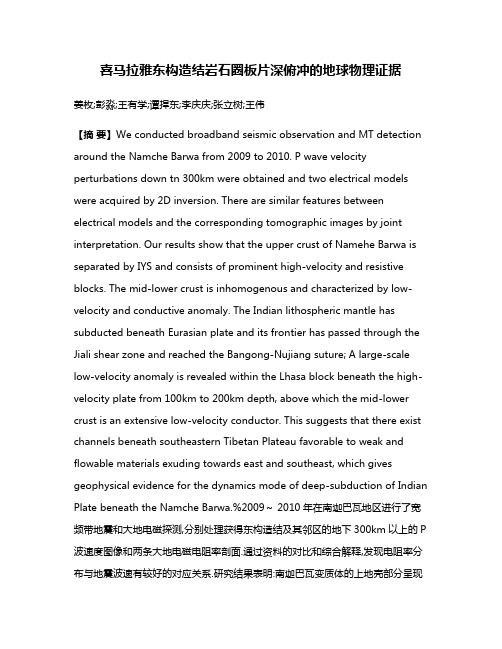
喜马拉雅东构造结岩石圈板片深俯冲的地球物理证据姜枚;彭淼;王有学;谭捍东;李庆庆;张立树;王伟【摘要】We conducted broadband seismic observation and MT detection around the Namche Barwa from 2009 to 2010. P wave velocity perturbations down tn 300km were obtained and two electrical models were acquired by 2D inversion. There are similar features between electrical models and the corresponding tomographic images by joint interpretation. Our results show that the upper crust of Namehe Barwa is separated by IYS and consists of prominent high-velocity and resistive blocks. The mid-lower crust is inhomogenous and characterized by low-velocity and conductive anomaly. The Indian lithospheric mantle has subducted beneath Eurasian plate and its frontier has passed through the Jiali shear zone and reached the Bangong-Nujiang suture; A large-scale low-velocity anomaly is revealed within the Lhasa block beneath the high-velocity plate from 100km to 200km depth, above which the mid-lower crust is an extensive low-velocity conductor. This suggests that there exist channels beneath southeastern Tibetan Plateau favorable to weak and flowable materials exuding towards east and southeast, which gives geophysical evidence for the dynamics mode of deep-subduction of Indian Plate beneath the Namche Barwa.%2009~ 2010年在南迦巴瓦地区进行了宽频带地震和大地电磁探测,分别处理获得东构造结及其邻区的地下300km以上的P 波速度图像和两条大地电磁电阻率剖面.通过资料的对比和综合解释,发现电阻率分布与地震波速有较好的对应关系.研究结果表明:南迦巴瓦变质体的上地壳部分呈现明显高速高阻特征,为两侧的雅鲁藏布江缝合带所夹持;中下地壳具有不均匀性,且普遍呈低速低阻特征;印度板块在藏东南向欧亚板块的俯冲前缘越过嘉黎断裂,抵达班公湖-怒江缝合带;在拉萨地体的高速俯冲板片以下100km至200km深度范围内存在大规模的低速异常带,其上盘中下地壳也广泛发育低速高导体,指示青藏高原东南缘可能存在韧性易流动的物质向东、东南逃逸的通道,为印度板块在南迦巴瓦的深俯冲动力学模式提供了地球物理证据.【期刊名称】《岩石学报》【年(卷),期】2012(000)006【总页数】10页(P1755-1764)【关键词】宽频地震;大地电磁;板片深俯冲;东构造结;喜马拉雅【作者】姜枚;彭淼;王有学;谭捍东;李庆庆;张立树;王伟【作者单位】中国地质科学院地质研究所,大陆构造与动力学国家重点实验室,北京100037;中国地质科学院地质研究所,大陆构造与动力学国家重点实验室,北京100037;中国地质大学地球物理与信息技术学院,北京100083;桂林理工大学地球科学学院,桂林541004;中国地质大学地球物理与信息技术学院,北京100083;中国地质科学院地质研究所,大陆构造与动力学国家重点实验室,北京100037;中国地质科学院地质研究所,大陆构造与动力学国家重点实验室,北京100037;中国地质科学院地质研究所,大陆构造与动力学国家重点实验室,北京100037;中国地质大学地球物理与信息技术学院,北京100083【正文语种】中文【中图分类】P313图1 喜马拉雅东构造结宽频地震台站及大地电磁测点位置IYS-雅鲁藏布江缝合带;JSZ-嘉黎剪切断裂带;BNS-班公湖-怒江缝合带;NJBW-南迦巴瓦东构造结;LS-拉萨地体;QT-羌塘地体;HM-喜马拉雅地体;INDB-印度陆块Fig.1 Map ofthe location of broadband seismic stations and magnetotelluric sites in Eastern Himalayan SyntaxisIYS-Indus-Yarlung Tsangpo suture; JSZ-Jiali shear zone; BNS-Bangong-Nujiang suture; NJBW-Namche Barwa tectonic syntaxis; LS-Lasa terrain; QT-Qiangtang terrain; HM-Himalaya terrain;INDB-Indian block印度板块与欧亚板块的碰撞一直以来都为广大地质、地球物理学家所关注,喜马拉雅造山带被公认为是印度板块与欧亚板块相碰撞的结果(Argand,1924;Yin and Harrison,2000;Tapponnier et al.,2001;许志琴等,2006a,b)。
advanced optical materials分区
Advanced Optical MaterialsIntroductionAdvanced optical materials refer to materials that possess uniqueoptical properties and have applications in various fields such as electronics, photonics, and optoelectronics. These materials are designed and engineered to manipulate light at the nanoscale, enabling the development of novel devices and technologies.Classification of Advanced Optical MaterialsAdvanced optical materials can be classified into several categories based on their properties and applications:1.Photonic Crystals: These materials have a periodic arrangement ofrefractive index variations, enabling the control and manipulation of light propagation. Photonic crystals find applications inoptical filters, waveguides, and sensors.2.Metamaterials: Metamaterials are artificially engineeredmaterials that possess unusual optical properties not found innaturally occurring materials. They have a unique refractive index and can exhibit negative refraction, enabling the development ofsuperlenses, invisibility cloaks, and other exotic devices.3.Plasmonic Materials: Plasmonic materials exhibit stronginteraction between light and free electrons at the nanoscale.They can confine and manipulate light beyond the diffraction limit, enabling the development of nanophotonic devices, biosensors, andenhanced solar cells.4.Quantum Dots: Quantum dots are semiconductor nanoparticles withunique optical properties. They can emit light of different colors depending on their size, making them useful in displays, lighting, and biological imaging.5.Nanophotonics: Nanophotonics involves the study and manipulationof light at the nanoscale. It combines nanotechnology, optics, and materials science to develop devices such as nanolasers, photoniccircuits, and ultra-sensitive detectors.6.Optical Fibers: Optical fibers are thin, flexible strands ofglass or plastic that can transmit light over long distances withminimal loss. They are used in telecommunications, medical imaging, and sensing applications.Applications of Advanced Optical MaterialsAdvanced optical materials have a wide range of applications across various fields:rmation Technology: Advanced optical materials are crucialfor the development of faster and more efficient data storage andcommunication technologies. Photonic crystals and metamaterialsare used in optical data storage, high-speed optical communication, and optical computing.2.Sensing and Imaging: Advanced optical materials play a vital rolein sensing and imaging technologies. Plasmonic materials andquantum dots are used in biosensors for detecting biologicalmolecules and in medical imaging for improved contrast andresolution.3.Energy: Advanced optical materials are used in solar cells toenhance light absorption and improve energy conversion efficiency.They are also used in light-emitting diodes (LEDs) for efficientand high-quality lighting.4.Optical Devices: Advanced optical materials enable thedevelopment of compact and efficient optical devices.Nanophotonics and photonic crystals are used in the fabrication of nanolasers, photonic integrated circuits, and ultra-sensitivedetectors.5.Biotechnology: Advanced optical materials have applications inbiotechnology and medicine. Quantum dots and plasmonic materialsare used for cellular imaging, drug delivery, and cancer therapy.Future OutlookThe field of advanced optical materials continues to evolve rapidly, driven by advancements in nanotechnology, materials science, and optics. Future research and development efforts are focused on:1.Enhancing Performance: Researchers are working on improving theoptical properties of advanced materials, such as increasing their efficiency, stability, and tunability.2.Integration and Miniaturization: The integration of advancedoptical materials into compact and multifunctional devices is amajor focus of ongoing research. This includes the development of on-chip photonic circuits and nanoscale optical devices.3.Biomedical Applications: Advanced optical materials hold greatpromise in biotechnology and medicine. Ongoing research aims todevelop targeted drug delivery systems, high-resolution imagingtechniques, and optical sensors for disease detection.4.Emerging Technologies: The field of advanced optical materials isalso exploring new technologies such as plasmonics, quantumphotonics, and 2D materials for novel applications incommunications, sensing, and computing.In conclusion, advanced optical materials offer immense potential for the development of next-generation devices and technologies. Their unique optical properties and versatile applications make them a vital area of research and innovation. Continued advancements in this field will drive progress in various sectors, from information technology to healthcare.。
- 1、下载文档前请自行甄别文档内容的完整性,平台不提供额外的编辑、内容补充、找答案等附加服务。
- 2、"仅部分预览"的文档,不可在线预览部分如存在完整性等问题,可反馈申请退款(可完整预览的文档不适用该条件!)。
- 3、如文档侵犯您的权益,请联系客服反馈,我们会尽快为您处理(人工客服工作时间:9:00-18:30)。
I.
INTRODUCTION
An important feature of electromagnetic wave scattering is its state of polarization, and a wide range of classification algorithms and inversion techniques have recently been developed based on the transformation of polarization state by scattering objects [1-3]. There are three primary ways in which multi-parameter radar measurements can be made: multifrequency, single or multi-baseline interferometry and multipolarization, and more recently a combination of these three approaches. Therefore, the combination of spatial information, spectral information and polarization information with multifrequency and broadband sensors defines the recent advances accomplished in polarimetric SAR systems development [4, 5]. GB-SAR is a new application of the conventional SAR expansion in the spatial domain. Based on derived GB-SAR principles and simulation results, we extended those earlier approaches and developed an ultra-wideband, ground-based, fully polarimetric SAR system
Wolfgang-Martin Boerner
ECE-CSN University of Illinois at Chicago Chicago, USA boerner@ for transverse and oblique vegetation monitoring [6]. The radar system consists of a vector network analyzer, a diagonal dual polarized broadband horn antenna an antenna positioning unit, and a PC-based control unit. We used the developed SAR system to carry out noninvasive measurements for three types of trees in three different seasons, namely in spring, summer and autumn, respectively. Three-dimensional (3-D) polarimetric images are reconstructed from the acquired data by a series of signal processing procedures based on a variety of wave front reconstruction methods. Combined signal processingarimetric SAR data and data interpretations for tree growth monitoring are addressed in this paper. II. FIELD EXPERIMENTS FOR TREE GROWTH MONITORING
A part of this work was supported by the Grant-In-Aid for Scientific Research (S)14102024 of JSPS.
Due to the fact that trees are some of the most important factors of the terrestrial vegetation cover, we selected an experimental site with different types of trees used for the noninvasive remote monitoring measurements. The main targets are denoted by T1, T2 and T3, and represented three different kinds of trees. T1 is a Japanese Zelkova, which is a deciduous tree that has no leaf in spring, exuberant broad leaves during early summer up to mid-autumn, after then leaves fallen off. T2 is a Japanese Cedar, which is an evergreen with needles. It almost does not change from spring to winter. T3 is a kind shrub of the Azalea genus which is a short bush surrounded by some plants: Japanese Honeysuckle. From spring to summer, they have very dense foliage while there are some stems and branches after autumn. We have carried out three measurements at the same exact position for the three different trees in late spring (April 19, 2002), in early summer (May 28, 2002) and in late autumn (November 11, 2002), respectively. There were a few fresh leaves during the first measurement in spring. Very significant growth in leaves and branches was observed in the second measurement in summer, while the third measurement was at a time when the leaves had fallen off. These measurement scenes are shown in Fig. 1 (on page 3 of this paper). HH, VH and VV polarization frequency domain data were acquired which cover frequency range from 1 GHz to 5 GHz.
Center for Northeast Asian Studies Tohoku University Sendai, Japan {zszhou, hamasaki, sato}@cneas.tohoku.ac.jp
Abstract—SAR is usually used for airborne or space borne remote sensing. It can also advantageously be exploited in a ground-based radar imaging system named Ground-based SAR (GB-SAR). We extended earlier approaches and developed an ultra-wideband, ground-based, fully polarimetric SAR (Pol-GBSAR) system for the monitoring of vegetation growth variations. Measurements on three type trees in different conditions were carried out by the developed SAR system. We proposed effective three-dimensional (3-D) broadband Pol-GB-SAR data processing algorithms in the paper. In situ polarimetric calibration obviously improved the features of the system. 3-D images were reconstructed from the acquired data by a series of signal processing procedures based on a variety of wave equation migration methods. By implementing methods of radar polarimetry, the broadband GB-SAR system has possibility for monitoring changes in tree structure characteristics due to seasonal variations. Interpreted results demonstrated the target scattering characteristics in different vegetation growth situations showed good agreement with the ground truth. Keywords-Ground-based SAR (GB-SAR); Radar Polarimetry; Polarimetric Calibration; 3-D Imaging Algorithms; Short Time Fourier Transform (STFT); Scattering Matrix; Vegetation Variation Identification