DM74LS241
关于74HC244芯片的中文资料

电源电压Vcc 54 4.5 5 5.5 V
74 4.75 5 5.25
输入高电平电ViH 2 V
输入低电平电ViL 54 0.7 V
74 0.8
输出高电平电流IOH 54 -12 mA
74 -15
输出低电平电流IOL 54 12 mA
74 24
求关于74HC244线接收器(3S,两组控制)
简要说明:
244为三态输出的八组缓冲器和总线驱动器,其主要电器特性的典型值如下(不同厂家具体值有差别):
型号 tPLH tphl PD
54LS241/74LS241 12ns 12ns 110mW
引出端符号:
1A1~1A4,2A1~2A4 输入端
/1G, /2G 三态允许端(低电平有效)
1Y1~1Y4,2Y1~2Y4 输出端
逻辑图:
双列直插封装
极限值:
电源电压 …………………………………………. 7V
输入电压 …………………………………………. 5.5V
tPHZ输出由高到高阻态禁止时间 Vcc=5V CL=5pF
RL=90 Ω 18 ns
tPLZ输出由低到高阻态禁止时间 25 ns
静态特性(TA为工作环境温度范围)
参 数 测 试 条 件【1】 LS244 单位
最小 最大
VIK输入嵌位电压 Vcc=最小,Iik=-18mA -1.5 V
输出高阻态时高电平电压 …………………………. 5.5V
工作环境温度
54XXX …………………………………. -55~125℃
74XXX …………………………………. 0~70℃
微机原理上机实验期末复习练习题

1.用74LS244设计一个输入接口。
从输入端口读入开关状态(高表示‘1’,低表示‘0’),以十进制形式在CRT显示器上显示输入结果(0~255)。
(244,43)如:输入开关状态:高高高高低低低低→CRT显示:2402.用74LS244和74LS273设计一个输入/输出接口,从输入端口输入原码数,转换为补码后从输出端口输出(高和亮表示‘1’,低和灭表示‘0’)。
(32,244,273)如:输入开关状态:低高高低低高低高→灭亮亮灭灭亮灭亮输入开关状态:高低低低低高低高→亮亮亮亮亮灭亮亮3.用AD0809设计一个A/D接口,从5VIN输入直流电压值,在CRT显示器上以二进制形式显示采样结果。
(0809,02)如:输入5V→CRT显示:1111 1111 B (允许有误差)如:输入0V→CRT显示:0000 0000 B4.用AD0809设计一个A/D接口,从5VIN输入直流电压值,在CRT显示器上以十进制形式显示采样结果。
(0809,02)如:输入5V→CRT显示:255( 允许有误差)如:输入0V→CRT显示:05.用AD0809设计一个A/D接口,从5VIN输入直流电压值,在CRT显示器上以0~FFFH的形式显示采样结果。
(0809,02)如:输入5V→CRT显示:FFH( 允许有误差)如:输入0V→CRT显示:00H6.用DAC0832设计一个D/A接口(单缓冲方式) 产生三角波, 端口地址仅为D883H。
(0832,138)7.用8255设计一个输入/输出接口,C口输入原码数,转换为补码后从B口输出(高和亮表示‘1’,低和灭表示‘0’)。
(8255)如:输入开关状态:低高高低低高低高→发光二极管: 灭亮亮灭灭亮灭亮输入开关状态:高低低低低高低高→发光二极管: 亮亮亮亮亮灭亮亮8.用8255设计一个输出接口,端口地址仅为D861H,从键盘输入两位十六进制数(00H~FFH),在发光二极管上以二进制形式显示其值(亮表示‘1’,灭表示‘0’)。
DM74LS240中文资料

© 2000 Fairchild Semiconductor Corporation DS006411August 1986Revised March 2000DM74LS240 • DM74LS241 Octal 3-STATE Buffer/Line Driver/Line ReceiverDM74LS240 • DM74LS241Octal 3-STATE Buffer/Line Driver/Line ReceiverGeneral DescriptionThese buffers/line drivers are designed to improve both the performance and PC board density of 3-STATE buffers/drivers employed as memory-address drivers, clock driv-ers, and bus-oriented transmitters/receivers. Featuring 400mV of hysteresis at each low current PNP data line input, they provide improved noise rejection and high fanout outputs and can be used to drive terminated lines down to 133Ω.Featuress 3-STATE outputs drive bus lines directly s PNP inputs reduce DC loading on bus lines s Hysteresis at data inputs improves noise margins s Typical I OL (sink current)24 mAs Typical I OH (source current)−15 mAs Typical propagation delay timesInverting 10.5 ns Noninverting12 nss Typical enable/disable time 18 ns s Typical power dissipation (enabled)Inverting 130 mW Noninverting135 mWOrdering Code:Devices also available in T ape and Reel. Specify by appending the suffix letter “X” to the ordering code.Connection DiagramsDM74LS240DM74LS241Order Number Package NumberPackage DescriptionDM74LS240WM M20B 20-Lead Small Outline Integrated Circuit (SOIC), JEDEC MS-013, 0.300 Wide DM74LS240SJ M20D 20-Lead Small Outline Package (SOP), EIAJ TYPE II, 5.3mm Wide DM74LS240N N20A 20-Lead Plastic Dual-In-Line Package (PDIP), JEDEC MS-001, 0.300 Wide DM74LS241WM M20B 20-Lead Small Outline Integrated Circuit (SOIC), JEDEC MS-013, 0.300 Wide DM74LS241NN20A20-Lead Plastic Dual-In-Line Package (PDIP), JEDEC MS-001, 0.300 Wide 2D M 74L S 240 • D M 74L S 241Function TablesDM74LS240DM74LS241L = LOW Logic Level H = HIGH Logic LevelX = Either LOW or HIGH Logic Level Z = High ImpedanceInputsOutput G A Y L L H L H L HXZInputs Outputs G G 1A 2A 1Y 2YX L L X L X L H X H X H X X ZH X X L L H X X H H LXXXZDM74LS240 • DM74LS241Absolute Maximum Ratings (Note 1)Note 1: The “Absolute Maximum Ratings” are those values beyond which the safety of the device cannot be guaranteed. The device should not be operated at these limits. The parametric values defined in the Electrical Characteristics tables are not guaranteed at the absolute maximum ratings.The “Recommended Operating Conditions” table will define the conditions for actual device operation.Recommended Operating ConditionsElectrical Characteristicsover recommended operating free air temperature range (unless otherwise noted)Note 2: All typicals are at V CC = 5V, T A = 25°C.Note 3: Not more than one output should be shorted at a time, and the duration should not exceed one second.Supply Voltage 7V Input Voltage7VOperating Free Air Temperature Range 0°C to +70°C Storage Temperature Range−65°C to +150°CSymbol ParameterMin Nom Max Units V CC Supply Voltage4.7555.25V V IH HIGH Level Input Voltage 2V V IL LOW Level Input Voltage 0.8V I OH HIGH Level Output Current −15mA I OL LOW Level Output Current 24mA T AFree Air Operating Temperature70°CSymbol ParameterConditions MinTyp Max Units (Note 2)V I Input Clamp Voltage V CC = Min, I I = −18 mA −1.5V HYS Hysteresis (V T + − V T −)V CC = Min0.20.4VData Inputs OnlyV OHHIGH Level Output VoltageV CC = Min, V IH = Min 2.7V IL = Max, I OH = −1 mA V CC = Min, V IH = Min 2.4 3.4VV IL = Max, I OH = −3 mA V CC = Min, V IH = Min 2V IL = 0.5V, I OH = MaxV OLLOW Level Output VoltageV CC = Min I OL = 12 mA 0.4V IL = Max I OL = Max 0.5VV IH = MinI OZH Off-State Output Current,V CC = Max V O = 2.7V 20µA HIGH Level Voltage Applied V IL = Max I OZL Off-State Output Current,V IH = MinV O = 0.4V−20µA LOW Level Voltage Applied I I Input Current at Maximum V CC = Max 0.1mA Input VoltageV I = 7VI IH HIGH Level Input Current V CC = Max, V I = 2.7V 20µA I IL LOW Level Input Current V CC = Max, V I = 0.4V −0.2mA I OS Short Circuit Output Current V CC = Max (Note 3)−40−225mAI CCSupply CurrentV CC = Max,Outputs HIGH 1323Outputs OPENOutputs LOW 26442746mA Outputs Disabled29503254 4D M 74L S 240 • D M 74L S 241Switching Characteristicsat V CC = 5V and T A = 25°C Symbol ParameterConditionsMax Units t PLH Propagation Delay Time C L = 45 pF DM74LS24014ns LOW-to-HIGH Level Output R L = 667ΩDM74LS24118t PHL Propagation Delay Time C L = 45 pF DM74LS24018ns HIGH-to-LOW Level Output R L = 667ΩDM74LS24118t PZL Output Enable Time C L = 45 pF DM74LS24030ns to LOW Level R L = 667ΩDM74LS24130t PZH Output Enable Time C L = 45 pF DM74LS24023ns to HIGH Level R L = 667ΩDM74LS24123t PLZ Output Disable Time C L = 5 pF DM74LS24025ns from LOW Level R L = 667ΩDM74LS24125t PHZ Output Disable Time C L = 5 pF DM74LS24018ns from HIGH Level R L = 667ΩDM74LS24118t PLH Propagation Delay Time C L = 150 pF DM74LS24018ns LOW-to-HIGH Level Output R L = 667ΩDM74LS24121t PHL Propagation Delay Time C L = 150 pF DM74LS24022ns HIGH-to-LOW Level Output R L = 667ΩDM74LS24122t PZL Output Enable Time C L = 150 pF DM74LS24033ns to LOW Level R L = 667ΩDM74LS24133t PZHOutput Enable Time C L = 150 pF DM74LS24026nsto HIGH LevelR L = 667ΩDM74LS24126 DM74LS240 • DM74LS241Physical Dimensions inches (millimeters) unless otherwise noted20-Lead Small Outline Integrated Circuit (SOIC), JEDEC MS-013, 0.300 WidePackage Number M20B 6D M 74L S 240 • D M 74L S 241Physical Dimensionsinches (millimeters) unless otherwise noted (Continued)20-Lead Small Outline Package (SOP), EIAJ TYPE II, 5.3mm WidePackage Description M20D7DM74LS240 • DM74LS241 Octal 3-STATE Buffer/Line Driver/Line ReceiverPhysical Dimensions inches (millimeters) unless otherwise noted (Continued)20-Lead Plastic Dual-In-Line Package (PDIP), JEDEC MS-001, 0.300 WidePackage Number N20AFairchild does not assume any responsibility for use of any circuitry described, no circuit patent licenses are implied and Fairchild reserves the right at any time without notice to change said circuitry and specifications.LIFE SUPPORT POLICYFAIRCHILD’S PRODUCTS ARE NOT AUTHORIZED FOR USE AS CRITICAL COMPONENTS IN LIFE SUPPORT DEVICES OR SYSTEMS WITHOUT THE EXPRESS WRITTEN APPROVAL OF THE PRESIDENT OF FAIRCHILD SEMICONDUCTOR CORPORATION. As used herein:1.Life support devices or systems are devices or systems which, (a) are intended for surgical implant into the body, or (b) support or sustain life, and (c) whose failure to perform when properly used in accordance with instructions for use provided in the labeling, can be rea-sonably expected to result in a significant injury to the user.2. A critical component in any component of a life support device or system whose failure to perform can be rea-sonably expected to cause the failure of the life support device or system, or to affect its safety or effectiveness.。
74LS244

SN54LS240, SN54LS241, SN54LS244, SN54S240, SN54S241, SN54S244 SN74LS240, SN74LS241, SN74LS244, SN74S240, SN74S241, SN74S244SN54LS240, SN54LS241, SN54LS244, SN54S240, SN54S241, SN54S244 SN74LS240, SN74LS241, SN74LS244, SN74S240, SN74S241, SN74S244PACKAGING INFORMATIONOrderable Device Status(1)PackageType PackageDrawingPins PackageQtyEco Plan(2)Lead/Ball Finish MSL Peak Temp(3)5962-7801201VRA ACTIVE CDIP J201None Call TI Level-NC-NC-NC 5962-7801201VSA ACTIVE CFP W201None Call TI Level-NC-NC-NC 7705701RA ACTIVE CDIP J201None Call TI Level-NC-NC-NC 7705701SA ACTIVE CFP W201None Call TI Level-NC-NC-NC 78012012A ACTIVE LCCC FK201None Call TI Level-NC-NC-NC 7801201RA ACTIVE CDIP J201None Call TI Level-NC-NC-NC 7801201SA ACTIVE CFP W201None Call TI Level-NC-NC-NC JM38510/32401B2A ACTIVE LCCC FK201None Call TI Level-NC-NC-NC JM38510/32401BRA ACTIVE CDIP J201None Call TI Level-NC-NC-NC JM38510/32401BSA ACTIVE CFP W201None Call TI Level-NC-NC-NC JM38510/32402B2A ACTIVE LCCC FK201None Call TI Level-NC-NC-NC JM38510/32402BRA ACTIVE CDIP J201None Call TI Level-NC-NC-NC JM38510/32402BSA ACTIVE CFP W201None Call TI Level-NC-NC-NC JM38510/32403B2A ACTIVE LCCC FK201None Call TI Level-NC-NC-NC JM38510/32403BRA ACTIVE CDIP J201None Call TI Level-NC-NC-NC JM38510/32403BSA ACTIVE CFP W201None Call TI Level-NC-NC-NC JM38510/32403SRA ACTIVE CDIP J201None Call TI Level-NC-NC-NC JM38510/32403SSA ACTIVE CFP W201None Call TI Level-NC-NC-NC SN54LS240J ACTIVE CDIP J201None Call TI Level-NC-NC-NC SN54LS241J ACTIVE CDIP J201None Call TI Level-NC-NC-NC SN54LS244J ACTIVE CDIP J201None Call TI Level-NC-NC-NC SN54S240J ACTIVE CDIP J201None Call TI Level-NC-NC-NC SN54S241J ACTIVE CDIP J201None Call TI Level-NC-NC-NC SN54S244J ACTIVE CDIP J201None Call TI Level-NC-NC-NCSN74LS240DW ACTIVE SOIC DW2025Pb-Free(RoHS)CU NIPDAU Level-2-250C-1YEAR/Level-1-235C-UNLIMSN74LS240DWR ACTIVE SOIC DW202000Pb-Free(RoHS)CU NIPDAU Level-2-250C-1YEAR/Level-1-235C-UNLIMSN74LS240J OBSOLETE CDIP J20None Call TI Call TISN74LS240N ACTIVE PDIP N2020Pb-Free(RoHS)CU NIPDAU Level-NC-NC-NC SN74LS240N3OBSOLETE PDIP N20None Call TI Call TISN74LS240NSR ACTIVE SO NS202000Pb-Free(RoHS)CU NIPDAU Level-2-260C-1YEAR/Level-1-235C-UNLIMSN74LS241DW ACTIVE SOIC DW2025Pb-Free(RoHS)CU NIPDAU Level-2-250C-1YEAR/Level-1-235C-UNLIMSN74LS241DWR ACTIVE SOIC DW202000Pb-Free(RoHS)CU NIPDAU Level-2-250C-1YEAR/Level-1-235C-UNLIMSN74LS241J OBSOLETE CDIP J20None Call TI Call TISN74LS241N ACTIVE PDIP N2020Pb-Free(RoHS)CU NIPDAU Level-NC-NC-NC SN74LS241N3OBSOLETE PDIP N20None Call TI Call TISN74LS241NSR ACTIVE SO NS202000Pb-Free(RoHS)CU NIPDAU Level-2-260C-1YEAR/Level-1-235C-UNLIMOrderable Device Status(1)PackageType PackageDrawingPins PackageQtyEco Plan(2)Lead/Ball Finish MSL Peak Temp(3)SN74LS244DBR ACTIVE SSOP DB202000Pb-Free(RoHS)CU NIPDAU Level-2-260C-1YEAR/Level-1-235C-UNLIMSN74LS244DW ACTIVE SOIC DW2025Pb-Free(RoHS)CU NIPDAU Level-2-250C-1YEAR/Level-1-235C-UNLIMSN74LS244DWR ACTIVE SOIC DW202000Pb-Free(RoHS)CU NIPDAU Level-2-250C-1YEAR/Level-1-235C-UNLIMSN74LS244J OBSOLETE CDIP J20None Call TI Call TISN74LS244N ACTIVE PDIP N2020Pb-Free(RoHS)CU NIPDAU Level-NC-NC-NC SN74LS244N3OBSOLETE PDIP N20None Call TI Call TISN74LS244NSR ACTIVE SO NS202000Pb-Free(RoHS)CU NIPDAU Level-2-260C-1YEAR/Level-1-235C-UNLIMSN74S240DW ACTIVE SOIC DW2025Pb-Free(RoHS)CU NIPDAU Level-2-250C-1YEAR/Level-1-235C-UNLIMSN74S240DWR ACTIVE SOIC DW202000Pb-Free(RoHS)CU NIPDAU Level-2-250C-1YEAR/Level-1-235C-UNLIMSN74S240N ACTIVE PDIP N2020Pb-Free(RoHS)CU NIPDAU Level-NC-NC-NC SN74S240N3OBSOLETE PDIP N20None Call TI Call TISN74S241DW ACTIVE SOIC DW2025Pb-Free(RoHS)CU NIPDAU Level-2-250C-1YEAR/Level-1-235C-UNLIMSN74S241DWR ACTIVE SOIC DW202000Pb-Free(RoHS)CU NIPDAU Level-2-250C-1YEAR/Level-1-235C-UNLIMSN74S241J OBSOLETE CDIP J20None Call TI Call TISN74S241N ACTIVE PDIP N2020Pb-Free(RoHS)CU NIPDAU Level-NC-NC-NC SN74S241N3OBSOLETE PDIP N20None Call TI Call TISN74S244DW ACTIVE SOIC DW2025Pb-Free(RoHS)CU NIPDAU Level-2-250C-1YEAR/Level-1-235C-UNLIMSN74S244DWR ACTIVE SOIC DW202000Pb-Free(RoHS)CU NIPDAU Level-2-250C-1YEAR/Level-1-235C-UNLIMSN74S244J OBSOLETE CDIP J20None Call TI Call TISN74S244N ACTIVE PDIP N2020Pb-Free(RoHS)CU NIPDAU Level-NC-NC-NC SN74S244N3OBSOLETE PDIP N20None Call TI Call TISNJ54LS240FK ACTIVE LCCC FK201None Call TI Level-NC-NC-NC SNJ54LS240J ACTIVE CDIP J201None Call TI Level-NC-NC-NC SNJ54LS240W ACTIVE CFP W201None Call TI Level-NC-NC-NC SNJ54LS241FK ACTIVE LCCC FK201None Call TI Level-NC-NC-NC SNJ54LS241J ACTIVE CDIP J201None Call TI Level-NC-NC-NC SNJ54LS241W ACTIVE CFP W201None Call TI Level-NC-NC-NC SNJ54LS244FK ACTIVE LCCC FK201None Call TI Level-NC-NC-NC SNJ54LS244J ACTIVE CDIP J201None Call TI Level-NC-NC-NC SNJ54LS244W ACTIVE CFP W201None Call TI Level-NC-NC-NC SNJ54S240FK ACTIVE LCCC FK201None Call TI Level-NC-NC-NC SNJ54S240J ACTIVE CDIP J201None Call TI Level-NC-NC-NC SNJ54S240W ACTIVE CFP W201None Call TI Level-NC-NC-NC SNJ54S241FK ACTIVE LCCC FK201None Call TI Level-NC-NC-NCOrderable Device Status(1)PackageType PackageDrawingPins PackageQtyEco Plan(2)Lead/Ball Finish MSL Peak Temp(3)SNJ54S241J ACTIVE CDIP J201None Call TI Level-NC-NC-NC SNJ54S241W ACTIVE CFP W201None Call TI Level-NC-NC-NC SNJ54S244FK ACTIVE LCCC FK201None Call TI Level-NC-NC-NC SNJ54S244J ACTIVE CDIP J201None Call TI Level-NC-NC-NC SNJ54S244W ACTIVE CFP W201None Call TI Level-NC-NC-NC(1)The marketing status values are defined as follows:ACTIVE:Product device recommended for new designs.LIFEBUY:TI has announced that the device will be discontinued,and a lifetime-buy period is in effect.NRND:Not recommended for new designs.Device is in production to support existing customers,but TI does not recommend using this part in a new design.PREVIEW:Device has been announced but is not in production.Samples may or may not be available.OBSOLETE:TI has discontinued the production of the device.(2)Eco Plan-May not be currently available-please check /productcontent for the latest availability information and additional product content details.None:Not yet available Lead(Pb-Free).Pb-Free(RoHS):TI's terms"Lead-Free"or"Pb-Free"mean semiconductor products that are compatible with the current RoHS requirements for all6substances,including the requirement that lead not exceed0.1%by weight in homogeneous materials.Where designed to be soldered at high temperatures,TI Pb-Free products are suitable for use in specified lead-free processes.Green(RoHS&no Sb/Br):TI defines"Green"to mean"Pb-Free"and in addition,uses package materials that do not contain halogens, including bromine(Br)or antimony(Sb)above0.1%of total product weight.(3)MSL,Peak Temp.--The Moisture Sensitivity Level rating according to the JEDECindustry standard classifications,and peak solder temperature.Important Information and Disclaimer:The information provided on this page represents TI's knowledge and belief as of the date that it is provided.TI bases its knowledge and belief on information provided by third parties,and makes no representation or warranty as to the accuracy of such information.Efforts are underway to better integrate information from third parties.TI has taken and continues to take reasonable steps to provide representative and accurate information but may not have conducted destructive testing or chemical analysis on incoming materials and chemicals.TI and TI suppliers consider certain information to be proprietary,and thus CAS numbers and other limited information may not be available for release.In no event shall TI's liability arising out of such information exceed the total purchase price of the TI part(s)at issue in this document sold by TI to Customer on an annual basis.IMPORTANT NOTICETexas Instruments Incorporated and its subsidiaries (TI) reserve the right to make corrections, modifications, enhancements, improvements, and other changes to its products and services at any time and to discontinue any product or service without notice. Customers should obtain the latest relevant information before placing orders and should verify that such information is current and complete. All products are sold subject to TI’s terms and conditions of sale supplied at the time of order acknowledgment.TI warrants performance of its hardware products to the specifications applicable at the time of sale in accordance with TI’s standard warranty. T esting and other quality control techniques are used to the extent TI deems necessary to support this warranty. Except where mandated by government requirements, testing of all parameters of each product is not necessarily performed.TI assumes no liability for applications assistance or customer product design. Customers are responsible for their products and applications using TI components. T o minimize the risks associated with customer products and applications, customers should provide adequate design and operating safeguards.TI does not warrant or represent that any license, either express or implied, is granted under any TI patent right, copyright, mask work right, or other TI intellectual property right relating to any combination, machine, or process in which TI products or services are used. Information published by TI regarding third-party products or services does not constitute a license from TI to use such products or services or a warranty or endorsement thereof. Use of such information may require a license from a third party under the patents or other intellectual property of the third party, or a license from TI under the patents or other intellectual property of TI.Reproduction of information in TI data books or data sheets is permissible only if reproduction is without alteration and is accompanied by all associated warranties, conditions, limitations, and notices. Reproduction of this information with alteration is an unfair and deceptive business practice. TI is not responsible or liable for such altered documentation.Resale of TI products or services with statements different from or beyond the parameters stated by TI for that product or service voids all express and any implied warranties for the associated TI product or service and is an unfair and deceptive business practice. TI is not responsible or liable for any such statements. Following are URLs where you can obtain information on other Texas Instruments products and application solutions:Products ApplicationsAmplifiers Audio /audioData Converters Automotive /automotiveDSP Broadband /broadbandInterface Digital Control /digitalcontrolLogic Military /militaryPower Mgmt Optical Networking /opticalnetwork Microcontrollers Security /securityTelephony /telephonyVideo & Imaging /videoWireless /wirelessMailing Address:Texas InstrumentsPost Office Box 655303 Dallas, Texas 75265Copyright 2005, Texas Instruments Incorporated。
简单并行接口74LS244实验

本科学生综合性实验报告学号104090459 姓名张晓晓学院物电学院专业、班级10电子实验课程名称微机原理与接口技术实验教师及职称罗永道(副教授)开课学期2012 至2013 学年上学期填报时间2012 年10 月9 日云南师范大学教务处编印实验序号2-1 实验名称简单并行接口74LS244实验时间2012.9.7 实验室微机原理与单片机、嵌入式系统实验室1.实验目的(1)掌握简单并行接口的工作原理及使用方法(2)熟悉实验设备的使用。
(3)掌握应用汇编语言进行实验的步骤。
2.实验原理、实验流程或装置示意图一、实验原理1、按下面图2-2简单并行输入接口电路图连接电路(74LS244插通用插座,74LS32用实验台上的“或门”)。
74LS244为八缓冲器,8个数据输入端分别接逻辑电平开关输出K0~K7,8个数据输出端分别接数据总线D0~D7。
2、用逻辑电平开关预置某个字母的ASCⅡ码,编程输入这个ASCⅡ码,并将其对应字母在屏幕上显示出来。
二、实验原理图三、编程提示1、上述并行输出接口的地址为2A8H,并行输入接口的地址为2A0H,通过上述并行接口电路输出数据需要3条指令:3.实验设备及材料通用微机原理实验系统、若干导线、TPC-USB微机接口实验系统集成开发环境。
4.实验方法步骤及注意事项实验方法步骤:(1)断开实验箱的电源,根据实验原理图连接实物电路图。
(2)正确连接电路并检查无误后,打开电源开关。
(3)确定硬件是否连接。
(4)连接硬件后,开始演示实验,并观察记录实验现象。
注意事项:(1)连接实物图应在实验箱的电源断开的情况下进行。
(2)在进行演示实验前,应先检查硬件是否连接;若未连接,则应连接好硬件再进行实验。
(2)用逻辑电平开关预置某个字母的ASCⅡ码下图为A的逻辑电平开关下图为C的逻辑电平开关。
74LS系列(00-249)讲解
74LS系列(00-249)讲解74ls002输⼊四与⾮门74ls012输⼊四与⾮门(oc)74ls022输⼊四或⾮门74ls032输⼊四与⾮门(oc)74ls04六倒相器74ls05六倒相器(oc)74ls06六⾼压输出反相缓冲器/驱动器(oc,30v) 74ls07六⾼压输出缓冲器/驱动器(oc,30v)74ls082输⼊四与门74ls092输⼊四与门(oc)74ls103输⼊三与⾮门74ls113输⼊三与门74ls123输⼊三与⾮门(oc)74ls134输⼊双与⾮门(斯密特触发)74ls14六倒相器(斯密特触发)74ls153输⼊三与门(oc)74ls16六⾼压输出反相缓冲器/驱动器(oc,15v) 74ls17六⾼压输出缓冲器/驱动器(oc,15v)74ls184输⼊双与⾮门(斯密特触发)74ls19六倒相器(斯密特触发)74ls204输⼊双与⾮门74ls214输⼊双与门74ls224输⼊双与⾮门(oc)74ls23双可扩展的输⼊或⾮门74ls242输⼊四与⾮门(斯密特触发)74ls254输⼊双或⾮门(有选通)74ls262输⼊四⾼电平接⼝与⾮缓冲器(oc,15v) 74ls273输⼊三或⾮门74ls282输⼊四或⾮缓冲器74ls308输⼊与⾮门74ls31延迟电路74ls322输⼊四或门74ls332输⼊四或⾮缓冲器(集电极开路输出) 74ls34六缓冲器74ls35六缓冲器(oc)74ls362输⼊四或⾮门(有选通)74ls372输⼊四与⾮缓冲器74ls382输⼊四或⾮缓冲器(集电极开路输出) 74ls392输⼊四或⾮缓冲器(集电极开路输出) 74ls404输⼊双与⾮缓冲器74ls41bcd-⼗进制计数器74ls424线-10线译码器(bcd输⼊)74ls434线-10线译码器(余3码输⼊)74ls444线-10线译码器(余3葛莱码输⼊)74ls45bcd-⼗进制译码器/驱动器74ls46bcd-七段译码器/驱动器74ls47bcd-七段译码器/驱动器74ls48bcd-七段译码器/驱动器74ls49bcd-七段译码器/驱动器(oc)74ls50双⼆路2-2输⼊与或⾮门(⼀门可扩展) 74ls51双⼆路2-2输⼊与或⾮门74ls51⼆路3-3输⼊,⼆路2-2输⼊与或⾮门74ls52四路2-3-2-2输⼊与或门(可扩展)74ls53四路2-2-2-2输⼊与或⾮门(可扩展) 74ls53四路2-2-3-2输⼊与或⾮门(可扩展) 74ls54四路2-2-2-2输⼊与或⾮门74ls54四路2-3-3-2输⼊与或⾮门74ls54四路2-2-3-2输⼊与或⾮门74ls55⼆路4-4输⼊与或⾮门(可扩展)74ls60双四输⼊与扩展74ls61三3输⼊与扩展74ls62四路2-3-3-2输⼊与或扩展器74ls63六电流读出接⼝门74ls64四路4-2-3-2输⼊与或⾮门74ls65四路4-2-3-2输⼊与或⾮门(oc)74ls70与门输⼊上升沿jk触发器74ls71与输⼊r-s主从触发器74ls72与门输⼊主从jk触发器74ls73双j-k触发器(带清除端)74ls74正沿触发双d型触发器(带预置端和清除端)74ls754位双稳锁存器74ls76双j-k触发器(带预置端和清除端)74ls774位双稳态锁存器74ls78双j-k触发器(带预置端,公共清除端和公共时钟端) 74ls80门控全加器74ls8116位随机存取存储器74ls822位⼆进制全加器(快速进位)74ls834位⼆进制全加器(快速进位)74ls8416位随机存取存储器74ls854位数字⽐较器74ls862输⼊四异或门74ls87四位⼆进制原码/反码/oi单元74ls8964位读/写存储器74ls90⼗进制计数器74ls91⼋位移位寄存器74ls9212分频计数器(2分频和6分频)74ls934位⼆进制计数器74ls944位移位寄存器(异步)74ls954位移位寄存器(并⾏io)74ls965位移位寄存器74ls97六位同步⼆进制⽐率乘法器74ls100⼋位双稳锁存器74ls103负沿触发双j-k主从触发器(带清除端)74ls106负沿触发双j-k主从触发器(带预置,清除,时钟) 74ls107双j-k主从触发器(带清除端) 74ls108双j-k主从触发器(带预置,清除,时钟)74ls109双j-k触发器(带置位,清除,正触发)74ls110与门输⼊j-k主从触发器(带锁定)74ls111双j-k主从触发器(带数据锁定)74ls112负沿触发双j-k触发器(带预置端和清除端)74ls113负沿触发双j-k触发器(带预置端)74ls114双j-k触发器(带预置端,共清除端和时钟端) 74ls116双四位锁存器74ls120双脉冲同步器/驱动器74ls121单稳态触发器(施密特触发)74ls122可再触发单稳态多谐振荡器(带清除端)74ls123可再触发双单稳多谐振荡器74ls125四总线缓冲门(三态输出)74ls126四总线缓冲门(三态输出)74ls1282输⼊四或⾮线驱动器74ls1313-8译码器74ls1322输⼊四与⾮门(斯密特触发)74ls13313输⼊端与⾮门74ls13412输⼊端与门(三态输出)74ls135四异或/异或⾮门74ls1362输⼊四异或门(oc)74ls137⼋选1锁存译码器/多路转换器74ls1383-8线译码器/多路转换器74ls139双2-4线译码器/多路转换器74ls140双4输⼊与⾮线驱动器74ls141bcd-⼗进制译码器/驱动器74ls142计数器/锁存器/译码器/驱动器74ls1454-10译码器/驱动器74ls14710线-4线优先编码器74ls1488线-3线⼋进制优先编码器74ls15016选1数据选择器(反补输出)74ls1518选1数据选择器(互补输出)74ls1528选1数据选择器多路开关74ls153双4选1数据选择器/多路选择器74ls1544线-16线译码器74ls155双2-4译码器/分配器(图腾柱输出)74ls156双2-4译码器/分配器(集电极开路输出)74ls157四2选1数据选择器/多路选择器74ls158四2选1数据选择器(反相输出)74ls160可预置bcd计数器(异步清除)74ls161可预置四位⼆进制计数器(并清除异步) 74ls162可预置bcd计数器(异步清除) 74ls163可预置四位⼆进制计数器(并清除异步) 74ls1648位并⾏输出串⾏移位寄存器74ls165 并⾏输⼊8位移位寄存器(补码输出)74ls166 8位移位寄存器74ls167 同步⼗进制⽐率乘法器74ls168 4位加/减同步计数器(⼗进制)74ls169 同步⼆进制可逆计数器74ls170 4*4寄存器堆74ls171 四d触发器(带清除端)74ls172 16位寄存器堆74ls173 4位d型寄存器(带清除端)74ls174 六d触发器74ls175 四d触发器74ls176 ⼗进制可预置计数器74ls177 2-8-16进制可预置计数器74ls178 四位通⽤移位寄存器74ls179 四位通⽤移位寄存器74ls180 九位奇偶产⽣/校验器74ls181 算术逻辑单元/功能发⽣器74ls182 先⾏进位发⽣器74ls183 双保留进位全加器74ls184 bcd-⼆进制转换器74ls185 ⼆进制-bcd转换器74ls190 同步可逆计数器(bcd,⼆进制)74ls191 同步可逆计数器(bcd,⼆进制)74ls192 同步可逆计数器(bcd,⼆进制)74ls193 同步可逆计数器(bcd,⼆进制)74ls194 四位双向通⽤移位寄存器74ls195 四位通⽤移位寄存器74ls196 可预置计数器/锁存器74ls197 可预置计数器/锁存器(⼆进制)74ls198 ⼋位双向移位寄存器74ls199 ⼋位移位寄存器74ls210 2-5-10进制计数器74ls213 2-n-10可变进制计数器74ls221 双单稳触发器74ls230 ⼋3态总线驱动器74ls231 ⼋3态总线反向驱动器74ls240 ⼋缓冲器/线驱动器/线接收器(反码三态输出)74ls241 ⼋缓冲器/线驱动器/线接收器(原码三态输出)74ls242 ⼋缓冲器/线驱动器/线接收器74ls243 4同相三态总线收发器74ls244 ⼋缓冲器/线驱动器/线接收器74ls245 ⼋双向总线收发器74ls246 4线-七段译码/驱动器(30v)74ls247 4线-七段译码/驱动器(15v)74ls248 4线-七段译码/驱动器74ls249 4线-七段译码/驱动器CMOS和CHMOS与TTL电路的特点:CMOS逻辑电路——(互补⾦属——氧化物——半导体)4000和74C系列。
74ls194寄存器逻辑功能测试实验原理
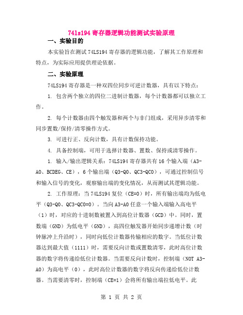
74ls194寄存器逻辑功能测试实验原理一、实验目的本实验旨在测试74LS194寄存器的逻辑功能,了解其工作原理和特点,为实际应用提供理论依据。
二、实验原理74LS194寄存器是一种双四位同步可逆计数器,具有以下特点:1. 包含两个独立的四位二进制计数器,每个计数器都可以独立工作。
2. 每个计数器由四个触发器和两个与非门组成,采用异步清零和同步置数/保持/清零操作方式。
3. 可进行正、反向计数,具有计数保持功能。
4. 具备控制端,可用于选择计数器、置数、保持或清零操作。
1. 输入/输出逻辑关系:74LS194寄存器共有16个输入端(A3-A0、BCDEG、CE),6个输出端(Q3-Q0、QC3-QC0),可通过控制信号和输入信号的变化,观察输出端的变化情况,从而测试其逻辑功能。
2. 工作原理:当74LS194复位(CE=0)时,所有输出端均为低电平(Q3-Q0、QC3-QC0=0)。
当向A3-A0任意一个输入端输入高电平(1)时,对应的十进制数被置入到高位计数器(GCD)中。
同时,置数端(GND)为低电平(GND),高四位触发器开始同步递增计数(时钟脉冲上升沿时),同时向低位计数器传输相应的数字。
当低位计数器达到最大值(1111)时,需要反向计数或置数清零,此时高位计数器的数字将传递给低位计数器。
当需要反向计数时,控制端(NOT A3-A0)为高电平(0),此时高位计数器的数字将反向传递给低位计数器。
当需要清零时,控制端(CE=1)会将所有输出端拉低电平。
此外,控制端还可以选择保持或清零操作,保持状态时,当时钟脉冲上升沿来临时,高四位触发器将按原方向继续递增计数;当处于清零状态时,所有输出端被强制拉低电平。
三、实验步骤1. 准备实验器材:74LS194寄存器芯片、测试板、电源模块、连接线等。
2. 连接电路:将74LS194芯片焊接在测试板上,根据其引脚定义连接相应的电源线和数据线。
3. 输入测试信号:通过控制台输入控制信号和输入信号,观察输出端的变化情况。
74HC244中文资料

-12
mA
74
-15
输出低电平电流IOL
54
12
mA
74
24
动态特性(TA=25℃)
参数
测试条件
LS244
单位
最大
tPLH输出由低到高传输延迟时间
Vcc =5V
CL=45pF
RL=667Ω
18
ns
tPHL输出由高到低传输延迟时间
18
ns
tPZH输出由高阻态到高允许时间
23
ns
tPZL输出由高阻态到低允许时间
/1G, /2G三态允许端(低电平有效)
1Y1~1Y4,2Y1~2Y4输出端
逻辑图:
双列直插封装
极限值:
电源电压………………………………………….7V
输入电压………………………………………….5.5V
输出高阻态时高电平电压………………………….5.5V
工作环境温度
54XXX………………………………….-55~125℃
1Y,2Y均为低电平
46
1Y,2Y均为高阻态
54
[1]:测试条件中的“最小”和“最大”用推荐工作条件中的相应值。
54/74LS244
三态八缓冲器/线驱动器/线接收器(3S,两组控制)
简要说明:
244为三态输出的八组缓冲器和总线驱动器,其主要电器特性的典型值如下(不同厂家具体值有差别):
型号
tPLH
tphl
PD
54LS241/74LS241
12ns
12ns
110mW
引出端符号:
1A1~1A4,2A1~2A4输入端
30
ns
tPHZ输出由高到高阻态禁止时间
- 1、下载文档前请自行甄别文档内容的完整性,平台不提供额外的编辑、内容补充、找答案等附加服务。
- 2、"仅部分预览"的文档,不可在线预览部分如存在完整性等问题,可反馈申请退款(可完整预览的文档不适用该条件!)。
- 3、如文档侵犯您的权益,请联系客服反馈,我们会尽快为您处理(人工客服工作时间:9:00-18:30)。
August 1986Revised March 2000DM74LS240 • DM74LS241Octal 3-STATE Buffer/Line Driver/Line ReceiverDM74LS240 •General DescriptionThese buffers/line drivers are designed to improve both the performance and PC board density of 3-STATE buffers/ drivers employed as memory-address drivers, clock driv-ers, and bus-oriented transmitters/receivers. Featuring 400 mV of hysteresis at each low current PNP data line input, they provide improved noise rejection and high fanout outputs and can be used to drive terminated lines down to 133Ω. Features■3-STATE outputs drive bus lines directly■PNP inputs reduce DC loading on bus lines■Hysteresis at data inputs improves noise margins■Typical I OL (sink current)24mA■Typical I OH (source current)-15 mA■ Typical propagation delay timesInverting 10.5 nsNoninverting 12 ns■Typical enable/disable time 18 ns■Typical power dissipation (enabled)Inverting 130 mW Noninverting 135 mW DM74LS241 Octal 3-STATE Buffer/LineOrdering Code:Order Number Package Number Package DescriptionDM74LS240WM M20B 20-Lead Small Outline Integrated Circuit (SOIC), JEDEC MS-013, 0.300 WideDM74LS240SJ M20D 20-Lead Small Outline Package (SOP), EIAJ TYPE II, 5.3mm WideDM74LS240N N20A 20-Lead Plastic Dual-In-Line Package (PDIP), JEDEC MS-001, 0.300 WideDM74LS241WM M20B 20-Lead Small Outline Integrated Circuit (SOIC), JEDEC MS-013, 0.300 WideDM74LS241N N20A 20-Lead Plastic Dual-In-Line Package (PDIP), JEDEC MS-001, 0.300 WideDevices also available in Tape and Reel. Specify by appending the suffix letter “X” to the ordering code.Connection DiagramsDM74LS240 DM74LS241Driver/Line Receiver © 2000 Fairchild Semiconductor Corporation D M 74L S 240 • D M 74L S 241Function TablesDM74LS240InputsOutputGAYL L H L H LHXZL = LOW Logic LevelH = HIGH Logic LevelX = Either LOW or HIGH Logic LevelZ = High ImpedanceDM74LS241InputsOutputsGG1A2A1Y2YX L L X LX L H X H XH X X ZHX X LL H X X H H LXXXZ2Absolute Maximum Ratings(Note 1)Supply Voltage 7V Note 1: The “Absolute Maximum Ratings” are those values beyond which the safety of the device cannot be guaranteed. The device should not beInput Voltage 7V operated at these limits. The parametric values defined in the ElectricalCharacteristics tables are not guaranteed at the absolute maximum ratings. Operating Free Air Temperature Range 0︒C to +70︒C The “Recommended Operating Conditions” table will define the conditions Storage Temperature Range -65︒C to +150︒C for actual device operation.Recommended Operating ConditionsSymbol Parameter Min Nom Max Units VCC Supply Voltage 4.75 5 5.25 VVIH HIGH Level Input Voltage 2 VVIL LOW Level Input Voltage 0.8 VIOH HIGH Level Output Current -15 mA IOL LOW Level Output Current 24 mA TA Free Air Operating Temperature 0 70 ︒C Electrical Characteristicsover recommended operating free air temperature range (unless otherwise noted)Symbol Parameter Conditions MinTypMax Units (Note 2)VI Input Clamp Voltage V CC= Min, I I= -18 mA -1.5 VHYS Hysteresis (V T+- V T-) VCC= Min 0.2 0.4 V Data Inputs OnlyVOH HIGH Level Output Voltage V CC= Min, V IH= Min 2.7V IL= Max, I OH= -1 mAV CC= Min, V IH= Min 2.4 3.4 VV IL= Max, I OH= -3 mAV CC= Min, V IH= Min 2V IL= 0.5V, I OH= MaxVOL LOW Level Output Voltage V CC= Min I OL= 12 mA 0.4V IL= Max IOL = Max 0.5 VV IH= MinIOZH Off-State Output Current, V CC= Max VO = 2.7V 20 μA HIGH Level Voltage Applied V IL= MaxIOZL Off-State Output Current, V IH= Min VO = 0.4V -20 μA LOW Level Voltage AppliedI I Input Current at Maximum V CC= Max 0.1 mAInput Voltage V I= 7VIIH HIGH Level Input Current V CC= Max, V I= 2.7V 20 μA IIL LOW Level Input Current V CC= Max, V I= 0.4V -0.2 mA IOS Short Circuit Output Current V CC= Max (Note 3) -40 -225 mA ICC Supply Current V CC= Max, Outputs HIGH 13 23Outputs OPENOutputs LOW 26 4427 46 mAOutputs Disabled 29 50 32 54Note 2: All typicals are at V CC= 5V, T A= 25︒C.Note 3: Not more than one output should be shorted at a time, and the duration should not exceed one second.DM74LS240 • DM74LS241D M 74L S 240 • D M 74L S 241Switching Characteristics at V CC = 5V and T A = 25︒CSymbolParameterConditionsMaxUnitstPLH Propagation Delay Time C L = 45 pFDM74LS240 14 ns LOW-to-HIGH Level Output R L = 667Ω DM74LS241 18tPHLPropagation Delay Time C L = 45 pFDM74LS240 18 ns HIGH-to-LOW Level Output R L = 667Ω DM74LS241 18t PZLOutput Enable Time C L = 45 pFDM74LS240 30 ns to LOW Level R L = 667Ω DM74LS241 30tPZHOutput Enable Time C L = 45 pFDM74LS240 23 ns to HIGH Level R L = 667Ω DM74LS241 23t PLZOutput Disable Time C L = 5 pFDM74LS240 25 ns from LOW Level R L = 667Ω DM74LS241 25tPHZOutput Disable Time C L = 5 pFDM74LS240 18 ns from HIGH Level R L = 667Ω DM74LS241 18t PLHPropagation Delay Time C L = 150 pFDM74LS240 18 ns LOW-to-HIGH Level Output R L = 667Ω DM74LS241 21tPHLPropagation Delay Time C L = 150 pFDM74LS240 22 ns HIGH-to-LOW Level Output R L = 667Ω DM74LS241 22tPZLOutput Enable Time C L = 150 pFDM74LS240 33 ns to LOW Level R L = 667Ω DM74LS241 33tPZHOutput Enable Time C L = 150 pFDM74LS240 26 ns to HIGH LevelR L = 667ΩDM74LS241264DM74LS240 • DM74LS241 Physical Dimensions inches (millimeters) unless otherwise noted20-Lead Small Outline Integrated Circuit (SOIC), JEDEC MS-013, 0.300 WidePackage Number M20BD M 74L S 240 • D M 74L S 241Physical Dimensions inches (millimeters) unless otherwise noted (Continued)20-Lead Small Outline Package (SOP), EIAJ TYPE II, 5.3mm WidePackage Description M20D6Physical Dimensions inches (millimeters) unless otherwise noted (Continued)20-Lead Plastic Dual-In-Line Package (PDIP), JEDEC MS-001, 0.300 WidePackage Number N20AFairchild does not assume any responsibility for use of any circuitry described, no circuit patent licenses are implied and Fairchild reserves the right at any time without notice to change said circuitry and specifications.LIFE SUPPORT POLICYFAIRCHILD’S PRODUCTS ARE NOT AUTHORIZED FOR U SE AS CRITICAL COMPONENTS IN LIFE SUPPORT DEVICES OR SYSTEMS WITHOUT THE EXPRESS WRITTEN APPROVAL OF THE PRESIDENT OF FAIRCHILD SEMICONDUCTOR CORPORATION. As used herein:1. Life support devices or systems are devices or systems2. A critical component in any component of a life supportwhich, (a) are intended for surgical implant into the device or system whose failure to perform can be rea- body, or (b) support or sustain life, and (c) whose failure sonably expected to cause the failure of the life support to perform when properly used in accordance with device or system, or to affect its safety or effectiveness.instructions for use provided in the labeling, can be rea-sonably expected to result in a significant injury to the user. DM74LS240 • DM74LS241 Octal 3 -STATE Buffer/Line Driver/Line Receiver。