SN74ABT125QDRQ1,SN74ABT125QDRG4Q1, 规格书,Datasheet 资料
TI模拟器件, TI半导体, TI数字信号处理 - 德州仪器 处理器 宽带 RF IF 和数字音频广播
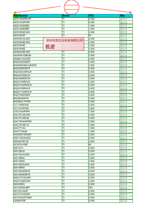
LM2903DR TI2,500茂百兴LM2903PWR TI2,000茂百兴LM3S1601-IQC50-A2T TI1,000茂百兴LM3S1607-IQR50-A0T TI1,500茂百兴LM3S1911-IQC50-A2T TI1,000茂百兴LM3S1968-IQC50-A2T TI1,000茂百兴LM3S2793-IQC80-C3T TI1,000茂百兴LM3S2965-IQC50-A2T TI1,000茂百兴LM3S3749-IQC50-A0T TI1,000茂百兴LM3S6911-IQC50-A2T TI1,000茂百兴LM3S9B90-IQC80-C3T TI1,000茂百兴LM3S9B92-IQC80-C1TI90茂百兴LM3S9B92-IQC80-C3TI90茂百兴LM4040C50IDBZR TI3,000茂百兴LM4041C12IDCKR TI3,000茂百兴LMV321IDBVR TI3,000茂百兴LMV324IPWR TI2,000茂百兴LMV331IDCKR TI3,000茂百兴LT1013DDR TI2,500茂百兴MAX3221CDBR TI2,000茂百兴MAX3221CPWR TI2,000茂百兴MAX3221IPWR TI2,000茂百兴MAX3223ECDBR TI2,000茂百兴MAX3232CDBR TI2,000茂百兴MAX3232CPWR TI2,000茂百兴MAX3232ECDBR TI2,000茂百兴MAX3232IPWR TI2,000茂百兴MAX3238EIPWR TI2,000茂百兴MAX3243CDBR TI2,000茂百兴MAX3243CPWR TI2,000茂百兴MAX3243ECDBR TI2,000茂百兴MAX3243ECPWR TI2,000茂百兴MSC1211Y5PAGR TI1,500茂百兴MSP430F1232IPWR TI2,000茂百兴MSP430F135IPMR TI1,000茂百兴MSP430F149IPMR TI1,000茂百兴MSP430F1611IPMR TI1,000茂百兴MSP430F1612IPMR TI1,000茂百兴MSP430F169IPMR TI1,000茂百兴MSP430F2001IPWR TI2,000茂百兴MSP430F2011TPWR TI2,000茂百兴MSP430F2132IPMR TI2,000茂百兴MSP430F2232IDAR TI2,000茂百兴MSP430F2252IRHAR TI2,500茂百兴MSP430F413IPMR TI1,000茂百兴MSP430F4250IRGZR TI2,500茂百兴MSP430F5418IPNR TI1,000茂百兴ONET1101LRGER TI3,000茂百兴ONET8501PRGTR TI3,000茂百兴ONET8501VRGPR TI3,000茂百兴OPA2131UA TI2,500茂百兴OPA2132UA TI2,500茂百兴OPA2134UA TI2,500茂百兴OPA2227UA TI2,500茂百兴OPA2244EA TI2,500茂百兴OPA2277UA TI2,500茂百兴OPA2335AIDR TI2,500茂百兴OPA2343EA/2K5TI2,500茂百兴OPA2348AIDCNR TI3,000茂百兴OPA2348AIDR TI3,000茂百兴OPA2349EA/3K TI3,000茂百兴OPA2350UA TI2,500茂百兴OPA2354AIDGKR TI2,500茂百兴OPA2357AIDGSR TI2,500茂百兴OPA2364AIDGKR TI2,500茂百兴OPA2364IDGKR TI2,500茂百兴OPA277AIDRMR TI3,000茂百兴OPA277U TI2,500茂百兴OPA277UA TI2,500茂百兴OPA334AIDBVR TI3,000茂百兴OPA335AIDBVR TI3,000茂百兴OPA336N TI3,000茂百兴OPA340UA/2K5TI2,500茂百兴OPA348AIDBVR TI3,000茂百兴OPA361AIDCKR TI3,000茂百兴OPA374AIDBVR TI3,000茂百兴OPA376AIDBVR TI3,000茂百兴OPA4227UA/2K5TI2,500茂百兴OPA4340UA/2k5TI2,500茂百兴OPA846IDBVR TI3,000茂百兴PCI1510PGE TI60茂百兴PCI1520ZHK TI90茂百兴PCI2040PGE TI60茂百兴PCI2050BIPDV TI36茂百兴PCI2050BIZHK TI450茂百兴PCI2050BPDV TI360茂百兴PCI2050BZHK TI450茂百兴PCI2050IBPDV TI360茂百兴PCI2250PCM TI24茂百兴PCI8402ZHK TI90茂百兴PCI8412ZHK TI90茂百兴PCM1742KE/2K TI2,000茂百兴PCM1753DBQR TI2,000茂百兴PCM1754DBQR TI2,000茂百兴PCM1755DBQR TI2,000茂百兴PCM1808PWR TI2,000茂百兴PCM4104PFBR TI2,000茂百兴PCM4204PAPR TI1,500茂百兴PTH08T220WAZT TI250茂百兴PTH08T260WAZT TI250茂百兴REF3025AIDBZR TI3,000茂百兴REF3030AIDBZR TI3,000茂百兴REF3033AIDBZR TI3,000茂百兴SN65176BDR TI2,500茂百兴SN65220DBVR TI3,000茂百兴SN65240PWR TI2,000茂百兴SN65HVD10DR TI2,500茂百兴SN65HVD11DR TI2,500茂百兴SN65HVD230DR TI2,500茂百兴SN65HVD23DR TI2,500茂百兴SN65HVD251DR TI2,500茂百兴SN65HVD3082EDR TI2,500茂百兴SN65HVD3088EDGKR TI2,500茂百兴SN65HVD33DR TI2,500茂百兴SN65LVDS2DBVR TI3,000茂百兴SN65MLVD200ADR TI2,500茂百兴SN7406DR TI2,500茂百兴SN7407DR TI2,500茂百兴SN74ABTE16246DGGR TI2,000茂百兴SN74AC14PWR TI2,000茂百兴SN74AHC14PWR TI2,000茂百兴SN74AHC1G14DBVR TI3,000茂百兴SN74AHCT08DGVR TI2,000茂百兴SN74AHCT132DR TI2,500茂百兴SN74ALVC164245DLR TI1,000茂百兴SN74ALVCH162244GR TI2,000茂百兴SN74ALVCH162373GR TI2,000茂百兴SN74AUP1G125DCKR TI3,000茂百兴SN74AVC2T45DCUR TI3,000茂百兴SN74CB3Q3257PWR TI2,000茂百兴SN74CBTLV3125PWR TI2,000茂百兴SN74HC14DR TI2,500茂百兴SN74HC164PWR TI2,000茂百兴SN74HC165DR TI2,500茂百兴SN74HC590ADR TI2,500茂百兴SN74HCT541PWR TI2,000茂百兴SN74LV07APWR TI2,000茂百兴SN74LV08APWR TI2,000茂百兴SN74LV14APWR TI2,000茂百兴SN74LV164APWR TI2,000茂百兴SN74LV244ADWR TI2,000茂百兴SN74LV244APWR TI2,000茂百兴SN74LV32APWR TI2,000茂百兴SN74LV595APWR TI2,000茂百兴SN74LV595ARGYR TI1,000茂百兴SN74LVC04ADR TI2,500茂百兴SN74LVC04APWR TI2,000茂百兴SN74LVC08APWR TI2,000茂百兴SN74LVC125APWR TI2,000茂百兴SN74LVC138APWR TI2,000茂百兴SN74LVC14ADR TI2,500茂百兴SN74LVC14APWR TI2,000茂百兴SN74LVC16244ADLR TI1,000茂百兴SN74LVC16245ADGGR TI2,000茂百兴SN74LVC16373ADGGR TI2,000茂百兴SN74LVC1G07DCKR TI3,000茂百兴SN74LVC1G125DCKR TI3,000茂百兴SN74LVC244APWR TI2,000茂百兴SN74LVC245ADGVR TI2,000茂百兴SN74LVC245APWR TI2,000茂百兴SN74LVC2G17DBVR TI3,000茂百兴SN74LVC32APWR TI2,000茂百兴SN74LVC4245APWR TI2,000茂百兴SN74LVC8T245PWR TI2,000茂百兴SN74LVCH162244AGR TI2,000茂百兴SN74LVCH16244ADGGR TI2,000茂百兴SN74LVCH16245ADLR TI1,000茂百兴SN74LVCHR16245AGR TI2,000茂百兴SN74LVTH125PWR TI2,000茂百兴SN74LVTH162244DGGR TI2,000茂百兴SN74LVTH16244ADGGR TI2,000茂百兴SN74LVTH16244ADLR TI1,000茂百兴SN74LVTH16245ADLR TI1,000茂百兴SN74LVTH244APWR TI2,000茂百兴SN75240PWR TI2,000茂百兴SN75ALS1178NSR TI2,000茂百兴SN75LBC176ADR TI2,500茂百兴TAS1020BPFBR TI1,000茂百兴TAS5707PHPR TI1,000茂百兴TFP410PAP TI160茂百兴THS7314DR TI2,500茂百兴THS7316DR TI2,500茂百兴THS7374IPWR TI2,000茂百兴THS8134BCPHP TI250茂百兴THS8200PFP TI96茂百兴TL16C2550PFBR TI1,000茂百兴TL16C550CIPTR TI1,000茂百兴TL16C550CPTR TI1,000茂百兴TL16C550CPTR TI1,000茂百兴TL16C554AFNR TI250茂百兴TL16C554AIPNR TI1,000茂百兴TL16C554APNR TI1,000茂百兴TL16C752BPTR TI1,000茂百兴TL431AIDBVR TI3,000茂百兴TL431IDBVR TI3,000茂百兴TL7705ACDR TI2,500茂百兴TL7712ACDR TI2,500茂百兴TLC1543CDWR TI2,000茂百兴TLC2252AIDR TI2,500茂百兴TLC2252CDR TI2,500茂百兴TLC2254IDR TI2,500茂百兴TLC2262CDR TI2,500茂百兴TLC2272CDR TI2,500茂百兴TLC2274ACDR TI2,500茂百兴TLC2543CDBR TI2,000茂百兴TLC2543CDWR TI2,000茂百兴TLC25M2CDR TI2,500茂百兴TLC3548IDWR TI2,000茂百兴TLC3548IPWR TI2,000茂百兴TLC3702IDR TI2,500茂百兴TLC5510INSR TI2,000茂百兴TLC555CDR TI2,500茂百兴TLC555IDR TI2,500茂百兴TLC5602CDWR TI2,000茂百兴TLC5946RHBR TI3,000茂百兴TLC7701IDR TI2,500茂百兴TLE2062ACDR TI2,500茂百兴TLE2072CDR TI2,500茂百兴TLK1501IRCPR TI1,000茂百兴TLV1543CDWR TI2,000茂百兴TLV2211IDBVR TI3,000茂百兴TLV2231IDBVR TI3,000茂百兴TLV2371IDBVR TI3,000茂百兴TLV2372IDGKR TI2,500茂百兴TLV2432AIDR TI2,500茂百兴TLV2442CDR TI2,500茂百兴TLV2462IDGKR TI2,500茂百兴TLV2556IPWR TI2,000茂百兴TLV272CDR TI2,500茂百兴TLV274CPWR TI2,000茂百兴TLV320AIC1106PWR TI2,000茂百兴TLV320AIC12IDBTR TI2,000茂百兴TLV320AIC3104IRHBR TI3,000茂百兴TLV320AIC31IRHBR TI3,000茂百兴TLV320AIC32IRHBR TI3,000茂百兴TLV320AIC33IZQER TI2,500茂百兴TLV431ACDBVR TI3,000茂百兴TMDS442PNPR TI1,000茂百兴TMP100NA TI3,000茂百兴TMP101NA TI3,000茂百兴TMP20AIDCKR TI3,000茂百兴TMP275AIDR TI2,500茂百兴TMP411ADR TI2,500茂百兴TMP75AIDGKR TI2,500茂百兴TMP75AIDR TI2,500茂百兴TMS320C32PCM50TI24茂百兴TMS320C6205ZHK200TI90茂百兴TMS320C6211BZFN167TI40茂百兴TMS320C6713BGDP225TI40茂百兴TMS320C6713BZDP225TI40茂百兴TMS320C6713BZDP300TI40茂百兴TMS320C6727BZDH300TI90茂百兴TMS320DM355ZCE216TI160茂百兴TMS320DM355ZCE270TI160茂百兴TMS320DM365ZCE27TI160茂百兴TMS320DM365ZCE30TI160茂百兴TMS320DM642AZDK6TI60茂百兴TMS320DM642AZDK7TI60茂百兴TMS320DM642AZNZ7TI40茂百兴TMS320DM6441AZWT TI90茂百兴TMS320DM6446AZWT TI90茂百兴TMS320DM6467TZUT1TI84茂百兴TMS320DM648ZUT9TI84茂百兴TMS320F28015PZA TI90茂百兴TMS320F2802PZA TI90茂百兴TMS320F2806PZA TI90茂百兴TMS320F2808PZA TI90茂百兴TMS320F2810PBKA TI90茂百兴TMS320F2811PBKA TI90茂百兴TMS320F2812GHHA TI160茂百兴TMS320F2812PGFA TI40茂百兴TMS320F28335PGFA TI40茂百兴TMS320LC549PGE-80TI60茂百兴TMS320LF2401AVFA TI250茂百兴TMS320LF2406APZA TI90茂百兴TMS320LF2407APGEA TI60茂百兴TMS320VC33PGE120TI60茂百兴TMS320VC33PGE150TI60茂百兴TMS320VC33PGEA120TI60茂百兴TMS320VC5402PGE100TI60茂百兴TMS320VC5409APGE16TI60茂百兴TMS320VC5409PGE80TI60茂百兴TMS320VC5410APGE16TI60茂百兴TMS32C6713BGDPA200TI40茂百兴TPA2005D1DRBR TI3,000茂百兴TPA2008D2PWPR TI2,000茂百兴TPA2010D1YZFR TI2,500茂百兴TPA2012D2RTJR TI3,000茂百兴TPA2013D1RGPR TI3,000茂百兴TPA3001D1PWPR TI2,000茂百兴TPA3007D1PWR TI2,000茂百兴TPA3100D2PHPR TI1,000茂百兴TPA3101D2PHPR TI1,000茂百兴TPA3110D2PWPR TI2,000茂百兴TPA3113D2PWPR TI2,000茂百兴TPA3120D2PWPR TI2,000茂百兴TPA3121D2PWPR TI2,000茂百兴TPA3123D2PWPR TI2,000茂百兴TPA3123D2PWPR TI2,000茂百兴TPA3124D2PWPR TI2,000茂百兴TPA6011A4PWPR TI2,000茂百兴TPA6110A2DGNR TI2,500茂百兴TPA6111A2DGNR TI2,500茂百兴TPA6111A2DR TI2,500茂百兴TPA6112A2DGQR TI2,500茂百兴TPA6132A2RTER TI3,000茂百兴TPA6204A1DRBR TI3,000茂百兴TPA6211A1DGNR TI2,500茂百兴TPA6211A1DRBR TI3,000茂百兴TPD12S520DBTR TI2,000茂百兴TPIC6595DWR TI2,000茂百兴TPIC6B595DWR TI2,000茂百兴TPS2034DR TI2,500茂百兴TPS2041BDBVR TI3,000茂百兴TPS2041BDR TI2,500茂百兴TPS2042BDGNR TI2,500茂百兴TPS2042BDR TI2,500茂百兴TPS2044BDR TI2,500茂百兴TPS2051BDBVR TI3,000茂百兴TPS2051BDGNR TI2,500茂百兴TPS2051BDR TI2,500茂百兴TPS2052BDR TI2,500茂百兴TPS2061DGN TI80茂百兴TPS2105DBVR TI3,000茂百兴TPS2113APWR TI2,000茂百兴TPS2115PWR TI2,000茂百兴TPS2320IPWR TI2,000茂百兴TPS2331IPWR TI2,000茂百兴TPS2350PW TI2,000茂百兴TPS23750PWPR TI2,000茂百兴TPS23753PWR TI2,000茂百兴TPS23754PWPR TI2,000茂百兴TPS2375DR TI2,500茂百兴TPS23770PWPR TI2,000茂百兴TPS2390DGKR TI2,500茂百兴TPS2391DGKR TI2,500茂百兴TPS2551DRVR TI3,000茂百兴TPS2553DBVR TI3,000茂百兴TPS2553DRVR TI3,000茂百兴TPS2812DR TI2,500茂百兴TPS2814DR TI2,500茂百兴TPS2814PWR TI2,000茂百兴TPS2829DBVR TI3,000茂百兴TPS3106E09DBVR TI3,000茂百兴TPS3106K33DBVR TI3,000茂百兴TPS3305-18DR TI2,500茂百兴TPS3307-18DR TI2,500茂百兴TPS3619-33DGKR TI2,500茂百兴TPS3620-33DGKR TI2,500茂百兴TPS3707-33DR TI2,500茂百兴TPS3801E18DCKR TI3,000茂百兴TPS3801J25DCKR TI3,000茂百兴TPS3801K33DCKR TI3,000茂百兴TPS3803-01DCKR TI3,000茂百兴TPS3808G01DBVR TI3,000茂百兴TPS3808G18DBVR TI3,000茂百兴TPS3808G33DBVR TI3,000茂百兴TPS3809K33DBVR TI3,000茂百兴TPS3820-33DBVR TI3,000茂百兴TPS3823-33DBVR TI3,000茂百兴TPS3824-33DBVR TI3,000茂百兴TPS3825-33DBVR TI3,000茂百兴TPS3828-33DBVR TI3,000茂百兴TPS3828-50DBVR TI3,000茂百兴TPS40001DGQR TI2,500茂百兴TPS40009DGQR TI2,500茂百兴TPS40021PWPR TI2,000茂百兴TPS40041DRBR TI3,000茂百兴TPS40055PWPR TI2,000茂百兴TPS40056PWPR TI2,000茂百兴TPS40057PWPR TI2,000茂百兴TPS40060PWPR TI2,000茂百兴TPS40061PWPR TI2,000茂百兴TPS40071PWPR TI2,000茂百兴TPS40077PWPR TI2,000茂百兴TPS40100RGER TI3,000茂百兴TPS40101RGER TI3,000茂百兴TPS40130DBTR TI2,000茂百兴TPS40190DRCR TI2,500茂百兴TPS40192DRCR TI3,000茂百兴TPS40200DR TI2,500茂百兴TPS40210DGQR TI2,500茂百兴TPS40222DRPR TI3,000茂百兴TPS51100DGQR TI2,500茂百兴TPS51116PWPR TI2,000茂百兴TPS51116RGER TI3,000茂百兴TPS51117RGYR TI3,000茂百兴TPS51120RHBR TI3,000茂百兴TPS51200DRCR TI3,000茂百兴TPS51218DSCR TI3,000茂百兴TPS54010PWPR TI2,000茂百兴TPS5410DR TI2,500茂百兴TPS54110PWPR TI2,000茂百兴TPS54140DGQR TI2,500茂百兴TPS54160DGQR TI2,500茂百兴TPS5420DR TI2,500茂百兴TPS54226PWPR TI2,000茂百兴TPS54231DR TI2,500茂百兴TPS54283PWPR TI2,000茂百兴TPS54286PWPR TI2,000茂百兴TPS54292PWPR TI2,000茂百兴TPS5430DDAR TI2,500茂百兴TPS54310PWPR TI2,000茂百兴TPS54314PWPR TI2,000茂百兴TPS54319RTER TI3,000茂百兴TPS54325PWPR TI2,000茂百兴TPS54331DR TI2,500茂百兴TPS54350PWPR TI2,000茂百兴TPS54357PWPR TI2,000茂百兴TPS54372PWPR TI2,000茂百兴TPS54380PWPR TI2,000茂百兴TPS54383PWPR TI2,000茂百兴TPS54386PWPR TI2,000茂百兴TPS54418RTER TI3,000茂百兴TPS5450DDAR TI2,500茂百兴TPS54550PWPR TI2,000茂百兴TPS54610PWPR TI2,000茂百兴TPS54612PWPR TI2,000茂百兴TPS54614PWPR TI2,000茂百兴TPS54616PWPR TI2,000茂百兴TPS54620RGYR TI3,000茂百兴TPS54672PWPR TI2,000茂百兴TPS54680PWPR TI2,000茂百兴TPS54910PWPR TI2,000茂百兴TPS54972PWPR TI2,000茂百兴TPS60150DRVR TI3,000茂百兴TPS60230RGTR TI3,000茂百兴TPS60231RGTR TI3,000茂百兴TPS60400DBVR TI3,000茂百兴TPS60403DBVR TI3,000茂百兴TPS60500DGSR TI2,500茂百兴TPS61020DRCR TI3,000茂百兴TPS61026DRCR TI3,000茂百兴TPS61030PWPR TI2,000茂百兴TPS61030RSAR TI2,000茂百兴TPS61032PWPR TI2,000茂百兴TPS61040DBVR TI3,000茂百兴TPS61041DBVR TI3,000茂百兴TPS61042DRBR TI3,000茂百兴TPS61045DRBR TI3,000茂百兴TPS61050YZGR TI3,000茂百兴TPS61070DDCR TI3,000茂百兴TPS61080DRCR TI3,000茂百兴TPS61081DRCR TI3,000茂百兴TPS61087DRCR TI3,000茂百兴TPS61090RSAR TI3,000茂百兴TPS61097-33DBVR TI3,000茂百兴TPS61160DRVR TI3,000茂百兴TPS61161DRVR TI3,000茂百兴TPS61165DRVR TI3,000茂百兴TPS62000DGSR TI2,500茂百兴TPS62040DGQR TI2,500茂百兴TPS62040DRCR TI3,000茂百兴TPS62046DGQR TI2,500茂百兴TPS62050DGSR TI2,500茂百兴TPS62060DSGR TI3,000茂百兴TPS62110RSAR TI3,000茂百兴TPS62111RSAR TI3,000茂百兴TPS62200DBVR TI3,000茂百兴TPS62201DBVR TI3,000茂百兴TPS62202DBVR TI3,000茂百兴TPS62203DBVR TI3,000茂百兴TPS62204DBVR TI3,000茂百兴TPS62260DDCR TI3,000茂百兴TPS62260DRVR TI3,000茂百兴TPS62290DRVR TI3,000茂百兴TPS62410DRCR TI3,000茂百兴TPS62510DRCR TI3,000茂百兴TPS62590DRVR TI3,000茂百兴TPS63000DRCR TI3,000茂百兴TPS63001DRCR TI3,000茂百兴TPS63020DSJR TI3,000茂百兴TPS63021DSJR TI3,000茂百兴TPS63030DSKR TI3,000茂百兴TPS63031DSKR TI3,000茂百兴TPS63700DRCR TI3,000茂百兴TPS64200DBVR TI3,000茂百兴TPS64202DBVR TI3,000茂百兴TPS65020RHAR TI2,500茂百兴TPS65021RHAR TI2,500茂百兴TPS65023RSBR TI3,000茂百兴TPS650243RHBR TI3,000茂百兴TPS65053RGER TI3,000茂百兴TPS65120RGTR TI3,000茂百兴TPS65150PWPR TI2,000茂百兴TPS65251RHAR TI2,500茂百兴TPS65920BZCHR TI2,000茂百兴TPS65930BZCHR TI1,000茂百兴TPS6755IDR TI2,500茂百兴TPS70102PWPR TI2,000茂百兴TPS70302PWPR TI2,000茂百兴TPS7101QDR TI2,500茂百兴TPS71501DCKR TI3,000茂百兴TPS71530DCKR TI3,000茂百兴TPS71533DCKR TI3,000茂百兴TPS71550DCKR TI3,000茂百兴TPS71701DCKR TI3,000茂百兴TPS72301DBVR TI3,000茂百兴TPS72501DCQR TI2,500茂百兴TPS72515DCQR TI2,500茂百兴TPS73018DBVR TI3,000茂百兴TPS73033DBVR TI3,000茂百兴TPS73101DBVR TI3,000茂百兴TPS73115DBVR TI3,000茂百兴TPS73130DBVR TI3,000茂百兴TPS73133DBVR TI3,000茂百兴TPS73201DBVR TI3,000茂百兴TPS73601DBVR TI3,000茂百兴TPS73601DCQR TI3,000茂百兴TPS73633DRBR TI3,000茂百兴TPS73701DCQR TI2,500茂百兴TPS73701DRBR TI3,000茂百兴TPS74401RGWR TI3,000茂百兴TPS74701DRCR TI3,000茂百兴TPS74801DRCR TI3,000茂百兴TPS75201QPWPR TI2,000茂百兴TPS76050DBVR TI3,000茂百兴TPS76301DBVR TI3,000茂百兴TPS76318DBVR TI3,000茂百兴TPS76333DBVR TI3,000茂百兴TPS76350DBVR TI3,000茂百兴TPS76633DR TI2,500茂百兴TPS76650DR TI2,500茂百兴TPS76701QPWPR TI2,000茂百兴TPS767D318PWPR TI2,000茂百兴TPS76801QDR TI2,500茂百兴TPS76933DBVR TI3,000茂百兴TPS77601PWPR TI2,000茂百兴TPS77633DR TI2,500茂百兴TPS77701PWPR TI2,000茂百兴TPS77801PWPR TI2,000茂百兴TPS78833DBVR TI3,000茂百兴TPS79101DBVR TI3,000茂百兴TPS79301DBVR TI2,500茂百兴TPS79318DBVR TI3,000茂百兴TPS793285DBVR TI3,000茂百兴TPS79328DBVR TI3,000茂百兴TPS79330DBVR TI3,000茂百兴TPS79333DBVR TI3,000茂百兴TPS79501DCQR TI2,500茂百兴TPS79533DCQR TI2,500茂百兴TPS79633DCQR TI2,500茂百兴TPS79730DCKR TI3,000茂百兴TPS79901DDCR TI3,000茂百兴TS3USB221DRCR TI3,000茂百兴TS5A3167DBVR TI3,000茂百兴TSB12LV26PZT TI90茂百兴TSB43AB22APDT TI90茂百兴TSC2003IPWR TI2,500茂百兴TSC2007IPWR TI2,000茂百兴TSC2007IYZGR TI3,000茂百兴TSC2017IYZGR TI3,000茂百兴TSC2046IPWR TI2,500茂百兴TUSB2046BIVFR TI1,000茂百兴TUSB2046BVFR TI1,000茂百兴TUSB3200ACPAHR TI1,500茂百兴TUSB3410VF TI250茂百兴TVP5150AM1PBSR TI1,000茂百兴TVP5154APNPR TI1,000茂百兴TVP5158IPNPR TI1,000茂百兴TVP5158PNPR TI1,000茂百兴UC2637DWTR TI2,000茂百兴UC2825ADWTR TI2,000茂百兴UC2842AD8TR TI2,500茂百兴UC2843AD8TR TI2,500茂百兴UC2844AD8TR TI2,500茂百兴UC3637DWTR TI2,000茂百兴UC3825ADWTR TI2,000茂百兴UC3843AD8TR TI2,500茂百兴UC3845AD8TR TI2,500茂百兴UC3845AN TI50茂百兴UC3846DWTR TI2,000茂百兴UC3846N TI25茂百兴UC3854AN TI25茂百兴UC3854BDWTR TI2,000茂百兴UC3854N TI25茂百兴UC3902DTR TI2,500茂百兴UCC27223PWPR TI2,000茂百兴UCC27324DGNR TI2,500茂百兴UCC27324DR TI2,500茂百兴UCC27423DR TI2,500茂百兴UCC27424DR TI2,500茂百兴UCC2800DTR TI2,500茂百兴UCC28060DR TI2,500茂百兴UCC28061DR TI2,500茂百兴UCC28070PWR TI2,000茂百兴UCC2808APWTR-2TI2,000茂百兴UCC2809DTR-1TI2,500茂百兴UCC2809PTR-1TI2,500茂百兴UCC2818DTR TI2,500茂百兴UCC28600DR TI2,500茂百兴UCC2891PWR TI2,000茂百兴UCC2894DR TI2,500茂百兴UCC2895DWTR TI2,000茂百兴UCC2897APWR TI2,000茂百兴UCC28C43DR TI2,500茂百兴UCC28C44DR TI2,500茂百兴UCC28C45DR TI2,500茂百兴UCC37324DGNR TI2,500茂百兴UCC3801DTR TI2,500茂百兴UCC3807DTR-3TI2,500茂百兴UCC3808DTR-2TI2,500茂百兴UCC3818PWTR TI2,000茂百兴UCC3895DWTR TI2,000茂百兴UCC3895PWTR TI2,000茂百兴UCC3919DTR TI2,500茂百兴UCC3946DTR TI2,500茂百兴ULN2003ADR TI2,500茂百兴ULN2003AIDR TI2,500茂百兴ULN2003AN TI25茂百兴XIO1100GGB TI160茂百兴XTR116UA/2K5TI2,500茂百兴。
APT15GN120BD_SDQ1(G) 商品说明书

050-7598 R e v C 7-2009TYPICAL PERFORMANCE CURVESMAXIMUM RATINGSAll Ratings: T C = 25°C unless otherwise specifi ed.STATIC ELECTRICAL CHARACTERISTICSCharacteristic / Test ConditionsCollector-Emitter Breakdown Voltage (V GE = 0V , I C = 0.5mA)Gate Threshold Voltage (V CE = V GE , I C = 600µA, T j= 25°C)Collector-Emitter On Voltage (V GE = 15V , I C = 15A, T j = 25°C)Collector-Emitter On Voltage (V GE = 15V , I C = 15A, T j = 125°C)Collector Cut-off Current (V CE = 1200V , V GE = 0V , T j = 25°C) 2Collector Cut-off Current (V CE = 1200V , V GE = 0V , T j = 125°C) 2Gate-Emitter Leakage Current (V GE = ±20V)Intergrated Gate ResistorSymbol V (BR)CES V GE(TH)V CE(ON)I CES I GES R GINTUnitsVoltsµA nA ΩSymbol V CES V GE I C1I C2I CM SSOA P D T J ,T STGT LAPT15GN120BD_SDQ1(G)1200±3045224545A @ 1200V195-55 to 150300UNIT VoltsAmpsWatts °CParameterCollector-Emitter Voltage Gate-Emitter VoltageContinuous Collector Current @ T C = 25°C Continuous Collector Current @ T C = 110°C Pulsed Collector Current 1Switching Safe Operating Area @ T J = 150°C T otal Power DissipationOperating and Storage Junction T emperature RangeMax. Lead T emp. for Soldering: 0.063" from Case for 10 Sec.CAUTION: These Devices are Sensitive to Electrostatic Discharge. Proper Handling Procedures Should Be Followed.Utilizing the latest Field Stop and T rench Gate technologies, these IGBT's have ultralow V CE(ON) and are ideal for low frequency applications that require absolute minimum conduction loss. Easy paralleling is a result of very tight parameter distribution and a slightly positive V CE(ON) temperature coeffi cient. Low gate charge simplifi es gate drive design and minimizes losses.• 1200V Field Stop• Trench Gate: Low V CE(on) • Easy ParallelingApplications : Welding, Inductive Heating, Solar Inverters, SMPS, Motor drives, UPSMIN TYP MAX 12005.0 5.86.5 1.4 1.7 2.1 2.0200TBD 120N/AMicrosemi Website - APT15GN120BDQ1 APT15GN120SDQ1APT15GN120BDQ1(G) 1200V *G Denotes RoHS Compliant, Pb Free Terminal Finish.050-7598 R e v C 7-2009APT15GN120BD_SDQ1(G)1 Repetitive Rating: Pulse width limited by maximum junction temperature. 2 For Combi devices, I ces includes both IGBT and FRED leakages 3 See MIL-STD-750 Method 3471.4 E on1 is the clamped inductive turn-on energy of the IGBT only, without the effect of a commutating diode reverse recovery currentadding to the IGBT turn-on loss. Tested in inductive switching test circuit shown in fi gure 21, but with a Silicon Carbide diode.5 E on2 is the clamped inductive turn-on energy that includes a commutating diode reverse recovery current in the IGBT turn-on switchingloss. (See Figures 21, 22.)6 E off is the clamped inductive turn-off energy measured in accordance with JEDEC standard JESD24-1. (See Figures 21, 23.)7 R G is external gate resistance, not including R Gint nor gate driver impedance. (MIC4452)Microsemi Reserves the right to change, without notice, the specifi cations and information contained herein.THERMAL AND MECHANICAL CHARACTERISTICSUNIT °C/W gmMIN TYP MAX.641.185.9CharacteristicJunction to Case (IGBT)Junction to Case (DIODE)Package WeightSymbol R θJC R θJC W TDYNAMIC CHARACTERISTICSSymbol C ies C oes C res V GEP Q g Q ge Q gc SSOA t d(on)t r t d(off)t f E on1E on2E off t d(on)t r t d(off)t f E on1E on2E offTest Conditions Capacitance V GE = 0V , V CE = 25Vf = 1 MHz Gate Charge V GE = 15V V CE = 600V I C = 15AT J = 150°C, R G = 4.3Ω 7, V GE =15V , L = 100µH,V CE = 1200VInductive Switching (25°C)V CC = 800V V GE = 15V I C = 15A R G= 4.3Ω 7T J = +25°CInductive Switching (125°C)V CC = 800V V GE = 15V I C = 15A R G= 4.3Ω 7T J = +125°C Characteristic Input Capacitance Output CapacitanceReverse T ransfer Capacitance Gate-to-Emitter Plateau Voltage T otal Gate Charge 3 Gate-Emitter ChargeGate-Collector ("Miller") Charge Switching Safe Operating Area T urn-on Delay Time Current Rise Time T urn-off Delay Time Current Fall TimeT urn-on Switching Energy 4T urn-on Switching Energy (Diode) 5T urn-off Switching Energy 6 T urn-on Delay Time Current Rise Time T urn-off Delay Time Current Fall TimeT urn-on Switching Energy 4 4T urn-on Switching Energy (Diode) 55T urn-off Switching Energy 66MIN TYPMAX1200 65 50 9.0 90 5 55 4510 9 150 110 410 73095010 9 170 1854751310 1300UNITpFV nC Ans µJns µJ050-7598 R e v C 7-2009APT15GN120BD_SDQ1(G)TYPICAL PERFORMANCE CURVESV CE , COLLECTER-TO-EMITTER VOLT AGE (V)V CE , COLLECTER-TO-EMITTER VOLTAGE (V)FIGURE 1, Output Characteristics(T J = 25°C) FIGURE 2, Output Characteristics (T J = 125°C) V GE , GATE-TO-EMITTER VOLTAGE (V)GATE CHARGE (nC)FIGURE 3, Transfer CharacteristicsFIGURE 4, Gate ChargeV GE , GATE-TO-EMITTER VOLTAGE (V) T J , Junction Temperature (°C)FIGURE 5, On State Voltage vs Gate-to- Emitter VoltageFIGURE 6, On State Voltage vs Junction Temperature T J , JUNCTION TEMPERATURE (°C)T C , CASE TEMPERATURE (°C)FIGURE 7, Breakdown Voltage vs. Junction TemperatureFIGURE 8, DC Collector Current vs Case TemperatureB VC E S , C O L L E C T O R -T O -E M I T T E R B R E A KD O W N V CE , C O L L E C T O R -T O -E M I T T E R V O L T A G E (V )I C , C O L L E C T O R C U R R E N T (A )I C , C O L L E C T O R C U R R E N T (A )V O L T A G E (N O R M A L I Z E D )I C , D C C O L L E C T O R C U R R E N T (A ) V C E , C O L L E C T O R -T O -E M I T T E R V O L T A G E (V ) V G E , G A T E -T O -E M I T T E R V O L T A G E (V )I C , C O L L E C T O R C U R R E N T (A )1.101.051.000.950.90-50 -25 0 25 50 75 100 125-50 -25 0 25 50 75 100 125 150605040302010050-7598 R e v C 7-2009APT15GN120BD_SDQ1(G)S W I T C H I N G E N E R G Y L O S S E S (µJ ) E O N 2, T U R N O N E NE R G Y L O S S (µJ )t r , R I S E T I M E (n s )t d (O N ), T U R N -O N D E L A Y T I M E (ns )S W I T C H I N G E N E R G Y LO S S E S (µJ ) E O F F , T U R N O F F E N E R G YL O S S (µJ )t f , F A L L T I M E (n s )t d (O F F ), T U R N -O F FD E L A Y T I M E (n s )I CE , COLLECTOR TO EMITTER CURRENT (A) I CE , COLLECTOR TO EMITTER CURRENT (A) FIGURE 9, Turn-On Delay Time vs Collector Current FIGURE 10, Turn-Off Delay Time vs Collector Current I CE , COLLECTOR TO EMITTER CURRENT (A) I CE , COLLECTOR TO EMITTER CURRENT (A) FIGURE 11, Current Rise Time vs Collector Current FIGURE 12, Current Fall Time vs Collector Current I CE , COLLECTOR TO EMITTER CURRENT (A)I CE , COLLECTOR TO EMITTER CURRENT (A)FIGURE 13, Turn-On Energy Loss vs Collector Current FIGURE 14, Turn Off Energy Loss vs Collector Current R G , GATE RESISTANCE (OHMS)T J , JUNCTION TEMPERATURE (°C)FIGURE 15, Switching Energy Losses vs. Gate Resistance FIGURE 16, Switching Energy Losses vs Junction Temperature12108642016141210864230002500200015001000500500045004000350030002500200015001000500020018016014012010080604020030025020015010050035003000250020001500100050003500300025002000150010005000050-7598 R e v C 7-2009APT15GN120BD_SDQ1(G)TYPICAL PERFORMANCE CURVES5045403530252015105C , C A P A C I T A N C E (PF )I C , C O L L E C T O R C U R R E N T (A )V CE , COLLECTOR-TO-EMITTER VOLTAGE (VOLTS) V CE , COLLECTOR TO EMITTER VOLTAGE Figure 17, Capacitance vs Collector-To-Emitter VoltageFigure 18,Minimim Switching Safe Operating Area0 200 400 600 800 1000 1200 1400Z θJ C , T H E R M A L I M P E D A N C E (°C /W )RECT ANGULAR PULSE DURATION (SECONDS)Figure 19, Maximum Effective Transient Thermal Impedance, Junction-To-Case vs Pulse DurationF M A X , O P E R A T I NG F R E Q U E N C Y (kH z )I C , COLLECTOR CURRENT (A) Figure 20, Operating Frequency vs Collector Current14010050106050-7598 R e v C 7-2009APT15GN120BD_SDQ1(G)Figure 22, Turn-on Switching Waveforms and Defi nitionsFigure 23, Turn-off Switching Waveforms and Defi nitionsT J = 125°CCollector CurrentCollector VoltageGate VoltageSwitching Energy5%10%t d(on)90%10%t r5%T J = 125°CCollector VoltageCollector CurrentGate VoltageSwitching Energy90%t d(off)10%t f90%V050-7598 R e v C 7-2009APT15GN120BD_SDQ1(G)TYPICAL PERFORMANCE CURVES Characteristic / Test ConditionsMaximum Average Forward Current (T C = 127°C, Duty Cycle = 0.5)RMS Forward Current (Square wave, 50% duty)Non-Repetitive Forward Surge Current (T J = 45°C, 8.3ms)Symbol I F (AV)I F (RMS)I FSM SymbolV FCharacteristic / Test ConditionsI F = 15A Forward Voltage I F = 30AI F = 15A, T J = 125°CSTATIC ELECTRICAL CHARACTERISTICSUNITAmpsUNITVolts MINTYPMAX2.82.42.45A PT15GN120BD_SDQ1(G)1529110DYNAMIC CHARACTERISTICSMAXIMUM RATINGSAll Ratings: T C = 25°C unless otherwise specifi ed.ULTRAFAST SOFT RECOVERY ANTI-PARALLEL DIODEMINTYPMAX-21 -240 -260- 3 - -290 -960- 6 - -130- 1340 -19UNITns nC Amps ns nC Amps ns nC AmpsCharacteristicReverse Recovery Time Reverse Recovery Time Reverse Recovery ChargeMaximum Reverse Recovery Current Reverse Recovery Time Reverse Recovery ChargeMaximum Reverse Recovery Current Reverse Recovery Time Reverse Recovery ChargeMaximum Reverse Recovery CurrentSymbol t rr t rr Q rr I RRM t rr Q rr I RRM t rr Q rr I RRMTest ConditionsI F = 15A, di F /dt = -200A/µs V R = 800V , T C = 25°CI F = 15A, di F /dt = -200A/µs V R = 800V , T C = 125°CI F = 15A, di F /dt = -1000A/µs V R = 800V , T C = 125°CI F = 1A, di F /dt = -100A/µs, V R = 30V , T J = 25°C Z θJ C , T H E R M A L I M P E D A N C E (°C /W )RECTANGULAR PULSE DURATION (seconds)FIGURE 24. MAXIMUM EFFECTIVE TRANSIENT THERMAL IMPEDANCE, JUNCTION-TO-CASE vs. PULSE DURATION050-7598 R e v C 7-2009APT15GN120BD_SDQ1(G)1 10 100 2008070605040302010C J , J U N C T I O N C A P A C I T A N C E K f ,D Y N A M I C P A R A ME T E R S(p F )(N o r m a l i z e d t o 1000A /µs )I F (A V ) (A )T J , JUNCTION TEMPERATURE (°C)Case Temperature (°C)Figure 29. Dynamic Parameters vs. Junction TemperatureFigure 30. Maximum Average Forward Current vs. CaseTemperatureV R , REVERSE VOLTAGE (V)Figure 31. Junction Capacitance vs. Reverse VoltageQ r r , R E V E R S E R E C O V E R Y C H A R G E I F , F O R W A R D C U R R E N T (n C )(A )I R R M , R E V E R S E R E C O V E R Y C U R R E N T t r r , R E V E R S E R E C O V E R Y T I M E (A )(n s )V F , ANODE-TO-CATHODE VOLT AGE (V)-di F /dt, CURRENT RATE OF CHANGE(A/µs)Figure 25. Forward Current vs. Forward VoltageFigure 26. Reverse Recovery Time vs. Current Rate of Change-di F /dt, CURRENT RATE OF CHANGE (A/µs) -di F /dt, CURRENT RATE OF CHANGE (A/µs) Figure 27. Reverse Recovery Charge vs. Current Rate of Change Figure 28. Reverse Recovery Current vs. Current Rate of Change050-7598 R e v C 7-2009APT15GN120BD_SDQ1(G)TYPICAL PERFORMANCE CURVES51234di F /dt - Rate of Diode Current Change Through Zero Crossing.I F - Forward Conduction CurrentI RRM - Maximum Reverse Recovery Current.t rr - Reverse R ecovery Time, measured from zero crossing where Q rr - Area Under the Curve Defined by I RRM and t rr .line through I RRM and 0.25 I RRM passes through zero.Figure 32. Diode Test CircuitFigure 33, Diode Reverse Recovery Waveform and Definitions30 D.U.T.+18V 0VV rTO -247 P ackage OutlineDimensions in Millimeters and (Inches){3 Plcs}Dimensions in Millimeters (Inches)and Leads are PlatedD 3PAK Package Outlinee1 SAC: Tin, Silver, Coppere3 SAC: Tin, Silver, Copper(Cathode)(Anode)t h o d e )Microsemi’s products are covered by one or more of U.S. patents 4,895,810 5,045,903 5,089,434 5,182,234 5,019,522 5,262,336 6,503,786 5,256,5834,748,103 5,283,202 5,231,474 5,434,095 5,528,058 6,939,743, 7,352,045 5,283,201 5,801,417 5,648,283 7,196,634 6,664,594 7,157,886 6,939,743 7,342,262 and foreign patents. US and Foreign patents pending. All Rights Reserved.(Cathode)(Anode)。
sn74lvc1t45设计原理

一、介绍1.1 重点突出sn74lvc1t45的重要性1.2 sn74lvc1t45在数字电路中的应用二、sn74lvc1t45的技术特点2.1 电压范围2.2 输入/输出端口特性2.3 传输速率特性三、sn74lvc1t45的工作原理3.1 输入端口工作原理3.2 输出端口工作原理四、sn74lvc1t45的设计指南4.1 电路设计中的注意事项4.2 确保信号稳定性的设计方法4.3 优化sn74lvc1t45的应用方案五、sn74lvc1t45的性能参数5.1 传输速率测试结果5.2 电压范围测试结果六、sn74lvc1t45在实际项目中的应用案例分析6.1 案例一:数字电路中的应用6.2 案例二:通讯设备中的应用七、结语一、介绍在当今数字电路设计的领域中,sn74lvc1t45作为一种重要的电路元件,具有广泛的应用前景。
sn74lvc1t45作为数字电路中的信号传输器件,在信息传输和处理中具有重要作用。
本文将从sn74lvc1t45的技术特点、工作原理、设计指南、性能参数和实际应用等方面进行详细介绍。
1.1 重点突出sn74lvc1t45的重要性sn74lvc1t45作为数字电路中的重要组成部分,其稳定、可靠的性能对整个电路系统的正常运行具有至关重要的影响。
了解sn74lvc1t45的设计原理对于数字电路设计者来说至关重要。
1.2 sn74lvc1t45在数字电路中的应用sn74lvc1t45主要用于时钟信号的传输、电平转换以及数据总线的缓冲和驱动等方面,在数字系统的设计中扮演着重要的角色。
二、sn74lvc1t45的技术特点2.1 电压范围sn74lvc1t45适用于1.65V至5.5V的电压范围,这使得它可以在多种不同电压级别的数字系统中灵活应用。
2.2 输入/输出端口特性sn74lvc1t45具有高阻态输入和输出端口,能够有效降低电路的功耗,并提高电路的抗干扰能力。
2.3 传输速率特性sn74lvc1t45具有快速的传输速率,从而能够满足数字系统对数据传输速率的高要求。
SN74LVC373AQPWRQ1,SN74LVC373AQDWRQ1,CLVC373AQDWRG4Q1,CLVC373AQPWRG4Q1, 规格书,Datasheet 资料

FEATURES1 2 3 4 5 6 7 8 9 1020 19 18 17 16 15 14 13 12 11OE 1Q 1D 2D 2Q 3Q 3D 4D 4Q GND V CC 8Q 8D 7D 7Q 6Q 6D 5D 5Q LEDW OR PW PACKAGE (TOP VIEW)DESCRIPTION/ORDERINGINFORMATIONSN74LVC373A-Q1OCTAL TRANSPARENT D-TYPE LATCHWITH3-STATE OUTPUTSSCAS710B–SEPTEMBER2003–REVISED FEBRUARY2008•Qualified for Automotive Applications•ESD Protection Exceeds2000V PerMIL-STD-883,Method3015;Exceeds200VUsing Machine Model(C=200pF,R=0)•Operates From2V to3.6V•Inputs Accept Voltages to5.5V•Max t pd of7.5ns at3.3V•Typical V OLP(Output Ground Bounce)<0.8Vat V CC=3.3V,T A=25°C•Typical V OHV(Output V OH Undershoot)>2Vat V CC=3.3V,T A=25°C•Supports Mixed-Mode Signal Operation on AllPorts(5-V Input/Output Voltage With3.3-V V CC)•I off Supports Partial-Power-Down ModeOperationThe SN74LVC373A octal transparent D-type latch is designed for2.7-V to3.6-V V CC operation.While the latch-enable(LE)input is high,the Q outputs follow the data(D)inputs.When LE is taken low,the Q outputs are latched at the logic levels set up at the D inputs.A buffered output-enable(OE)input can be used to place the eight outputs in either a normal logic state(high or low logic levels)or the high-impedance state.In the high-impedance state,the outputs neither load nor drive the bus lines significantly.The high-impedance state and increased drive provide the capability to drive bus lines without interface or pullup components.OE does not affect the internal operations of the latches.Old data can be retained or new data can be entered while the outputs are in the high-impedance state.This device is fully specified for partial-power-down applications using I off.The I off circuitry disables the outputs, preventing damaging current backflow through the device when it is powered down.To ensure the high-impedance state during power up or power down,OE should be tied to V CC through a pullup resistor;the minimum value of the resistor is determined by the current-sinking capability of the driver.Inputs can be driven from either3.3-V or5-V devices.This feature allows the use of this device as a translator in a mixed3.3-V/5-V system environment.ORDERING INFORMATION(1)T A PACKAGE(2)ORDERABLE PART NUMBER TOP-SIDE MARKING SOIC–DW Reel of2000SN74LVC373AQDWRQ1L373AQ1–40°C to125°CTSSOP–PW Reel of2000SN74LVC373AQPWRQ1L373AQ1(1)For the most current package and ordering information,see the Package Option Addendum at the end of this document,or see the TIweb site at .(2)Package drawings,thermal data,and symbolization are available at /packaging.Please be aware that an important notice concerning availability,standard warranty,and use in critical applications ofTexas Instruments semiconductor products and disclaimers thereto appears at the end of this data sheet.PRODUCTION DATA information is current as of publication date.Copyright©2003–2008,Texas Instruments Incorporated Products conform to specifications per the terms of the TexasInstruments standard warranty.Production processing does notnecessarily include testing of all parameters.OETo Seven Other ChannelsLE1D1QAbsolute Maximum Ratings (1)SN74LVC373A-Q1OCTAL TRANSPARENT D-TYPE LATCH WITH 3-STATE OUTPUTSSCAS710B–SEPTEMBER 2003–REVISED FEBRUARY 2008FUNCTION TABLE (EACH LATCH)INPUTSOUTPUTQOE LE D L H H H L H L L L L X Q 0HXXZLOGIC DIAGRAM (POSITIVE LOGIC)over operating free-air temperature range (unless otherwise noted)MINMAX UNIT V CC Supply voltage range –0.5 6.5V V I Input voltage range (2)–0.5 6.5V V O Voltage range applied to any output in the high-impedance or power-off state (2)–0.5 6.5V V O Voltage range applied to any output in the high or low state (2)(3)–0.5V CC +0.5V I IK Input clamp current V I <0–50mA I OK Output clamp current V O <0–50mA I OContinuous output current±50mA Continuous current through V CC or GND±100mA DW package 58θJA Package thermal impedance (4)°C/W PW package83T stg Storage temperature range–65150°C(1)Stresses beyond those listed under "absolute maximum ratings"may cause permanent damage to the device.These are stress ratings only,and functional operation of the device at these or any other conditions beyond those indicated under "recommended operating conditions"is not implied.Exposure to absolute-maximum-rated conditions for extended periods may affect device reliability.(2)The input and output negative-voltage ratings may be exceeded if the input and output current ratings are observed.(3)The value of V CC is provided in the recommended operating conditions table.(4)The package thermal impedance is calculated in accordance with JESD 51-7.2Submit Documentation FeedbackCopyright ©2003–2008,Texas Instruments IncorporatedProduct Folder Link(s):SN74LVC373A-Q1Recommended Operating Conditions(1) Electrical CharacteristicsTiming RequirementsSN74LVC373A-Q1 OCTAL TRANSPARENT D-TYPE LATCHWITH3-STATE OUTPUTS SCAS710B–SEPTEMBER2003–REVISED FEBRUARY2008MIN MAX UNIT Operating2 3.6V CC Supply voltage VData retention only 1.5V IH High-level input voltage V CC=2.7V to3.6V2VV IL Low-level input voltage V CC=2.7V to3.6V0.8VV I Input voltage0 5.5VHigh or low state0V CCV O Output voltage V3-state0 5.5V CC=2.7V–12I OH High-level output current mAV CC=3V–24V CC=2.7V12I OL Low-level output current mAV CC=3V24Δt/Δv Input transition rise or fall rate10ns/VT A Operating free-air temperature–40125°C (1)All unused inputs of the device must be held at V CC or GND to ensure proper device operation.Refer to the TI application report,Implications of Slow or Floating CMOS Inputs,literature number SCBA004.over recommended operating free-air temperature range(unless otherwise noted)PARAMETER TEST CONDITIONS V CC MIN TYP(1)MAX UNITI OH=–100µA 2.7V to3.6V V CC–0.22.7V 2.2V OH I OH=–12mA V3V 2.4I OH=–24mA3V 2.2I OL=100µA 2.7V to3.6V0.2V OL I OL=12mA 2.7V0.4VI OL=24mA3V0.55I I V I=0to5.5V 3.6V±5µAI OZ V O=0to5.5V 3.6V±15µAV I=V CC or GND10I CC I O=0 3.6VµA3.6V≤V I≤5.5V(2)10ΔI CC One input at V CC–0.6V,Other inputs at V CC or GND 2.7V to3.6V500µAC i V I=V CC or GND 3.3V412pFC o V O=V CC or GND 3.3V 5.512pF(1)All typical values are at V CC=3.3V,T A=25°C.(2)This applies in the disabled state only.over recommended operating free-air temperature range(unless otherwise noted)(see Figure1)V CC=3.3VV CC=2.7V±0.3V UNITMIN MAX MIN MAXt w Pulse duration,LE high 3.3 3.3nst su Setup time,data before LE↓22nst h Hold time,data after LE↓22nsCopyright©2003–2008,Texas Instruments Incorporated Submit Documentation Feedback3Product Folder Link(s):SN74LVC373A-Q1Switching CharacteristicsOperating CharacteristicsSN74LVC373A-Q1OCTAL TRANSPARENT D-TYPE LATCH WITH 3-STATE OUTPUTSSCAS710B–SEPTEMBER 2003–REVISED FEBRUARY 2008over recommended operating free-air temperature range (unless otherwise noted)(see Figure 1)V CC =3.3V V CC =2.7V FROM TO ±0.3V PARAMETERUNIT(INPUT)(OUTPUT)MIN MAXMIN MAX D 8.517.5t pd Q ns LE 9.518.5t en OE Q 8.717.7ns t disOEQ80.57ns T A =25°CV CC =2.5VV CC =3.3VTEST PARAMETERUNIT CONDITIONS TYPTYP Outputs enabled (1)46C pd Power dissipation capacitance per latchf =10MHzpFOutputs disabled(1)3(1)This information was not available at the time of publication.4Submit Documentation FeedbackCopyright ©2003–2008,Texas Instruments IncorporatedProduct Folder Link(s):SN74LVC373A-Q1PARAMETER MEASUREMENT INFORMATIONFrom Output Under TestLOAD CIRCUITOpen Data InputTiming InputV I0 VV I0 V0 VInputVOLTAGE WAVEFORMS SETUP AND HOLD TIMESVOLTAGE WAVEFORMS PROPAGATION DELAY TIMESINVERTING AND NONINVERTING OUTPUTSVOLTAGE WAVEFORMS PULSE DURATIONV OHV OHV OLV OLV I0 V InputOutput Waveform 1S1 at V LOAD (see Note B)Output Waveform 2S1 at GND (see Note B)V OLV OH V LOAD /20 V≈0 VV IVOLTAGE WAVEFORMS ENABLE AND DISABLE TIMES LOW- AND HIGH-LEVEL ENABLINGOutputOutputt PLH /t PHL t PLZ /t PZL t PHZ /t PZHOpen V LOAD GNDTEST S1NOTES: A.C L includes probe and jig capacitance.B.Waveform 1 is for an output with internal conditions such that the output is low, except when disabled by the output control.Waveform 2 is for an output with internal conditions such that the output is high, except when disabled by the output control.C.All input pulses are supplied by generators having the following characteristics: PRR ≤ 10 MHz, Z O = 50 Ω.D.The outputs are measured one at a time, with one transition per measurement.E.t PLZ and t PHZ are the same as t dis .F.t PZL and t PZH are the same as t en .G.t PLH and t PHL are the same as t pd .H.All parameters and waveforms are not applicable to all devices.Output Control V I2.7 V3.3 V ± 0.3 V500 Ω500 ΩV CC R L 6 V 6 VV LOAD C L 50 pF 50 pF0.3 V 0.3 VV ∆2.7 V 2.7 VV I 1.5 V 1.5 VV M t r /t f ≤2.5 ns ≤2.5 nsINPUTS SN74LVC373A-Q1OCTAL TRANSPARENT D-TYPE LATCHWITH 3-STATE OUTPUTSSCAS710B–SEPTEMBER 2003–REVISED FEBRUARY 2008Figure 1.Load Circuit and Voltage WaveformsCopyright ©2003–2008,Texas Instruments Incorporated Submit Documentation Feedback 5Product Folder Link(s):SN74LVC373A-Q1Addendum-Page 1PACKAGING INFORMATIONOrderable Device Status(1)Package Type PackageDrawingPins Package QtyEco Plan(2)Lead/Ball FinishMSL Peak Temp(3)Samples (Requires Login)CLVC373AQDWRG4Q1ACTIVE SOIC DW 202000Green (RoHS & no Sb/Br)CU NIPDAU Level-1-260C-UNLIM CLVC373AQPWRG4Q1ACTIVE TSSOP PW 202000Green (RoHS & no Sb/Br)CU NIPDAU Level-1-260C-UNLIM SN74LVC373AQDWRQ1ACTIVE SOIC DW 20TBD Call TI Call TI SN74LVC373AQPWRQ1ACTIVETSSOPPW20TBDCall TICall TI(1)The marketing status values are defined as follows:ACTIVE: Product device recommended for new designs.LIFEBUY: TI has announced that the device will be discontinued, and a lifetime-buy period is in effect.NRND: Not recommended for new designs. Device is in production to support existing customers, but TI does not recommend using this part in a new design.PREVIEW: Device has been announced but is not in production. Samples may or may not be available.OBSOLETE: TI has discontinued the production of the device.(2)Eco Plan - The planned eco-friendly classification: Pb-Free (RoHS), Pb-Free (RoHS Exempt), or Green (RoHS & no Sb/Br) - please check /productcontent for the latest availability information and additional product content details.TBD: The Pb-Free/Green conversion plan has not been defined.Pb-Free (RoHS): TI's terms "Lead-Free" or "Pb-Free" mean semiconductor products that are compatible with the current RoHS requirements for all 6 substances, including the requirement that lead not exceed 0.1% by weight in homogeneous materials. Where designed to be soldered at high temperatures, TI Pb-Free products are suitable for use in specified lead-free processes.Pb-Free (RoHS Exempt): This component has a RoHS exemption for either 1) lead-based flip-chip solder bumps used between the die and package, or 2) lead-based die adhesive used between the die and leadframe. The component is otherwise considered Pb-Free (RoHS compatible) as defined above.Green (RoHS & no Sb/Br): TI defines "Green" to mean Pb-Free (RoHS compatible), and free of Bromine (Br) and Antimony (Sb) based flame retardants (Br or Sb do not exceed 0.1% by weight in homogeneous material)(3)MSL, Peak Temp. -- The Moisture Sensitivity Level rating according to the JEDEC industry standard classifications, and peak solder temperature.Important Information and Disclaimer:The information provided on this page represents TI's knowledge and belief as of the date that it is provided. TI bases its knowledge and belief on information provided by third parties, and makes no representation or warranty as to the accuracy of such information. Efforts are underway to better integrate information from third parties. TI has taken and continues to take reasonable steps to provide representative and accurate information but may not have conducted destructive testing or chemical analysis on incoming materials and chemicals.TI and TI suppliers consider certain information to be proprietary, and thus CAS numbers and other limited information may not be available for release.In no event shall TI's liability arising out of such information exceed the total purchase price of the TI part(s) at issue in this document sold by TI to Customer on an annual basis.OTHER QUALIFIED VERSIONS OF SN74LVC373A-Q1 :•Catalog: SN74LVC373A芯天下--/•Enhanced Product: SN74LVC373A-EP•Military: SN54LVC373ANOTE: Qualified Version Definitions:•Catalog - TI's standard catalog product•Enhanced Product - Supports Defense, Aerospace and Medical Applications•Military - QML certified for Military and Defense ApplicationsAddendum-Page 2芯天下--/IMPORTANT NOTICETexas Instruments Incorporated and its subsidiaries(TI)reserve the right to make corrections,enhancements,improvements and other changes to its semiconductor products and services per JESD46C and to discontinue any product or service per JESD48B.Buyers should obtain the latest relevant information before placing orders and should verify that such information is current and complete.All semiconductor products(also referred to herein as“components”)are sold subject to TI’s terms and conditions of sale supplied at the time of order acknowledgment.TI warrants performance of its components to the specifications applicable at the time of sale,in accordance with the warranty in TI’s terms and conditions of sale of semiconductor products.Testing and other quality control techniques are used to the extent TI deems necessary to support this warranty.Except where mandated by applicable law,testing of all parameters of each component is not necessarily performed.TI assumes no liability for applications assistance or the design of Buyers’products.Buyers are responsible for their products and applications using TI components.To minimize the risks associated with Buyers’products and applications,Buyers should provide adequate design and operating safeguards.TI does not warrant or represent that any license,either express or implied,is granted under any patent right,copyright,mask work right,or other intellectual property right relating to any combination,machine,or process in which TI components or services are rmation published by TI regarding third-party products or services does not constitute a license to use such products or services or a warranty or endorsement e of such information may require a license from a third party under the patents or other intellectual property of the third party,or a license from TI under the patents or other intellectual property of TI.Reproduction of significant portions of TI information in TI data books or data sheets is permissible only if reproduction is without alteration and is accompanied by all associated warranties,conditions,limitations,and notices.TI is not responsible or liable for such altered rmation of third parties may be subject to additional restrictions.Resale of TI components or services with statements different from or beyond the parameters stated by TI for that component or service voids all express and any implied warranties for the associated TI component or service and is an unfair and deceptive business practice. TI is not responsible or liable for any such statements.Buyer acknowledges and agrees that it is solely responsible for compliance with all legal,regulatory and safety-related requirements concerning its products,and any use of TI components in its applications,notwithstanding any applications-related information or support that may be provided by TI.Buyer represents and agrees that it has all the necessary expertise to create and implement safeguards which anticipate dangerous consequences of failures,monitor failures and their consequences,lessen the likelihood of failures that might cause harm and take appropriate remedial actions.Buyer will fully indemnify TI and its representatives against any damages arising out of the use of any TI components in safety-critical applications.In some cases,TI components may be promoted specifically to facilitate safety-related applications.With such components,TI’s goal is to help enable customers to design and create their own end-product solutions that meet applicable functional safety standards and requirements.Nonetheless,such components are subject to these terms.No TI components are authorized for use in FDA Class III(or similar life-critical medical equipment)unless authorized officers of the parties have executed a special agreement specifically governing such use.Only those TI components which TI has specifically designated as military grade or“enhanced plastic”are designed and intended for use in military/aerospace applications or environments.Buyer acknowledges and agrees that any military or aerospace use of TI components which have not been so designated is solely at the Buyer's risk,and that Buyer is solely responsible for compliance with all legal and regulatory requirements in connection with such use.TI has specifically designated certain components which meet ISO/TS16949requirements,mainly for automotive ponents which have not been so designated are neither designed nor intended for automotive use;and TI will not be responsible for any failure of such components to meet such requirements.Products ApplicationsAudio /audio Automotive and Transportation /automotiveAmplifiers Communications and Telecom /communicationsData Converters Computers and Peripherals /computersDLP®Products Consumer Electronics /consumer-appsDSP Energy and Lighting /energyClocks and Timers /clocks Industrial /industrialInterface Medical /medicalLogic Security /securityPower Mgmt Space,Avionics and Defense /space-avionics-defense Microcontrollers Video and Imaging /videoRFID OMAP Mobile Processors /omap TI E2E Community Wireless Connectivity /wirelessconnectivityMailing Address:Texas Instruments,Post Office Box655303,Dallas,Texas75265Copyright©2012,Texas Instruments Incorporated芯天下--/。
AiP74HC125中文资料

参数名称
符号
条件
最小 最大 单位
电源电压
VCC
输入钳位电流
Ilk
输出钳位电流
Iok
VI<-0.5V orVI>Vcc+0.5V Vo<-0.5V or Vo>Vcc+0.5V
-0.5
+7.0
V
-
±20
mA
-
±20
mA
i-core 输出端或者接收端
电流
Io
-0.5V<Vo<Vcc+0.5V
-
±35
mA
nA INPUT
VM
tPHL
tPLH
nY OUTPUT
VM
tTHL
tTLH
图 4、数据输入(nA)到数据输出(nY)传输延迟及输出转换时间波形
注:VM=50%;VI=GND 到 Vcc
nOE INPUT
tr 90%
VM 10%
tPLZ
tf tPZL
OUTPUT
VM
LOW-TO-OFF
OFF-TO-LOW
邮编:214072
第 3 页 共 10 页 版本:2012-02-A1
表 733-11-I
无锡中微爱芯电子有限公司
Wuxi I-CORE Electronics Co., Ltd. 编号:AiP74HC125-AX-BJ-164
3、电特性
3.1、极限参数 (符合 IEC 60134 标准, GND=0)
1Y 3 2Y 6 3Y 8 4Y 11
图 1 整体功能框图
nA
nY
nOE
图 2 单个缓冲器逻辑图
江苏省无锡市蠡园经济开发区滴翠路 100 号 9 栋 2 层
SN74LVC1T45DCKR

BDIRAV CCA VCCBProduct FolderSample &BuyTechnical Documents Tools &SoftwareSupport &CommunitySN74LVC1T45SCES515K –DECEMBER 2003–REVISED DECEMBER 2014SN74LVC1T45Single-Bit Dual-Supply Bus Transceiver With Configurable VoltageTranslation and 3-State Outputs1Features3DescriptionThis single-bit noninverting bus transceiver uses two •Available in the Texas Instruments NanoFree™separate configurable power-supply rails.The A port Packageis designed to track V CCA .V CCA accepts any supply •Fully Configurable Dual-Rail Design Allows Each voltage from 1.65V to 5.5V.The B port is designed Port to Operate Over the Full 1.65-V to 5.5-V to track V CCB .V CCB accepts any supply voltage from Power-Supply Range1.65V to 5.5V.This allows for universal low-voltage bidirectional translation between any of the 1.8-V,•V CC Isolation Feature –If Either V CC Input Is at2.5-V,3.3-V,and 5-V voltage nodes.GND,Both Ports Are in the High-Impedance State •DIR Input Circuit Referenced to V CCA The SN74LVC1T45is designed for asynchronous communication between two data buses.The logic •Low Power Consumption,4-μA Max I CC levels of the direction-control (DIR)input activate •±24-mA Output Drive at 3.3Veither the B-port outputs or the A-port outputs.The •I off Supports Partial-Power-Down Mode Operation device transmits data from the A bus to the B bus when the B-port outputs are activated and from the B •Max Data Ratesbus to the A bus when the A-port outputs are –420Mbps (3.3-V to 5-V Translation)activated.The input circuitry on both A and B ports –210Mbps (Translate to 3.3V)always is active and must have a logic HIGH or LOW level applied to prevent excess I CC and I CCZ .–140Mbps (Translate to 2.5V)–75Mbps (Translate to 1.8V)Device Information (1)•Latch-Up Performance Exceeds 100mA Per PART NUMBERPACKAGE BODY SIZE (NOM)JESD 78,Class II2.90mm ×1.60mm•ESD Protection Exceeds JESD 22SOT (6) 2.00mm ×1.25mm SN74LVC1T45–2000-V Human-Body Model (A114-A) 1.60mm ×1.20mm –200-V Machine Model (A115-A)DSBGA (6)1.39mm ×0.90mm–1000-V Charged-Device Model (C101)(1)For all available packages,see the orderable addendum atthe end of the datasheet.2Applications•Personal Electronic •Industrial •Enterprise •TelecomFunctional Block DiagramSN74LVC1T45SCES515K–DECEMBER2003–REVISED Table of Contents1Features..................................................................18Parameter Measurement Information. (11)2Applications...........................................................19Detailed Description.. (12)9.1Overview (12)3Description (1)9.2Functional Block Diagram (12)4Revision History (2)9.3Feature Description (12)5Description(Continued) (3)9.4Device Functional Modes (12)6Pin Configuration and Functions (3)10Applications and Implementation (13)7Specifications (4)10.1Application Information (13)7.1Absolute Maximum Ratings (4)10.2Typical Application (13)7.2ESD Ratings (4)11Power Supply Recommendations (16)7.3Recommended Operating Conditions (4)12Layout (16)7.4Thermal Information (5)12.1Layout Guidelines (16)7.5Electrical Characteristics (6)12.2Layout Example (16)7.6Switching Characteristics(V CCA=1.8V±0.15V) (7)13Device and Documentation Support (17)7.7Switching Characteristics(V CCA=2.5V±0.2V) (7)13.1Trademarks (17)7.8Switching Characteristics(V CCA=3.3V±0.3V) (8)13.2Electrostatic Discharge Caution (17)7.9Switching Characteristics(V CCA=5V±0.5V) (8)13.3Glossary (17)7.10Operating Characteristics (8)7.11Typical Characteristics............................................914Mechanical,Packaging,and OrderableInformation (17)4Revision HistoryNOTE:Page numbers for previous revisions may differ from page numbers in the current version.Changes from Revision J(December2013)to Revision K Page •Added Pin Configuration and Functions section,ESD Ratings table,Feature Description section,Device Functional Modes,Application and Implementation section,Power Supply Recommendations section,Layout section,Device and Documentation Support section,and Mechanical,Packaging,and Orderable Information section (1)Changes from Revision I(December2011)to Revision J Page •Updated document to new TI data sheet format-no specification changes (1)•Removed ordering information (1)•Added ESD warning (1)2Submit Documentation Feedback Copyright©2003–2014,Texas Instruments IncorporatedProduct Folder Links:SN74LVC1T45DBV PACKAGE(TOP VIEW)DCK PACKAGE(TOP VIEW)DRL PACKAGE(TOP VIEW)YZP PACKAGE(BOTTOM VIEW)SN74LVC1T45 SCES515K–DECEMBER2003–REVISED DECEMBER2014 5Description(Continued)The SN74LVC1T45is designed so that the DIR input is powered by V CCA.This device is fully specified for partial-power-down applications using I off.The I off circuitry disables the outputs, preventing damaging current backflow through the device when it is powered down.The V CC isolation feature ensures that if either V CC input is at GND,then both ports are in the high-impedance state.NanoFree package technology is a major breakthrough in IC packaging concepts,using the die as the package. 6Pin Configuration and FunctionsPin FunctionsPINI/O DESCRIPTIONNAME NO.V CCA1p SYSTEM-1supply voltage(1.65V to5.5V)GND2G Device GNDA3I/O Output level depends on V CC1voltage.B4I/O Input threshold value depends on V CC2voltage.DIR5I GND(low level)determines B-port to A-port direction.V CCB6P SYSTEM-2supply voltage(1.65V to5.5V)Copyright©2003–2014,Texas Instruments Incorporated Submit Documentation Feedback3Product Folder Links:SN74LVC1T45SN74LVC1T45SCES515K–DECEMBER2003–REVISED 7Specifications7.1Absolute Maximum Ratings(1)over operating free-air temperature range(unless otherwise noted)MIN MAX UNITV CCASupply voltage–0.5 6.5VV CCBV I Input voltage(2)–0.5 6.5VV O Voltage range applied to any output in the high-impedance or power-off state(2)–0.5 6.5VA port–0.5V CCA+0.5Voltage range applied to any output in the high or lowV O V state(2)(3)B port–0.5V+0.5CCBI IK Input clamp current V I<0–50mAI OK Output clamp current V O<0–50mAI O Continuous output current±50mAContinuous current through V CC or GND±100mAT stg Storage temperature,T stg–65150°C (1)Stresses beyond those listed under Absolute Maximum Ratings may cause permanent damage to the device.These are stress ratingsonly,and functional operation of the device at these or any other conditions beyond those indicated under Recommended Operating Conditions is not implied.Exposure to absolute-maximum-rated conditions for extended periods may affect device reliability.(2)The input and output negative-voltage ratings may be exceeded if the input and output clamp-current ratings are observed.(3)The value of V CC is provided in the recommended operating conditions table.7.2ESD RatingsVALUE UNITHuman-body model(HBM),per ANSI/ESDA/JEDEC JS-001(1)±2000Charged-device model(CDM),per JEDEC specification JESD22-±1000V(ESD)Electrostatic discharge VC101(2)Machine Model±200(1)JEDEC document JEP155states that500-V HBM allows safe manufacturing with a standard ESD control process.(2)JEDEC document JEP157states that250-V CDM allows safe manufacturing with a standard ESD control process.7.3Recommended Operating ConditionsSee(1)(2)(3)V CCI V CCO MIN MAX UNITV CCA 1.65 5.5 Supply voltage VV CCB 1.65 5.51.65o1.95V V CCI×0.652.3to2.7V 1.7High-levelV IH Data inputs(4)V input voltage3to3.6V24.5to5.5V V CCI×0.71.65o1.95V V CCI×0.352.3to2.7V0.7Low-levelV IL Data inputs(4)V input voltage3to3.6V0.84.5to5.5V V CCI×0.3(1)V CCI is the V CC associated with the input port.(2)V CCO is the V CC associated with the output port.(3)All unused data inputs of the device must be held at V CCI or GND to ensure proper device operation.Refer to the TI application report,Implications of Slow or Floating CMOS Inputs,literature number SCBA004.(4)For V CCI values not specified in the data sheet,V IH min=V CCI×0.7V,V IL max=V CCI×0.3V.4Submit Documentation Feedback Copyright©2003–2014,Texas Instruments IncorporatedProduct Folder Links:SN74LVC1T45SN74LVC1T45 SCES515K–DECEMBER2003–REVISED DECEMBER2014Recommended Operating Conditions(continued)See(1)(2)(3)V CCI V CCO MIN MAX UNIT1.65to1.95V V CCA×0.652.3to2.7V 1.7High-level DIRV IH V input voltage(referenced to V CCA)(5)3to3.6V24.5to5.5V V CCA×0.71.65to1.95V V CCA×0.352.3to2.7V0.7Low-level DIRV IL V input voltage(referenced to V CCA)(5)3to3.6V0.84.5to5.5V V CCA×0.3V I Input voltage0 5.5VV O Output voltage0V CCO V1.65to1.95V–42.3to2.7V–8I OH High-level output current mA3to3.6V–244.5to5.5V–321.65to1.95V42.3to2.7V8I OL Low-level output current mA3to3.6V244.5to5.5V321.65to1.95V202.3to2.7V20Data inputsInput transitionΔt/Δv3to3.6V10ns/V rise or fall rate4.5to5.5V5Control inputs 1.65to5.5V5T A Operating free-air temperature–4085°C (5)For V CCI values not specified in the data sheet,V IH min=V CCA×0.7V,V IL max=V CCA×0.3V.7.4Thermal InformationSN74LVC1T45THERMAL METRIC(1)DBV DCK DRL YZP UNIT6PINSRθJA Junction-to-ambient thermal resistance200.1286.8223.7131.0RθJC(top)Junction-to-case(top)thermal resistance144.593.988.7 1.3RθJB Junction-to-board thermal resistance45.795.558.422.6°C/WψJT Junction-to-top characterization parameter36.2 1.9 5.9 5.2ψJB Junction-to-board characterization parameter25.394.758.122.6RθJC(bot)Junction-to-case(bottom)thermal resistance N/A N/A N/A N/A(1)For more information about traditional and new thermal metrics,see the IC Package Thermal Metrics application report,SPRA953.Copyright©2003–2014,Texas Instruments Incorporated Submit Documentation Feedback5Product Folder Links:SN74LVC1T45SN74LVC1T45SCES515K–DECEMBER2003–REVISED 7.5Electrical Characteristics(1)(2)over recommended operating free-air temperature range(unless otherwise noted)T A=25°C–40to85°C PARAMETER TEST CONDITIONS V CCA V CCB UNITMIN TYP MAX MIN MAXV CCOI OH=–100μA 1.65to4.5V 1.65to4.5V–0.1I OH=–4mA 1.65V 1.65V 1.2V OH V I=V IH VI OH=–8mA 2.3V 2.3V 1.9I OH=–24mA3V3V 2.4I OH=–32mA 4.5V 4.5V 3.8I OL=100μA 1.65to4.5V 1.65to4.5V0.1I OL=4mA 1.65V 1.65V0.45V OL I OL=8mA V I=V IL 2.3V 2.3V0.3VI OL=24mA3V3V0.55I OL=32mA 4.5V 4.5V0.55I I DIR V I=V CCA or GND 1.65to5.5V 1.65to5.5V±1±2μAA port0V0to5.5V±1±2I off V I or V O=0to5.5VμAB port0to5.5V0V±1±2A or BI OZ V O=V CCO or GND 1.65to5.5V 1.65to5.5V±1±2μAport1.65to5.5V 1.65to5.5V3I CCA V I=V CCI or GND,I O=0 5.5V0V2μA0V 5.5V-21.65to5.5V 1.65to5.5V3I CCB V I=V CCI or GND,I O=0 5.5V0V-2μA0V 5.5V2I CCA+I CCBV I=V CCI or GND,I O=0 1.65to5.5V 1.65to5.5V4μA (see Table1)A port at V CCA–0.6V,A port50DIR at V CCA,B port=openΔI CCA3to5.5V3to5.5VμA DIR at V CCA–0.6V,DIR B port=open,50A port at V CCA or GNDB port at V CCB–0.6V,ΔI CCB B port DIR at GND,3to5.5V3to5.5V50μAA port=openC i DIR V I=V CCA or GND 3.3V 3.3V 2.5pFA or BC io V O=V CCA/B or GND 3.3V 3.3V6pFport(1)V CCO is the V CC associated with the output port.(2)V CCI is the V CC associated with the input port.6Submit Documentation Feedback Copyright©2003–2014,Texas Instruments IncorporatedProduct Folder Links:SN74LVC1T45SN74LVC1T45 SCES515K–DECEMBER2003–REVISED DECEMBER20147.6Switching Characteristics(V CCA=1.8V±0.15V)over recommended operating free-air temperature range,V CCA=1.8V±0.15V(see Figure9)V CCB=1.8V V CCB=2.5V V CCB=3.3V V CCB=5VFROM TO±0.15V±0.2V±0.3V±0.5V PARAMETER UNIT (INPUT)(OUTPUT)MIN MAX MIN MAX MIN MAX MIN MAXt PLH317.7 2.210.3 1.78.3 1.47.2A B nst PHL 2.814.3 2.28.5 1.87.1 1.77t PLH317.7 2.316 2.115.5 1.915.1B A nst PHL 2.814.3 2.112.9212.6 1.812.2t PHZ 5.219.4 4.818.5 4.718.4 5.117.1DIR A ns t PLZ 2.310.5 2.110.5 2.410.7 3.110.9t PHZ7.421.9 4.911.5 4.610.3 2.88.2DIR B ns t PLZ 4.216 3.79.2 3.38.4 2.4 6.4t PZH(1)33.725.223.921.5DIR A ns t PZL(1)36.224.422.920.4t PZH(1)28.220.81918.1DIR B ns t PZL(1)33.72725.524.1(1)The enable time is a calculated value,derived using the formula shown in the Enable Times section.7.7Switching Characteristics(V CCA=2.5V±0.2V)over recommended operating free-air temperature range,V CCA=2.5V±0.2V(see Figure9)V CCB=1.8V V CCB=2.5V V CCB=3.3V V CCB=5VFROM TO±0.15V±0.2V±0.3V±0.5V PARAMETER UNIT (INPUT)(OUTPUT)MIN MAX MIN MAX MIN MAX MIN MAX t PLH 2.316 1.58.5 1.3 6.4 1.1 5.1A B nst PHL 2.112.9 1.47.5 1.3 5.40.9 4.6t PLH 2.210.3 1.58.5 1.4817.5B A nst PHL 2.28.5 1.47.5 1.370.9 6.2t PHZ38.1 3.18.1 2.88.1 3.28.1DIR A ns t PLZ 1.3 5.9 1.3 5.9 1.3 5.91 5.8t PHZ 6.523.7 4.111.4 3.910.2 2.47.1DIR B ns t PLZ 3.918.9 3.29.6 2.88.4 1.8 5.3t PZH(1)29.218.116.412.8DIR A ns t PZL(1)32.218.917.213.3t PZH(1)21.914.412.310.9DIR B ns t PZL(1)2115.613.512.7(1)The enable time is a calculated value,derived using the formula shown in the Enable Times section.Copyright©2003–2014,Texas Instruments Incorporated Submit Documentation Feedback7Product Folder Links:SN74LVC1T45SN74LVC1T45SCES515K–DECEMBER2003–REVISED 7.8Switching Characteristics(V CCA=3.3V±0.3V)over recommended operating free-air temperature range,V CCA=3.3V±0.3V(see Figure9)V CCB=1.8V V CCB=2.5V V CCB=3.3V V CCB=5VFROM TO±0.15V±0.2V±0.3V±0.5V PARAMETER UNIT (INPUT)(OUTPUT)MIN MAX MIN MAX MIN MAX MIN MAXt PLH 2.115.5 1.480.7 5.80.7 4.4A B nst PHL212.6 1.370.850.74t PLH 1.78.3 1.3 6.40.7 5.80.6 5.4B A nst PHL 1.87.1 1.3 5.40.850.7 4.5t PHZ 2.97.337.3 2.87.3 3.47.3DIR A ns t PLZ 1.8 5.6 1.6 5.6 2.2 5.7 2.2 5.7t PHZ 5.420.5 3.910.1 2.98.8 2.4 6.8DIR B ns t PLZ 3.314.5 2.97.8 2.47.1 1.7 4.9t PZH(1)22.814.212.910.3DIR A ns t PZL(1)27.615.513.811.3t PZH(1)21.113.611.510.1DIR B ns t PZL(1)19.914.312.311.3(1)The enable time is a calculated value,derived using the formula shown in the Enable Times section.7.9Switching Characteristics(V CCA=5V±0.5V)over recommended operating free-air temperature range,V CCA=5V±0.5V(see Figure9)V CCB=1.8V V CCB=2.5V V CCB=3.3V V CCB=5VFROM TO±0.15V±0.2V±0.3V±0.5V PARAMETER UNIT (INPUT)(OUTPUT)MIN MAX MIN MAX MIN MAX MIN MAX t PLH 1.915.117.50.6 5.40.5 3.9A B nst PHL 1.812.20.9 6.20.7 4.50.5 3.5t PLH 1.47.21 5.10.7 4.40.5 3.9B A nst PHL 1.770.9 4.60.740.5 3.5t PHZ 2.1 5.4 2.2 5.4 2.2 5.5 2.2 5.4DIR A ns t PLZ0.9 3.81 3.81 3.70.9 3.7t PHZ 4.820.2 2.59.818.5 2.5 6.5DIR B ns t PLZ 4.214.8 2.57.4 2.57 1.6 4.5t PZH(1)2212.511.48.4DIR A ns t PZL(1)27.214.412.510t PZH(1)18.911.39.17.6DIR B ns t PZL(1)17.611.6108.6(1)The enable time is a calculated value,derived using the formula shown in the Enable Times section.7.10Operating CharacteristicsT A=25°CV CCA=V CCA=V CCA=V CCA=TEST VCCB =1.8V V CCB=2.5V V CCB=3.3V V CCB=5VPARAMETER UNITCONDITIONSTYP TYP TYP TYP A-port input,B-port output C L=0pF,3444C pdA(1)f=10MHz,pFB-port input,A-port output18192021t r=t f=1nsA-port input,B-port output C L=0pF,18192021C pdB(1)f=10MHz,pFB-port input,A-port output3444t r=t f=1ns(1)Power dissipation capacitance per transceiver8Submit Documentation Feedback Copyright©2003–2014,Texas Instruments IncorporatedProduct Folder Links:SN74LVC1T45SN74LVC1T45 SCES515K–DECEMBER2003–REVISED DECEMBER20147.11Typical CharacteristicsCopyright©2003–2014,Texas Instruments Incorporated Submit Documentation Feedback9Product Folder Links:SN74LVC1T45SN74LVC1T45SCES515K–DECEMBER2003–REVISED Typical Characteristics(continued)10Submit Documentation Feedback Copyright©2003–2014,Texas Instruments IncorporatedProduct Folder Links:SN74LVC1T45V OH V OLLOAD CIRCUIT × V CCOOpenOutput Control (low-level enabling)Output Waveform 1S1 at 2 × V CCO (see Note B)Output Waveform 2S1 at GND (see Note B)0 V0 VV CCI0 VV CCAV CCOVOLTAGE WAVEFORMS PROPAGATION DELAY TIMESVOLTAGE WAVEFORMS PULSE DURATIONVOLTAGE WAVEFORMS ENABLE AND DISABLE TIMESInputt pd t PLZ /t PZL t PHZ /t PZHOpen 2 × V CCO GNDTEST S1NOTES: A.C L includes probe and jig capacitance.B.Waveform 1 is for an output with internal conditions such that the output is low, except when disabled by the output control.Waveform 2 is for an output with internal conditions such that the output is high, except when disabled by the output control.C.All input pulses are supplied by generators having the following characteristics: PRR v 10 MHz, Z O = 50 Ω, dv/dt ≥ 1 V/ns.D.The outputs are measured one at a time, with one transition per measurement.E.t PLZ and t PHZ are the same as t dis .F.t PZL and t PZH are the same as t en .G.t PLH and t PHL are the same as t pd .H.V CCI is the V CC associated with the input port.I.V CCO is the V CC associated with the output port.J.All parameters and waveforms are not applicable to all devices.1.8 V ± 0.15 V2.5 V ± 0.2 V3.3 V ± 0.3 V 5 V ± 0.5 V2 k Ω2 k Ω2 k Ω2 k ΩV CCO R L 0.15 V 0.15 V 0.3 V 0.3 VV TP C L 15 pF 15 pF 15 pF 15 pFSN74LVC1T45SCES515K –DECEMBER 2003–REVISED DECEMBER 20148Parameter Measurement InformationFigure 9.Load Circuit and Voltage WaveformsCopyright ©2003–2014,Texas Instruments Incorporated Submit Documentation Feedback11Product Folder Links:SN74LVC1T45BDIRAV CCA V CCBSN74LVC1T45SCES515K –DECEMBER 2003–REVISED DECEMBER 20149Detailed Description9.1OverviewThe SN74LVC1T45is single-bit,dual-supply,non-inverting voltage level translation.Pin A and that direction control pin (DIR)are supported by V CCA and pin B is supported by V CCB .The A port is able to accept I/O voltages ranging from 1.65V to 5.5V,while the B port can accept I/O voltages from 1.65V to 5.5V.The high on the DIR allows data transmissions from A to B and a low on the DIR allows data transmissions from B to A.9.2Functional Block DiagramFigure 10.Logic Diagram (Positive Logic)9.3Feature Description9.3.1Fully Configurable Dual-Rail Design Allows Each Port to Operate Over the Full 1.65-V to 5.5-VPower-Supply Range Both V CCA and V CCB can be supplied at any voltage between 1.65V and 5.5V,making the device suitable for translating between any of the voltage nodes (1.8-V,2.5-V,3.3-V and 5-V).9.3.2Support High Speed TranslationSN74LVC1T45can support high data rate applications.The translated signal data rate can be up to 420Mbps when the signal is translated from 3.3V to 5V.9.3.3I off Supports Partial Power-Down Mode OperationI off will prevent backflow current by disabling I/O output circuits when device is in partial-power-down mode.9.4Device Functional ModesTable 1.Function Table (1)INPUT OPERATION DIR L B data to A bus HA data toB bus(1)Input circuits of the data I/Os always are active.12Submit Documentation FeedbackCopyright ©2003–2014,Texas Instruments IncorporatedProduct Folder Links:SN74LVC1T45SYSTEM-1SYSTEM-2SN74LVC1T45 SCES515K–DECEMBER2003–REVISED DECEMBER2014 10Applications and ImplementationNOTEInformation in the following applications sections is not part of the TI componentspecification,and TI does not warrant its accuracy or completeness.TI’s customers areresponsible for determining suitability of components for their purposes.Customers shouldvalidate and test their design implementation to confirm system functionality.10.1Application InformationThe SN74LVC1T45device can be used in level-translation applications for interfacing devices or systems operating at different interface voltages with one another.The max data rate can be up to420Mbps when device translates signals from3.3V to5V.10.2Typical Application10.2.1Unidirectional Logic Level-Shifting ApplicationFigure11shows an example of the SN74LVC1T45being used in a unidirectional logic level-shifting application.Figure11.Unidirectional Logic Level-Shifting Application10.2.1.1Design RequirementsFor this design example,use the parameters listed in Table2.Table2.Design ParametersDESIGN PARAMETER EXAMPLE VALUEInput voltage range 1.65V to5.5VOutput voltage range 1.65V to5.5V10.2.1.2Detailed Design ProcedureTo begin the design process,determine the following:•Input voltage range-Use the supply voltage of the device that is driving the SN74LVC1T45device to determine the input voltage range.For a valid logic high the value must exceed the V IH of the input port.For a valid logic low the value must be less than the V IL of the input port.•Output voltage range-Use the supply voltage of the device that the SN74LVC1T45device is driving to determine the output voltage range.Copyright©2003–2014,Texas Instruments Incorporated Submit Documentation Feedback13Product Folder Links:SN74LVC1T45SYSTEM-1SYSTEM-2SN74LVC1T45SCES515K –DECEMBER 2003–REVISED DECEMBER 201410.2.1.3Application CurveFigure 12.Translation Up (1.8V to 5V)at 2.5MHz10.2.2Bidirectional Logic Level-Shifting ApplicationFigure 13shows the SN74LVC1T45being used in a bidirectional logic level-shifting application.Since the SN74LVC1T45does not have an output-enable (OE)pin,the system designer should take precautions to avoid bus contention between SYSTEM-1and SYSTEM-2when changing directions.Figure 13.Bidirectional Logic Level-Shifting Application10.2.2.1Design Requirements Please refer to Design Requirements .10.2.2.2Detailed Design ProcedureTable 3shows data transmission from SYSTEM-1to SYSTEM-2and then from SYSTEM-2to SYSTEM-1.Table 3.SYSTEM-1and SYSTEM-2Data TransmissionSTATE DIR CTRLI/O-1I/O-2DESCRIPTION1H Out In SYSTEM-1data to SYSTEM-2SYSTEM-2is getting ready to send data to SYSTEM-1.I/O-1and I/O-2are disabled.The bus-2H Hi-Z Hi-Z line state depends on pullup or pulldown.(1)DIR bit is flipped.I/O-1and I/O-2still are disabled.The bus-line state depends on pullup or 3L Hi-Z Hi-Z pulldown.(1)4LOutInSYSTEM-2data to SYSTEM-1(1)SYSTEM-1and SYSTEM-2must use the same conditions,i.e.,both pullup or both pulldown.14Submit Documentation FeedbackCopyright ©2003–2014,Texas Instruments IncorporatedProduct Folder Links:SN74LVC1T45SN74LVC1T45 SCES515K–DECEMBER2003–REVISED DECEMBER201410.2.2.2.1Enable TimesCalculate the enable times for the SN74LVC1T45using the following formulas:•t PZH(DIR to A)=t PLZ(DIR to B)+t PLH(B to A)•t PZL(DIR to A)=t PHZ(DIR to B)+t PHL(B to A)•t PZH(DIR to B)=t PLZ(DIR to A)+t PLH(A to B)•t PZL(DIR to B)=t PHZ(DIR to A)+t PHL(A to B)In a bidirectional application,these enable times provide the maximum delay from the time the DIR bit is switched until an output is expected.For example,if the SN74LVC1T45initially is transmitting from A to B,then the DIR bit is switched;the B port of the device must be disabled before presenting it with an input.After the B port has been disabled,an input signal applied to it appears on the corresponding A port after the specified propagation delay.10.2.2.3Application CurveFigure14.Translation Down(5V to1.8V)at2.5MHzCopyright©2003–2014,Texas Instruments Incorporated Submit Documentation Feedback15Product Folder Links:SN74LVC1T45SN74LVC1T45SCES515K–DECEMBER2003–REVISED 11Power Supply RecommendationsThe SN74LVC1T45device uses two separate configurable power-supply rails,V CCA and V CCB.V CCA accepts any supply voltage from1.65V to5.5V and V CCB accepts any supply voltage from1.65V to5.5V.The A port and B port are designed to track V CCA and V CCB,respectively allowing for low-voltage bidirectional translation between any of the1.8-V,2.5-V,3.3-V and5-V voltage nodes.12Layout12.1Layout GuidelinesTo ensure reliability of the device,the following common printed-circuit board layout guidelines are recommended:•Bypass capacitors should be used on power supplies.•Short trace lengths should be used to avoid excessive loading.•Placing pads on the signal paths for loading capacitors or pullup resistors to help adjust rise and fall times of signals depends on the system requirements12.2Layout Exampleyout Example16Submit Documentation Feedback Copyright©2003–2014,Texas Instruments IncorporatedProduct Folder Links:SN74LVC1T45SN74LVC1T45 SCES515K–DECEMBER2003–REVISED DECEMBER201413Device and Documentation Support13.1TrademarksNanoFree is a trademark of Texas Instruments.All other trademarks are the property of their respective owners.13.2Electrostatic Discharge CautionThese devices have limited built-in ESD protection.The leads should be shorted together or the device placed in conductive foam during storage or handling to prevent electrostatic damage to the MOS gates.13.3GlossarySLYZ022—TI Glossary.This glossary lists and explains terms,acronyms,and definitions.14Mechanical,Packaging,and Orderable InformationThe following pages include mechanical,packaging,and orderable information.This information is the most current data available for the designated devices.This data is subject to change without notice and revision of this document.For browser-based versions of this data sheet,refer to the left-hand navigation.Copyright©2003–2014,Texas Instruments Incorporated Submit Documentation Feedback17Product Folder Links:SN74LVC1T45PACKAGING INFORMATION(1) The marketing status values are defined as follows:ACTIVE: Product device recommended for new designs.LIFEBUY: TI has announced that the device will be discontinued, and a lifetime-buy period is in effect.NRND: Not recommended for new designs. Device is in production to support existing customers, but TI does not recommend using this part in a new design.Addendum-Page 1PREVIEW: Device has been announced but is not in production. Samples may or may not be available.OBSOLETE: TI has discontinued the production of the device.(2) Eco Plan - The planned eco-friendly classification: Pb-Free (RoHS), Pb-Free (RoHS Exempt), or Green (RoHS & no Sb/Br) - please check /productcontent for the latest availability information and additional product content details.TBD: The Pb-Free/Green conversion plan has not been defined.Pb-Free (RoHS): TI's terms "Lead-Free" or "Pb-Free" mean semiconductor products that are compatible with the current RoHS requirements for all 6 substances, including the requirement that lead not exceed 0.1% by weight in homogeneous materials. Where designed to be soldered at high temperatures, TI Pb-Free products are suitable for use in specified lead-free processes.Pb-Free (RoHS Exempt): This component has a RoHS exemption for either 1) lead-based flip-chip solder bumps used between the die and package, or 2) lead-based die adhesive used between the die and leadframe. The component is otherwise considered Pb-Free (RoHS compatible) as defined above.Green (RoHS & no Sb/Br): TI defines "Green" to mean Pb-Free (RoHS compatible), and free of Bromine (Br) and Antimony (Sb) based flame retardants (Br or Sb do not exceed 0.1% by weight in homogeneous material)(3) MSL, Peak Temp. - The Moisture Sensitivity Level rating according to the JEDEC industry standard classifications, and peak solder temperature.(4) There may be additional marking, which relates to the logo, the lot trace code information, or the environmental category on the device.(5) Multiple Device Markings will be inside parentheses. Only one Device Marking contained in parentheses and separated by a "~" will appear on a device. If a line is indented then it is a continuation of the previous line and the two combined represent the entire Device Marking for that device.(6) Lead/Ball Finish - Orderable Devices may have multiple material finish options. Finish options are separated by a vertical ruled line. Lead/Ball Finish values may wrap to two lines if the finish value exceeds the maximum column width.Important Information and Disclaimer:The information provided on this page represents TI's knowledge and belief as of the date that it is provided. TI bases its knowledge and belief on information provided by third parties, and makes no representation or warranty as to the accuracy of such information. Efforts are underway to better integrate information from third parties. TI has taken and continues to take reasonable steps to provide representative and accurate information but may not have conducted destructive testing or chemical analysis on incoming materials and chemicals. TI and TI suppliers consider certain information to be proprietary, and thus CAS numbers and other limited information may not be available for release.In no event shall TI's liability arising out of such information exceed the total purchase price of the TI part(s) at issue in this document sold by TI to Customer on an annual basis.OTHER QUALIFIED VERSIONS OF SN74LVC1T45 :•Automotive: SN74LVC1T45-Q1•Enhanced Product: SN74LVC1T45-EPNOTE: Qualified Version Definitions:•Automotive - Q100 devices qualified for high-reliability automotive applications targeting zero defectsAddendum-Page 2。
T4贴片二极管规格书

FIG. 1- FORWARD CHARACTERISTICS
1000 10,000
FIG. 2-LEAKAGE CURRENT VS JUNCTION TEMPERATURE
100
IR, LEAKAGE CURRENT(nA)
0 1 10
1000
10
100
1.0
10
0.1
0.01
1 0 100 200
.25(.010) MIN
Case: Molded plastic body Terminals: Plated leads solderable per MIL-STD-750, Method 2026 Polarity: Polarity symbols marked on case Marking:T6, T4
3.86(0.152) 3.56(0.145)
2.84(0.112) 2.54(0.100)
3.9(0.154) 3.7(0.146)
2.7(0.106) 2.6(0.102)
MECHANICAL DATA
.71(0.028) .50(0.020) .15(.006) MAX 1.35(.053) .94(.037) .135(.005) .127(.004) 0.6(.023) 0.5(.020) 1.15(.045) 1.05(.041)
VRRM VRWM VR VR(RMS) IFM IO IFSM Pd RΘJA
Tj
TSTG VRM
SYMBOLS
Reverse current Capacitance between terminals Reverse recovery time
VF1 VF2 VF3 VF4 IR1 IR2 CT trr
APT75DQ120BG快速软回复矩形二极管数据手册说明书

APT75DQ120BGDatasheet Ultrafast Soft Recovery Rectifier DiodeFinalOctober 20181Revision History (1)1.1Revision E (1)1.2Revision D (1)1.3Revision C (1)1.4Revision B (1)1.5Revision A (1)2Product Overview (2)2.1Features (2)2.2Benefits (2)2.3Applications (2)3Electrical Specifications (3)3.1Absolute Maximum Ratings (3)3.2Electrical Performance (3)3.3Dynamic Characteristics (4)3.4Typical Performance Curves (5)3.5Reverse Recovery Overview (8)4Package Specification (9)4.1Package Outline Drawing (9)1Revision HistoryThe revision history describes the changes that were implemented in the document. The changes arelisted by revision, starting with the most current publication.1.1Revision ERevision E was published in October 2018. In this revision, the new template and format was applied.The following is a summary of changes in the revision E of this document.Product image was updated.Product features were updated. For more information, see .Product Overview (see page 2) The lead thickness in the package outline drawing was updated. For more information, see Package.Outline Drawing (see page 9)1.2Revision DRevision D was published in June 2011. In this revision, forward voltage maximum was changed from 3.1V to 3.3 V.1.3Revision CRevision C was published in May 2011. The following is a summary of the changes in revision C of thisdocument.Removed patent information.Changed maximum lead thickness from 0.79 mm (0.031 in.) to 1.016 mm (0.040 in.).1.4Revision BRevision B was published in August 2005. In this revision, the I was changed to 100 μA.RM1.5Revision ARevision A was published in June 2005. It is the first publication of this document.This section outlines the product overview for the APT75DQ120BG device.2.1FeaturesThe following are key features of the APT75DQ120BG device:Ultrafast recovery timesSoft recovery characteristicsLow forward voltageLow leakage currentAvalanche energy ratedRoHS compliantAEC-Q101 qualified2.2BenefitsThe following are benefits of the APT75DQ120BG device:High switching frequencyLow switching lossesLow noise (EMI) switchingHigher reliability systemsIncreased system power density2.3ApplicationsThe APT75DQ120BG device is designed for the following applications:Power factor correction (PFC)Anti-parallel diodeSwitch-mode power supplyInverters/convertersMotor controllersFreewheeling diodeSwitch-mode power supplyInverters/convertersSnubber/clamp diodeSnubber/clamp diode3Electrical SpecificationsThis section shows the electrical specifications for the APT75DQ120BG device.3.1Absolute Maximum RatingsThe following table shows the absolute maximum ratings for the APT75DQ120BG device.All ratings: T = 25 °C unless otherwise specified.CTable 1 • Absolute Maximum RatingsSymbol Parameter Ratings UnitV R Maximum DC reverse voltage1200VV RRM Maximum peak repetitive reverse voltage1200V RWM Maximum working peak reverse voltage1200I F(AV)Maximum average forward current (T = 112 °C, duty cycle = 0.5)C75AI F(RMS)RMS forward current121I FSM Non-repetitive forward surge current (T = 45 °C, 8.3 ms)J540E AVL Avalanche energy (1 A, 40 mH)20mJT , TJ STG Operating and storage temperature range–55 to 175°CT L Lead temperature for 10 seconds300The following table shows the thermal and mechanical characteristics of the APT75DQ120BG device.Table 2 • Thermal and Mechanical CharacteristicsSymbol Characteristic Min Typ Max UnitRθJC Junction-to-case thermal resistance0.31°C/WWt Package weight0.22oz6.2gMaximum mounting torque10lbf-in1.1N-m3.2Electrical PerformanceThe following table shows the static characteristics of the APT75DQ120BG device.Table 3 • Static CharacteristicsSymbol Characteristic Test Conditions Min Typ Max UnitV F Forward voltage I = 75 AF 2.8 3.3VI = 150 AF 3.5I = 75 A, T = 125 °CF J 2.2I RM Maximum reverse leakagecurrent V = 1200 VR100μAV = 1200 V, T = 125 °CR J500C J Junction capacitance V = 200 VR50pF3.3Dynamic CharacteristicsThe following table shows the dynamic characteristics of the APT75DQ120BG device.Table 4 • Dynamic CharacteristicsSymbol Characteristic Test Conditions Min Typ Max Unitt rr Reverse recovery time I = 1 AFdi/dt = –100 A/µsFV = 30 VRT = 25 °CJ32nst rr Reverse recovery time I = 75 AFdi/dt = –200 A/µsFV = 800 VRT = 25 °CC 325Q rr Reverse recovery change715nC I RRM Maximum reverse recovery current5At rr Reverse recovery time I = 75 AFdi/dt = –200 A/µsFV = 800 VRT = 125 °CC 420nsQ rr Reverse recovery charge3340nC I RRM Maximum reverse recovery current13At rr Reverse recovery time I = 75 AFdi/dt = –1000 A/µsFV = 800 VRT = 125 °CC 195nsQ rr Reverse recovery change5810nC I RRM Maximum reverse recovery current42A3.4Typical Performance CurvesThis section shows the typical performance curves for the APT75DQ120BG device.Figure 1 • Maximum Transient Thermal ImpedanceFigure 2 • Forward Current vs. Forward Voltage Figure 3 • RRT vs. Current Rate of ChangeFigure 4 • Reverse Recovery Charge vs. Current Rate of Figure 5 • Reverse Recovery Current vs. Current RateFigure 4 • Reverse Recovery Charge vs. Current Rate of ChangeFigure 5 • Reverse Recovery Current vs. Current Rate of ChangeFigure 6 • Dynamic Parameters vs. Junction TemperatureFigure 7 • Maximum Average Forward Current vs. Case TemperatureFigure 8 • Junction Capacitance vs. Reverse VoltageFigure 8 • Junction Capacitance vs. Reverse Voltage1. 2. 3. 4. 5. 3.5Reverse Recovery OverviewThe following illustration shows the diode test circuit for the APT75DQ120BG device.Figure 9 • Diode Test CircuitThe following illustration shows the diode reverse recovery waveform and definitions for the APT75DQ120BG device.Figure 10 • Diode Reverse Recovery Waveform and DefinitionsI —Forward conduction current.F di /dt—Rate of diode current change through zero crossing.F I —Maximum reverse recovery current.RRM t —Reverse recovery time, measured from zero crossing where diode current goes from positive to rr negative, to the point at which the straight line through I and 0.25 I passes through zero.RRM • RRM Q —Area under the curve defined by I and t .rr RRM rr4Package SpecificationThis section shows the package specification for the APT75DQ120BG device.4.1Package Outline DrawingThis section shows the TO-247 package drawing of the APT75DQ120BG device. Dimensions are inmillimeters and (inches).Figure 11 • Package Outline DrawingMicrosemi HeadquartersOne Enterprise, Aliso Viejo,CA 92656 USAWithin the USA: +1 (800) 713-4113Outside the USA: +1 (949) 380-6100Sales: +1 (949) 380-6136Fax: +1 (949) 215-4996Email:***************************© 2018 Microsemi. All rights reserved. Microsemi and the Microsemi logo are trademarks of Microsemi Corporation. All other trademarks and service marks are the property of their respective owners.Microsemi makes no warranty, representation, or guarantee regarding the information contained herein or the suitability of its products and services for any particular purpose, nor does Microsemi assume any liability whatsoever arising out of the application or use of any product or circuit. The products sold hereunder and any other products sold by Microsemi have been subject to limited testing and should not be used in conjunction with mission-critical equipment or applications. Any performance specifications are believed to be reliable but are not verified, and Buyer must conduct and complete all performance and other testing of the products, alone and together with, or installed in, any end-products. Buyer shall not rely on any data and performance specifications or parameters provided by Microsemi. It is the Buyer's responsibility to independently determine suitability of any products and to test and verify the same. The information provided by Microsemi hereunder is provided "as is, where is" and with all faults, and the entire risk associated with such information is entirely with the Buyer. Microsemi does not grant, explicitly or implicitly, to any party any patent rights, licenses, or any other IP rights, whether with regard to such information itself or anything described by such information. Information provided in this document is proprietary to Microsemi, and Microsemi reserves the right to make any changes to the information in this document or to any products and services at any time without notice.Microsemi, a wholly owned subsidiary of Microchip Technology Inc. (Nasdaq: MCHP), offers a comprehensive portfolio of semiconductor and system solutions for aerospace & defense, communications, data center and industrial markets. Products include high-performance and radiation-hardened analog mixed-signal integrated circuits, FPGAs, SoCs and ASICs; power management products; timing and synchronization devices and precise time solutions, setting the world's standard for time; voice processing devices; RF solutions; discrete components; enterprise storage and communication solutions; security technologies and scalable anti-tamper products; Ethernet solutions; Power-over-Ethernet ICs and midspans; as well as custom design capabilities and services. Microsemi is headquartered in Aliso Viejo, California, and has approximately 4,800 employees globally. Learn more at www. .053-4229。
- 1、下载文档前请自行甄别文档内容的完整性,平台不提供额外的编辑、内容补充、找答案等附加服务。
- 2、"仅部分预览"的文档,不可在线预览部分如存在完整性等问题,可反馈申请退款(可完整预览的文档不适用该条件!)。
- 3、如文档侵犯您的权益,请联系客服反馈,我们会尽快为您处理(人工客服工作时间:9:00-18:30)。
1POST OFFICE BOX 655303 •DALLAS, TEXAS 75265− 2000-V Human-Body Model (A114-A)− 200-V Machine Model (A115-A)description/ordering informationThe SN74ABT125Q-Q1 quadruple bus buffer gate features independent line drivers with 3-state outputs. Each output is disabled when the associated output-enable (OE) input is high.This device is fully specified for hot-insertion applications using I off and power-up 3-state. The I off circuitry disables the outputs, preventing damaging current backflow through the device when it is powered down. The power-up 3-state circuitry places the outputs in the high-impedance state during power up and power down,which prevents driver conflict.To ensure the high-impedance state during power up or power down, OE should be tied to V CC through a pullup resistor; the minimum value of the resistor is determined by the current-sinking capability of the driver.ORDERING INFORMATION †T APACKAGE ‡ORDERABLE PART NUMBER TOP-SIDE MARKING −40°C to 125°CSOIC − DTape and reelSN74ABT125QDRQ1ABT125Q†For the most current package and ordering information, see the Package Option Addendum at the end of this document, or see the TI web site at .‡Package drawings, thermal data, and symbolization are available at /packaging.FUNCTION TABLE (each buffer)INPUTS OUTPUTOE A YL H H L L L HXZCopyright © 2008, Texas Instruments IncorporatedPRODUCTION DATA information is current as of publication d ate.Products conform to specifications per the terms of Texas Instruments standard warranty. Production processing does not necessarily include testing of all parameters.Please be aware that an important notice concerning availability, standard warranty, and use in critical applications of Texas Instruments semiconductor products and disclaimers thereto appears at the end of this data sheet.SN74ABT125Q-Q1QUADRUPLE BUS BUFFER GATE WITH 3-STATE OUTPUTSSCAS686B − DECEMBER 2002 − REVISED JANUARY 20082POST OFFICE BOX 655303 •DALLAS, TEXAS 75265logic diagram (positive logic)1OE1A1Y2OE 2A2Y3OE3A3Y4OE4A4Yabsolute maximum ratings over operating free-air temperature range (unless otherwise noted)†Supply voltage range, V CC −0.5 V to 7 V . . . . . . . . . . . . . . . . . . . . . . . . . . . . . . . . . . . . . . . . . . . . . . . . . . . . . . . . . . Input voltage range, V I (see Note 1) −0.5 V to 7 V . . . . . . . . . . . . . . . . . . . . . . . . . . . . . . . . . . . . . . . . . . . . . . . . . . Voltage range applied to any output in the high or power-off state, V O −0.5 V to 5.5 V. . . . . . . . . . . . . . . . . . . . Current into any output in the low state, I O 126 mA . . . . . . . . . . . . . . . . . . . . . . . . . . . . . . . . . . . . . . . . . . . . . . . . . Input clamp current, I IK (V I < 0) −18 mA . . . . . . . . . . . . . . . . . . . . . . . . . . . . . . . . . . . . . . . . . . . . . . . . . . . . . . . . . . . Output clamp current, I OK (V O < 0) −50 mA . . . . . . . . . . . . . . . . . . . . . . . . . . . . . . . . . . . . . . . . . . . . . . . . . . . . . . . . Package thermal impedance, θJA (see Note 2) 86°C/W . . . . . . . . . . . . . . . . . . . . . . . . . . . . . . . . . . . . . . . . . . . . . . Storage temperature range, T stg −65°C to 150°C. . . . . . . . . . . . . . . . . . . . . . . . . . . . . . . . . . . . . . . . . . . . . . . . . . . †Stresses beyond those listed under “absolute maximum ratings” may cause permanent damage to the device. These are stress ratings only, and functional operation of the device at these or any other conditions beyond those indicated under “recommended operating conditions” is not implied. Exposure to absolute-maximum-rated conditions for extended periods may affect device reliability.NOTES: 1.The input and output negative-voltage ratings may be exceeded if the input and output clamp-current ratings are observed.2.The package thermal impedance is calculated in accordance with JESD 51-7.recommended operating conditions (see Note 3)MINMAX UNIT V CC Supply voltage 4.5 5.5V V IH High-level input voltage 2V V IL Low-level input voltage 0.8V V I Input voltage0V CC V I OH High-level output current −16mA I OL Low-level output current 32mA Δt/Δv Input transition rise or fall rate 10ns/V Δt/ΔV CC Power-up ramp rate200μs/V T AOperating free-air temperature−40125°CNOTE 3:All unused inputs of the device must be held at V CC or GND to ensure proper device operation. Refer to the TI application report,Implications of Slow or Floating CMOS Inputs , literature number SCBA004.SN74ABT125Q-Q1QUADRUPLE BUS BUFFER GATEWITH 3-STATE OUTPUTSSCAS686B − DECEMBER 2002 − REVISED JANUARY 20083POST OFFICE BOX 655303 •DALLAS, TEXAS 75265electrical characteristics over recommended operating free-air temperature range (unless otherwise noted)TEST CONDITIONS T A = 25°C UNIT PARAMETER TEST CONDITIONSMIN TYP †MAX MIN MAX V IK V CC = 4.5 V,I I = −18 mA −1.2−1.2V V CC = 4.5 V,I OH = −3 mA 2.5 2.5V CC = 5 V,I OH = −3 mA 33V OH V CC = 4.5 V I OH = −16 mA 22VV OL V CC = 4.5 VI OL = 32 mA0.550.55V V hys 100mV I I V CC = 0 to 5.5 V,V I = V CC or GND±1±1μA I OZPU V CC = 0 to 2.1 V, V O = 0.5 V to 2.7 V, OE = X ±50±50μA I OZPD V CC = 2.1 V to 0, V O = 0.5 V to 2.7 V, OE = X ±50±50μA I OZH V CC = 2.1 V to 5.5 V,V O = 2.7 V, OE ≥ 2 V 1010μA I OZL V CC = 2.1 V to 5.5 V,V O = 0.5 V, OE ≥ 2 V −10−10μA I off V CC = 0,V I or V O ≤ 4.5 V ±100μAI CEX V CC = 5.5 V,V O = 5.5 V Outputs high 5050μA I O ‡V CC = 5.5 V,V O = 2.5 V −50−100−200§−50−200§mA =5.5V,Outputs high 1250250μA V CC = 5.5 V,I = 0,Outputs low 243030mA I CCO 0,V I = V CC or GNDOutputs disabled 0.5250250μAData V CC = 5.5 V,One input at 34V Outputs enabled 1.5 1.5inputs One input at 3.4 V,Other inputs at V CC or GND Outputs disabled0.050.05ΔI CC ¶Control inputsV CC = 5.5 V, One input at 3.4 V,Other inputs at V CC or GND1.51.5mA C i V I = 2.5 V or 0.5 V 3pF C oV O = 2.5 V or 0.5 V7pF †All typical values are at V CC = 5 V.‡Not more than one output should be tested at a time, and the duration of the test should not exceed one second.§This limit may vary among suppliers.¶This is the increase in supply current for each input that is at the specified TTL voltage level, rather than V CCor GND.SN74ABT125Q-Q1QUADRUPLE BUS BUFFER GATE WITH 3-STATE OUTPUTSSCAS686B − DECEMBER 2002 − REVISED JANUARY 20084POST OFFICE BOX 655303 •DALLAS, TEXAS 75265switching characteristics over recommended ranges of supply voltage and operating free-air temperature (unless otherwise noted) (see Figure 1)FROM TO V CC = 5 V,T A = 25°C PARAMETER(INPUT)(OUTPUT)MIN TYP MAX MIN MAXUNITt PLH †1 3.2 4.616t PHL †A Y 1 2.5 4.61 6.2ns t PZH †1 3.6516t PZL †OE Y 1 2.5 6.217.5ns t PHZ 1 3.8 5.41 6.3t PLZ †OEY13.35.316.5ns†This limit may vary among suppliers.SN74ABT125Q-Q1QUADRUPLE BUS BUFFER GATEWITH 3-STATE OUTPUTSSCAS686B − DECEMBER 2002 − REVISED JANUARY 20085POST OFFICE BOX 655303 •DALLAS, TEXAS 75265PARAMETER MEASUREMENT INFORMATIONFrom Output Under TestC L LOAD CIRCUITOpen Data InputTiming Input3 V0 V3 V0 V3 V0 VInputVOLTAGE WAVEFORMS SETUP AND HOLD TIMESVOLTAGE WAVEFORMS PROPAGATION DELAY TIMESINVERTING AND NONINVERTING OUTPUTSVOLTAGE WAVEFORMSPULSE DURATIONOHOHOLOLInputOutput ControlOutput Waveform 1S1 at 7 V (see Note B)Output Waveform 2S1 at Open (see Note B)V OLV OH 3.5 V0 V≈0 V3 VVOLTAGE WAVEFORMS ENABLE AND DISABLE TIMES LOW- AND HIGH-LEVEL ENABLINGOutputOutputt PLH /t PHL t PLZ /t PZL t PHZ /t PZHOpen 7 V OpenTEST S1NOTES: A.C L includes probe and jig capacitance.B.Waveform 1 is for an output with internal conditions such that the output is low except when disabled by the output control.Waveform 2 is for an output with internal conditions such that the output is high except when disabled by the output control.C.All input pulses are supplied by generators having the following characteristics: PRR ≤ 10 MHz, Z O = 50 Ω, t r ≤ 2.5 ns, t f ≤ 2.5 ns.D.The outputs are measured one at a time with one transition per measurement.E.All parameters and waveforms are not applicable to all devices.Figure 1. Load Circuit and Voltage WaveformsPACKAGING INFORMATIONOrderable Device Status (1)Package Type Package DrawingPins Package Qty Eco Plan (2)Lead/Ball Finish MSL Peak Temp (3)SN74ABT125QDRG4Q1ACTIVE SOIC D 142500Green (RoHS &no Sb/Br)CU NIPDAU Level-1-260C-UNLIM SN74ABT125QDRQ1ACTIVESOICD142500Green (RoHS &no Sb/Br)CU NIPDAULevel-1-260C-UNLIM(1)The marketing status values are defined as follows:ACTIVE:Product device recommended for new designs.LIFEBUY:TI has announced that the device will be discontinued,and a lifetime-buy period is in effect.NRND:Not recommended for new designs.Device is in production to support existing customers,but TI does not recommend using this part in a new design.PREVIEW:Device has been announced but is not in production.Samples may or may not be available.OBSOLETE:TI has discontinued the production of the device.(2)Eco Plan -The planned eco-friendly classification:Pb-Free (RoHS),Pb-Free (RoHS Exempt),or Green (RoHS &no Sb/Br)-please check /productcontent for the latest availability information and additional product content details.TBD:The Pb-Free/Green conversion plan has not been defined.Pb-Free (RoHS):TI's terms "Lead-Free"or "Pb-Free"mean semiconductor products that are compatible with the current RoHS requirements for all 6substances,including the requirement that lead not exceed 0.1%by weight in homogeneous materials.Where designed to be soldered at high temperatures,TI Pb-Free products are suitable for use in specified lead-free processes.Pb-Free (RoHS Exempt):This component has a RoHS exemption for either 1)lead-based flip-chip solder bumps used between the die and package,or 2)lead-based die adhesive used between the die and leadframe.The component is otherwise considered Pb-Free (RoHS compatible)as defined above.Green (RoHS &no Sb/Br):TI defines "Green"to mean Pb-Free (RoHS compatible),and free of Bromine (Br)and Antimony (Sb)based flame retardants (Br or Sb do not exceed 0.1%by weight in homogeneous material)(3)MSL,Peak Temp.--The Moisture Sensitivity Level rating according to the JEDEC industry standard classifications,and peak solder temperature.Important Information and Disclaimer:The information provided on this page represents TI's knowledge and belief as of the date that it is provided.TI bases its knowledge and belief on information provided by third parties,and makes no representation or warranty as to the accuracy of such information.Efforts are underway to better integrate information from third parties.TI has taken and continues to take reasonable steps to provide representative and accurate information butmay not have conducted destructive testing or chemical analysis on incoming materials and chemicals.TI and TI suppliers consider certain information to be proprietary,and thus CAS numbers and other limited information may not be available for release.In no event shall TI's liability arising out of such information exceed the total purchase price of the TI part(s)at issue in this document sold by TI to Customer on an annual basis.PACKAGE OPTION ADDENDUM26-Mar-2010Addendum-Page 1IMPORTANT NOTICETexas Instruments Incorporated and its subsidiaries(TI)reserve the right to make corrections,modifications,enhancements,improvements, and other changes to its products and services at any time and to discontinue any product or service without notice.Customers should obtain the latest relevant information before placing orders and should verify that such information is current and complete.All products are sold subject to TI’s terms and conditions of sale supplied at the time of order acknowledgment.TI warrants performance of its hardware products to the specifications applicable at the time of sale in accordance with TI’s standard warranty.Testing and other quality control techniques are used to the extent TI deems necessary to support this warranty.Except where mandated by government requirements,testing of all parameters of each product is not necessarily performed.TI assumes no liability for applications assistance or customer product design.Customers are responsible for their products and applications using TI components.To minimize the risks associated with customer products and applications,customers should provide adequate design and operating safeguards.TI does not warrant or represent that any license,either express or implied,is granted under any TI patent right,copyright,mask work right, or other TI intellectual property right relating to any combination,machine,or process in which TI products or services are rmation published by TI regarding third-party products or services does not constitute a license from TI to use such products or services or a warranty or endorsement e of such information may require a license from a third party under the patents or other intellectual property of the third party,or a license from TI under the patents or other intellectual property of TI.Reproduction of TI information in TI data books or data sheets is permissible only if reproduction is without alteration and is accompanied by all associated warranties,conditions,limitations,and notices.Reproduction of this information with alteration is an unfair and deceptive business practice.TI is not responsible or liable for such altered rmation of third parties may be subject to additional restrictions.Resale of TI products or services with statements different from or beyond the parameters stated by TI for that product or service voids all express and any implied warranties for the associated TI product or service and is an unfair and deceptive business practice.TI is not responsible or liable for any such statements.TI products are not authorized for use in safety-critical applications(such as life support)where a failure of the TI product would reasonably be expected to cause severe personal injury or death,unless officers of the parties have executed an agreement specifically governing such use.Buyers represent that they have all necessary expertise in the safety and regulatory ramifications of their applications,and acknowledge and agree that they are solely responsible for all legal,regulatory and safety-related requirements concerning their products and any use of TI products in such safety-critical applications,notwithstanding any applications-related information or support that may be provided by TI.Further,Buyers must fully indemnify TI and its representatives against any damages arising out of the use of TI products in such safety-critical applications.TI products are neither designed nor intended for use in military/aerospace applications or environments unless the TI products are specifically designated by TI as military-grade or"enhanced plastic."Only products designated by TI as military-grade meet military specifications.Buyers acknowledge and agree that any such use of TI products which TI has not designated as military-grade is solely at the Buyer's risk,and that they are solely responsible for compliance with all legal and regulatory requirements in connection with such use. TI products are neither designed nor intended for use in automotive applications or environments unless the specific TI products are designated by TI as compliant with ISO/TS16949requirements.Buyers acknowledge and agree that,if they use any non-designated products in automotive applications,TI will not be responsible for any failure to meet such requirements.Following are URLs where you can obtain information on other Texas Instruments products and application solutions:Products ApplicationsAudio /audio Communications and Telecom /communicationsAmplifiers Computers and Peripherals /computersData Converters Consumer Electronics /consumer-appsDLP®Products Energy and Lighting /energyDSP Industrial /industrialClocks and Timers /clocks Medical /medicalInterface Security /securityLogic Space,Avionics and Defense /space-avionics-defense Power Mgmt Transportation and /automotiveAutomotiveMicrocontrollers Video and Imaging /videoRFID Wireless /wireless-appsRF/IF and ZigBee®Solutions /lprfTI E2E Community Home Page Mailing Address:Texas Instruments,Post Office Box655303,Dallas,Texas75265Copyright©2011,Texas Instruments Incorporated。