IRF5810TRPBF;中文规格书,Datasheet资料
IRFTS9342TRPBF;中文规格书,Datasheet资料
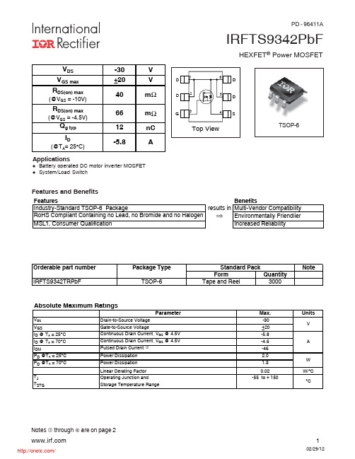
IRFTS9342PbFHEXFET ® Power MOSFETNotes through are on page 2Applicationsl Battery operated DC motor inverter MOSFET lSystem/Load SwitchFeatures and Benefitsresults in ⇒PD - 96411AIRFTS9342PbFNotes:Repetitive rating; pulse width limited by max. junction temperature. Pulse width ≤ 400μs; duty cycle ≤ 2%.When mounted on 1 inch square copper board.Static @ T = 25°C (unless otherwise specified)IRFTS9342PbFFig 4. Normalized On-Resistance vs. TemperatureFig 2. Typical Output CharacteristicsFig 1. Typical Output CharacteristicsFig 6. Typical Gate Charge vs.Gate-to-Source VoltageFig 5. Typical Capacitance vs.Drain-to-Source Voltage T J , Junction Temperature (°C)R D S (o n ) , D r a i n -t o -S o u r c e O n R e s i s t a n c e 110100-V DS , Drain-to-Source Voltage (V)10100100010000C , C a p a c i t a n c e (p F )0246810121416Q G Total Gate Charge (nC)0.02.04.06.08.010.012.014.0-V G S , G a t e -t o -S o u r c e V o l t a g e (V )DS -V DS , Drain-to-Source Voltage (V)0.1110100-I D , D r a i n -t o -S o u r c e C u r r e n t (A )IRFTS9342PbFFig 11. Maximum Effective Transient Thermal Impedance, Junction-to-CaseFig 8. Maximum Safe Operating AreaFig 9. Maximum Drain Current vs.Case TemperatureFig 7. Typical Source-Drain Diode Forward VoltageFig 10. Threshold Voltage vs. Temperature255075100125150T A , Ambient Temperature (°C)0123456-I D , D r a i n C u r r e n t (A)0.010.1110100V DS , Drain-to-Source Voltage (V)0.010.11101001000I D , D r a i n -t o -S o u r c e C u r r e n t (A)0.1110100-I S D , R e v e r s e D r a i n C u r r e n t (A )T J , Temperature ( °C )-V G S (t h ), G a t e t h r e s h o l d V o l t a g e (V )IRFTS9342PbFFig 12. On-Resistance vs. Gate VoltageFig 14. Maximum Avalanche Energy vs. Drain Current Fig 15. Typical Power vs. Time* Reverse Polarity of D.U.T for P-Channel* V GS = 5V for Logic Level Devices®2468101214161820-V GS, Gate -to -Source Voltage (V)255075100125150Starting T J , Junction Temperature (°C)020406080100120E A S , S i n g l e P u l s e A v a l a n c h e E n e r g y (m J )Time (sec)P o w e r (W )IRFTS9342PbFFig 17a. Gate Charge Test CircuitFig 17b. Gate Charge WaveformFig 18b. Unclamped Inductive WaveformsFig 18a. Unclamped Inductive Test CircuitFig 19b. Switching Time WaveformsFig 19a. Switching Time Test CircuitIdQgs1Qgs2Qgd QgodrV DDR DV DDI ASV DSV GSt t t tNote: For the most current drawing please refer to IR website at: /package/WW = (27-52) IF PRECEDED BY A LETTERYEA R Y Z52W WORK WEEK 26ZF = IRF5801(a s show n here) indica tes Lead-F ree.Note: A line above the w ork w eek G = IRF5803D = IRF5851E = IRF5852I = IRF 5805C = IRF5850N = IRF 5802K = IRF5810J = IRF5806H = IRF 5804S = Not a pplicable R = IRFTS 9342TRPBF T = IRLT S2242TRPBFIRFTS9342PbFTSOP-6 Tape and Reel Information† Qualification standards can be found at International Rectifier’s web site /product-info/reliability†† Higher qualification ratings may be available should the user have such requirements. Please contact your International Rectifier sales representative for further information: /whoto-call/salesrep/†††Applicable version of JEDEC standard at the time of product release.IR WORLD HEADQUARTERS: 101 N. Sepulveda Blvd., El Segundo, California 90245, USA Tel: (310) 252-7105TAC Fax: (310) 252-7903Visit us at for sales contact information . 02/2012Data and specifications subject to change without notice.8mmFEED DIRECTION4mmNOTES :1. OUTLINE CONFORMS TO EIA-481 & EIA-541.9.90 ( .390 )8.40 ( .331 )178.00( 7.008 ) MAX.NOTES:1. CONTROLLING DIMENSION : MILLIMETER.2. OUTLINE CONFORMS TO EIA-481 & EIA-541.Qualification information †分销商库存信息: IRIRFTS9342TRPBF。
IRFR220NTRPBF中文资料
Units
mJ A mJ
Thermal Resistance
Parameter
RθJC RθJA RθJA Junction-to-Case Junction-to-Ambient (PCB mount)* Junction-to-Ambient Parameter Continuous Source Current (Body Diode) Pulsed Source Current (Body Diode) Diode Forward Voltage Reverse Recovery Time Reverse RecoveryCharge Forward Turn-On Time
RDS(on) , Drain-to-Source On Resistance (Normalized)
I D , Drain-to-Source Current (A)
TJ = 25 ° C
10
3.0 2.5
TJ = 175 ° C
2.0 1.5
1
1.0
0.5 0.0 -60 -40 -20
0.1 4.0
Notes through are on page 10
1
11/29/00
元器件交易网
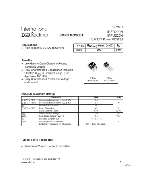
IRFR/U220N
Static @ TJ = 25°C (unless otherwise specified)
Parameter Drain-to-Source Breakdown Voltage ∆V(BR)DSS/∆TJ Breakdown Voltage Temp. Coefficient RDS(on) Static Drain-to-Source On-Resistance VGS(th) Gate Threshold Voltage V(BR)DSS IDSS IGSS Drain-to-Source Leakage Current Gate-to-Source Forward Leakage Gate-to-Source Reverse Leakage Min. Typ. Max. Units Conditions 200 ––– ––– V VGS = 0V, I D = 250µA ––– 0.23 ––– V/°C Reference to 25°C, ID = 1mA ––– ––– 600 mΩ VGS = 10V, I D = 2.9A 2.0 ––– 4.0 V VDS = VGS , ID = 250µA ––– ––– 25 VDS = 200V, VGS = 0V µA ––– ––– 250 VDS = 160V, VGS = 0V, T J = 150°C ––– ––– 100 VGS = 20V nA ––– ––– -100 VGS = -20V
AON5820;中文规格书,Datasheet资料

Crss
Reverse Transfer Capacitance
Rg
Gate resistance
VGS=0V, VDS=10V, f=1MHz VGS=0V, VDS=0V, f=1MHz
1000 1255 1510 pF
150 220 290 pF
100 168 235 pF
2.5
KΩ
SWITCHING PARAMETERS
Qrr
Body Diode Reverse Recovery Charge IF=10A, dI/dt=500A/µs
12
15
18
nC
A. The value of RθJA is measured with the device mounted on 1in2 FR-4 board with 2oz. Copper, in a still air environment with TA =25°C. The Power dissipation PDSM is based on R θJA and the maximum allowed junction temperature of 150°C. The value in any given application depends on the user's specific board design.
VDS=VGS, ID=250µA
0.3 0.65 1.0
V
ID(ON)
On state drain current
VGS=4.5V, VDS=5V
85
A
VGS=4.5V, ID=10A
5.5 7.4 9.5 mΩ
TJ=125°C 8
5810R使用手册
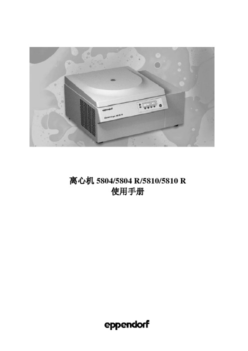
离心机 5804/5804 R/5810/5810 R使用手册图1 :5804 / 5810 (非冷冻离心机)显示界面和控制面板图2:5804 R/ 5810 R (冷冻离心机)显示界面和控制面板目录1.简介1.1.包装1.2.开箱1.3.仪器安装2.安全警告与应用限制3.操作3.1.控制键3.2.装载/装卸转子3.3.转子盖F-45—30—113.4.装上转子3.5.屏幕上显示预设时间/转速的常规离心3.6.持续运行3.7.瞬时离心3.8运行中时间变更3.9冷冻(仅对5804R/5810R)3.10预设半径3.11软启动/软停止离心3.12定速记时功能3.13预调程序3.14编辑状态3.15写保护3.16设定定值显示3.17自动转子识别3.18显示已运行时间3.19开关报警信号3.20退出服务程序3.21通过系列界面控制(可选)3.22断电情况下打开机器3.23断流器开关/保险4.保养与清洗4.1.主机4.2.转子4.3.气密型转子4.4.转子消毒4.5.玻璃破损4.6.冷冻离心机5.问题及解决方法6.技术参数1.简介5804/5810 是不带冷冻功能的台式离心机,5804R/5810R是带冷冻功能的台式离心机。
5804/5804R最大样品容量400ml,5810/5810R最大样品容量1600ml。
所有离心机适于医药以及科学研究等领域的实验室科学研究。
在离心机上和此操作手册里多处见到此标记。
注此标记的文字说明包含了安全注意。
第一次使用离心机前仔细阅读安全警告.在第一次启动5804/5810和5804R/5810R时,请仔细阅读使用手册。
1.1.运输包装1 带冷却风扇的5804/5810R离心机或者是冷冻型5804R/5810R(不包括转子)1 主电源线(欧式插座)1 使用手册1 转子起子1。
2 开箱从包装箱取离心机时,首先将仪器整个包装搬至承重桌面最近的位置,尔后需要两个人分别从仪器左右两侧底部接近橡皮脚附近的位置着手,将仪器放置水平桌面。
IRF8721TRPBF;IRF8721PBF;中文规格书,Datasheet资料
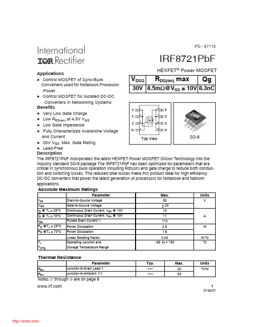
107/30/07IRF8721PbFHEXFET ®Power MOSFETBenefitsl Very Low Gate Charge l Low R DS(on) at 4.5V V GS l Low Gate Impedancel Fully Characterized Avalanche Voltage and Currentl 20V V GS Max. Gate Rating l Lead-Free Applicationsl Control MOSFET of Sync-BuckConverters used for Notebook Processor Powerl Control MOSFET for Isolated DC-DC Converters in Networking Systems SO-8PD - 97119DescriptionThe IRF8721PbF incorporates the latest HEXFET Power MOSFET Silicon Technology into the industry standard SO-8 package The IRF8721PbF has been optimized for parameters that are critical in synchronous buck operation including Rds(on) and gate charge to reduce both conduc-tion and switching losses. The reduced total losses make this product ideal for high efficiency DC-DC converters that power the latest generation of processors for Notebook and Netcom applications.IRF8721PbFStatic @ T = 25°C (unless otherwise specified)IRF8721PbF 3Fig 4. Normalized On-ResistanceVs. TemperatureFig 2. Typical Output CharacteristicsFig 1. Typical Output Characteristics Fig 3. Typical Transfer CharacteristicsV DS , Drain-to-Source Voltage (V)T J , Junction Temperature (°C)R D S (o n ) , D r a i n -t o -S o u r c e O n R e s i s t a n c e(N o r m a l i z e d )V GS , Gate-to-Source Voltage (V)V DS , Drain-to-Source Voltage (V)IRF8721PbFFig 8. Maximum Safe Operating AreaFig 6. Typical Gate Charge Vs.Gate-to-Source VoltageFig 5. Typical Capacitance Vs.Drain-to-Source VoltageFig 7. Typical Source-Drain DiodeForward Voltage110100V DS , Drain-to-Source Voltage (V)100100010000C , C a p a c i t a n c e (p F )0.11101001000I S D , R e v e r s e D r a i n C u r r e n t (A )0.1110100V DS , Drain-to-Source Voltage (V)0.11101001000I D , D r a i n -t o -S o u r c e C u r r e n t (A)510152025Q g , Total Gate Charge (nC)0481216V G S , G a t e -t o -S o u r c e V o l t a g e (V )IRF8721PbF 5Fig 11. Maximum Effective Transient Thermal Impedance, Junction-to-AmbientFig 9. Maximum Drain Current Vs.Case TemperatureFig 10. Threshold Voltage Vs. Temperature255075100125150T A , Ambient Temperature (°C)0481216I D , D r a i n C u r r e n t (A)T J , Temperature ( °C )V G S (t h ) G a t e t h r e s h o l d V o l t a g e (V )t 1, Rectangular Pulse Duration (sec)T h e r m a l R e s p o n s e ( Z t h J A )Fig 13. Maximum Avalanche Energyvs. Drain CurrentFig 12. On-Resistance vs. Gate VoltageFig 15b. Switching Time WaveformsFig 14b. Unclamped Inductive WaveformsFig 14a. Unclamped Inductive Test CircuitI ASFig 15a. Switching Time Test Circuit6810121416R D S (o n ), D r a i n -t o-S o u r c e O n R e s i s t a n c e (m Ω)V DDStarting T J , Junction Temperature (°C)V V d(on)rd(off)fV DDIRF8721PbF7DSCurrent Sampling ResistorsFig 16a. Gate Charge Test CircuitFig 16b. Gate Charge WaveformFig 17. Peak Diode Recovery dv/dt Test Circuit for N-ChannelHEXFET ® Power MOSFETs* V GS = 5V for Logic Level DevicesIdQgs1Qgs2Qgd QgodrIRF8721PbFSO-8 Package OutlineDimensions are shown in milimeters (inches)IRF8721PbF 9Notes:Repetitive rating; pulse width limited by max. junction temperature. Starting T J = 25°C, L = 1.09mH, R G = 25Ω, I AS = 11A. Pulse width ≤ 400μs; duty cycle ≤ 2%.When mounted on 1 inch square copper board. R θ is measured at T J of approximately 90°C.Data and specifications subject to change without notice.This product has been designed and qualified for the Consumer market.Qualification Standards can be found on IR’s Web site.IR WORLD HEADQUARTERS: 233 Kansas St., El Segundo, California 90245, USA Tel: (310) 252-7105TAC Fax: (310) 252-7903Visit us at for sales contact information .07/2007Note: For the most current drawing please refer to IR website at /package/330.00(12.992) MAX.14.40 ( .566 )12.40 ( .488 )NOTES :1. CONTROLLING DIMENSION : MILLIMETER.2. OUTLINE CONFORMS TO EIA-481 & EIA-541.FEED DIRECTIONTERMINAL NUMBER 112.3 ( .484 )11.7 ( .461 )8.1 ( .318 )7.9 ( .312 )NOTES:1. CONTROLLING DIMENSION : MILLIMETER.2. ALL DIMENSIONS ARE SHOWN IN MILLIMETERS(INCHES).3. OUTLINE CONFORMS TO EIA-481 & EIA-541.SO-8 Tape and ReelDimensions are shown in milimeters (inches)分销商库存信息:IRIRF8721TRPBF IRF8721PBF。
IRF5851TRPBF中文资料
IRF5851TRPBF中文资料Max.N-ChannelP-Channel V DSDrain-to-Source Voltage20-20I D @ T A = 25°CContinuousDrainCurrent,************.2ID@TA= 70°C Continuous Drain Current, V***********.7IDM Pulsed Drain Current 11-9.0P D @T A = 25°C Power Dissipation 0.96W P D @T A = 70°C Power Dissipation 0.62Linear Derating Factor 7.7mW/°C V GS Gate-to-Source Voltage± 12V T J, T STGJunction and Storage Temperature Range°C09/02/02IRF5851DescriptionParameterTyp.Max.UnitsR θJAMaximum Junction-to-Ambient–––130°C/WThermal Resistance 1These N and P channel MOSF ETs from International Rectifier utilize advanced processing techniques to achieve the extremely low on-resistance per silicon area. This benefit provides the designer with an extremely efficient device for use in battery and load management applications.This Dual TSOP-6 package is ideal for applications where printed circuit board space is at a premium and where maximum functionality is required.With two die per package, the IRF5851can provide the functionality of two SOT-23 packages in a smaller footprint. Its unique thermal design and R DS(on) reduction enables an increase in current-handling capability.ParameterUnitsAAbsolute Maximum Ratings-55 to + 150l Ultra Low On-Resistancel l Surface Mountl Available in Tape & Reel lLow Gate ChargePD-93998BIRF5851ParameterMin.Typ.Max. Units ConditionsN-Ch 20——V GS = 0V, I D = 250μA P-Ch -20——V GS = 0V, I D = -250μA N-Ch —0.016—Reference to 25°C, I D = 1mA P-Ch —-0.011—Reference to 25°C, I D = -1mA ——0.090V GS = 4.5V, I D = 2.7A ——0.120 V GS = 2.5V, I D = 2.2A ——0.135V GS = -4.5V, I D = -2.2A ——0.220V GS = -2.5V, I D = -1.7A N-Ch 0.60— 1.25V DS = V GS , I D = 250μA P-Ch -0.45—-1.2V DS = V GS , I D = -250μA N-Ch 5.2——V DS = 10V, I D = 2.7A P-Ch 3.5——V DS = -10V, I D = -2.2A N-Ch —— 1.0V DS = 16V, V GS = 0V P-Ch ——-1.0V DS = -16V, V GS = 0VN-Ch ——25V DS = 16V, V GS = 0V, T J = 70°C P-Ch ——-25V DS = -16V, V GS = 0V, T J = 70°C I GSS Gate-to-Source Forward Leakage N-P ––—±100V GS = ± 12VN-Ch — 4.0 6.0P-Ch — 3.6 5.4N-Ch —0.95—P-Ch —0.66—N-Ch —0.83—P-Ch — 5.7—N-Ch — 6.6—P-Ch —8.3—N-Ch — 1.2—P-Ch —14—N-Ch —15—P-Ch —31—N-Ch — 2.4—P-Ch —28—N-Ch —400—P-Ch —320—N-Ch —48—P-Ch —56—N-Ch —32—P-Ch—40—V (BR)DSSDrain-to-Source Breakdown VoltageV (BR)DSS /?T J Breakdown Voltage Temp. CoefficientR DS(ON)Static Drain-to-Source On-ResistanceV GS(th)Gate Threshold Voltage g fs F orward TransconductanceI DSS Drain-to-Source Leakage Current Q g T otal Gate Charge Q gs Gate-to-Source Charge Q gd Gate-to-Drain ("Miller") Charge t d(on)Turn-On Delay Time t r Rise Timet d(off)Turn-Off Delay Time t f Fall Time C iss Input Capacitance C oss Output CapacitanceC rssReverse Transfer CapacitanceElectrical Characteristics @ T J = 25°C (unless otherwise specified)VV/°CVSμAnCnspFN-ChannelI D = 2.7A, V DS = 10V, V GS = 4.5VP-ChannelI D = -2.2A, V DS = -10V, V GS = -4.5V N-ChannelV DD = 10V, I D = 1.0A, R G = 6.2?, V GS = 4.5VP-ChannelV DD = -10V, I D = -1.0A, R G = 6.0?, V GS = -4.5VN-ChannelV GS = 0V, V DS = 15V, ? = 1.0MHz P-ChannelV GS = 0V, V DS = -15V, ? = 1.0MHzN-ChP-ChRepetitive rating; pulse width limited bymax. junction temperature. ( See fig. 10 & 26 ) Surface mounted on FR-4 board, t ≤ 10sec.Pulse width ≤ 400μs; duty cycle ≤ 2%.Notes:ParameterMin.Typ.Max. Units Conditions N-Ch ——0.96P-Ch ——-0.96N-Ch ——11P-Ch ——-9.0N-Ch ——1.2T J = 25°C, I S = 0.96A, V GS = 0V P-Ch ——-1.2T J = 25°C, I S = -0.96A, V GS = 0V N-Ch —2538P-Ch —2335N-Ch — 6.59.8P-Ch—7.712Source-Drain Ratings and CharacteristicsI S Continuous Source Current (Body Diode)I SM Pulsed Source Current (Body Diode) V SD Diode Forward Voltage t rr Reverse Recovery Time Q rrReverse Recovery ChargeA V ns nC N-Channel T J = 25°C, I F = 0.96A, di/dt = 100A/μs P-ChannelT J = 25°C, I F = -0.96A, di/dt = -100A/μsIRF5851 3 N-Channel Vs. Temperature IRF5851Gate-to-Source Voltage Drain-to-Source Voltage Forward VoltageN-ChannelIRF5851 5N-ChannelCase TemperatureFig 10a. Switching Time Test Circuit V DSV d(on)rd(off)fFig 10b. Switching Time Waveforms V DDIRF5851N-ChannelFig 12. Typical On-Resistance Vs. Drain CurrentFig 11. Typical On-Resistance Vs. GateVoltageV GS, Gate -to -Source Voltage (V)R DS (o n ), D r a i n -t o -S o u r c e O n R e s i s t a n c e (?) Fig 13b. Gate Charge Test CircuitFig 13a.Basic Gate Charge Waveform V 4.5 VDSCurrent SamplingResistors24681012I D , Drain Current (A)0.000.100.200.30R D S (o n ) , D r a i n -t o -S o r c e O n R e s i s t a n c e (?) IRF5851 7Fig 14. Threshold Voltage Vs. Tempera-ture Fig 15. Typical Power Vs. TimeN-ChannelT J , Temperature ( °C )V G S (t h ) , V a r ia c e ( V )Time (sec)P o w e r (W )IRF5851 P-Channel Vs. Temperature IRF5851 9Gate-to-Source Voltage Drain-to-Source Voltage Forward VoltageP-ChannelIRF5851Junction TemperatureV DDV V t t t t Fig 25a. Switching Time Test Circuit Fig 25b. Switching Time WaveformsP-Channel11Fig 28. Typical On-Resistance Vs. DrainCurrentFig 27. Typical On-Resistance Vs. GateVoltageFig 29b. Gate Charge Test Circuit Fig 29a. Basic Gate Charge WaveformVDSCurrent Sampling ResistorsP-Channel-V GS, Gate -to -Source Voltage (V) RDS(on),Drain-to-SourceOnResitance()0246810-I D , Drain Current (A) 0.100.200.300.40RDS(on),Drain-t-SourceOnResistance()IRF5851P-ChannelT J , Temperature ( °C )-V G S (t h ) , V a r i a c e ( V ) Time (sec)P o w e r (W )IRF5851233 Kansas St., El Segundo, California 90245, USA Tel: (310) 252-7105TAC Fax: (310) 252-7903Visit us at for sales contact information. 09/02 。
IRS2101STRPBF中文资料
2
元器件交易网
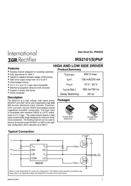
IRS2101(S)PbF
Dynamic Electrical Characteristics
VBIAS (VCC, VBS) = 15 V, CL = 1000 pF and TA = 25 °C unless otherwise specified.
50 1.0 0.625 125 200 150 150 300
Units
V
V/ns W
°C/W °C
Recommended Operating Conditions
The input/output logic timing diagram is shown in Fig. 1. For proper operation the device should be used within the recommended conditions. The VS offset rating is tested with all supplies biased at a 15 V differential.
Package power dissipation @ TA ≤ +25 °C
Thermal resistance, junction to ambient
Junction temperature Storage temperature Lead temperature (soldering, 10 seconds)
V
— 0.05 0.2
IO = 2 mA
— 0.02 0.1
—
—
50
VB = VS = 600 V
—
30 55
— 150 270 µA
VIN = 0 V or 5 V
ir2117strpbf规格书
ir2117strpbf规格书【实用版】目录1.产品概述2.主要特性3.规格参数4.应用领域5.环境要求6.安全信息7.结构说明8.工作原理9.测试方法10.维护与保养正文1.产品概述ir2117strpbf 是一种高性能、低成本的电子元器件,具有出色的稳定性和可靠性。
它广泛应用于各种电子设备和系统中,为设备提供稳定的电源和信号传输功能。
2.主要特性ir2117strpbf 具有以下主要特性:- 高稳定性:在恶劣的工作环境下,仍能保持稳定的工作性能。
- 低失真:信号传输过程中失真度低,保证了信号的完整性和准确性。
- 宽工作温度范围:能在 -40℃至 +125℃的温度范围内正常工作。
- 抗干扰能力强:能有效抵抗各种电磁干扰,保证设备的正常运行。
3.规格参数ir2117strpbf 的规格参数如下:- 电压范围:3.3V-5V- 电流范围:50mA-100mA- 工作温度范围:-40℃至 +125℃- 存储温度范围:-40℃至 +125℃- 抗静电能力:±15KV- 封装形式:SOP-84.应用领域ir2117strpbf 广泛应用于以下领域:- 电子消费品:如电视机、收音机、音响设备等。
- 通讯设备:如手机、电话机、传真机等。
- 计算机及周边设备:如电脑、路由器、打印机等。
- 工业控制设备:如工控机、可编程控制器等。
5.环境要求为了保证 ir2117strpbf 的正常工作和延长使用寿命,应满足以下环境要求:- 避免阳光直射和潮湿环境。
- 避免暴露在高温、低温、高湿度的环境中。
- 避免与腐蚀性物质接触。
- 避免强烈的机械振动和冲击。
6.安全信息在操作和使用 ir2117strpbf 时,请注意以下安全信息:- 请勿用湿手触摸或操作设备。
- 请勿在未断电的情况下拆卸设备。
- 请确保设备接地良好,以防止静电损伤。
- 如有异常现象,请立即停止使用并联系专业人员处理。
7.结构说明ir2117strpbf 的结构说明如下:- 引脚 1:电源正极(VCC)- 引脚 2:电源负极(GND)- 引脚 3:输出信号(OUT)- 引脚 4:控制信号(CTRL)- 引脚 5:公共地(GND)- 引脚 6:公共地(GND)- 引脚 7:公共地(GND)- 引脚 8:输出信号(OUT)8.工作原理ir2117strpbf 的工作原理如下:当控制信号(CTRL)为高电平时,输出信号(OUT)跟随输入信号;当控制信号为低电平时,输出信号呈高阻态。
- 1、下载文档前请自行甄别文档内容的完整性,平台不提供额外的编辑、内容补充、找答案等附加服务。
- 2、"仅部分预览"的文档,不可在线预览部分如存在完整性等问题,可反馈申请退款(可完整预览的文档不适用该条件!)。
- 3、如文档侵犯您的权益,请联系客服反馈,我们会尽快为您处理(人工客服工作时间:9:00-18:30)。
Source-Drain Ratings and Characteristics
IS
ISM
VSD trr Qrr
Parameter Continuous Source Current (Body Diode) Pulsed Source Current (Body Diode) Diode Forward Voltage Reverse Recovery Time Reverse Recovery Charge
10
ID = -2.9A VDS =-16V VDS =-10V
8
C, Capacitance (pF)
Ciss
600
6
400
4
200
Coss Crss
1 10 100
2
0
0
0
2
4
6
8
10
12
-VDS , Drain-to-Source Voltage (V)
QG , Total Gate Charge (nC)
2.0 2.5 3.0
0.0 -60 -40 -20
VGS = -4.5V
0 20 40 60 80 100 120 140 160
-VGS, Gate-to-Source Voltage (V)
TJ , Junction Temperature ( °C)
Fig 3. Typical Transfer Characteristics
Min. Typ. Max. Units ––– ––– ––– ––– 110 130 -1.0 -11 -1.2 170 200 V ns nC A
Conditions MOSFET symbol showing the G integral reverse p-n junction diode. TJ = 25°C, IS = -1.0A, VGS = 0V TJ = 25°C, IF = -1.0A di/dt = -100A/µs
TSOP-6
Absolute Maximum Ratings
Parameter
VDS ID @ TA = 25°C ID @ TA= 70°C IDM PD @TA = 25°C PD @TA = 70°C VGS TJ, TSTG Drain- Source Voltage Continuous Drain Current, VGS @ -4.5V Continuous Drain Current, VGS @ -4.5V Pulsed Drain Current Power Dissipation Power Dissipation Linear Derating Factor Gate-to-Source Voltage Junction and Storage Temperature Range
1
04/20/10
/
IRF5810PbF
Electrical Characteristics @ TJ = 25°C (unless otherwise specified)
V(BR)DSS
∆V(BR)DSS/∆TJ
Parameter Drain-to-Source Breakdown Voltage Breakdown Voltage Temp. Coefficient Static Drain-to-Source On-Resistance Gate Threshold Voltage Forward Transconductance Drain-to-Source Leakage Current Gate-to-Source Forward Leakage Gate-to-Source Reverse Leakage Total Gate Charge Gate-to-Source Charge Gate-to-Drain ("Miller") Charge Turn-On Delay Time Rise Time Turn-Off Delay Time Fall Time Input Capacitance Output Capacitance Reverse Transfer Capacitance
Fig 4. Normalized On-Resistance Vs. Temperature
3
/
IRF5810PbF
1000
-VGS , Gate-to-Source Voltage (V)
800
VGS = 0V, f = 1MHz Ciss = Cgs + Cgd , Cds SHORTED Crss = Cgd Coss = Cds + Cgd
PD - 95469B
IRF5810PbF
l l l l l l l
Ultra Low On-Resistance Dual P-Channel MOSFET Surface Mount Available in Tape & Reel Low Gate Charge Lead-Free Halogen-Free
0.1 0.4
0.1
-VSD ,Source-to-Drain Voltage (V)
100
-VDS , Drain-toSource Voltage (V)
Fig 7. Typical Source-Drain Diode Forward Voltage
Fig 8. Maximum Safe Operating Area
2.0
T J = 25°C
10.0
RDS(on) , Drain-to-Source On Resistance (Normalized)
ID = -2.9A
-I D, Drain-to-Source Current (Α )
1.5
T J = 150°C
1.0
1.0
0.5
0.1 1.0 1.5
VDS = -15V 20µs PULSE WIDTH
Typ. ––– 0.011 60 87 ––– ––– ––– ––– ––– ––– 6.4 1.2 1.7 8.2 14 62 53 650 110 86
Max. Units Conditions ––– V VGS = 0V, ID = -250µA ––– V/°C Reference to 25°C, ID = -1mA 90 VGS = -4.5V, ID = -2.9 mΩ 135 VGS = -2.5V, ID = -2.3A -1.2 V VDS = VGS, ID = -250µA ––– S VDS = -10V, ID = -2.9A -1.0 VDS = -16V, VGS = 0V µA -25 VDS = -16V, VGS = 0V, TJ = 70°C -100 VGS = -12V nA 100 VGS = 12V 9.6 ID = -2.9A 1.8 nC VDS = -10V 2.6 VGS = -4.5V ––– VDD = -10V ––– ID = -1.0A ns ––– RG = 6.0Ω ––– VGS = -4.5V ––– VGS = 0V ––– pF VDS = -16V ––– ƒ = 1kHz
D
S
Notes:
Repetitive rating; pulse width limited by
max. junction temperature.
Surface mounted on 1 in square Cu board
Pulse width ≤ 400µs; duty cycle ≤ 2%.
2
/
IRF5810PbF
100
VGS -10V -7.0V -4.5V -3.0V -2.5V -1.8V -1.5V BOTTOM -1.2V TOP
100
10
-I D , Drain-to-Source Current (A)
-I D , Drain-to-Source Current (A)
0.1 0.1
-VDS , Drain-to-Source Voltage (V)
-VDS , Drain-to-Source Voltage (V)
Fig 1. Typical Output Characteristics
Fig 2. Typical Output Characteristics
100.0
10
VGS -10V -7.0V -4.5V -3.0V -2.5V -1.8V -1.5V BOTTOM -1.2V TOP
1
0.1
-1.ห้องสมุดไป่ตู้V
1
-1.2V
20µs PULSE WIDTH TJ = 150 °C
1 10 100
0.01 0.1
20µs PULSE WIDTH TJ = 25 °C
1 10 100
OPERATION IN THIS AREA LIMITED BY R DS(on)
TJ = 150 ° C
10
100µsec 1 Tc = 25°C Tj = 150°C Single Pulse 0 1 10
1
1msec 10msec
TJ = 25 ° C V GS = 0 V
0.6 0.8 1.0 1.2 1.4
Max.
-20 -2.9 -2.3 -11 0.96 0.62 0.008 ± 12 -55 to + 150
Units
V A W mW/°C V °C
Thermal Resistance
Parameter
RθJA Maximum Junction-to-Ambient